Download - Technology of ZnSe detectors 2011
Basic process chart of the
manufacturing of ZnSe detectors for thickness gauges
Andrii Sofiienko – Chief Physicist, Ukratominstruments Corp.
Volodimir Degoda – Director of RPC “Arvina”, Dr. Sci. Phys.
2011

Table of contents I. The material for the detectors.
II. Production of crystals for the detectors.
III. Optical control of the crystals.
IV. Deposition of multilayer electrical contacts.
V. Control of the conductivity.
VI. Assembling the detector and the measuring unit.
VII. Control of the detector at different temperatures.
2
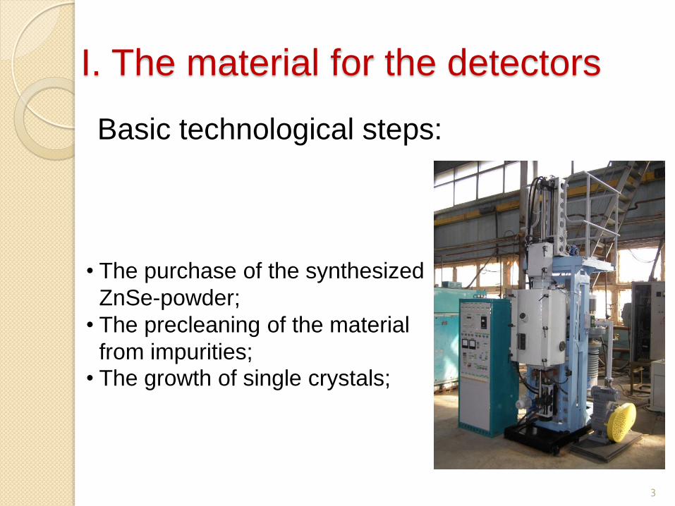
I. The material for the detectors
Basic technological steps:
3
• The purchase of the synthesized
ZnSe-powder;
• The precleaning of the material
from impurities; • The growth of single crystals;
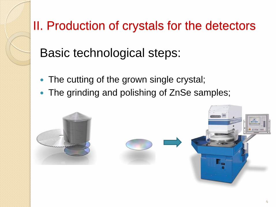
II. Production of crystals for the detectors
Basic technological steps:
The cutting of the grown single crystal;
The grinding and polishing of ZnSe samples;
4
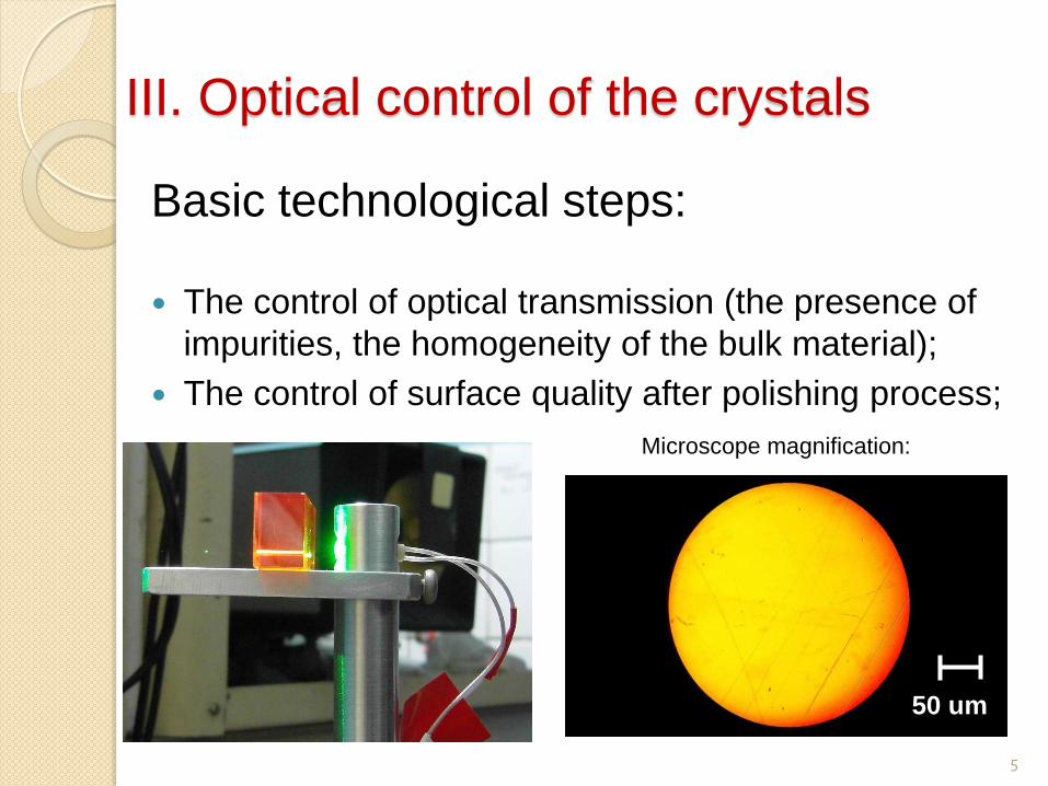
III. Optical control of the crystals
5
Basic technological steps:
The control of optical transmission (the presence of
impurities, the homogeneity of the bulk material);
The control of surface quality after polishing process;
50 um
Microscope magnification:

IV. Deposition of multilayer electrical contacts
6
Basic technological steps:
The usage of a "mask";
The resistive deposition of metal electrodes layer by layer (copper + silver);
1 – the vacuum cap, stainless steel; 2 -
valve, 3 - a pipeline for water heating or
cooling of the cap, 4 - needle leak to feed air
into the chamber, 5 - heating the substrate, 6
- substrate and the substrate, which can be
placed stencil; 7 - sealing gasket of the
vacuum rubber; 8 – the evaporator with a
substance placed in it and a heater
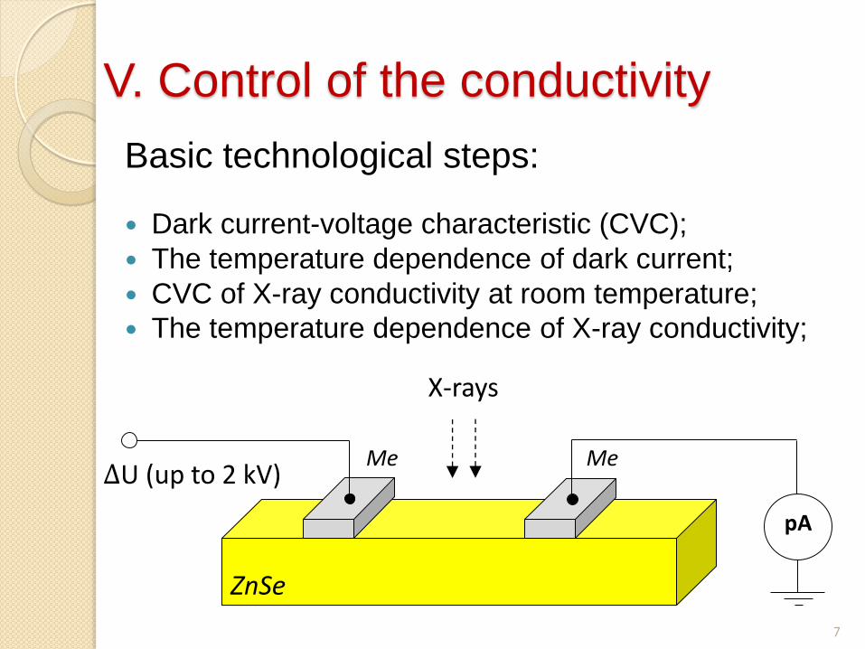
V. Control of the conductivity
7
Basic technological steps:
Dark current-voltage characteristic (CVC);
The temperature dependence of dark current;
CVC of X-ray conductivity at room temperature;
The temperature dependence of X-ray conductivity;
X-rays
∆U (up to 2 kV)
pA
ZnSe
Me Me
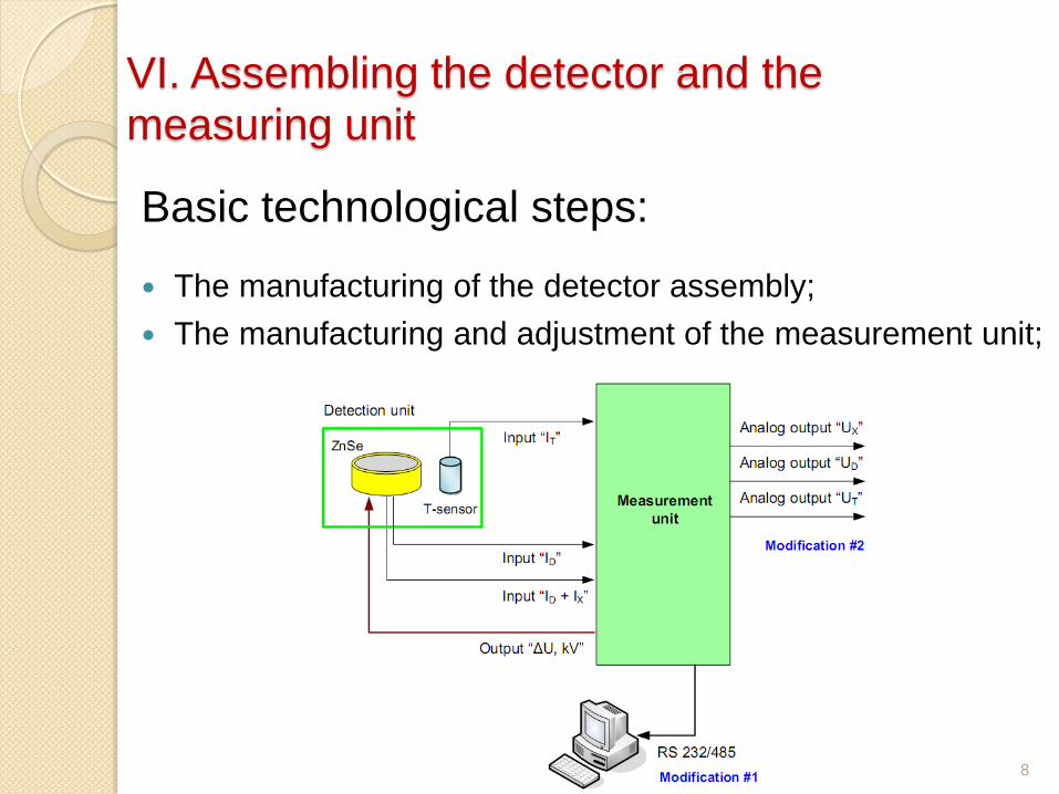
VI. Assembling the detector and the measuring unit
8
Basic technological steps:
The manufacturing of the detector assembly;
The manufacturing and adjustment of the measurement unit;
VII. Control of the detectors
9
Basic technological steps:
The control of dark conductivity of the detector at
different temperatures;
The test detector calibration function "intensity -
current - temperature";
The test of speed of detector (modulated pulsed radiation);
10 10
Research and Production Center “ARVINA”
Director: Degoda Volodymyr Yakovich
01033, Ukraine, Kiev, Saksaganskogo str., 31,
Tel: +38 066 2431530
E-mail: [email protected]
Contact information:


