Technical University Tallinn, ESTONIA
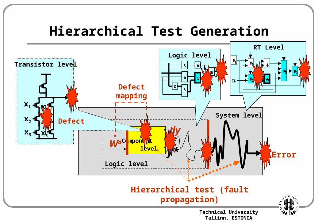
Component level
dy
Defect mapping
Hierarchical Test Generation
x1
x2
x3
x4
x5
System level
Wd
Logic levelError
Defect
Hierarchical test (fault propagation)
y*
&
&
&
1
&
&
&
R2M3
+M1
*M2
R1
IN
Logic level
Transistor level
RT Level
Research in ATI© Raimund Ubar
x1
x2
y
x3
x4 x5
x6 x7
0
11
0
x 1
x2
y
x 3
x4 x5
x6 x7
0
1
1
0
0
2
1
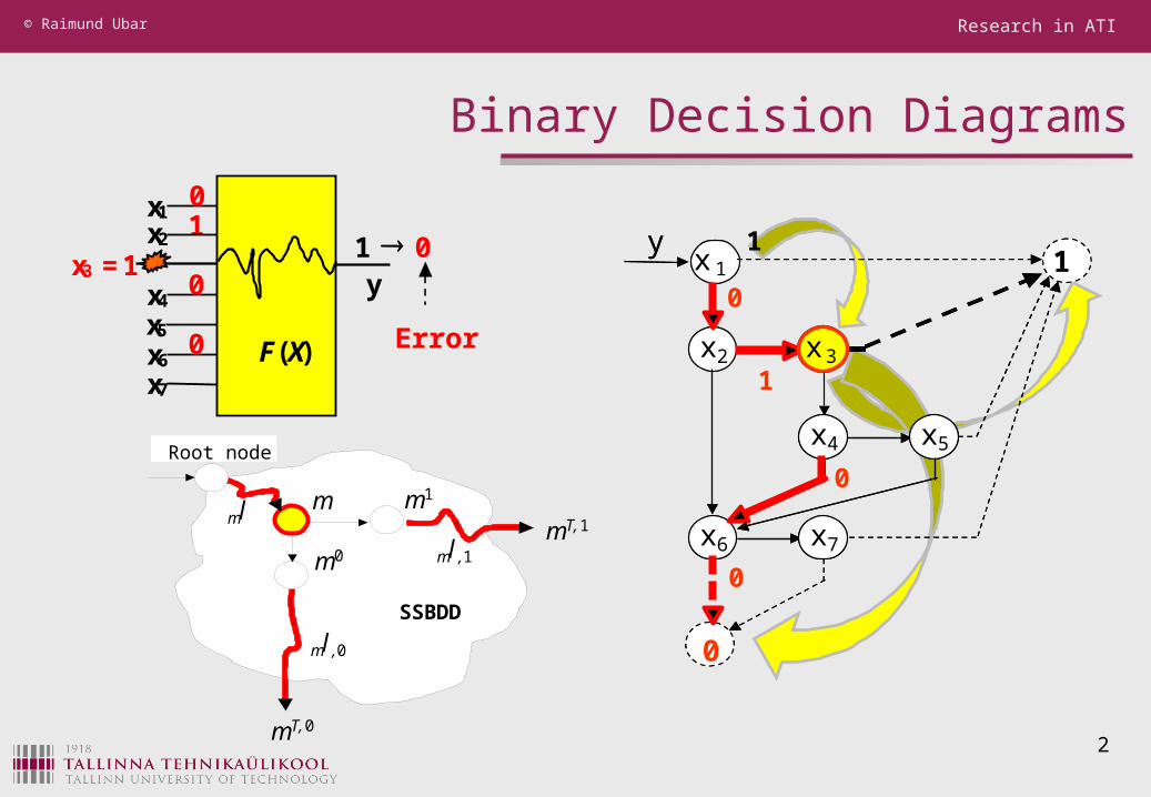
Error
1 0 x1 x2
x3 = 1 x4 x5 x6 x7
y
0
0 0 F (X)
SSBDD
mlm
lm ,1
m1
m0mT, 1
mT, 0
lm ,0
Root node
Binary Decision Diagrams

Research in ATI© Raimund Ubar
Generalization of BDDs
m
y1
0
lm
l1
l0
Gy
m
Y 1
0
2
h
FkFn
l0l1
l2lh
lklk+1
Fk+1
ln
lmGY
Binary DD 2 terminal nodes and 2 edges from each node
General case of DD n 2 terminal nodes and n 2 edges from each node
Novelty: Boolean methods can be generalized in a straightforward way to higher functional levels
3

Technical University Tallinn, ESTONIA
Faults and High-Level Decision Diagrams
RTL-statement:
R2M3
e+M1
a
*M2
b
R1
IN
c
d
y1 y2 y3 y4
y4
y3 y1 R1 + R2
IN + R2
R1* R2
IN* R2
y2
R2 0
1
2 0
1
0
1
0
1
0
R2
IN
R12
3
Terminal nodes
RTL-statement faults: data storage, data transfer, data manipulation faults
Nonterminal nodes
RTL-statement faults: label, timing condition, logical condition, register decoding, operation decoding,control faults
K: (If T,C) RD F(RS1,RS2,…RSm), N
Testing concepton the DD-model(uniform for all nodes): 1) Exhaustive testing2) Optimization
Technical University Tallinn, ESTONIA
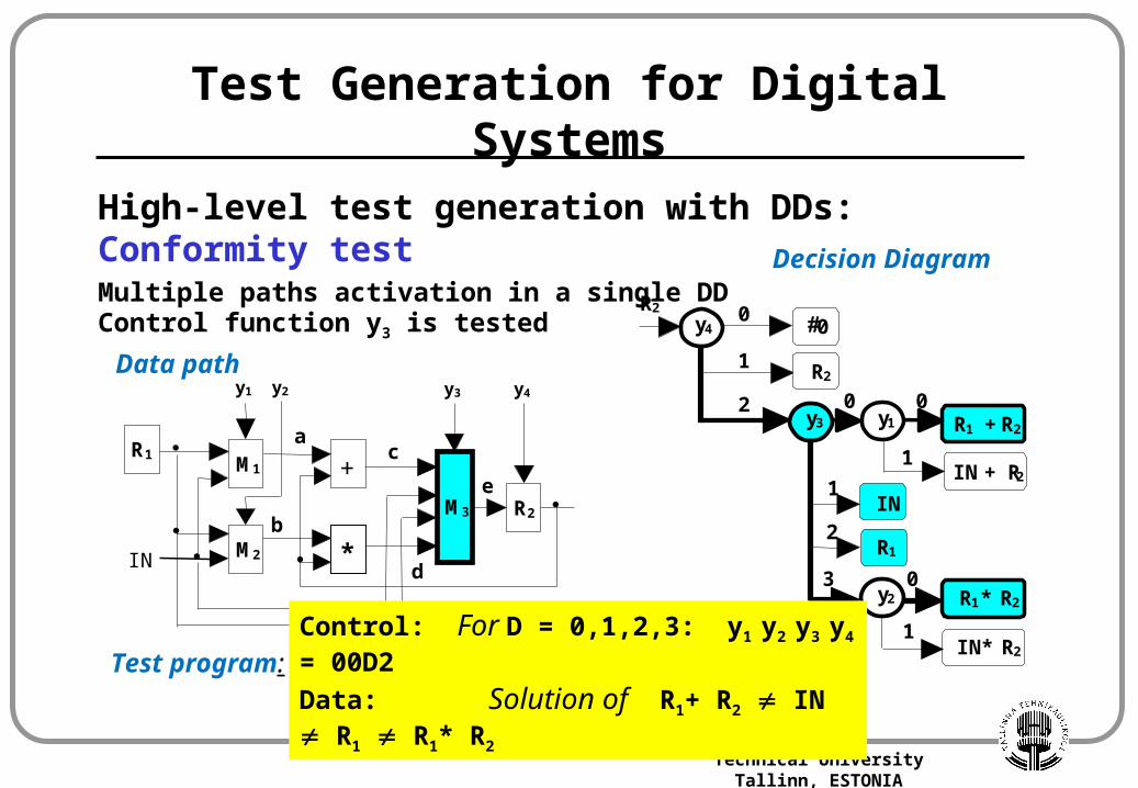
Test Generation for Digital Systems
R2M3
e+M1
a
*M2
b
R1
IN
c
d
y1 y2 y3 y4
y4
y3 y1 R1 + R2
IN + R2
R1 * R2
IN* R2
y2
R2 0
1
2 0
1
0
1
0
1
0
R2
IN
R12
3
Multiple paths activation in a single DDControl function y3 is tested
Data path
Decision Diagram
High-level test generation with DDs: Conformity test
Control: For D = 0,1,2,3: y1 y2 y3 y4 = 00D2
Data: Solution of R1+ R2 IN R1 R1* R2
Test program:

Technical University Tallinn, ESTONIA
Test Generation for Digital Systems
R2M3
e+M1
a
*M2
b
R1
IN
c
d
y1 y2 y3 y4
High-level test generation with DDs: Conformity test
Test template:Test program:
For D = 0,1,2,3BeginLoad R1 = IN1Load R2 = IN2Apply IN = IN3 y1 y2 y3 y4 = 00D2 Read R2 End
R2(D)
Control: For D = 0,1,2,3: y1 y2 y3 y4 = 00D2
Data: Solution of R1+ R2 IN R1 R1* R2

Technical University Tallinn, ESTONIA
Test Generation for Digital Systems
R2M3
e+M1
a
*M2
b
R1
IN
c
d
y1 y2 y3 y4
y4
y3 y1 R1 + R2
IN + R2
R1 * R2
IN* R2
y2
R2 0
1
2 0
1
0
1
0
1
0
R2
IN
R12
3
Single path activation in a single DDData function R1* R2 is tested
Data path
Decision Diagram
High-level test generation with DDs: Scanning test
Control: y1 y2 y3 y4 = 0032
Data: For all specified pairs of (R1, R2)
Test program:

Technical University Tallinn, ESTONIA
Test Generation for Digital Systems
R2M3
e+M1
a
*M2
b
R1
IN
c
d
y1 y2 y3 y4
High-level test generation with DDs: Scanning test
Control: y1 y2 y3 y4 = 0032
Data: For all specified pairs of (R1, R2)
Test template:Test program:
For j=1,nBeginLoad R1 = IN(j1)Load R2 = IN(j2)y1 y2 y3 y4 = 0032: Read R2 End
IN(j1) IN(j2) R2(j)
Test data Test results

Technical University Tallinn, ESTONIA
Scan-Path for Making Systems Transparent
y4
y3 y1 R1 + R2
IN + R2
R1 * R2
IN* R2
y2
R2 0
1
2 0
1
0
1
0
1
0
R2
IN
R12
3
Hierarhical test generation with Scan-Path:
Bus
Scan-Out
M3
e+M1
a
*M2
b
R1
IN
c
d
y1 y2 y3 y4
Control Part
R2
Scan-In
Data Part

Technical University Tallinn, ESTONIA
Testing with Minimal DFT for Scan-Path
M3
e+M1
a
*M2
b
R1
IN
c
d
y1 y2 y3 y4
y4
y3 y1 R1 + R2
IN + R2
R1 * R2
IN* R2
y2
R2 0
1
2 0
1
0
1
0
1
0
R2
IN
R12
3
Hierarhical test generation with Scan-Path:
Control Part
R2Bus
Scan-In
Scan-Out
Data Part

Technical University Tallinn, ESTONIA
Test Generation for Microprocessors
I1: MVI A,D A IN
I2: MOV R,A R A
I3: MOV M,R OUT R
I4: MOV M,A OUT IA
I5: MOV R,M R IN
I6: MOV A,M A IN
I7: ADD R A A + R
I8: ORA R A A R
I9: ANA R A A R
I10: CMA A,D A A
Test program generation for a microprocessor (example):
Instruction set:
I R3
A
OUT4
I A2
R
IN5
R
1,3,4,6-10
I IN1,6
A
A2,3,4,5
A + R7
A R8
A R9
A10
DD-model of themicroprocessor:
Technical University Tallinn, ESTONIA
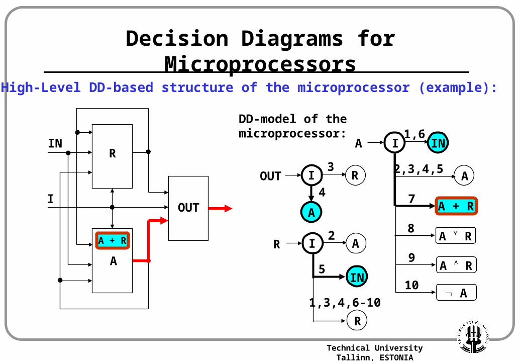
Decision Diagrams for Microprocessors
High-Level DD-based structure of the microprocessor (example):
DD-model of themicroprocessor:
OUT
R
A
IN
I
I R3
A
OUT4
I A2
R
IN5
R
1,3,4,6-10
I IN1,6
A
A2,3,4,5
A + R7
A R8
A R9
A10
A + R

Technical University Tallinn, ESTONIA
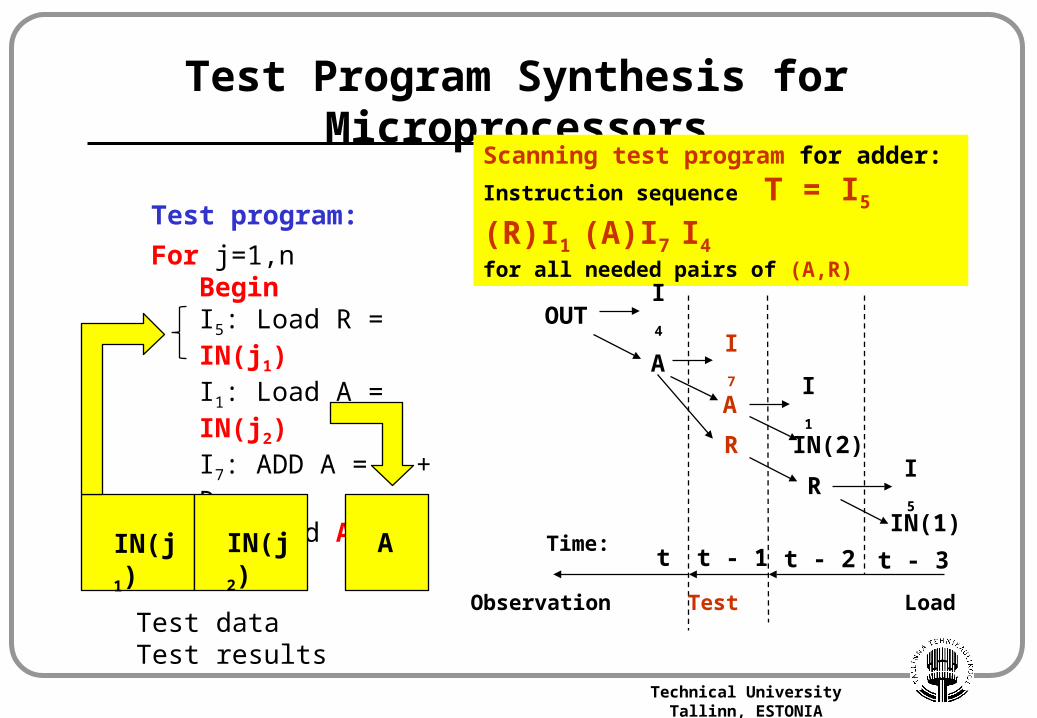
Test Program Synthesis for Microprocessors
DD-model of themicroprocessor:
Scanning test program for adder:
Instruction sequence T = I5 (R)I1 (A)I7 I4for all needed pairs of (A,R)
OUT I4
A I7
A
R
I1
IN(2)
IN(1)
R I5
Time:t t - 1 t - 2 t - 3
Observation Test Load
I R3
A
OUT4
I A2
R
IN5
R
1,3,4,6-10
I IN1,6
A
A2,3,4,5
A + R7
A R8
A R9
A10
Technical University Tallinn, ESTONIA
Test Program Synthesis for Microprocessors
Scanning test program for adder:
Instruction sequence T = I5 (R)I1 (A)I7 I4for all needed pairs of (A,R)
OUT I4
A I7
A
R
I1
IN(2)
IN(1)
R I5
Time:t t - 1 t - 2 t - 3
Observation Test Load
Test program:
For j=1,nBeginI5: Load R = IN(j1)I1: Load A = IN(j2)I7: ADD A = A + RI4: Read A End
IN(j1) IN(j2) A
Test data Test results

Technical University Tallinn, ESTONIA
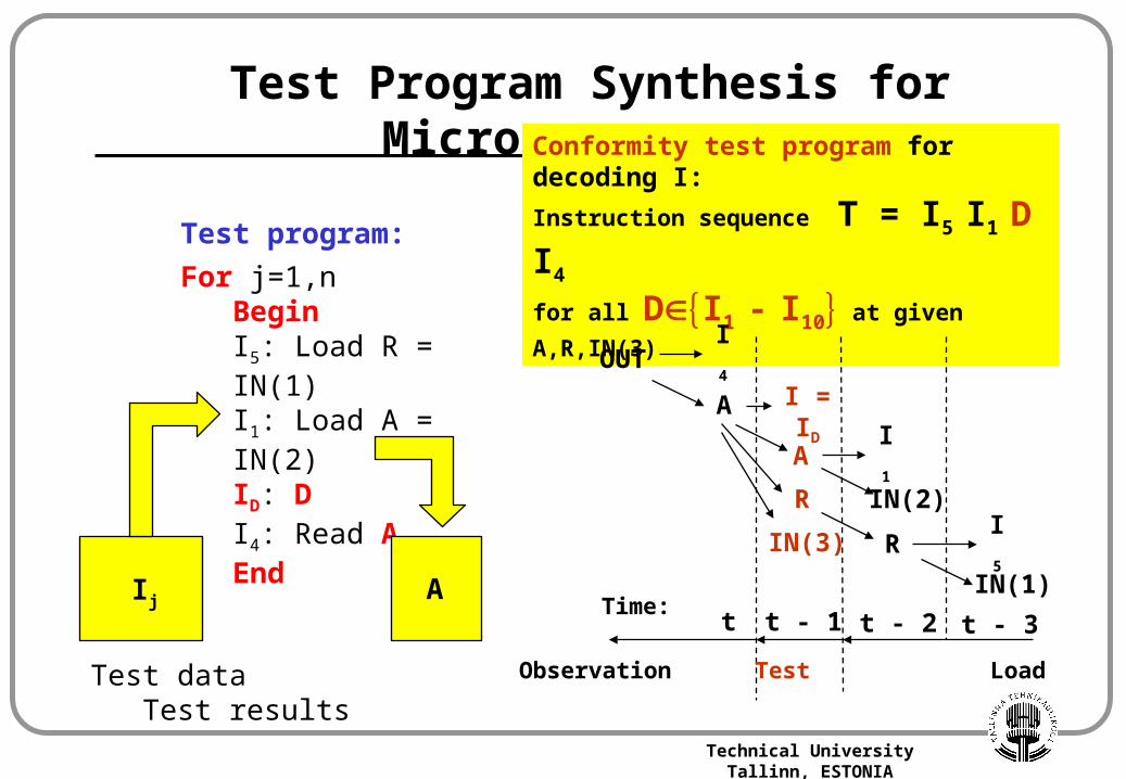
Test Program Synthesis for Microprocessors
DD-model of themicroprocessor:
Conformity test program for decoding I:
Instruction sequence T = I5 I1 D I4
for all DI1 - I10 at given A,R,IN(3)
OUT I4
A I = ID
A
R
I1
IN(2)
IN(1)
R I5
Time:t t - 1 t - 2 t - 3
Observation Test Load
I R3
A
OUT4
I A2
R
IN5
R
1,3,4,6-10
A I IN1,6
A2,3,4,5
A + R7
A R8
A R9
A10
IN(3)
Technical University Tallinn, ESTONIA
Test Program Synthesis for Microprocessors
Conformity test program for decoding I:
Instruction sequence T = I5 I1 D I4
for all DI1 - I10 at given A,R,IN(3)
OUT I4
A I = ID
A
R
I1
IN(2)
IN(1)
R I5
Time:t t - 1 t - 2 t - 3
Observation Test Load
IN(3)
Test program:
For j=1,nBeginI5: Load R = IN(1)I1: Load A = IN(2)ID: DI4: Read A End
Ij A
Test data Test results

Technical University Tallinn, ESTONIA
Test Data for Microrocessors
Conformity test program for I in A:
Instruction sequence T = I5 I1 D I4
for all DI1 - I10 at given A,R,IN
IN 110 A 101
Data
R 110 I1, I6 IN 110
I2, I3 I4, I5 A 101 I7 A + R 1011 I8 A R 111 I9 A R 00
Functions
I10 A 010
Data IN,A,R are generated so that the values of all functions were different
Response: RRR
Test: DTest data generation:
IN A ( A+R) (AR) ( AR) A
Find IN, A, R by solving the inequality:
A I IN1,6
A2,3,4,5
A + R7
A R8
A R9
A10

Technical University Tallinn, ESTONIA
Test Data for Microrocessors
Conformity test program for decoder:
Instruction sequence T = I5 I1 D I4
for all DI1 - I10 at given A,R,IN
Data generation:
IN 110 A 101
Data
R 110 I1, I6 IN 110
I2, I3 I4, I5 A 101 I7 A + R 1011 I8 A R 111 I9 A R 00
Functions
I10 A 010
Data IN,A,R are generated so that the values of all functions were different
Final test program:
Step I Mode IN A R
1 I5 Load R 110
2 I1 Load A 101 110
3 ID Test 110 101 110
4 I4 Observe RRR
Response: RRR
Test: D
IN A ( A+R) (AR) ( AR) A
Find IN, A, R by solving the inequality:
Research in ATI© Raimund Ubar
19
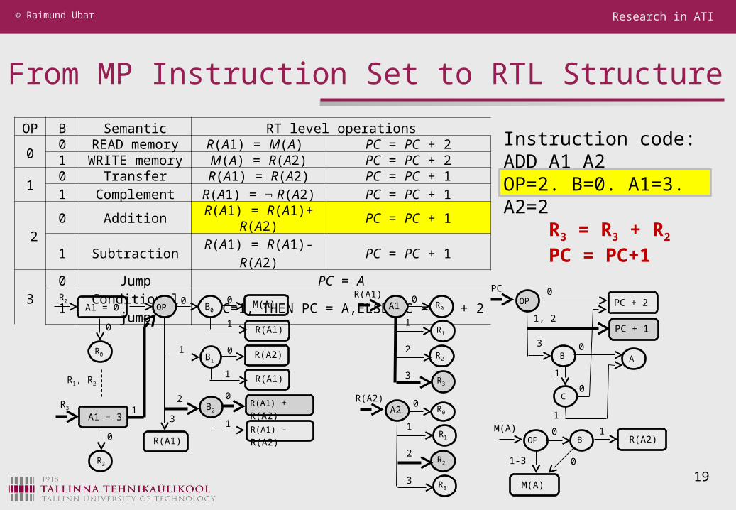
OP B Semantic RT level operations
00 READ memory R(A1) = M(A) PC = PC + 21 WRITE memory M(A) = R(A2) PC = PC + 2
10 Transfer R(A1) = R(A2) PC = PC + 11 Complement R(A1) = R(A2) PC = PC + 1
20 Addition R(A1) = R(A1)+ R(A2) PC = PC + 11 Subtraction R(A1) = R(A1)- R(A2) PC = PC + 1
30 Jump PC = A1 Conditional jump IF C=1, THEN PC = A,ELSE PC = PC + 2
From MP Instruction Set to RTL Structure
OP B0M(A) 1
R(A2)
M(A)
01-3
OP0PC
1, 2
B
3
A0
PC + 2
PC + 1
C
1
0
1
A1 R00R(A1)
R1
1
R2
2
R33
A2 R00R(A2)
R1
1
R2
2
R33
A1 = 0R0
R0
0
1
A1 = 3R3
R3
0
1
R1, R2
OP B0
0 M(A)
1
0
B1
1 R(A2)
1
0
B2
2
1
0
R(A1) - R(A2) 3
R(A1)
R(A1)
R(A1) + R(A2)
R(A1)
Instruction code:ADD A1 A2OP=2. B=0. A1=3. A2=2 R3 = R3 + R2
PC = PC+1

Research in ATI© Raimund Ubar
20
HLDDs for MP InstrSet
A1 = 0R0
R0
0
OP B0
1 0 M(A)
1
0
B1
1 R(A2)
1
0
B2
2
1
0
R(A1) - R(A2) 3A1 = 3
R3
R3
0
1
R1, R2
R(A1)
R(A1)
R(A1) + R(A2)
R(A1)
Registers and ALUA1 R0
0R(A1)
R1
1
R2
2
R33
A2 R00R(A2)
R1
1
R2
2
R33
Register Decoding OP0PC
1, 2
B
3
A0
PC + 2
PC + 1
C
1
0
1
Program Counter
OP B0M(A) 1
R(A2)
M(A)
01-3
Memory Access
Instruction code:ADD A1 A2OP=2. B=0. A1=3. A2=2 R3 = R3 + R2
PC = PC+1

Research in ATI© Raimund Ubar
21
Scanning Test Algorithm
Test Algorithm for the terminal node m in HLDD Gz
FOR t = 1,2, …, pInitialize the data registers R(m) with R(m,t) Execute the working mode under testREAD the result .
END.
The number p depends on how many operands is needed for testing the function of the terminal node
A1 = 0R0
R0
0
1
A1 = 3R3
R3
0
1
R1, R2
OP B0
0 M(A)
1
0
B1
1 R(A2)
1
0
B2
2
1
0
R(A1) - R(A2) 3
R(A1)
R(A1)
R(A1) + R(A2)
R(A1)
Terminal node mData registersR(A1), R(A2)to be initialized
Data register R3 to be read

Research in ATI© Raimund Ubar
22
Example: Scanning Test Program
OP B0M(A) 1
R(A2)
M(A)
01-3
OP0PC
1, 2
B
3
A0
PC + 2
PC + 1
C
1
0
1
A1 R00R(A1)
R1
1
R2
2
R33
A2 R00R(A2)
R1
1
R2
2
R33
A1 = 0R0
R0
0
1
A1 = 3R3
R3
0
1
R1, R2
OP B0
0 M(A)
1
0
B1
1 R(A2)
1
0
B2
2
1
0
R(A1) - R(A2) 3
R(A1)
R(A1)
R(A1) + R(A2)
R(A1)
FOR t =0,1,2, … , nLDA 2, A(0+t) (Initialize R2 = R2(t))LDA 3, A(10+t) (Initialize R3 = R3(t))ADD 3, 2 (Execute the instruction OP.B.A1.A2 = 2.0.3.2) STA A(20+t),2 (Write the content of R3 into M(20+t))
END FOR
Research in ATI© Raimund Ubar
23
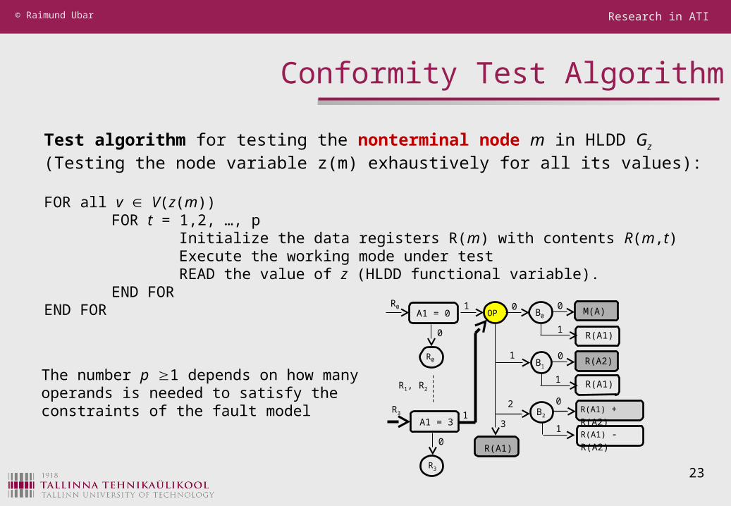
Conformity Test Algorithm
Test algorithm for testing the nonterminal node m in HLDD Gz
(Testing the node variable z(m) exhaustively for all its values):
FOR all v V(z(m)) FOR t = 1,2, …, p Initialize the data registers R(m) with contents R(m,t) Execute the working mode under test READ the value of z (HLDD functional variable). END FOREND FOR
The number p 1 depends on how many operands is needed to satisfy the constraints of the fault model
A1 = 0R0
R0
0
1
A1 = 3R3
R3
0
1
R1, R2
OP B0
0 M(A)
1
0
B1
1R(A2)
1
0
B2
2
1
0
R(A1) - R(A2) 3
R(A1)
R(A1)
R(A1) + R(A2)
R(A1)
Research in ATI© Raimund Ubar
24
Example: Conformity Test Program
OP B0M(A) 1
R(A2)
M(A)
01-3
OP0PC
1, 2
B
3
A0
PC + 2
PC + 1
C
1
0
1
A1 R00R(A1)
R1
1
R2
2
R33
A2 R00R(A2)
R1
1
R2
2
R33
A1 = 0R0
R0
0
1
A1 = 3R3
R3
0
1
R1, R2
OP B0
0 M(A)
1
0
B1
1 R(A2)
1
0
B2
2
1
0
R(A1) - R(A2) 3
R(A1)
R(A1)
R(A1) + R(A2)
R(A1)
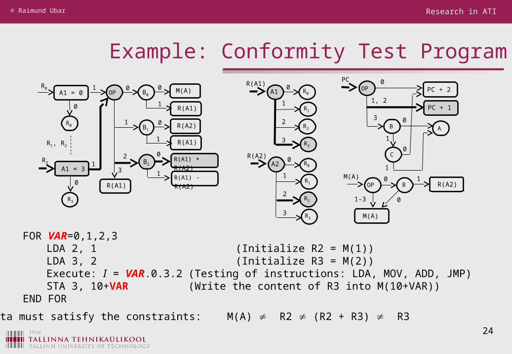
FOR VAR=0,1,2,3LDA 2, 1 (Initialize R2 = M(1))LDA 3, 2 (Initialize R3 = M(2))Execute: I = VAR.0.3.2 (Testing of instructions: LDA, MOV, ADD, JMP)STA 3, 10+VAR (Write the content of R3 into M(10+VAR))
END FOR
Data must satisfy the constraints: M(A) R2 (R2 + R3) R3

Research in ATI© Raimund Ubar
25
Fault Activating in Microprocessors
For testing a node, three actions are needed:- Local fault activating at a node by satisfying the constraints- Topologigal propagation of the fault through the HLDD- System level propagation of a fault through the system of HLDDs
i,j V(z(m)) [z(mi) (z(mj)]
Constraints for testing the node m
New fault model:m
Rm1
mv*v*
m0
mkk
mn
n
V*
1

Research in ATI© Raimund Ubar
State of Art: Microprocessor Fault Model
Source decoding (MUX):F1: no source is selectedF2: wrong source is selected;F3: more than one source is selected
and the multiplexer output is either a wired-AND or a wired-OR function of the sources, depending on the technology.
Destination decoding (DMUX)F4: no destination is selectedF5: instead of, or in addition to
the selected correct destination, one or more other destinations selected
Instruction exec. faultsF6: one or more microorders not
activated F7: microorders are erroneously
activatedF8: a different set of microinstructions is activated instead of, or in addition to
Data storage/bus/ALU faults: F9: one or more cells SAF0 /1;F10: one or more cells fail 01/10F11: two or more cells coupled; F12: one or more lines SAF0 /1;F13: one or more lines wired-OR/ANDF14: data manipulation faults
Thatte’1980

Research in ATI© Raimund Ubar
27
Fault Modeling in Microprocessors

Research in ATI© Raimund Ubar
28
Fault Modeling in Microprocessors
Research in ATI© Raimund Ubar
Hard-to-Test Faults in Microprocessors
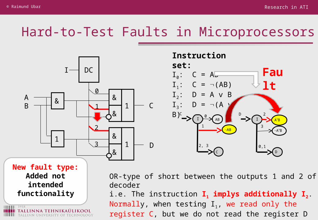
Instruction set:I0: C = ABI1: C = (AB)I2: D = A v BI3: D = (A v B)
OR-type of short between the outputs 1 and 2 of decoderi.e. The instruction I1 implys additionally I2.Normally, when testing I1, we read only the register C, but we do not read the register D
I AB0C
AB1
C
2, 3
I AB
2D
AB3
D
0,1
New fault type:Added not intended
functionality
DC
&
&1
&
1 &
&1
I
AB C
D
0
1
2
3
Fault

Research in ATI© Raimund Ubar
30
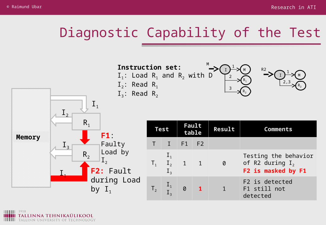
Instruction set:I1: Load R1 and R2 with DI2: Read R1
I3: Read R2
Fault Masking in Microprocessors

Research in ATI© Raimund Ubar
31
Instruction Based Test with Fault Masking
Memory
R1
R2
I1
F2: Fault during Load by I1
I2
F1: Faulty Load by I2I3
Instruction set:I1: Load R1 and R2 with DI2: Read R1
I3: Read R2
I1
Testing the instruction I1:I1: R1= D, R2=D* (D* is a faulty value)I2: Read R1 (correct reading), but R2 = D (the faulty value D* is overwritten with the correct value of D) I3: Read R2 (correct reading, the fault F2 was escaped).

Research in ATI© Raimund Ubar
Avoidance of Fault Masking
Memory
R1
R2
I1
F2: Fault during Load by I1
I2
F1: Faulty Load by I2I3
Instruction set:I1: Load R1 and R2 with DI2: Read R1
I3: Read R2
I1
In the proposed approach, instead of testing the instruction, we test the the functional variables R1 and R2 separately:Testing R1:I1: R1=D, R2=D* (D* is the faulty value)I2: Read R1 = D (correct reading) Testing R2:I1: R1=D, R2=D* (D* is the faulty value)I3: Read R2 = D* (the fault is detected)
Research in ATI© Raimund Ubar
Diagnostic Capability of the Test
Memory
R1
R2
I1
F2: Fault during Load by I1
I2
F1: Faulty Load by I2I3
Instruction set:I1: Load R1 and R2 with DI2: Read R1
I3: Read R2
I1
TestFault table
Result Comments
T I F1 F2
T1
I1I2I3
1 1 0Testing the behavior of R2 during I2F2 is masked by F1
T2
I1I3
0 1 1F2 is detectedF1 still not detected
I M1R2
R2
2,3
I M1M
R1
2
R2
3
Research in ATI© Raimund Ubar
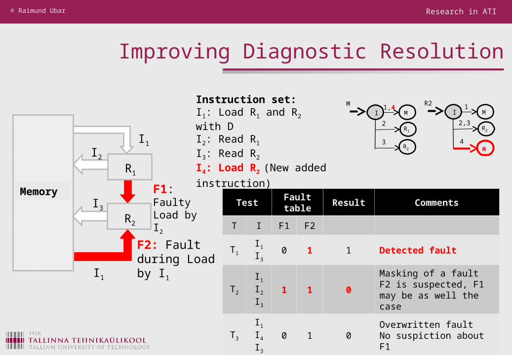
Improving Diagnostic Resolution
Memory
R1
R2
I1
F2: Fault during Load by I1
I2
F1: Faulty Load by I2I3
Instruction set:I1: Load R1 and R2 with DI2: Read R1
I3: Read R2
I4: Load R2 (New added
instruction)
I1
TestFault table
Result Comments
T I F1 F2
T1
I1I3
0 1 1 Detected fault
T2
I1I2I3
1 1 0Masking of a fault F2 is suspected, F1 may be as well the case
T3
I1I4I3
0 1 0Overwritten faultNo suspiction about F1
I M1R2
R2
2,3
M4
I M1,4M
R1
2
R2
3
Research in ATI© Raimund Ubar
35
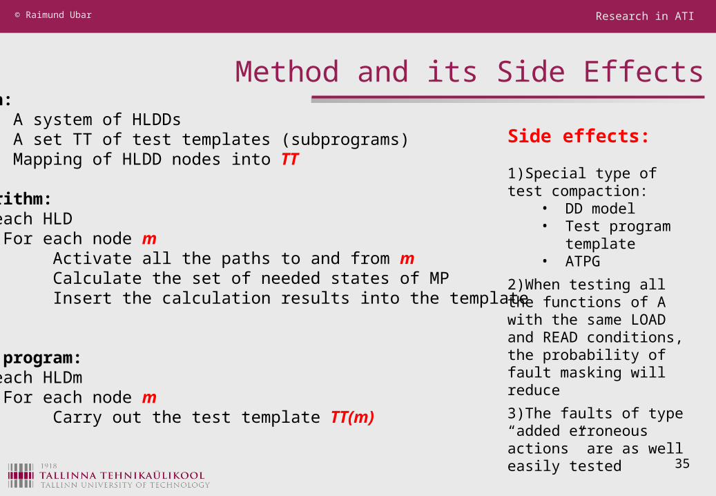
Method and its Side Effects
Side effects:
1)Special type of test compaction:
• DD model• Test program
template• ATPG
2)When testing all the functions of A with the same LOAD and READ conditions, the probability of fault masking will reduce
3)The faults of type “added erroneous actions” are as well easily tested
Given: A system of HLDDs A set TT of test templates (subprograms) Mapping of HLDD nodes into TT
Algorithm:For each HLD For each node m Activate all the paths to and from m Calculate the set of needed states of MP Insert the calculation results into the templateEND
Test program:For each HLDm For each node m Carry out the test template TT(m)END
Research in ATI© Raimund Ubar
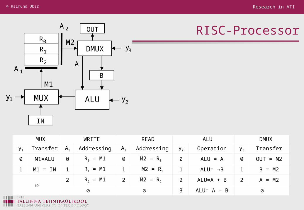
MUX WRITE READ ALU DMUX
y1 Transfer A1 Addressing A2 Addressing y2 Operation y3 Transfer
0 M1=ALU 0 R0 = M1 0 M2 = R0 0 ALU = A 0 OUT = M2
1 M1 = IN 1 R1 = M1 1 M2 = R1 1 ALU= B 1 B = M2
2 R2 = M1 2 M2 = R2 2 ALU=A + B 2 A = M2
3 ALU= A - B
RISC-ProcessorDMUX1 y3DMUX
ALU
A 1
R0
R1
R2
R0
R1
R2
RB
MUXy1 MUXy
ROUTA 2
y2
M1
RIN
M2
A

0 M1R0 A1
R0
R1 A1
R0
R2 A1
R0
1
2
M1y1
0
IN
0y2 A
B
A+B
1
2
A-B3
10
OUT y3A2 R0
B y3
B
R1
R1
1
2
0
1
A y3
2
DMUX1 y3DMUX
ALU
A 1
R0
R1
R2
R0
R1
R2
RB
MUXy1 MUXy
ROUTA 2
y2
M1
RIN
M2
A
MUX WRITE READ ALU DMUXy1 Transfer A1 Addressing A2 Addressing y2 Operation y3 Transfer
0 M1=ALU 0 R0 = M1 0 M2 = R0 0 ALU = A 0 OUT = M2
1 M1 = IN 1 R1 = M1 1 M2 = R1 1 ALU= B 1 B = M2
2 R2 = M1 2 M2 = R2 2 ALU=A + B 2 A = M2
3 ALU= A - B
RISC Processor and its HLDD model
Register block
Output behaviour ALU

0 M1R0 A1
R0
R1 A1
R0
R2 A1
R0
1
2
M1y1
0
IN
0y2 A
B
A+B
1
2
A-B3
10
OUT y3A2 R0
B y3
B
R1
R1
1
2
0
1
A y3
2
0OUT y3 A2 R0
y3B R1
R2
1
2
0
1
0M1A1
A1
A1
1
2
y1
0
IN
0y2 A
B
A+B
1
2
A-B3
1
A y3
2
RISC Processor and its HLDD model
Network level model
System level model
0OUT y3 A2 R0
y3B R1
R2
1
2
0
1
0M1A1
A1
A1
1
2
y1
0
IN
0y2 A
B
A+B
1
2
A-B3
1
A y3
2
0OUT y3 A2 R0
y3B R1
R2
1
2
0
1
0M1A1
A1
A1
1
2
y10
IN
0y2 A
B
A+B
1
2
A-B3
1
A y3
2
T y1 y2 y3 A1 A2 IN R0 R1 R2 B A OUT
1 1 0 D1 D1
T y1 y2 y3 A1 A2 IN R0 R1 R2 B A OUT
2 0 0 2 1 0 D1 D1 D1
Test Program Generation: Test 1Test step 1: Load R0
Test step 2: Testing ALU (M1 = A, Transfer A to R1)
0OUT y3 A2 R0
y3B R1
R2
1
2
0
1
0M1A1
A1
A1
1
2
y1
0
IN
0y2 A
B
A+B
1
2
A-B3
1
A y3
2
0OUT y3 A2 R0
y3B R1
R2
1
2
0
1
0M1A1
A1
A1
1
2
y1
0
IN
0y2 A
B
A+B
1
2
A-B3
1
A y3
2
T y1 y2 y3 A1 A2 IN R0 R1 R2 B A OUT
3 1 0 2 1 D2 D1 D1 D2 D1
T y1 y2 y3 A1 A2 IN R0 R1 R2 B A OUT
4 1 1 0 2 D3 D3 D1 D2 D2
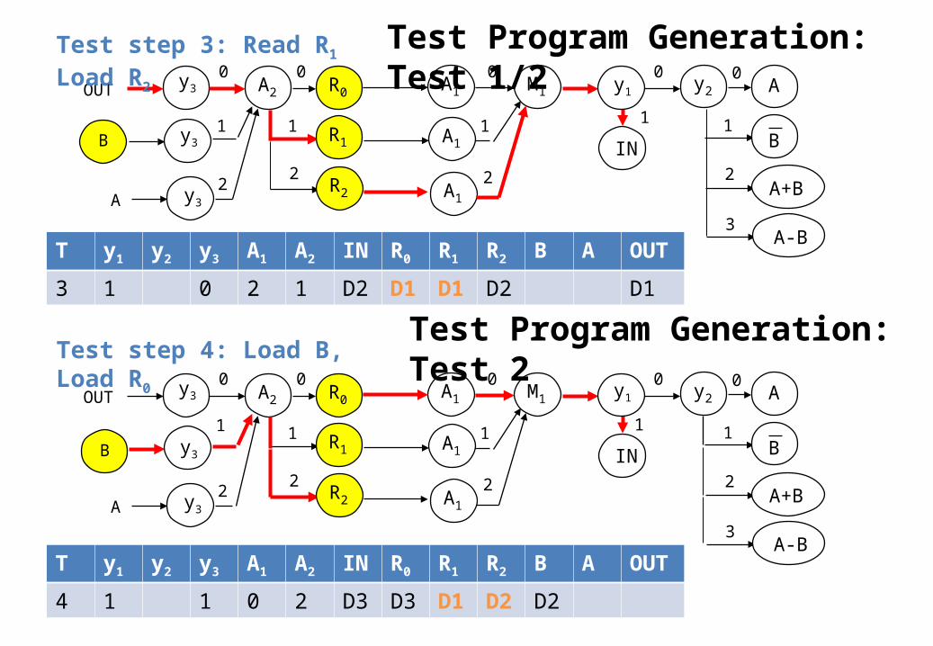
Test step 3: Read R1 Load R2Test Program Generation: Test 1/2
Test Program Generation: Test 2Test step 4: Load B, Load R0

0OUT y3 A2 R0
y3B R1
R2
1
2
0
1
0M1A1
A1
A1
1
2
y1
0
IN
0y2 A
B
A+B
1
2
A-B3
1
A y3
2
0OUT y3 A2 R0
y3B R1
R2
1
2
0
1
0M1A1
A1
A1
1
2
y1
0
IN
0y2 A
B
A+B
1
2
A-B3
1
A y3
2
T y1 y2 y3 A1 A2 IN R0 R1 R2 B A OUT
5 0 1 0 1 1 D3 D2 D2 D2 D2
T y1 y2 y3 A1 A2 IN R0 R1 R2 B A OUT
6 0 2 2 0 2 D5 D2 D2 D2 D2
Test Program Generation: Test 2Test step 5: Testing ALU (M1 = B), Transfer M1 to R1 , Read R1
Test 3Test step 6: Testing ALU (M1 = A+B), Transfer M1 to R0

0OUT y3 A2 R0
y3B R1
R2
1
2
0
1
0M1A1
A1
A1
1
2
y1
0
IN
0y2 A
B
A+B
1
2
A-B3
1
A y3
2
0OUT y3 A2 R0
y3B R1
R2
1
2
0
1
0M1A1
A1
A1
1
2
y1
0
IN
0y2 A
B
A+B
1
2
A-B3
1
A y3
2
T y1 y2 y3 A1 A2 IN R0 R1 R2 B A OUT
7 1 0 1 0 D4 D5 D4 D2 D2 D5
T y1 y2 y3 A1 A2 IN R0 R1 R2 B A OUT
8 0 3 2 2 2 D5 D4 D6 D2 D4
9 0 2 D6
Test Program Generation: Test 2/3Test step 7: Read R0 Load R1
Test step 8: Testing ALU (M1 = A-B), Transfer M1 to R2 Test step 9: Read R02
Test 4

Test step
Control part Data part
y1 y2 y3 A1 A2 IN R0 R1 R2 B A OUT
1 1 0 D1 D1
2 0 0 2 1 0 D1 D1
3 1 0 2 1 D2 D2 D1
4 1 1 0 2 D3 D3 D2
5 0 1 0 1 1 D2 D2
6 0 2 2 0 2 D5 D2
7 1 0 1 0 D4 D4 D5
8 0 3 2 2 2 D6 D4
9 0 2 D6
Fault cove-rage
2/2 4/4 3/3 3/3 3/3 4 3 3 2 1 3 4
Full Test Program and High Level Fault Table
0M1A1
A1
A1
1
2
y1
0
IN
0y2 A
B
A+B
1
2
A-B3
1
0OUT y3 A2 R0
y3B R1
R2
1
2
0
1
A y3
2
0OUT y3 A2 R0
y3B R1
R2
1
2
0
1
A y3
2
T y1 y2 y3 A1 A2 IN R0 R1 R2 B A OUT
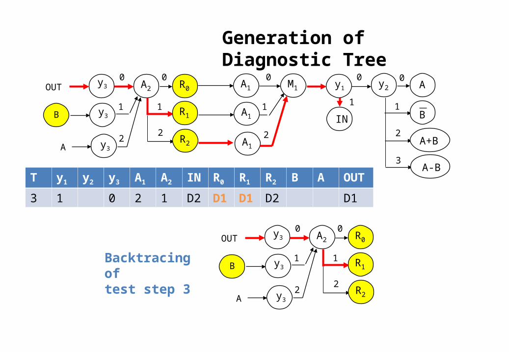
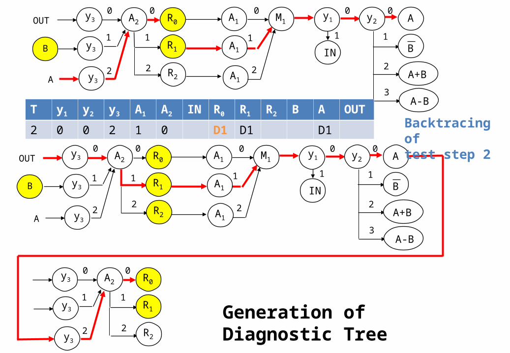
3 1 0 2 1 D2 D1 D1 D2 D1
Generation of Diagnostic Tree
Backtracing of test step 3
OUT
B
0M1A1
A1
A1
1
2
y10
IN
0y2 A
B
A+B
1
2
A-B3
1
A
0y3 A2 R0
y3 R1
R2
1
2
0
1
y3
2
0OUT y3 A2 R0
y3B R1
R2
1
2
0
1
A y3
2
0M1A1
A1
A1
1
2
y10
IN
0y2 A
B
A+B
1
2
A-B3
1
T y1 y2 y3 A1 A2 IN R0 R1 R2 B A OUT
2 0 0 2 1 0 D1 D1 D1
0y3 A2 R0
y3 R1
R2
1
2
0
1
y3
2
Generation of Diagnostic Tree
Backtracing of test step 2

0OUT y3 A2 R0
y3B R1
R2
1
2
0
1
A y3
2
0M1A1
A1
A1
1
2
y10
IN
0y2 A
B
A+B
1
2
A-B3
1
0y3 A2 R0
y3 R1
R2
1
2
0
1
y3
2
0M1A1
A1
A1
1
2
y1
0
IN
0y2 A
B
A+B
1
2
A-B3
1
Generation of Diagnostic TreeBacktracing of test step 1
Time frame 3 Time frame 2
Time frame 1

Research in ATI© Raimund Ubar
47
OP
LDA 0 AC=M
AND 1 AC=ACM
ADD 2 AC=ACM
SUB 3 AC=ACM
JMP 4 PC=A
STA 5 M=AC
JSR 6PC=A Jump to
subroutine
Parwan: Instruction Set
OP I P
CLA 7 0 1 AC=0
CMA 7 0 2 AC= AC
CMC 7 0 4 C= C
ASL 7 0 8 AC=2AC
ASR 7 0 9 AC=AC/2
BRA_N 7 1 0 If negative
BRA_Z 7 1 2 If zero
BRA_C 7 1 4 If carry
BRA_V 7 1 8 If overflow

Research in ATI© Raimund Ubar
PC_AP1 OP1
A1
PC_A + 2
P2 N A2
I 0
1
0 4,6
0-3, 5
7
7OP3
10
PC_A + 1OP27
PC_A
6
Z
C
V
PC_A + 2
2
4
8
0
0
0
0
1
1
1
Next PC offset calculation
Instruction addressingOP. I. P
LOC(PC_A)0-2550-15
PC_P PC_A
ALOC(PC_A+1)
0-2550-15PC_P PC_A
PC_POP1 P1
4
PC_P
Next memory page calculation
ALU FlagsOP
N
I
0 - 3
07
NFN(AC,M’)
P2,8,9
Fc2(AC)
C
V
OP
C
I
2,3
07
Fc1(AC,M’)
P4,8
Fc2(AC)
OP
V
I
2,3
07
Fv1(AC,M’)
P8
Fv2(AC)
OP
Z
I
0 - 3
07
ZFz(AC,M’)
P2,8,9
Fc2(AC)
Output behaviourM’ (A)
OP5
AC
M’P A LOC(A)
0-2550-15
Direct addressing
LOC(M’)
PM’’
M’
0-15
Indirect addressing
ALU Data PathAC
P1 OP1 M’
AC & M’
AC + M’
AC - M’
AC
P3 0
I
OP3
0
1
M’’
0
0 0
1
2
3
7OP2
1
AC
AC/2
2
8
9
AC
2AC
4 AC
Parwan: HLDD Model
Research in ATI© Raimund Ubar
49
OP
N
I
0 - 3
07
NFN(AC,M’)
P2,8,9
Fc2(AC)
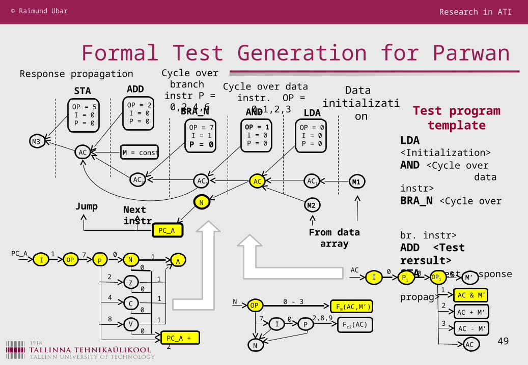
Formal Test Generation for Parwan
Test program template
LDA <Initialization>
AND <Cycle over data instr>BRA_N <Cycle over br. instr>ADD <Test rersult>STA <Test response propag>
ACP1
OP1 M’
AC & M’
AC + M’
AC - M’
AC
I0 0 0
1
2
3
PC_AP N AI
1 7OP 10
Z
C
V
PC_A + 2
2
4
8
0
0
0
0
1
1
1
OP = 5I = 0P = 0
AC
STA
AC2
M = const
OP = 2I = 0P = 0
ADD
OP = 7I = 1
P = 0
BRA_N
N
AC1
PC_A
Next instr
Jump
OP = 1I = 0P = 0
AND
AC
OP = 0I = 0P = 0
LDA
M2
AC1 M1
M3
From data array
Cycle over branch instr P = 0,2,4,6
Cycle over data instr. OP = 0,1,2,3
Data initialization
Response propagation

Research in ATI© Raimund Ubar
50
Test Program for Parwan Microrocessor
FOR VAR1 = 0, 1, 2, 4, 8, 9 (For all single byte ALU instructions) FOR VAR2 = 0, 2, 4,… N (For all data operands)
FOR VAR3 = 0, 2, 4, 8 (For all branch operations)
k) LDA, VAR2 (Data initialization)k+2) I=0, P=0, OP = VAR1 (ALU Test, Flag initialization)k+3) I=1, P=VAR3, OP=7 (Branch Test)k+4) m (Jump address for fixing AC1 = AC)k+5) ADD, CONST (Fixing AC2 AC1)k+7) ADD, LOC (REF) (Signature calculated: REF = REF + AC1)k+9) STA, LOC (REF) (Finish: Signature updated)
END VAR3 END VAR2END VAR1
m) ADD, LOC (REF) (Signature calculated: REF = REF + AC2)m+2) JMP, k+9
![Untitled-2 [talenttraininginstitute.com]...2020/12/03 · Level 2 — Level 2 Level 2 — Level 2 — Level 2 — Level 2 — Level 2 — Level 2 — Level 3 — Level 3 — Level](https://cdn.vdocuments.us/doc/165x107/60a851c8c991bb3fe20f48c7/untitled-2-tal-20201203-level-2-a-level-2-level-2-a-level-2-a.jpg)


