ES51063 1/2 DIGIT A/D CONVERTER W/LCD
03/05/141
1. GENERAL DESCRIPTION
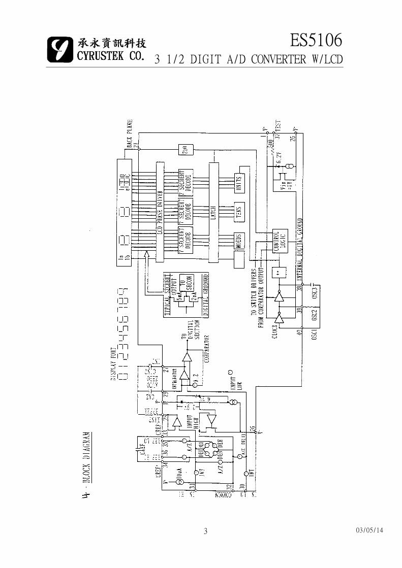
The ES 5106 is a low power monolithic CMOS 3 1/2 digit LCD
display A/D converter. The single chip ES 5106 provides all necessary
active devices which contains the internal clock, voltage reference, seven-
segment decoders, LCD display drivers and a back plane driver. The
improved internal zener reference voltage circuit gives the analog
common a small temperature coefficient of 60 ppm/℃ typically.
The high accuracy characteristics of the ES5106 perform very low
linearity error and rollover error. The high input impedance (>1012Ω) and
low input leakage current (1pA typical) give the ES5106 a good
application in the field of high impedance circuit measurement. The
differential input and reference are suitable for measuring bridge
transducer or ohms by using ratiometric method.
The dual slope conversion technique makes the ES5106 a good
normal and common mode rejection ratio. With a suitable oscillator
frequency, the ES5106 has a high rejection of 50HZ, 60HZ and 400HZ
line frequency noise.
With single power supply, a few passive components and a LCD
display, ES5106 can be built as a high performance panel meter. Existing
TSC7106 or ICL7106 based systems may be upgraded without changing
external, passive component values.
ES51063 1/2 DIGIT A/D CONVERTER W/LCD
03/05/142
2. FEAUTRES
Guaranteed zero reading with zero input
Low input leakage current (1pA typical)
Internal Reference with low temperature drift (60ppm/℃ typial)
Low noise (15μVp-p typical)
Direct LCD display driver-no external components required
Differential input and voltage reference
Precision null detection with true polarity at zero
Internal clock circuit
No additional active circuits required
3. APPLICATIONS
Digital panel meters
Digital multimeters
Thermometers
Capacitance meters
pH meters
Photometers
ES51063 1/2 DIGIT A/D CONVERTER W/LCD
03/05/143
E T
ES51063 1/2 DIGIT A/D CONVERTER W/LCD
03/05/144
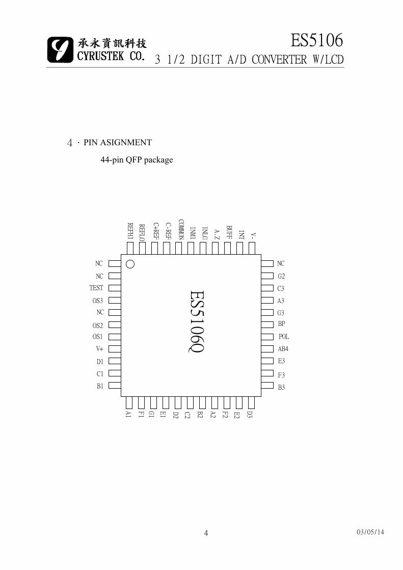
4. PIN ASIGNMENT
44-pin QFP package
NC
NC
TEST
OS3
OS2
OS1
V+
D1
C1
B1
F1
G1
E1 D2
C2
B2
A2
F2 E2
D3
B3
F3
E3
AB4
POL
BP
G3
A1
NC
NC
A3
C3
G2
V-
INT
BUFF
A.Z
INLO
INMI
COMM
ON
C-RE
F
C+RE
F
REFL
O
REFH
I
ES5106
Q

ES51063 1/2 DIGIT A/D CONVERTER W/LCD
03/05/145
PIN ASSIGNMENT
40-pin DIP package
ES51063 1/2 DIGIT A/D CONVERTER W/LCD
03/05/146
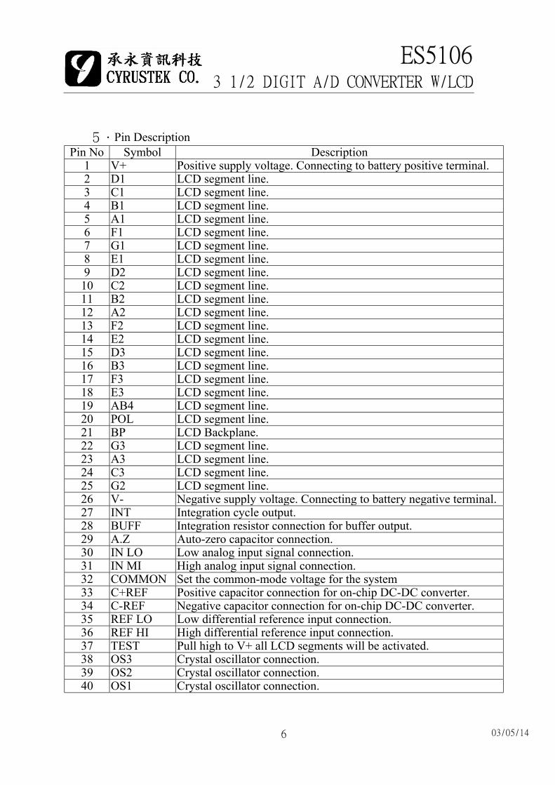
5.Pin DescriptionPin No Symbol Description
1 V+ Positive supply voltage. Connecting to battery positive terminal. 2 D1 LCD segment line. 3 C1 LCD segment line. 4 B1 LCD segment line. 5 A1 LCD segment line. 6 F1 LCD segment line. 7 G1 LCD segment line. 8 E1 LCD segment line. 9 D2 LCD segment line. 10 C2 LCD segment line. 11 B2 LCD segment line. 12 A2 LCD segment line. 13 F2 LCD segment line. 14 E2 LCD segment line. 15 D3 LCD segment line. 16 B3 LCD segment line. 17 F3 LCD segment line. 18 E3 LCD segment line. 19 AB4 LCD segment line. 20 POL LCD segment line. 21 BP LCD Backplane. 22 G3 LCD segment line. 23 A3 LCD segment line. 24 C3 LCD segment line. 25 G2 LCD segment line. 26 V- Negative supply voltage. Connecting to battery negative terminal. 27 INT Integration cycle output. 28 BUFF Integration resistor connection for buffer output. 29 A.Z Auto-zero capacitor connection. 30 IN LO Low analog input signal connection. 31 IN MI High analog input signal connection. 32 COMMON Set the common-mode voltage for the system 33 C+REF Positive capacitor connection for on-chip DC-DC converter. 34 C-REF Negative capacitor connection for on-chip DC-DC converter. 35 REF LO Low differential reference input connection. 36 REF HI High differential reference input connection. 37 TEST Pull high to V+ all LCD segments will be activated. 38 OS3 Crystal oscillator connection. 39 OS2 Crystal oscillator connection. 40 OS1 Crystal oscillator connection.

ES51063 1/2 DIGIT A/D CONVERTER W/LCD
03/05/147
6.ABSOLUTE MAXIMUM RATINGE
Characteristic Rating
Supply Voltage (V+ to V-) 12V
Analog Input Voltage (either input) V+ to V-
Reference Input Voltage (either input) V+ to V-
Clock Input TEST to V+
Power Dissipation (plastic package) 800mW
Operating Temperature 0℃ to +70℃
Storage Temperature -65℃ to +160℃
Lead Temperature(soldering, 10 sec) 270℃
7.ELECTRICAL CHARACTERISTICS
LimitCharacteristic Test Condition
Min. Typ. Max.Units
Zero Input Reading VIN=0.0V
Full-Scale=200.0mV-000.0 ±000.0 +000.0
Digital Reading
Ratiometric Reading VIN=VREF, VREF=100mV 999 999/1000 1000 Digital Reading
Linearity
(Max. deviation from
best straight line fit)
Full-Scale=200mV
or Full-Scale=2.000V
-1 ±0.2 1 Counts
ES51063 1/2 DIGIT A/D CONVERTERW/LCD
03/05/148
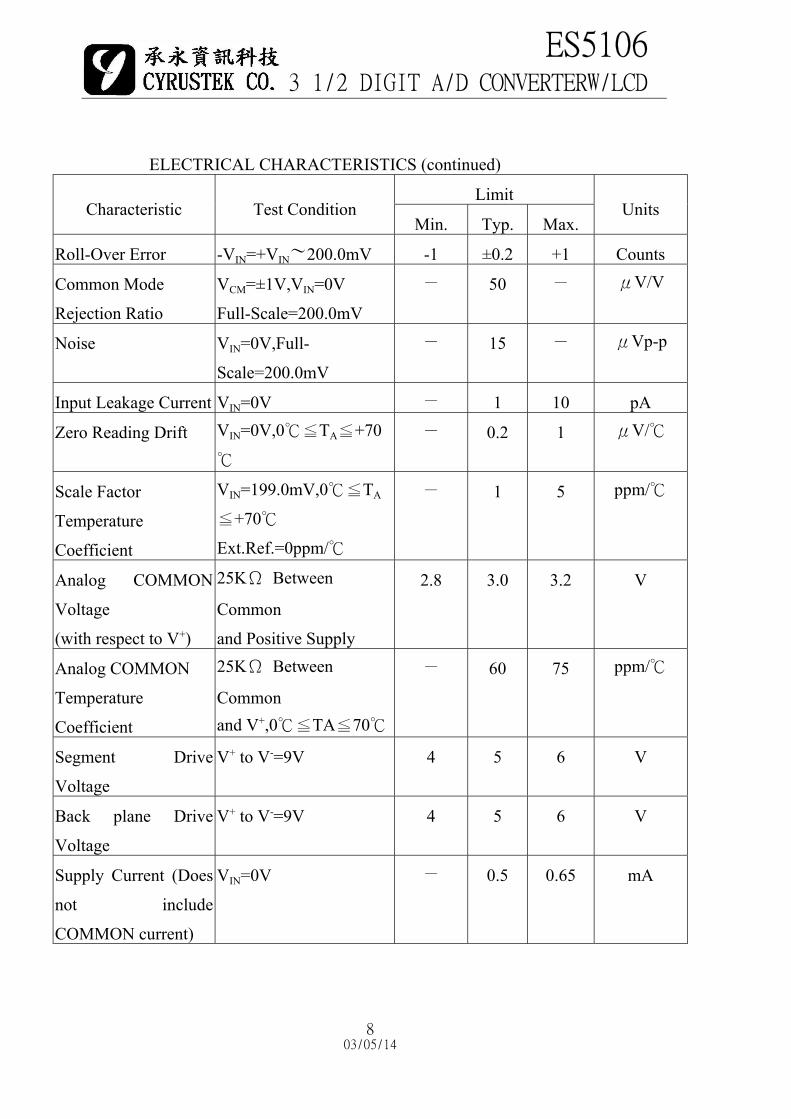
ELECTRICAL CHARACTERISTICS (continued)
LimitCharacteristic Test Condition
Min. Typ. Max.Units
Roll-Over Error -VIN=+VIN〜200.0mV -1 ±0.2 +1 Counts
Common Mode
Rejection Ratio
VCM=±1V,VIN=0V
Full-Scale=200.0mV
- 50 - μV/V
Noise VIN=0V,Full-
Scale=200.0mV
- 15 - μVp-p
Input Leakage Current VIN=0V - 1 10 pA
Zero Reading Drift VIN=0V,0℃≦TA≦+70
℃
- 0.2 1 μV/℃
Scale Factor
Temperature
Coefficient
VIN=199.0mV,0℃≦TA
≦+70℃
Ext.Ref.=0ppm/℃
- 1 5 ppm/℃
Analog COMMON
Voltage
(with respect to V+)
25KΩ Between
Common
and Positive Supply
2.8 3.0 3.2 V
Analog COMMON
Temperature
Coefficient
25KΩ Between
Commonand V+,0℃≦TA≦70℃
- 60 75 ppm/℃
Segment Drive
Voltage
V+ to V-=9V 4 5 6 V
Back plane Drive
Voltage
V+ to V-=9V 4 5 6 V
Supply Current (Does
not include
COMMON current)
VIN=0V - 0.5 0.65 mA

ES51063 1/2 DIGIT A/D CONVERTER W/LCD
03/05/149
8.Operation Mode
Analog Common
The Common pin is used to set the common-mode voltage for
the system in which the input signals are floating with respect to the
power supply of the ES5106. In all most of the applications, IN LO,
REF LO and COMMON pins are tied to the same point, so that the
common mode voltage can be removed from the reference system
and the converter. In some applications, IN LO may not at the same
point with COMMON and thus a common mode voltage exists in
the system, the high CMRR (86db typical) of the ES 5106 can take
care of this common mode voltage. Neverthereless, it should be care
to prevent the output of the integrator from saturation.
The COMMON pin is also used as a voltage reference. It sets a
voltage which is around 2.9 volts more negative than the positive
supply. The COMMON voltage of ES5106 has a 0.001 %/% voltage
coefficient and a low output impedance of 15Ω typical.
The analog COMMON is tied internally to an N channel FET
capable of sinking 30mA. This FET will hold the COMMON
voltage at 2.9 volts when an external load attempt to pull the
COMMON voltage toward the positive supply.

ES51063 1/2 DIGIT A/D CONVERTER W/LCD
03/05/1410
The source current of COMMON is only 10μA, so it is easy to
pull COMMON voltage to a more negative voltage with respect to
the positive supply.
When the total supply voltage is large enough to cause the
zener to regulate(>7V), the COMMON voltage will have a low
temperature cofficient typically less than 60 ppm/℃. This voltage
can be used to generate the ES5106 reference voltage and an
external voltage reference will be unnecessary in most cases.
Reference Voltage
For a 1000 counts reading, the input signal must be equal to the
reference voltage. So for a 2000 counts full-scale reading, it requires
the input signal be twice the reference voltage. Thus, for the 200mV
and 2.000V full-scale, the reference voltage should equal 100.0mV
and 1.000V, In some applications the full-scale input voltage may be
other than 200mV or 2V, but 600mV, for example, The reference
voltage should be set to 300 mV and the input signal can be used
directly without being divided.
The differential reference can be used during the measurment
of resistor by the ratiometric method and when a digital reading of
zero is desired for VIN≠0. A compensating offset voltage can be
applied between COMMON and IN LO and the voltage of being
measured is connected between COMMON and IN HI.
ES51063 1/2 DIGIT A/D CONVERTER W/LCD
03/05/1411
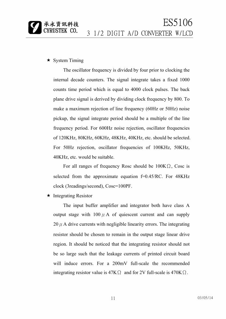
System Timing
The oscillator frequency is divided by four prior to clocking the
internal decade counters. The signal integrate takes a fixed 1000
counts time period which is equal to 4000 clock pulses. The back
plane drive signal is derived by dividing clock frequency by 800. To
make a maximum rejection of line frequency (60Hz or 50Hz) noise
pickup, the signal integrate period should be a multiple of the line
frequency period. For 600Hz noise rejection, oscillator frequencies
of 120KHz, 80KHz, 60KHz, 48KHz, 40KHz, etc. should be selected.
For 50Hz rejection, oscillator frequencies of 100KHz, 50KHz,
40KHz, etc. would be suitable.
For all ranges of frequency Rosc should be 100KΩ, Cosc is
selected from the approximate equation f=0.45/RC. For 48KHz
clock (3readings/second), Cosc=100PF.
Integrating Resistor
The input buffer amplifier and integrator both have class A
output stage with 100μA of quiescent current and can supply
20μA drive currents with negligible linearity errors. The integrating
resistor should be chosen to remain in the output stage linear drive
region. It should be noticed that the integrating resistor should not
be so large such that the leakage currents of printed circuit board
will induce errors. For a 200mV full-scale the recommended
integrating resistor value is 47KΩ and for 2V full-scale is 470KΩ.

ES51063 1/2 DIGIT A/D CONVERTER W/LCD
03/05/1412
Integrating Capacitor
The integrating capacitor should be selected to maximize
integrator output voltage swing without causing output saturation. If
the analog COMMON is used as voltage reference, a±2V full-scale
integrator output swing is satisfactory. For 3 readings/second
(48KHz clock) a 0.22μF value of CINT is suggested. When different
oscillator frequencies are used, CINT must be changed in inverse
proportion to maintain the nominal ±2V integrator swing.
The integrating capacitor should have low dielectric absorption
to minimize roll-over error. An inexpensive polypropylene capacitor
will work well.
Auto-Zero Capacitor
The auto-zero capacitor size has some influence on system
noise. A 0.47μF capacitor is recommended for 200mV full scale
where noise is very important. A 0.047μF capacitor is adequate for
2V full scale aplications. A mylar type dielectric capacitor is
adequate.
Reference Voltage Capacitor
When IN LO is tied to analog COMMON, a 0.1μF capacitor
adequate to be the reference capacitor. If a large common-mode
voltage exists and the application require a 200mV full scale, a
larger value is required to prevent roll-over error. A 1.0μF
capacitor will hold the roll-over error to 0.5 count.
ES51063 1/2 DIGIT A/D CONVERTER W/LCD
03/05/1413
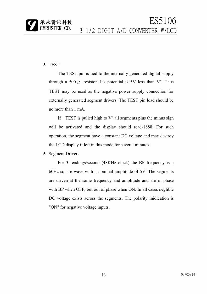
TEST
The TEST pin is tied to the internally generated digital supply
through a 500Ω resistor. It's potential is 5V less than V+. Thus
TEST may be used as the negative power supply connection for
externally generated segment drivers. The TEST pin load should be
no more than 1 mA.
If TEST is pulled high to V+ all segments plus the minus sign
will be activated and the display should read-1888. For such
operation, the segment have a constant DC voltage and may destroy
the LCD display if left in this mode for several minutes.
Segment Drivers
For 3 readings/second (48KHz clock) the BP frequency is a
60Hz square wave with a nominal amplitude of 5V. The segments
are driven at the same frequency and amplitude and are in phase
with BP when OFF, but out of phase when ON. In all cases neglible
DC voltage exists across the segments. The polarity inidication is
"ON" for negative voltage inputs.

ES51063 1/2 DIGIT A/D CONVERTER W/LCD
03/05/1414
9.TEST CIRCUIT
ES51063 1/2 DIGIT A/D CONVERTER W/LCD
03/05/1415
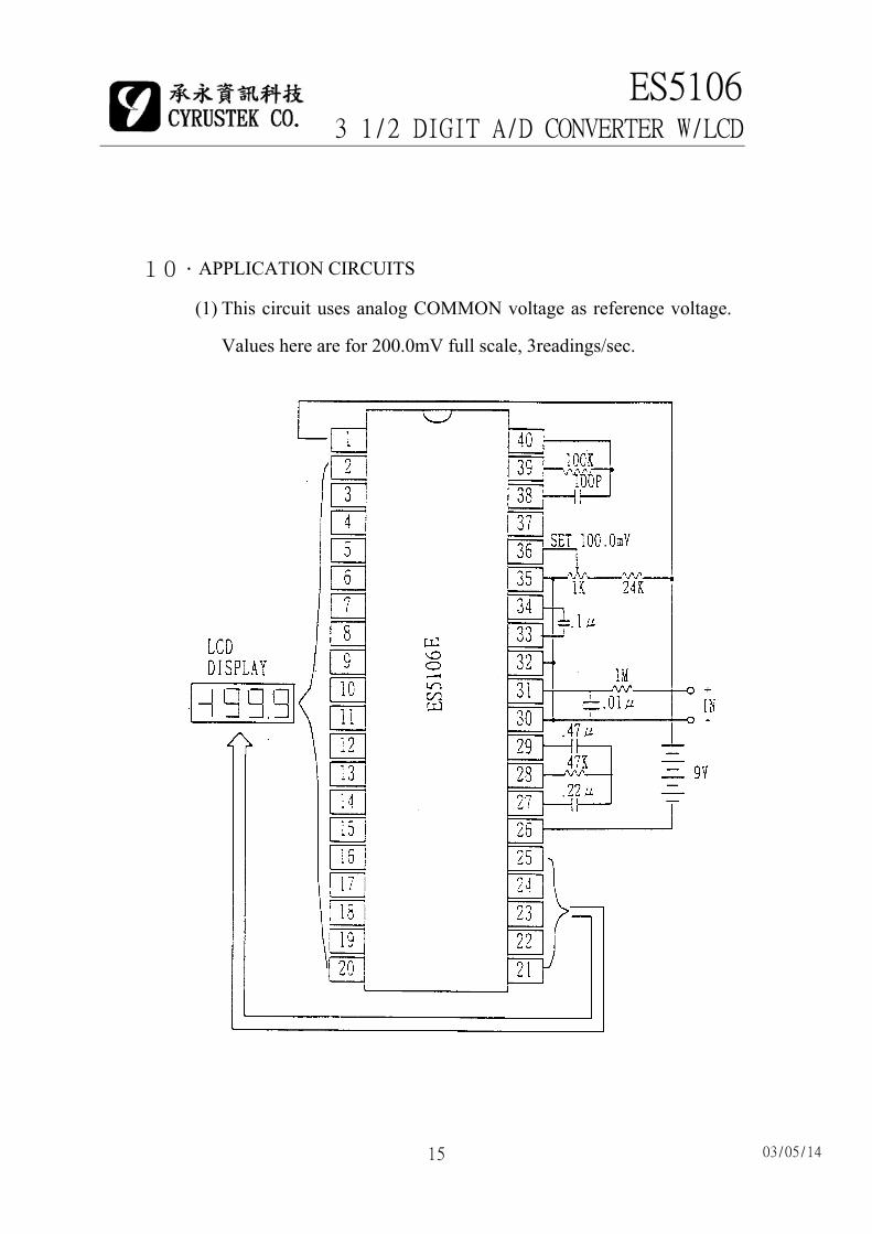
10.APPLICATION CIRCUITS
(1) This circuit uses analog COMMON voltage as reference voltage.
Values here are for 200.0mV full scale, 3readings/sec.

ES51063 1/2 DIGIT A/D CONVERTER W/LCD
03/05/1416
(2) The values of this circuit are for 2.000V full scale, 3 readings/sec.
ES51063 1/2 DIGIT A/D CONVERTER W/LCD
03/05/1417
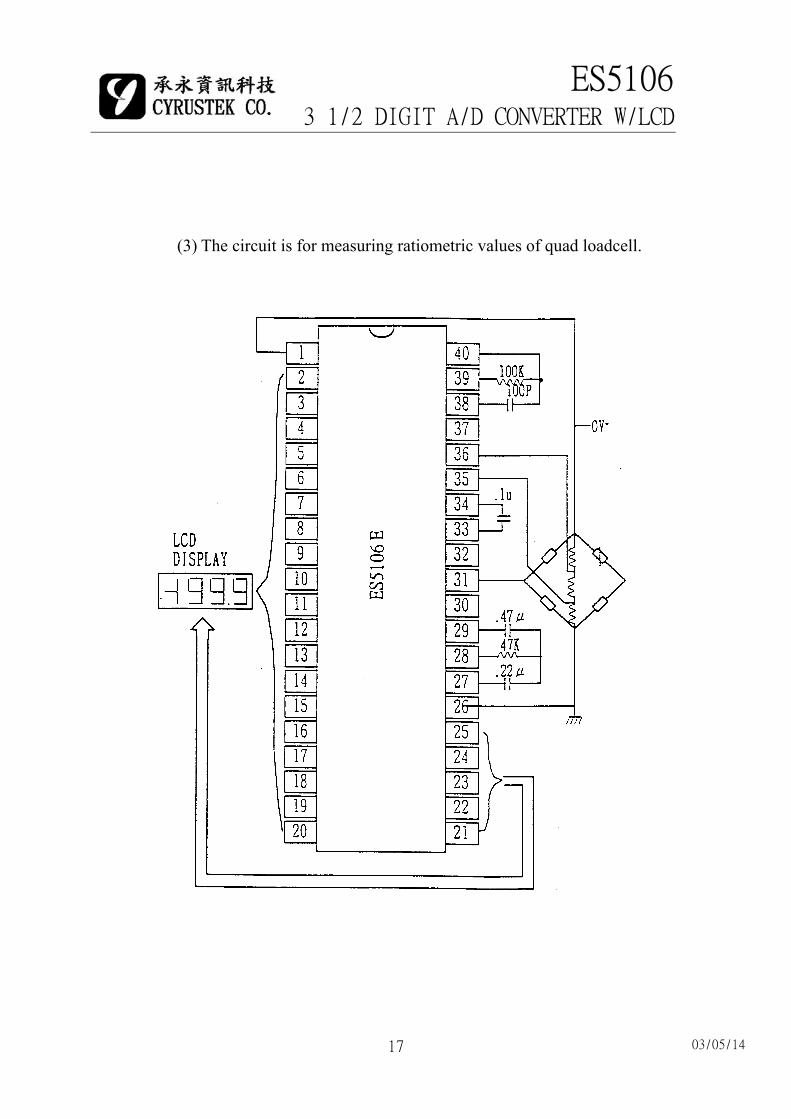
(3) The circuit is for measuring ratiometric values of quad loadcell.

ES51063 1/2 DIGIT A/D CONVERTER W/LCD
03/05/1418
(4) This circuit is a digital centigrade thermometer. The temperature
sensor is a silicon diode-connected transistor which has a
temperature coefficient of about-2mV/℃.

ES51063 1/2 DIGIT A/D CONVERTER W/LCD
03/05/1419
11.包裝(Package)
44-pin QFP package

ES51063 1/2 DIGIT A/D CONVERTER W/LCD
03/05/1420
40-pin DIP package


