
www.sciencemag.org/content/344/6179/70/suppl/DC1
Supplementary Material for
Soft Microfluidic Assemblies of Sensors, Circuits, and Radios for the Skin
Sheng Xu, Yihui Zhang, Lin Jia, Kyle E. Mathewson, Kyung-In Jang, Jeonghyun Kim, Haoran Fu, Xian Huang, Pranav Chava, Renhan Wang, Sanat Bhole, Lizhe Wang, Yoon Joo Na, Yue Guan, Matthew Flavin, Zheshen Han, Yonggang Huang,* John A. Rogers*
*Corresponding author. E-mail: [email protected] (J.A.R.); [email protected] (Y.H.)
Published 4 April 2014, Science 344, 70 (2014)
DOI: 10.1126/science.1250169
This PDF file includes:
Materials and Methods
Figs. S1 to S29
Tables S1 to S3
Full Reference List Other Supplementary Material for this manuscript includes the following: (available at www.sciencemag.org/content/344/6179/70/suppl/DC1)
Movies S1 and S2

2
Materials and Methods
Design rationale for the circuits
For the inductive electrocardiogram (ECG) system, Chip 105 (10 µF capacitor) is
used to block the DC offset of the incoming ECG signal. Chip 107 (0.1 µF capacitor) and
chip 13 (200 kΩ) form a high pass resistor-capacitor filter to remove low frequency noise
from the incoming ECG signal. The instrumentation amplifier (AD627b, chip 1)
amplifies the ECG signal by 800 times. Chip 107 (0.1 µF capacitor) and chip 10(10 kΩ)
form a low pass resistor-capacitor filter to remove high frequency noise from the
amplified ECG signal collected by the epidermal working and reference electrodes, with
a floating ground. A voltage controlled oscillator (MAX2750, chip 3) generates high
frequency signals at ~2.4 GHz that represent the ECG signal voltage. The output of this
chip passes out of the device through a compact three dimensional antenna (chip 18). A
separate patch antenna, radiofrequency (RF) amplifier and frequency counter can receive
the transmitted RF wave reliably at a distance of up to 1 m, when operated in a room
designed to eliminate background electrical noise. The inductive power module is based
on resonant inductive coupling: a 10 µH inductive coil (27T103C, chip 101) and 0.1uF
capacitor (chip 107) forms an inductor-capacitor loop. A Schottky diode provides
rectification and a capacitor (10 F) provides integration.
For the multifunctional device, the electrophysiological (EP) amplification subunit is
similar to that of the ECG system. The acceleration sensing module consists of chip 6
(KXTH9) which converts acceleration to an analog voltage output. The temperature
sensing module uses a Wheatstone bridge circuit to convert temperature to an analog
voltage output. Chip 5 (PTS080501B500RP100) is a resistance temperature detector.
Chips 16 and 17 are paired resistors to form the bridge loop. In the multiplexing module,
chip 21 (LTC6991) generates an oscillating signal that controls the multiplexer
(MAX4734, chip 2), to switch sequentially among the outputs of the three sensor
channels, EP, temperature and acceleration sensing, to allow data transmission with a
single voltage controlled oscillator. In particular, data from the EP, acceleration and
temperature channels transmit for 18, 9 and 9 seconds, respectively, as determined by two
oscillators that generate two bit control logic by tuning the ratio of their oscillation
frequencies to 1:2. A pulse width modulation oscillator periodically turns on and off the
voltage controlled oscillator, for a duty cycle of ~7% at a frequency of 1000 Hz, to
reduce the average power consumption from ~40 mW (continuous operating mode) to
~6.3 mW. The wireless data transmission subunit is similar to that of the ECG system.
Molding structures of surface relief on the elastomeric device substrate
The process began with a piece of a clean (100) Si wafer, coated with a 100 nm
thick Si3N4 film formed by plasma enhanced chemical vapor deposition (STS PECVD).
Photolithography (AZ P4620, 3000 rpm, 30 s, soft bake at 110 °C for 3 min, 300 mJ/cm2,
1:2 volume ratio of AZ 400K and de-ionized water for 1 min) and reactive ion etching
(RIE, 22.5 sccm CF4, 40 mT, 150 W, 8 min) defined an array of circles (20 m ) in the
Si3N4. Wet chemical anisotropic etching of the silicon with KOH (100 ml 33% weight
percent water solution, 20 ml isopropanol alcohol, 130 °C, 45 min, with strong magnetic
stirring) generated an array of pyramidal shaped recessed regions on the surface of the
wafer. After removing the remaining Si3N4, a second photolithography step (AZ P4620)

3
and inductively coupled plasma reactive ion etching process (ICP RIE, Bosch process)
defined trenches (30 m in depth) for the support posts for the chips. A third
photolithography step (AZ P4620) and RIE process (STS ICP RIE, Bosch process)
defined the trenches (100 m in depth) for the isolation barriers. A layer of
polytetrafluoroethylene (~200 nm) conformally deposited (STS ICP RIE) all exposed
surfaces to minimize adhesion. Thin (300 µm) silicone substrates (Ecoflex, Smooth-On)
were prepared by mixing the two components of a commercial kit in a 1:1 weight ratio,
spin-casting (300 rpm for 30 s) the resulting material onto the processed Si wafer and
then curing into a solid form (2 hours at room temperature).
Fabrication of the interconnect network
The process began with spin casting of polydimethylsiloxane (PDMS, Sylgard 184),
mixed at 10:1 ratio, onto a clean glass slide at 3000 rpm for 30 s. After curing in an oven
at 70 °C for 2 hours, the PDMS was exposed to oxygen plasma (20 sccm O2, 300 mT,
200 W, 30 s). A 2.4 m thick layer of polyimide (PI, from poly(pyromellitic dianhydride-
co-4,4′-oxydianiline) amic acid solution was then applied by spin casting (2000 rpm for
60 s), baked on a hotplate at 150 °C for 4 mins and in a vacuum oven at 10 mT and 250
°C for 1 h. The interconnects and metal electrodes consisted of a 400 nm thick layer of
Cu deposited by electron beam evaporation onto the PI. Photolithography (AZ P4620)
and etching (CE-100 copper etchant, Transene Company) defined patterns in the Cu.
Next, spin coating formed a second 2.4 m thick layer of PI over the entire structure. A
50 nm thick layer of SiO2 was then deposited using electron beam evaporation, to serve
as an etching mask for the PI. Next, photolithography (AZ P4620), RIE etching (50 mT,
40 sccm CF4, 100 W, 20 min), and oxygen plasma etching (20 sccm O2, 300 mT, 200 W
for 21 mins) patterned the layers of PI in a geometry matched to the metal traces. The
residue SiO2 mask was removed using buffered oxide etchant, and the overall circuit
electrodes were immersed in electroless Sn plating solution (Transene Company) at 80
°C for ~10 s. The Sn deposited only onto the exposed Cu surfaces, for the purpose of
ensuring good wettability of the solder on the bonding pads. Finally, the circuit electrodes
were retrieved using water soluble tape (3M, Inc.) for aligned transfer to the device
substrate.
Assembly of the chip components
Electron beam evaporation of Ti (5 nm) / SiO2 (50 nm) on the pads (mounting sites
for the chips) of the interconnect network formed backside coatings (30). A shadow mask
made of PI (Stencilunlimited corp.) with patterns matched to the support posts, was
aligned and laminated onto the molded silicone substrate (thickness ~0.4 mm). The
substrate was then activated by exposure to ultraviolet induced ozone for 5 mins.
Aligning and laminating the interconnect network onto this surface led to an irreversible
strong bonding upon contact, only at the locations of the support posts (~1 mm diameter).
After aging for 10 mins, the water soluble tape was removed by immersion in tap water
for 1 hour. Another shadow mask, the same as the one for electroless Sn plating, was then
aligned and laminated onto the electrodes to selectively expose the contact pads for the
pin contacts associated with each of the component chips. A Sn42Bi58 alloy solder paste
(Chip Quik Inc. SMDLTFP250T3) was screen printed onto the contact pads. A combined
lapping and polishing process with tripod polisher was used for thinning of the thickest

4
chips, such that all chips had thicknesses <1 mm. The lapping process involved a fast
back grinding step, followed by a polishing process to remove remaining rough surfaces.
Each chip component was manually placed over the electrodes under an optical
microscope. After all of the chips were in position, the solder paste was reflowed in an
oven at ~180 °C for 5 mins. Good solder joints appeared smooth and shiny, with
complete wetting to the contact pads. A thin silicone superstrate (~100 m thick)
encapsulated the entire chip region of the device. The edges were sealed with an
additional application of partially cured silicone followed by baking on a hotplate at 120
°C for 10 min. A liquid PDMS base (Sylgard 184, without the curing agent), injected into
the capped cavity through an edge, covered all of the chips and interconnects via
capillary force.
Mechanical testing and simulation of the devices
An array of metal dots (100 nm Cr, 0.4 mm for each dot, 1 mm pitch) was
deposited through a polyimide shadow mask mounted on the back side of the relief
substrate. After integrating the interconnect network and chips and adding a thin layer of
PDMS base, equal-biaxial stretching was applied to the device using a customized stage.
Strain was added/removed gradually and simultaneously in both directions. Images of the
device at various stages of deformation were collected with a digital single-lens reflex
camera from the backside the device so that the metal dots were clearly visible. The
Young’s moduli of the devices with and without the chips and interconnect network were
measured in orthogonal directions using an INSTRON MINI44. The strain-stress curves
were averaged over at least three individual measurements. Mechanical simulation was
performed using finite element analysis (FEA) techniques.
Full three-dimensional (3D) FEA was adopted to analyze the postbuckling behaviors
of the entire device under uniaxial and biaxial stretching. The chips were selectively
bonded to the silicone substrate (Ecoflex; thickness 0.5 mm) via small circular (diameter
1 mm) and rectangular (0.5 mm by 1.0 mm) pedestals. Each of the metal interconnect
(Cu, thickness 400 nm) lines, was encased, top and bottom, by a thin layer of polyimide
(PI, thickness 2.4 µm for each layer). The elastic modulus (E) and Poisson’s ratio (ν) are
EEcoflex=0.0623 MPa and νEcoflex=0.49 for Ecoflex; ECu=119 GPa and νCu=0.34 for copper;
and EPI=2.5 GPa and νPI=0.34 for PI. Eight-node 3D solid elements and four-node shell
elements were used for the ecoflex and self-similar electrode, respectively, and refined
meshes were adopted to ensure the accuracy. Linear buckling analyses were carried out
to determine the critical buckling strain and lowest buckling mode for each interconnect,
which were then implemented as initial geometric imperfections in the postbuckling
simulation. The evolution of deformed configurations with applied strains were obtained
from FEA for the entire device under both uniaxial and biaxial stretchings, as shown in
Figs. 2, S11, S13, and S14. Good agreement between FEA and experiment results can be
found.
Functional testing of the devices on human subjects
All experiments on human were conducted under approval from Institutional
Review Board at the University of Illinois at Urbana-Champaign (protocol number:
13398). There are three subjects (age: 21–29, all males), co-authors in the paper.
Research was carried out with informed signed consents from the subjects. Prior to
5
device integration, hairs were removed and the skin was cleaned using a mild abrasive
and Scotch tape to exfoliate some of the stratum corneum and to remove sebaceous oils
(31). Afterwards, the device was placed on the desired areas on the skin for recording of
EP signals. For near field coupling powering, a high frequency alternating current source
(10 Vp-p at 150 kHz) to the primary coil was generated using a KEITHLEY 3390 50 MHz
arbitrary waveform generator. The input and output characteristics of the wireless coil
were measured using an Agilent infiniium DSO8104A oscilloscope (1 GHz, 4 channels).
The ECG data were received by a back end antenna, then filtered through a 2.2-2.7 GHz
band pass filter (RF-lambda, RBPF2450, SN: 12041902227), amplified by a 2.2-2.7 GHz
low noise amplifier (ZQL-2700MLNW+), and read out by a frequency counter, where the
frequency-modulated signals were processed and analyzed. For recordings with
commercial equipment, we used a pair of Au/Ag ring electrodes, fixed with an adhesive
sticker to the skin along with conductive electrode gel. A ground electrode was attached
on a more proximal section of the right arm. The wireless system, placed directly
adjacent to the electrodes used for measurement with the commercial system (Brain
Vision V-Amp, with a nearby ground electrode on a distal position on the left forearm),
utilized a floating ground. Recorded data were passed through band pass filters to remove
line noise and other high frequency artifacts, as well as slow drifts in the signal. The
mean voltage of each signal was subtracted to remove the DC offsets. The data were then
normalized to their peak values, to facilitate comparisons.

6
Fig. S1.
Optical image of the non-coring needle, highlighting the inject pore on the side wall
of the needle. This construction avoids removal of subject material during the injection
process. The elastomer self-seals after removal of the needle. Additional elastomer can be
added to enhance the robustness of this seal.

7
Fig. S2
Thermogravimetric analysis of 10.12 mg PDMS base fluid at elevated temperatures
for prolonged time.

8
Fig. S3
3D-FEA results that illustrate the mechanics advantage of free-floating
interconnects in comparison with fully bonded or embedded ones. (A) Initial
configuration of one of the interconnects shown in Fig. 1C; (B) the strain distribution of
the interconnect only with two ends bonded onto the top of the Ecoflex, when the applied
strain reaches the corresponding elastic stretchability (167%) of the interconnect; (C) the
strain distribution of the interconnect fully bonded onto the top of the Ecoflex, when the
applied strain reaches its elastic stretchability (17%); (D) the strain distribution of the
interconnect fully embedded in the middle of the Ecoflex, when the applied strain reaches
its elastic stretchability (8%).

9
Fig. S4
Characterization of the hierarchical substrate. (A) Optical image of a substrate with
multiple levels of embossed relief. (B) SEM image of a small region of the substrate to
illustrate its hierarchical structure.

10
Fig. S5
X-ray side view image of a typical commercial chip with standard package design. The thickness of this chip can be reduced to 0.86 mm by grinding the excessive
packaging epoxy away.

11
Fig. S6
Optical images of the interface wetting behavior of the interconnects. Chips bonded
on the interconnects (A) before and (B) after electroless Sn plating. These images clearly
show that after Sn plating, the Sn42Bi58 solder paste, applied by screen printing, can wet
the interconnector surfaces well and thus allow a robust bonding interface.

12
Fig. S7
Layout design of the single ECG system, with labels for different parts of the device. The design of the transition region between the interconnectors and the chip bonding
pads, to minimize stress concentration, is also highlighted in the dashed purple box.

13
Fig. S8
Comparison of mechanical performance of three different interconnect designs at
the point of the periphery of the microfluidic enclosure. (A) Schematic illustration
(left panel) of a self-similar serpentine interconnect across the interface, and the
distribution of maximum principal strain (middle panel for horizontal stretching along the
x direction; right panel for vertical stretching along the y direction) in the metal layer for
100% uniaxial stretching. (B) Schematic illustration (left panel) of a straight interconnect
(length 1 mm) across the interface, and the distribution of maximum principal strain
(middle panel for horizontal stretching; right panel for vertical stretching) in the metal
layer for 100% uniaxial stretching. (C) Schematic illustration (left panel) of a straight
interconnect (length 0.5 mm) across the interface, and the distribution of maximum
principal strain (middle panel for horizontal stretching; right panel for vertical stretching)
in the metal layer for 100% uniaxial stretching. The simulation shows that the optimized
straight interconnect at the interface avoids fracture inducing strains even under 100%
biaxial stretching, in agreement with the FEA results, where the strain of interconnect
remains well below the fracture limit (~5%).

14
Fig. S9
Illustration of the fully integrated device. (A) Schematic illustration of a device in a
slightly deformed configuration, and (B) optical image of an actual device in a similar
state of deformation, with labels for different parts and modules in the circuit.

15
Fig. S10
Schematic layout of the ECG system with the chip positions and chip types (Table
S1) labeled. Black dots indicate the number 1 pin of each individual chip.

16
Fig. S11
Experimental and computational studies of localized deformations in various self-
similar serpentine interconnects within the ECG system, under biaxial stretching.
(A) to (J) show optical images and corresponding FEA results for ten self-similar
serpentine interconnects as the entire circuit is biaxially stretched from 0% to 50% and
100%. The color in the FEA results represents the maximum principal strains of the
metal layer.

17
Fig. S12
Dependence of the strain in the interconnect metal (at the material level) on the
applied strain (at the system level). The maximum value (εmax) of the principal strain in
the metal layer of the interconnect network as a function of the biaxial applied strain
(εappl), together with illustrations of the evolution of the deformations.

18
Fig. S13
Experimental and computational studies of buckling deformations across the entire
circuits under uniaxial stretching along the horizontal direction. 3D-FEA results (A)
and corresponding optical images (B) of the entire circuit when uniaxially stretched from
0% to 10%, 20%, 30% and 40%. The color in the FEA results represents the maximum
principal strains in the metal layer.

19
Fig. S14
Experimental and computational studies of localized deformations of self-similar
serpentine interconnects with the circuits under uniaxial stretching along the
horizontal direction. (A) to (E) show optical images and corresponding 3D-FEA results
of five self-similar serpentine interconnects as the entire circuit is uniaxially stretched
from 0% to 20% and 40%. The color in the FEA results represents the maximum
principal strains of the metal layer.

20
Fig. S15
Cycling testing the ECG device under uniaxial strain with amplitude of 30% at a
frequency of 0.6 Hz. (A-N) Images of the device at 500 cycle increments, up to 6500
cycles.

21
Fig. S16
Finite element simulations to illustrate the effects of rigid devices on the strain
distribution across the soft substrate under biaxial stretching of εappl=20%. (A) The
distribution of logarithmic strain in the substrate when the rigid devices are selectively
bonded to the substrate (via small circular and rectangular pedestals). (B) The distribution
of logarithmic strain in the substrate when the full regions of each device are bonded to
the substrate.

22
Fig. S17
Strain mapping at different levels of strain when all of the chips are fully bonded on
the substrate. The strain localization can be clearly visualized under these chips.

23
Fig. S18
3D-FEA of epidermal electrodes with self-similar serpentine mesh designs. (A) A
traditional serpentine mesh design with a filling ratio of ~31%, and the strain distribution
when the applied strain reaches the elastic stretchability (12.5%). (B) The self-similar
serpentine mesh design with a filling ratio of ~31%, and the strain distribution when the
applied strain reaches the elastic stretchability (25.0%). Both the top view and angled
views of the deformed configurations are shown in the figure, indicating smaller
wrinkling wavelength for the self-similar serpentine mesh design on the right.

24
Fig. S19
Illustration of the experimental setup and measurement position on the human
body. (A) Experimental setup to measure the ECG in a room design to eliminate
background electrical noise. (B) Different lamination positions on the human body for
measuring the electrophysiological signals.

25
Fig. S20
Comparison of the ECG signals from this work and commercial systems. (A) ECG
data acquired using a device mounted on the sternum (green) and simultaneous
measurement using a wired commercial device with commercial electrodes (blue) placed
next to those of the wireless system. (B) The expanded graph provides a detailed view
that shows the expected QRS complex. The data are plotted in arbitrary units, normalized
and offset in the vertical direction to facilitate comparisons.

26
Fig. S21
A time-frequency spectrogram of the EEG computed with wavelet decomposition.
EEG data from Fig. 3F, in normalized arbitrary units were decomposed using a 20 cycle
wavelet transform. During mental math, an increase in high-frequency activity between
12-40 Hz (Beta band) is observed that dissipates with rest. During rest, the data show a
clear peak in the lower frequency delta band that is larger than that during math.

27
Fig. S22
EOG and EMG data with commercial device comparison. (A) EOG recorded at
positions superior and inferior to the left eye (and slightly lateral from the left outer
canthus) as the subject blinks once per second (green), and simultaneous measurement
using a wired commercial device with commercial electrodes (blue) placed next to those
of the wireless system. The right plot shows data during the time of two eye blinks. (B)
EMG measured from the proximal left forearm over the flexor carpi radialis muscle
during hand clenches (green), and simultaneous measurement using a wired commercial
device with commercial electrodes (blue) placed next to those of the wireless system. The
data from the wireless device were inverted along the vertical axis, to facilitate
comparison. The right plot shows data corresponding to a single muscle contraction. The
commercial system used a pair of Au plated Ag electrodes held against the head with
adhesive stickers and conductive electrode gel, and a nearby ground electrode.
28
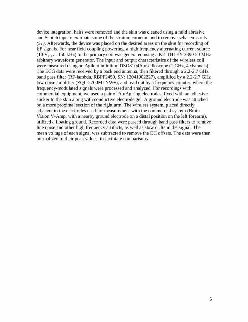
Fig. S23
Working principle of the multiplexer.

29
Fig. S24
The multifunctional sensor system with different parts and chip information (Table
S3) labeled. Black dots indicate the number 1 pin of each individual chip.

30
Fig. S25
Design strategy for reducing the power consumption of the voltage controlled
oscillator (VCO), by adding a pulse modulator. When the VCO duty cycle is reduced
to 7%, the power consumption of the entire system is about 6 mW.

31
Fig. S26
Releasable power supplies for the multifunctional system. (A) Optical image of the
NFC module from the front and back sides, and associated chip information (Table S1).
(B) Optical image of the front and back sides of a small coin cell battery module. Both of
these modules can laminate onto the power supply contact pads of the multifunctional
device, to provide power for operation.

32
Fig. S27
Images of the device on the skin. (A) Top down view to show its overall footprint (1.9 x
2.9 cm2), and (B) perspective view to show its overall thickness (~1 mm) with reference
to a coin (US quarter).

33
Fig. S28
Calibration curve for the temperature-frequency relationship in the multifunctional
system. The error bars for each data point are from three independent measurements.

34
Fig. S29
Signal readouts from the multifunctional device when mounted on the forearm
during periodic clinching and relaxing of the fist. (A) Acceleration signal and (B)
temperature signal before and after 9 min of clinching and relaxing. (C) The temperature
measured before (left panel) and after (right panel) this exercise, as confirmed by the
commercial IR camera.

35
Table S1
Chip information of the ECG system.

36
Table S2
Computational model for the effective Young’s modulus. The moduli for the
experimental data are determined by using linear fits of the stress-strain curve in the
range of [0%, 50%].

37
Table S3
Chip information for the multifunctional system.

38
Movie S1
Video of the self-alignment of chips during the soldering/bonding process. Under
controlled heating, the solder paste reflows and wets the serpentine metal electrodes and
the contact pads on the chips. The surface tension causes motion that maximizes the
contact area to the metal electrodes underneath, thereby self-aligning the chips.

39
Movie S2
This video shows an ECG device during operation. This device has three basic
functions: wireless power transfer, electrophysiological potential sensing and wireless
data transmission to an external receiving system. When the inductive coil is placed near
the secondary coil in the device, the ECG signal from the chest of a test subject was
amplified, filtered and wirelessly transmitted to a receiver. The resulting data appears in
real time on the computer screen, as it is recorded. The drifting baseline of the signal in
the first few seconds is because of a capacitor connected in series in the circuit.

1
References and Notes 1. D. H. Kim, N. Lu, R. Ma, Y. S. Kim, R. H. Kim, S. Wang, J. Wu, S. M. Won, H. Tao, A.
Islam, K. J. Yu, T. I. Kim, R. Chowdhury, M. Ying, L. Xu, M. Li, H. J. Chung, H. Keum, M. McCormick, P. Liu, Y. W. Zhang, F. G. Omenetto, Y. Huang, T. Coleman, J. A. Rogers, Epidermal electronics. Science 333, 838–843 (2011). doi:10.1126/science.1206157
2. J.-W. Jeong, W. H. Yeo, A. Akhtar, J. J. Norton, Y. J. Kwack, S. Li, S. Y. Jung, Y. Su, W. Lee, J. Xia, H. Cheng, Y. Huang, W. S. Choi, T. Bretl, J. A. Rogers, Materials and optimized designs for human-machine interfaces via epidermal electronics. Adv. Mater. 25, 6839–6846 (2013). doi:10.1002/adma.201301921 Medline
3. M. Kaltenbrunner, T. Sekitani, J. Reeder, T. Yokota, K. Kuribara, T. Tokuhara, M. Drack, R. Schwödiauer, I. Graz, S. Bauer-Gogonea, S. Bauer, T. Someya, An ultra-lightweight design for imperceptible plastic electronics. Nature 499, 458–463 (2013). doi:10.1038/nature12314 Medline
4. M. S. White, M. Kaltenbrunner, E. D. Głowacki, K. Gutnichenko, G. Kettlgruber, I. Graz, S. Aazou, C. Ulbricht, D. A. M. Egbe, M. C. Miron, Z. Major, M. C. Scharber, T. Sekitani, T. Someya, S. Bauer, N. S. Sariciftci, Ultrathin, highly flexible and stretchable PLEDs. Nat. Photonics 7, 811–816 (2013). doi:10.1038/nphoton.2013.188
5. M. S. Mannoor, H. Tao, J. D. Clayton, A. Sengupta, D. L. Kaplan, R. R. Naik, N. Verma, F. G. Omenetto, M. C. McAlpine, Graphene-based wireless bacteria detection on tooth enamel. Nat. Commun. 3, 763 (2012). doi:10.1038/ncomms1767 Medline
6. J. A. Rogers, M. G. Lagally, R. G. Nuzzo, Synthesis, assembly and applications of semiconductor nanomembranes. Nature 477, 45–53 (2011). doi:10.1038/nature10381 Medline
7. C. F. Pan, L. Dong, G. Zhu, S. Niu, R. Yu, Q. Yang, Y. Liu, Z. L. Wang, High-resolution electroluminescent imaging of pressure distribution using a piezoelectric nanowire LED array. Nat. Photonics 7, 752–758 (2013). doi:10.1038/nphoton.2013.191
8. C. Wang, D. Hwang, Z. Yu, K. Takei, J. Park, T. Chen, B. Ma, A. Javey, User-interactive electronic skin for instantaneous pressure visualization. Nat. Mater. 12, 899–904 (2013). doi:10.1038/nmat3711 Medline
9. S. C. B. Mannsfeld, B. C. Tee, R. M. Stoltenberg, C. V. Chen, S. Barman, B. V. Muir, A. N. Sokolov, C. Reese, Z. Bao, Highly sensitive flexible pressure sensors with microstructured rubber dielectric layers. Nat. Mater. 9, 859–864 (2010). doi:10.1038/nmat2834 Medline
10. D. J. Lipomi, M. Vosgueritchian, B. C. Tee, S. L. Hellstrom, J. A. Lee, C. H. Fox, Z. Bao, Skin-like pressure and strain sensors based on transparent elastic films of carbon nanotubes. Nat. Nanotechnol. 6, 788–792 (2011). doi:10.1038/nnano.2011.184 Medline
11. T. Sekitani, T. Someya, Stretchable organic integrated circuits for large-area electronic skin surfaces. MRS Bull. 37, 236–245 (2012). doi:10.1557/mrs.2012.42

2
12. G. Schwartz, B. C. Tee, J. Mei, A. L. Appleton, H. Kim, H. Wang, Z. Bao, Flexible polymer transistors with high pressure sensitivity for application in electronic skin and health monitoring. Nat. Commun. 4, 1859 (2013). doi:10.1038/ncomms2832 Medline
13. C. Keplinger, J. Y. Sun, C. C. Foo, P. Rothemund, G. M. Whitesides, Z. Suo, Stretchable, transparent, ionic conductors. Science 341, 984–987 (2013). doi:10.1126/science.1240228 Medline
14. M. Kubo, X. Li, C. Kim, M. Hashimoto, B. J. Wiley, D. Ham, G. M. Whitesides, Stretchable microfluidic radiofrequency antennas. Adv. Mater. 22, 2749–2752 (2010). doi:10.1002/adma.200904201 Medline
15. E. Palleau, S. Reece, S. C. Desai, M. E. Smith, M. D. Dickey, Self-healing stretchable wires for reconfigurable circuit wiring and 3D microfluidics. Adv. Mater. 25, 1589–1592 (2013). doi:10.1002/adma.201203921 Medline
16. D. M. Vogt, Y. L. Park, R. J. Wood, Design and Characterization of a Soft Multi-Axis Force Sensor Using Embedded Microfluidic Channels. IEEE Sens. J. 13, 4056–4064 (2013). doi:10.1109/JSEN.2013.2272320
17. S. Wagner, S. Bauer, Materials for stretchable electronics. MRS Bull. 37, 207–213 (2012). doi:10.1557/mrs.2012.37
18. T. Sterken, J. Vanfleteren, T. Torfs, M. O. de Beeck, F. Bossuyt, C. Van Hoof, Ultra-Thin Chip Package (UTCP) and stretchable circuit technologies for wearable ECG system. Conf. Proc. IEEE Eng. Med. Biol. Soc. 2011, 6886–6889 (2011). Medline
19. F. Axisa, D. Brosteaux, E. De Leersnyder, F. Bossuyt, J. Vanfleteren, B. Hermans, R. Puers, Conf. Proc. IEEE Eng. Med. Biol. Soc. 2011, 5687–5690 (2007). doi:10.1109/IEMBS.2007.4353637
20. M. Gonzalez, B. Vandevelde, W. Christiaens, Y.-Y. Hsu, F. Iker, F. Bossuyt, J. Vanfleteren, O. Sluis, P. H. M. Timmermans, Design and implementation of flexible and stretchable systems. Microelectron. Reliab. 51, 1069–1076 (2011). doi:10.1016/j.microrel.2011.03.012
21. H. Vandeparre, Q. Liu, I. R. Minev, Z. Suo, S. P. Lacour, Localization of folds and cracks in thin metal films coated on flexible elastomer foams. Adv. Mater. 25, 3117–3121 (2013). doi:10.1002/adma.201300587 Medline
22. A. Romeo, Q. H. Liu, Z. G. Suo, S. P. Lacour, Elastomeric substrates with embedded stiff platforms for stretchable electronics. Appl. Phys. Lett. 102, 131904 (2013). doi:10.1063/1.4799653
23. S. P. Lacour, S. Wagner, R. J. Narayan, T. Li, Z. G. Suo, Stiff subcircuit islands of diamondlike carbon for stretchable electronics. J. Appl. Phys. 100, 014913 (2006). doi:10.1063/1.2210170
24. Y. Lee, B. Giridhar, Z. Foo, D. Sylvester, D. B. Blaauw, A Sub-nW multi-stage temperature compensated timer for ultra-low-power sensor nodes. IEEE J. Solid-State Circuits 48, 2511–2521 (2013). doi:10.1109/JSSC.2013.2275660
25. Y. Lee, S. Bang, I. Lee, Y. Kim, G. Kim, M. H. Ghaed, P. Pannuto, P. Dutta, D. Sylvester, D. Blaauw, A modular 1 mm3 die-stacked sensing platform with low power I2C inter-die

3
communication and multi-modal energy harvesting. IEEE J. Solid-State Circuits 48, 229–243 (2013). doi:10.1109/JSSC.2012.2221233
26. Y. Sun, H. Luo, S. K. Das, A trust-based framework for fault-tolerant data aggregation in wireless multimedia sensor networks. IEEE Trans. Depend. Secure Comput. 9, 785–797 (2012). doi:10.1109/TDSC.2012.68
27. E. Y. Chow, M. M. Morris, P. P. Irazoqui, Implantable RF medical devices: The benefits of high-speed communication and much greater communication distances in biomedical applications. IEEE Microw. Mag. 14, 64–73 (2013). doi:10.1109/MMM.2013.2248586
28. S. Kim, J. S. Ho, A. S. Y. Poon, Midfield wireless powering of subwavelength autonomous devices. Phys. Rev. Lett. 110, 203905 (2013). doi:10.1103/PhysRevLett.110.203905
29. S. J. Thomas, R. R. Harrison, A. Leonardo, M. S. Reynolds, A battery-free multichannel digital neural/EMG telemetry system for flying insects. IEEE Trans. Biomed. Circuit Syst. 6, 424–436 (2012). doi:10.1109/TBCAS.2012.2222881
30. Y. Sun, W. M. Choi, H. Jiang, Y. Y. Huang, J. A. Rogers, Controlled buckling of semiconductor nanoribbons for stretchable electronics. Nat. Nanotechnol. 1, 201–207 (2006). doi:10.1038/nnano.2006.131 Medline
31. V. Medina, J. M. Clochesy, A. Omery, Comparison of electrode site preparation techniques. Heart Lung 18, 456–460 (1989). Medline


