
San Jose State University San Jose State University
SJSU ScholarWorks SJSU ScholarWorks
Master's Theses Master's Theses and Graduate Research
Summer 2019
Signal Integrity Optimization of RF/Microwave Transmission Lines Signal Integrity Optimization of RF/Microwave Transmission Lines
in Multilayer PCBs in Multilayer PCBs
Justin Thien Le San Jose State University
Follow this and additional works at: https://scholarworks.sjsu.edu/etd_theses
Recommended Citation Recommended Citation Le, Justin Thien, "Signal Integrity Optimization of RF/Microwave Transmission Lines in Multilayer PCBs" (2019). Master's Theses. 5036. DOI: https://doi.org/10.31979/etd.4ddq-zyef https://scholarworks.sjsu.edu/etd_theses/5036
This Thesis is brought to you for free and open access by the Master's Theses and Graduate Research at SJSU ScholarWorks. It has been accepted for inclusion in Master's Theses by an authorized administrator of SJSU ScholarWorks. For more information, please contact [email protected].
SIGNAL INTEGRITY OPTIMIZATION OF RF/MICROWAVE TRANSMISSION
LINES IN MULTILAYER PCBS
A Thesis
Presented to
The Faculty of the Department of Electrical Engineering
San José State University
In Partial Fulfillment
of the Requirements for the Degree
Master of Science
by
Justin T. Le
August 2019

© 2019
Justin T. Le
ALL RIGHTS RESERVED
The Designated Thesis Committee Approves the Thesis Titled
SIGNAL INTEGRITY OPTIMIZATION OF RF/MICROWAVE TRANSMISSION
LINES IN MULTILAYER PCBS
by
Justin T. Le
APPROVED FOR THE DEPARTMENT OF ELECTRICAL ENGINEERING
SAN JOSÉ STATE UNIVERSITY
August 2019
Lili He, Ph.D. Department of Electrical Engineering
Raymond S. Kwok, Ph.D. Department of Electrical Engineering
Hiu Yung Wong, Ph.D. Department of Electrical Engineering

ABSTRACT
SIGNAL INTEGRITY OPTIMIZATION OF RF/MICROWAVE TRANSMISSION
LINES IN MULTILAYER PCBS
by Justin T. Le
While allowing for flexible trace routing and device miniaturization, multilayer
printed circuit boards (PCB) suffer from performance issues at high frequency due to the
impedance mismatch caused by vertical transitions. In this paper, a process for
optimizing the high-speed performance of microstrip to stripline transitions in multilayer
PCBs is demonstrated. This includes strategic tuning of via dimensions using time-
domain reflectometry and an analysis of the use of shielding vias to prevent parasitic
cavity resonance. Simulations of optimized 2-layer, 4-layer, and 6-layer microstrip to
stripline transitions show a return loss of 20 dB up to 7 GHz. To demonstrate a useful
microwave application, a planar filter with a passband of 4 GHz to 6 GHz is submerged
6-layers. Simulation shows that when paired with the optimized vertical transitions, the
filter can maintain performance.

v
ACKNOWLEDGMENTS
First, thanks are due to my thesis committee chair, Dr. Lili He, for providing support
and for guiding me in my thesis work. In addition, I would like to thank Dr. Ray Kwok
for taking me under his wing, offering guidance on my thesis work, and allowing me to
be his apprentice at both school and work. I would also like to thank Dr. Hiu Yung Wong
for his contributions as a committee member. Furthermore, I would like to thank Vanessa
Barahona for bearing with me through my academic pursuit. Lastly, thanks are due to my
mom for always supporting me in my life journey.
vi
TABLE OF CONTENTS
List of Tables ………………………………………………………………………. viii
List of Figures ……………………………………………………………………… ix
List of Abbreviations ………………………………………………………………. xi
1 Introduction …………………………………………………………………….. 1
2 Theory ………………………………………………………………………….. 3
2.1 Telegrapher Equations …………………………………………………. 3
2.1.1 Transmission Lines and Characteristic Impedance ……………. . 7
2.1.2 Characteristic Impedance of a Coaxial Cable ………………….. 8
2.2 Impedance Mismatch and Reflection Coefficient ……………………… 8
2.3 Time-Domain Reflectometry …………………………………………… 10
2.4 S-parameters ……………………………………………………………. 11
3 Multilayer PCB Manufacturing Process ……………………………………….. 13
3.1 General Multilayer Manufacturing Process ……………………………. 13
3.2 High Frequency Considerations …….………………………………….. 14
3.2.1 Material Selection and PTFE …………………………………… 14
3.2.2 Bonding and Stack-Up …………………………………………. 15
3.2.3 Vertical Connections …………………………………………… 17
4 Literature Review ………………………………………………………………. 19
4.1 Lumped Element Model ………………………………………………... 19
4.2 EM Simulation Optimization ………………………………………….... 20
4.3 Shielding Vias and Coaxial Via ………………………………………… 21
4.4 Nonconventional Vias ………………………………………………….. 22
5 Design and Simulation …………………………………………………………. 24
5.1 PCB Stack-Up ………………………………………………………….. 24
5.2 Simulation Set-Up ……………………………………………………… 24
5.3 Via Stitching ………………….………………………………………… 25
5.4 Impedance Matching the Via …………………………………………... 32
5.4.1 Low Impedance Via ……………………………………………. 32
5.4.2 High Impedance Via …………………………………………… 33
5.4.3 Optimized Vias ………………………………………………… 35
5.5 Cascading a Planar Filter ………………………………………………. 37

vii
6 Conclusion ……………………………………………………………………… 42
6.1 Future Work …………………………………………………………….. 42
Literature Cited……………………………………………………………………… 44

viii
LIST OF TABLES
Table 1. PTFE Stack-Up Summary ……………………………………………… 16
Table 2. Common Bonding Materials ………………………. ………………….. 16
Table 3. Impedance Optimization Guidelines …………………………………… 20
Table 4. Guidelines for Other Parasitic Effects …………………………………. 21
Table 5. Via Stitch Spacing ……………………………………………………… 30
Table 6. Optimized Via Dimensions and Performance ………………………….. 36
Table 7. Filter Specifications ……………………………………………………. 39

ix
LIST OF FIGURES
Fig. 1. Lumped element model of a finite length transmission line …………… 5
Fig. 2. Various types of transmission lines ……………………………………. 7
Fig. 3. Transmission line with arbitrary load ZL ………………………………. 9
Fig. 4. Bounce diagram of a microstrip with and without a via ……………….. 11
Fig. 5. Two-port network and flow diagram …………………………………… 12
Fig. 6. PTFE stack-up options …………………………………………………. 15
Fig. 7. Via hole anatomy …..…………………………………………………… 18
Fig. 8. Lumped element model of a via ………………………………………… 19
Fig. 9. 3D model of 1-level transition with no stitching vias …..……………… 25
Fig. 10. S-parameters of 1-level transition with no stitching vias ………………. 26
Fig. 11. E-field plot of 1-level transition with no stitching vias ………….…….. 26
Fig. 12. 3D Model of 3-level transition with no stitching vias ..………………… 27
Fig. 13. S-parameters of 3-level transition with no stitching vias ……… ……… 27
Fig. 14. E-field plot of 3-level transition with no stitching vias ………………… 28
Fig. 15. 3D Model of 2, 4, 6, and 8 stitching vias ….…………………………… 29
Fig. 16. S-parameters of 0, 2, 4, 6, and 8 stitching vias ………………………… 30
x
Fig. 17. E-field plot before and after via stitching ………………………………. 31
Fig. 18. TDR of a low impedance via …………………………………………… 32
Fig. 19. S-parameters of low impedance via ……………………………………. 33
Fig. 20. TDR of a high impedance via ………………………………………….. 34
Fig. 21. S-parameters of high impedance via …………………………………… 34
Fig. 22. Optimized via for a 1, 2, and 3 level transition ………………………… 35
Fig. 23. Optimized via TDR …..………………………………………………… 35
Fig. 24. S-parameters of optimized 1, 2, and 3 level transitions ………………… 36
Fig. 25. S-parameters of 3-level transition ……………………………………… 37
Fig. 26. 3D models of cascaded 1, 2, and 3 level transitions …..……………….. 38
Fig. 27. S-parameters of cascaded 1, 2, and 3 level transitions ………………… 38
Fig. 28. 3D model of planar 3-pole filter …..…………………………………… 39
Fig. 29. S-parameters of planar 3-pole filter ……………………………………. 40
Fig. 30. 3D model of submerged 3-pole filter …………………………………… 40
Fig. 31. S-parameters of submerged 3-pole filter …..…………………………… 41
Fig. 32. S-parameters of submerged 3-pole filter after tuning …..……………… 41

xi
LIST OF ABBREVIATIONS
CTE Coefficient of Thermal Expansion
DC Direct Current
EM Electromagnetic
EMI Electromagnetic Interference
FEP Fluorinated Ethylene Propylene
FR-4 Fire Resistant Four
LCP Liquid Crystalline Polymer
PCB Printed Circuit Board
PTFE Polytetrafluoroethylene
RF Radio Frequency
TDR Time-Domain Reflectometry
VIA Vertical Interconnect Access

1
1 INTRODUCTION
With the ever-increasing demand for the miniaturization of electronics, multilayer
printed circuit boards (PCB) have been used to realize compact, high density devices.
While allowing for size reduction and flexibility in trace routing, the vertical transitions
from layer to layer can introduce signal integrity issues at high frequency. This includes
impedance mismatch, reflections, electromagnetic interference, bandwidth, mode
conversion, and insertion loss. Thus, multilayer PCBs are generally avoided by radio
frequency (RF) engineers and high-speed digital designers.
However, the crossover of traces is sometimes necessary and multilayer PCBs can
mitigate this issue. For RF designers, a crossover is needed in balanced power amplifiers
where the DC bias line is required to cross an RF signal line [1]. One solution has been to
use air-bridges or a coaxial cable to cross traces. This is nonideal because it is a
nonplanar structure and can increase size, cost, and complexity. In addition, crossovers
are also needed in beam-forming networks in which dense transmission line routings are
used [2].
In microwave applications, passive planar structures such as filters, couplers, and
power dividers can take up significant board space. The ability to bury these passive
structures in another layer can allow for a dramatic reduction in board size. Devices such
as a filter bank, which consists of multiple filters, must have each filter placed adjacent to
one another. The ability to vertically stack each filter could reduce the filter bank size to
the size of just one filter.

2
The vertical access interconnect, also known as via, is the vertical connection
between layers. Vias are most commonly realized as a copper plated, drilled hole and are
the primary reason multilayer PCB performance degrades at high frequencies. At low
frequencies, these vertical junctions do not present an issue. At high frequencies, any
discontinuities in geometry and material properties can cause signal reflections. Because
multilayer PCBs are restricted to only planar geometries and copper plated cylindrical
holes, it can be difficult to realize a seamless junction in which minimal reflection is
achieved. Thus, a planar design technique to optimize the electrical performance of the
via is needed.
In effort to mitigate this issue, the work in this thesis uses impedance matching
techniques and the concept of characteristic impedance to design an optimal via using
electromagnetic simulation. This includes an analysis of several design variations and a
general technique for ensuring optimal performance in multilayer PCBs.

3
2 THEORY
The issue of signal integrity is, in essence, a transmission line theory problem. While
it is typically unfamiliar to designers of low frequency circuits, RF engineers have been
using transmission line theory as early as World War II. The work in this thesis relies on
the core concepts, and it is important that the reader has some background. Thus, this
section discusses some of the foundational concepts. This includes the telegrapher
equations, characteristic impedance, reflection coefficient, and the S-parameters. In
addition, time-domain reflectometry is discussed.
2.1 Telegrapher Equations
The basis of modern electromagnetic theory was derived by James Clerk Maxwell in
a paper published in 1865 titled “A Dynamical Theory of Electromagnetic Field.” From
mathematical deduction, Maxwell theorized that light was a form of electromagnetic
wave. This theory was then experimentally validated by Hertz. Maxwell’s equations are
heavily based on the work of Gauss, Ampere, Faraday, and other physicists [3]. Prior to
his publication, electric field and magnetic field were considered separate entities, and
Maxwell’s work unified them to a single entity known as electromagnetic fields. The
original Maxwell’s equations were mathematically complex and difficult to understand.
Oliver Heaviside rewrote the original Maxwell’s equations into its modern, well-known
vector notation form which are shown below.
4
∇ × =−𝜕
𝜕𝑡− (1)
∇ × =𝜕
𝜕𝑡+ 𝐽 (2)
∇ ∙ = 𝜌 (3)
∇ ∙ = 0 (4)
While Maxwell’s equations provide a complete spatial description of electromagnetic
fields, they are often impractical to work with for engineering design purposes. Thus,
transmission line theory was developed as an extension of circuit theory to account for
electromagnetic wave propagation, and it is needed when the wavelength of a signal is
proportional to the physical size of the conductor. This is useful since electrical engineers
typically work with voltage and current instead of electric field and magnetic field. To
account for a propagating voltage or current wave, a finite length transmission line is
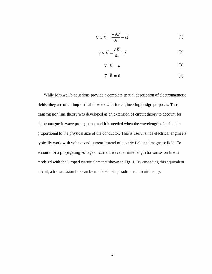
modeled with the lumped circuit elements shown in Fig. 1. By cascading this equivalent
circuit, a transmission line can be modeled using traditional circuit theory.
5
Fig. 1. Lumped element model of a finite length transmission line [3].
The series inductor represents the self-inductance of the two conductors, and the
shunt capacitor represents the capacitance between the two conductors. The series resistor
represents the loss due to the finite conductivity of the conductors, and the shunt resistor
represents the dielectric loss of the substrate material between the conductors since most
of the electromagnetic energy is in the substrate between the signal trace and ground.
This lumped element model yields the telegrapher equations which can be
mathematically manipulated to yield useful design parameters such as characteristic
impedance. Using Kirkoff’s voltage law on the lumped element model yields (5) and
Kirkoff’s current law yields (6). Rearranging the terms and taking the limit as ∆z → 0,
yields (7) and (8). Equations (7) and (8) are known as the telegrapher equations.

6
𝑣(𝑧, 𝑡) − 𝑅 ∆𝑧 𝑖(𝑧, 𝑡) − 𝐿 ∆𝑧 𝜕𝑖(𝑧, 𝑡)
𝜕𝑡− 𝑣(𝑧 + ∆𝑧 , 𝑡) = 0 (5)
𝑖(𝑧, 𝑡) − 𝐺 ∆𝑧 𝑣(𝑧 + ∆𝑧, 𝑡) − 𝐶 ∆𝑧 𝜕𝑣(𝑧 + ∆𝑧, 𝑡)
𝜕𝑡− 𝑖(𝑧 + ∆𝑧 , 𝑡) = 0 (6)
𝜕𝑣(𝑧, 𝑡)
𝜕𝑧= −𝑅𝑖(𝑧, 𝑡) − 𝐿
𝜕𝑖(𝑧, 𝑡)
𝜕𝑡 (7)
𝜕𝑖(𝑧, 𝑡)
𝜕𝑧= −𝐺𝑣(𝑧, 𝑡) − 𝐶
𝜕𝑣(𝑧, 𝑡)
𝜕𝑡 (8)
Assuming cosine-based phasors, (7) and (8) can be rewritten as (9) and (10) and
solving for V(z) and I(z) gives wave equations where γ is the complex propagation
constant. The traveling wave solutions can be written as (14) and (15). Finally, solving
for the characteristic impedance Zo yields (16).
𝑑𝑉(𝑧)
𝑑𝑧= −(𝑅 + 𝑗𝜔𝐿)𝐼(𝑧) (9)
𝑑𝐼(𝑧)
𝑑𝑧= −(𝐺 + 𝑗𝜔𝐶)𝑉(𝑧) (10)
𝑑2𝑉(𝑧)
𝑑𝑧2− 𝛾2𝑉(𝑧) = 0 (11)
𝑑2𝐼(𝑧)
𝑑𝑧2− 𝛾2𝐼(𝑧) = 0 (12)
𝛾 = 𝛼 + 𝑗𝛽 = √(𝑅 + 𝑗𝜔𝐿)(𝐺 + 𝑗𝜔𝐶) (13)
𝑉(𝑧) = 𝑉𝑜+𝑒−𝛾𝑧 + 𝑉𝑜
−𝑒𝛾𝑧 (14)
𝐼(𝑧) = 𝐼𝑜+𝑒−𝛾𝑧 + 𝐼𝑜
−𝑒𝛾𝑧 (15)
𝑍𝑜 =𝑅 + 𝑗𝜔𝐿
𝛾=
𝑉𝑜+
𝐼𝑜+ =
−𝑉𝑜−
𝐼𝑜−= √
𝑅 + 𝑗𝜔𝐿
𝐺 + 𝑗𝜔𝐶 (16)
7
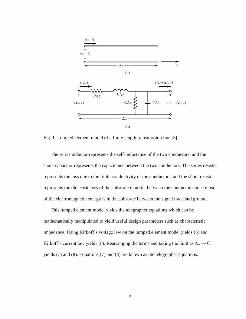
2.1.1 Transmission Lines and Characteristic Impedance
The primary metric of a transmission line is characteristic impedance. For a lossless
transmission line, the characteristic impedance can be simplified to be a real number as
shown in (17). This expression is widely used in microwave engineering for deriving the
characteristic impedance of many transmission line topologies. Fig. 2 shows several types
of transmission line. Common planar transmission lines used in multilayer PCBs include
microstrip, stripline, and coplanar waveguide. Standard characteristic impedances include
50 Ω, 75 Ω, and 100 Ω.
𝑅 = 𝐺 = 0
𝑍𝑜 = √𝐿
𝐶 (17)
𝑉 =1
√𝐿𝐶 (18)
(a) (b) (c)
(d) (e)
Fig. 2. Various types of transmission lines. (a) microstrip (b) stripline (c) coplanar
waveguide (d) coaxial (e) two wire.
8
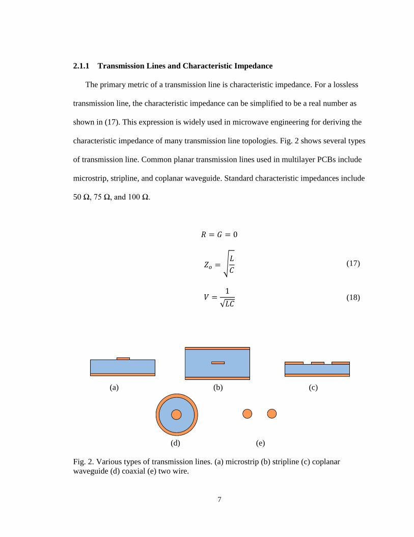
2.1.2 Characteristic Impedance of a Coaxial Cable
Due to radial symmetry, the characteristic impedance of a coaxial cable is
mathematically friendly to derive and is discussed for demonstration. The capacitance per
unit length (19) can be derived using Gauss’s law by using a cylinder as the Gaussian
surface. The inductance per unit length (20) can be derived using Ampere’s law and
using a circle as the Amperian loop. Substituting these equations into the characteristic
impedance equation yields (21).
𝐶 = 2𝜋𝜀𝑟𝜀𝑜
ln (𝑏𝑎)
(𝐹
𝑚) (19)
𝐿 =µ𝑜
2𝜋𝑙𝑛 (
𝑏
𝑎) (
𝐻
𝑚) (20)
𝑍𝑜 = √𝐿
𝐶=
√
µ𝑜
2𝜋 𝑙𝑛 (𝑏𝑎)
2𝜋𝜀𝑟𝜀𝑜
ln (𝑏𝑎)
= √µ𝑜
𝜀𝑟𝜀𝑜
𝑙𝑛 (𝑏𝑎)
2𝜋 (Ω) (21)
2.2 Impedance Mismatch and Reflection Coefficient
Transmission lines introduce the potential for reflected signals. The load of the
transmission line defines a boundary condition for the ratio of voltage to current that must
always be met. Since it takes a finite amount of time for the signal to propagate down the
line and reach the load, this boundary condition does not have an effect until the signal is
incident. Once the signal is incident on the load, a reflected wave must be propagated in
the opposite direction to satisfy the boundary condition. Fig. 3 shows a transmission line
with an arbitrary load. A reflection can occur at either end of the transmission line.
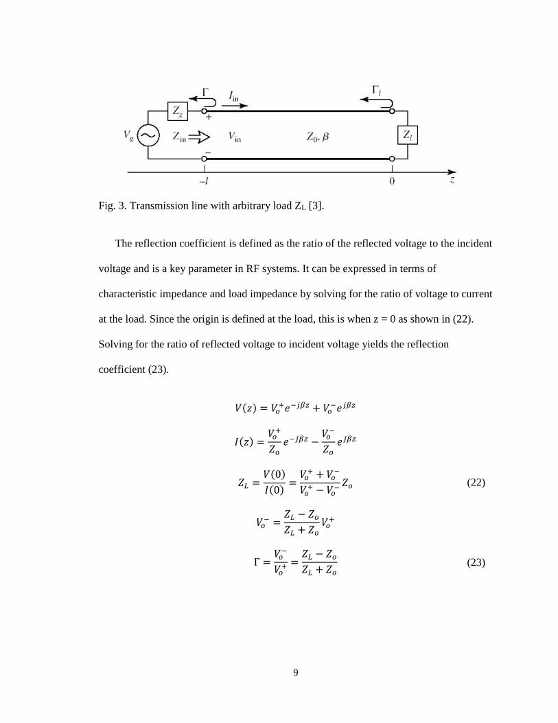
9
Fig. 3. Transmission line with arbitrary load ZL [3].
The reflection coefficient is defined as the ratio of the reflected voltage to the incident
voltage and is a key parameter in RF systems. It can be expressed in terms of
characteristic impedance and load impedance by solving for the ratio of voltage to current
at the load. Since the origin is defined at the load, this is when z = 0 as shown in (22).
Solving for the ratio of reflected voltage to incident voltage yields the reflection
coefficient (23).
𝑉(𝑧) = 𝑉𝑜+𝑒−𝑗𝛽𝑧 + 𝑉𝑜
−𝑒𝑗𝛽𝑧
𝐼(𝑧) =𝑉𝑜
+
𝑍𝑜𝑒−𝑗𝛽𝑧 −
𝑉𝑜−
𝑍𝑜𝑒𝑗𝛽𝑧
𝑍𝐿 =𝑉(0)
𝐼(0)=
𝑉𝑜+ + 𝑉𝑜
−
𝑉𝑜+ − 𝑉𝑜−
𝑍𝑜 (22)
𝑉𝑜− =
𝑍𝐿 − 𝑍𝑜
𝑍𝐿 + 𝑍𝑜𝑉𝑜
+
Γ =𝑉𝑜
−
𝑉𝑜+ =
𝑍𝐿 − 𝑍𝑜
𝑍𝐿 + 𝑍𝑜 (23)

10
From this equation, one can see that reflections occur when the impedance of a
transmission line does not match the impedance of the load. Thus, to achieve maximum
power transfer, it is required that the impedance of the generator and load match the
characteristic impedance of the transmission line. In a multilayer PCB, the via presents a
discontinuity in impedance and can cause reflections.
2.3 Time-Domain Reflectometry
A common tool for impedance matching is the smith chart, however, the smith chart
only describes the impedance looking into a port and does not describe the physical
location of where impedance mismatch occurs. To determine the physical location, one
can use time domain reflectometry (TDR) which utilizes a concept similar to radar. In
this technique, a step or an impulse is propagated through the network and the reflection
coefficient vs time is measured.
If the load impedance is higher than the characteristic impedance of the transmission
line, the reflected wave will have a positive amplitude, and constructively interfere with
the incident wave. Thus, the reflection coefficient will show an increase once the
reflected wave reaches the port. If the impedance is lower than the characteristic
impedance of the transmission line, the reflected wave will have a negative amplitude and
destructively interfere with the incident wave. This will show a decrease in reflection
coefficient once the reflected wave reaches the port. Based on the time delay and the
speed of propagation, one can determine the location at which a reflection is induced and
whether the junction is higher or lower in impedance.
11
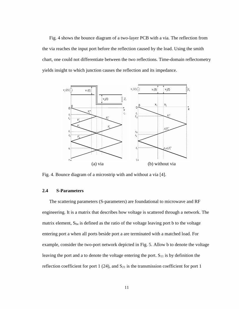
Fig. 4 shows the bounce diagram of a two-layer PCB with a via. The reflection from
the via reaches the input port before the reflection caused by the load. Using the smith
chart, one could not differentiate between the two reflections. Time-domain reflectometry
yields insight to which junction causes the reflection and its impedance.
(a) via (b) without via
Fig. 4. Bounce diagram of a microstrip with and without a via [4].
2.4 S-Parameters
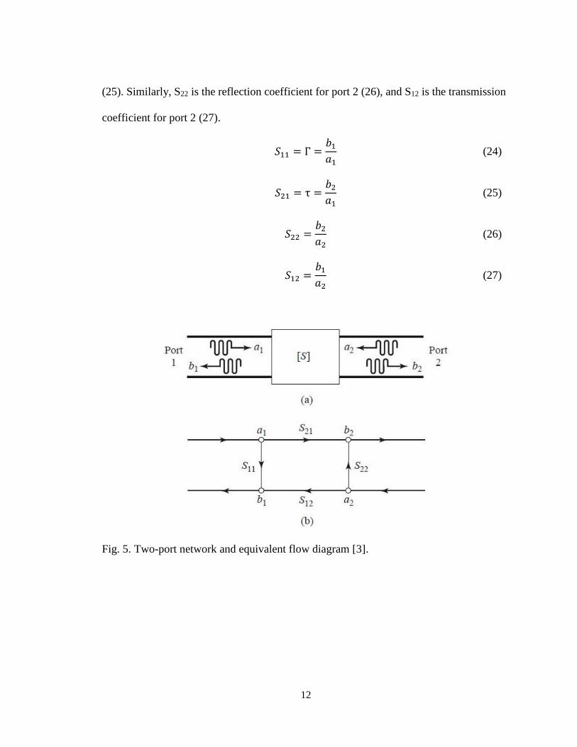
The scattering parameters (S-parameters) are foundational to microwave and RF
engineering. It is a matrix that describes how voltage is scattered through a network. The
matrix element, Sba is defined as the ratio of the voltage leaving port b to the voltage
entering port a when all ports beside port a are terminated with a matched load. For
example, consider the two-port network depicted in Fig. 5. Allow b to denote the voltage
leaving the port and a to denote the voltage entering the port. S11 is by definition the
reflection coefficient for port 1 (24), and S21 is the transmission coefficient for port 1
12
(25). Similarly, S22 is the reflection coefficient for port 2 (26), and S12 is the transmission
coefficient for port 2 (27).
𝑆11 = Γ =𝑏1
𝑎1 (24)
𝑆21 = τ =𝑏2
𝑎1 (25)
𝑆22 =𝑏2
𝑎2 (26)
𝑆12 =𝑏1
𝑎2 (27)
Fig. 5. Two-port network and equivalent flow diagram [3].

13
3 MULTILAYER PCB MANUFACTURING PROCESS
Prior to starting a design, it is important to understand the limitations presented by the
manufacturing process. The fabrication of a multilayer PCB is quite involved, and the
general process is described below [5].
3.1 General Multilayer PCB Manufacturing Process
The process starts with the innermost layer. The design is first printed on a
transparent film that is used for photo-etching the copper clad. The copper clad laminate
is then uniformly coated with a light sensitive film called the photoresist. Since each
layer of the PCB needs to line up, precise alignment holes are punched into the films and
laminates. The copper clad laminate is aligned with the film containing the design and is
then exposed to intense UV light which hardens the photoresist. The areas that are
covered by the hardened photoresist are where the copper will be. The exposed copper
that is not covered by the hardened photoresist will be dissolved away using an alkaline
solution. Once the unwanted copper is dissolved, the hardened photoresist is removed
using a chemical solution and the innermost layer is ready to be bonded to its surrounding
layers.
To adhere two layers together, a laminate impregnated with uncured epoxy resin
called prepeg is used. The layers and prepeg are tightly sandwiched in a press and heated
in an oven to cure the epoxy resin. This bonds the layers together. An X-ray drill is then
used to drills vias precisely at the center of the via pads. The via holes are then plated
with copper using electroplating. The photoetching, layer bonding, drilling, and plating
process is repeated for each layer until the board is complete [5].
14
3.2 High Frequency Considerations
Due to transmission line effects, additional considerations must be made to maintain
performance at high frequency. This includes material selection, layer bonding technique,
and via dimensions.
3.2.1 Material Selection and PTFE
The primary distinction is the choice of substrate materials. In a transmission line, the
signal propagates as an electromagnetic wave between the signal trace and the ground
plane. Thus, the material properties of the substrate heavily define the characteristics of
the transmission line. Key parameters include dielectric constant and loss tangent.
Conventional materials used in low frequency applications such as FR-4 are
mechanically rigid and inexpensive but are lossy at high frequency. Therefore, special
substrate materials such as polytetrafluroethylene (PTFE) are preferred for RF
application.
PTFE is widely used in microwave circuits for its low dielectric constant and low
loss. However, PTFE has several drawbacks that can make it difficult to use in a
multilayer PCB.
PTFE laminates have a relatively high coefficient of thermal expansion (CTE).
Manufacturers offer laminates which are structurally reinforced with fiberglass, glass
fiber, or ceramic fillers. This helps with the thermal expansion along the plane of the
laminate, but the thickness of the laminate can still increase with temperature. This can be
problematic for plated through holes, as they can fatigue and crack after many
temperature cycles [6].
15
PTFE laminates are also relatively expensive. Therefore, it is sometimes desirable to
mix PTFE with less expensive materials. Hybrid multilayer PCBs made from both PTFE
and FR-4 are ideal for boards that contain both DC and RF signals. It is important to
choose materials with a similar CTE to prevent mechanical issues such as delamination.
To prevent delamination and cracking of plated through holes, one should choose
laminates with a CTE closest to that of copper.
In addition, PTFE is a relatively soft material which requires special drilling and
plating techniques for the vias, thus a PCB manufacturer who specializes with PTFE
should be used [7].
3.2.2 Bonding and Stack-Up
The stack-up is the order in which the laminates are bonded together. For low
frequency applications, a prepeg layer is used for bonding. For high frequency
applications, this prepeg presents a discontinuity in the material properties and must be
considered in the electrical design as it can change the characteristic impedance of a
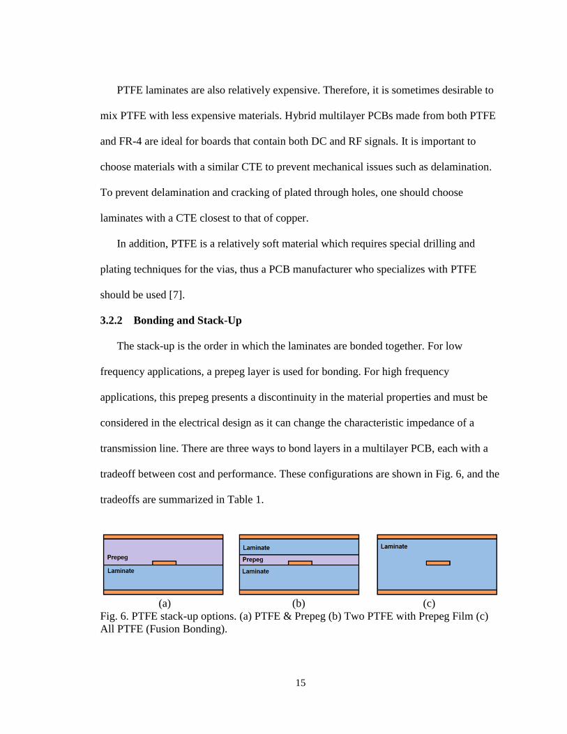
transmission line. There are three ways to bond layers in a multilayer PCB, each with a
tradeoff between cost and performance. These configurations are shown in Fig. 6, and the
tradeoffs are summarized in Table 1.
(a) (b) (c)
Fig. 6. PTFE stack-up options. (a) PTFE & Prepeg (b) Two PTFE with Prepeg Film (c)
All PTFE (Fusion Bonding).
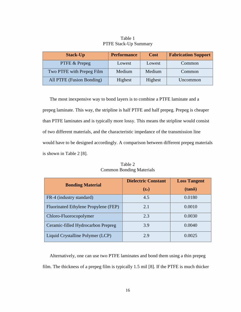
16
Table 1
PTFE Stack-Up Summary
Stack-Up Performance Cost Fabrication Support
PTFE & Prepeg Lowest Lowest Common
Two PTFE with Prepeg Film Medium Medium Common
All PTFE (Fusion Bonding) Highest Highest Uncommon
The most inexpensive way to bond layers is to combine a PTFE laminate and a
prepeg laminate. This way, the stripline is half PTFE and half prepeg. Prepeg is cheaper
than PTFE laminates and is typically more lossy. This means the stripline would consist
of two different materials, and the characteristic impedance of the transmission line
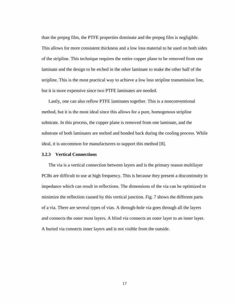
would have to be designed accordingly. A comparison between different prepeg materials
is shown in Table 2 [8].
Table 2
Common Bonding Materials
Bonding Material Dielectric Constant
(εr)
Loss Tangent
(tanδ)
FR-4 (industry standard) 4.5 0.0180
Fluorinated Ethylene Propylene (FEP) 2.1 0.0010
Chloro-Fluorocopolymer 2.3 0.0030
Ceramic-filled Hydrocarbon Prepreg 3.9 0.0040
Liquid Crystalline Polymer (LCP) 2.9 0.0025
Alternatively, one can use two PTFE laminates and bond them using a thin prepeg
film. The thickness of a prepeg film is typically 1.5 mil [8]. If the PTFE is much thicker
17
than the prepeg film, the PTFE properties dominate and the prepeg film is negligible.
This allows for more consistent thickness and a low loss material to be used on both sides
of the stripline. This technique requires the entire copper plane to be removed from one
laminate and the design to be etched in the other laminate to make the other half of the
stripline. This is the most practical way to achieve a low loss stripline transmission line,
but it is more expensive since two PTFE laminates are needed.
Lastly, one can also reflow PTFE laminates together. This is a nonconventional
method, but it is the most ideal since this allows for a pure, homogenous stripline
substrate. In this process, the copper plane is removed from one laminate, and the
substrate of both laminates are melted and bonded back during the cooling process. While
ideal, it is uncommon for manufacturers to support this method [8].
3.2.3 Vertical Connections
The via is a vertical connection between layers and is the primary reason multilayer
PCBs are difficult to use at high frequency. This is because they present a discontinuity in
impedance which can result in reflections. The dimensions of the via can be optimized to
minimize the reflection caused by this vertical junction. Fig. 7 shows the different parts
of a via. There are several types of vias. A through-hole via goes through all the layers
and connects the outer most layers. A blind via connects an outer layer to an inner layer.
A buried via connects inner layers and is not visible from the outside.
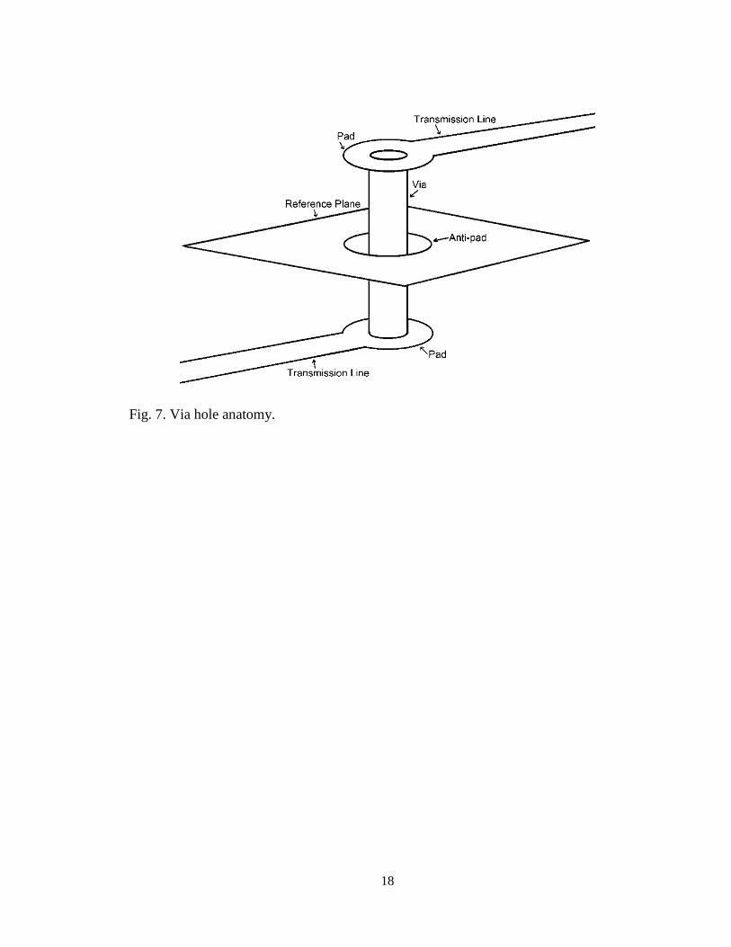
18
Fig. 7. Via hole anatomy.
19
4 LITERATURE REVIEW
4.1 Lumped Element Model
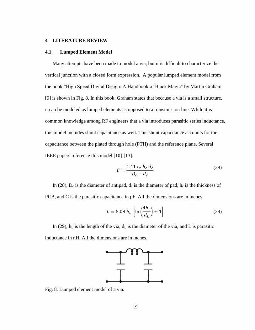
Many attempts have been made to model a via, but it is difficult to characterize the
vertical junction with a closed form expression. A popular lumped element model from
the book “High Speed Digital Design: A Handbook of Black Magic” by Martin Graham
[9] is shown in Fig. 8. In this book, Graham states that because a via is a small structure,
it can be modeled as lumped elements as opposed to a transmission line. While it is
common knowledge among RF engineers that a via introduces parasitic series inductance,
this model includes shunt capacitance as well. This shunt capacitance accounts for the
capacitance between the plated through hole (PTH) and the reference plane. Several
IEEE papers reference this model [10]-[13].
𝐶 =
1.41 𝜀𝑟 ℎ𝑐 𝑑𝑐
𝐷𝑐 − 𝑑𝑐
(28)
In (28), Dc is the diameter of antipad, dc is the diameter of pad, hc is the thickness of
PCB, and C is the parasitic capacitance in pF. All the dimensions are in inches.
𝐿 = 5.08 ℎ𝐿 [ln (4ℎ𝐿
𝑑𝐿) + 1]
(29)
In (29), hL is the length of the via, dL is the diameter of the via, and L is parasitic
inductance in nH. All the dimensions are in inches.
Fig. 8. Lumped element model of a via.
20
4.2 EM Simulation Optimization
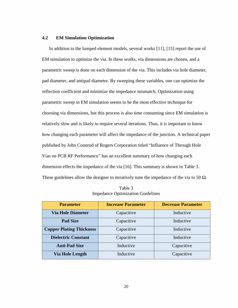
In addition to the lumped element models, several works [11], [15] report the use of
EM simulation to optimize the via. In these works, via dimensions are chosen, and a
parametric sweep is done on each dimension of the via. This includes via hole diameter,
pad diameter, and antipad diameter. By sweeping these variables, one can optimize the
reflection coefficient and minimize the impedance mismatch. Optimization using
parametric sweep in EM simulation seems to be the most effective technique for
choosing via dimensions, but this process is also time consuming since EM simulation is
relatively slow and is likely to require several iterations. Thus, it is important to know
how changing each parameter will affect the impedance of the junction. A technical paper
published by John Coonrod of Rogers Corporation titled “Influence of Through Hole
Vias on PCB RF Performance” has an excellent summary of how changing each
dimension effects the impedance of the via [16]. This summary is shown in Table 3.
These guidelines allow the designer to iteratively tune the impedance of the via to 50 Ω.
Table 3
Impedance Optimization Guidelines
Parameter Increase Parameter Decrease Parameter
Via Hole Diameter Capacitive Inductive
Pad Size Capacitive Inductive
Copper Plating Thickness Capacitive Inductive
Dielectric Constant Capacitive Inductive
Anti-Pad Size Inductive Capacitive
Via Hole Length Inductive Capacitive
21
One IEEE paper [13] mentions that a buried via has more shunt capacitance due to
there being a reference plane on both sides of the via. This means a through hole, blind,
and buried via would need to have slightly different geometries to achieve minimal
reflection. It was also suggested that if less capacitance was needed, a hole in either
reference plane could be made to reduce shunt capacitance.
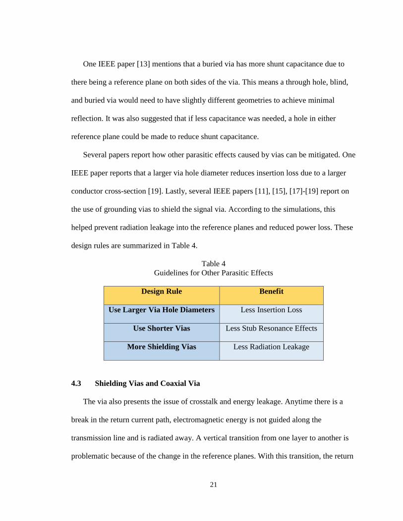
Several papers report how other parasitic effects caused by vias can be mitigated. One
IEEE paper reports that a larger via hole diameter reduces insertion loss due to a larger
conductor cross-section [19]. Lastly, several IEEE papers [11], [15], [17]-[19] report on
the use of grounding vias to shield the signal via. According to the simulations, this
helped prevent radiation leakage into the reference planes and reduced power loss. These
design rules are summarized in Table 4.
Table 4
Guidelines for Other Parasitic Effects
Design Rule Benefit
Use Larger Via Hole Diameters Less Insertion Loss
Use Shorter Vias Less Stub Resonance Effects
More Shielding Vias Less Radiation Leakage
4.3 Shielding Vias and Coaxial Via
The via also presents the issue of crosstalk and energy leakage. Anytime there is a
break in the return current path, electromagnetic energy is not guided along the
transmission line and is radiated away. A vertical transition from one layer to another is
problematic because of the change in the reference planes. With this transition, the return
22
current path is not clear and electromagnetic energy can leak between the reference
planes.
Several IEEE papers [11], [15], [17]-[19] study the effect of shielding vias. Shielding
vias surround the signal via and connect the reference planes of each layer. This creates a
path for return current and helps guide the electromagnetic energy. Without shielding
vias, electromagnetic energy is able to radiate and excite modes between the reference
planes. EM simulation shows that without the vias, the insertion loss has a sharp roll-off
at the first resonant frequency from mode excitation between reference planes. This can
also result in cross talk with nearby transmission lines. With 8 shielding vias, the resonant
frequency is removed, and the insertion loss is minimal [15]. A simulated E-field
magnitude plot also showed that the electromagnetic field is well contained in the
shielding vias.
One paper reports on a technique that can be used to measure the capacitance of the
via and suggested that if the number of reference planes is increased, the vertical
transition can resemble a coaxial cable. The measured capacitance was close to the
calculated value for a coaxial cable [12].
4.4 Nonconventional Vias
Outside of the traditional via, several experiments on nonconventional vias have been
reported. One IEEE paper [20] tested several different shapes of via hole pad. Instead of a
simple circle, shapes such as a bottleneck, taper, and no taper were tested. After the
designs were optimized in EM software, measurements showed that each shape yielded

23
3 dB to 5 dB improvement in return loss when compared to a traditional via. However,
measurements were only shown up to 3 GHz.
Another paper [21] tested a row of vias to connect two microstrips. The design was
optimized using HFSS, and the simulation matched measurements up to 8 GHz.
Measurements showed a return loss of at least -20 dB up to 8 GHz, and an insertion loss
of less than -1 dB up to 8 GHz.
Lastly, two unique papers [22], [23] used 3D printing to construct a via. This allowed
for nonplanar geometries to be tested. One paper tested a tapered ramp for a microstrip to
stripline transition. Both 3D printed vias had limited performance.

24
5 DESIGN AND SIMULATION
Since many combinations of planar transmission lines, substrate materials, and
substrate thicknesses are possible, the work in this thesis is aimed to demonstrate a
general process for maintaining high frequency performance in multilayer PCBs for any
application. The transmission lines for these simulations are microstrip and stripline, and
simulations of a 1-level, 2-level, and 3-level transition are shown.
5.1 PCB Stack-Up
The dimensions of the simulated PCB are chosen to be realistic for manufacturing.
The substrate used is Rogers Duroid 6006 which has a dielectric constant of 6.15 and a
loss tangent of 0.0018. A 3-level drop requires 7 laminates. Thicker substrates are
preferred by PCB fabricators when more layers are used. The layer thicknesses used
include 20 mil for the uppermost layer and 30 mil for the other layers. This allows for a
50 Ω microstrip to have a width of 30 mils and a 50 Ω stripline to have a width of 18
mils. Lastly, an air cavity height of 140 mils is chosen.
5.2 Simulation Set-Up
For EM simulations, Ansys HFSS 15.0 was used. Wave ports were used to excite the
microstrip and stripline, and the recommended port sizing as published by Ansys was
used. Port widths of 8 times the transmission line widths are chosen for both ports. The
conductors are modeled as zero thickness, 2D planar structures. The boundary chosen is
perfect E-field. The substrate is defined as Rogers Duroid 6006 from the HFSS material
library and fusion bonding is assumed for layer bonding.
25
5.3 Via Stitching
In a multilayer PCB, it is necessary to connect the reference planes near the signal
via, otherwise the space between each reference plane forms a cavity that can be excited
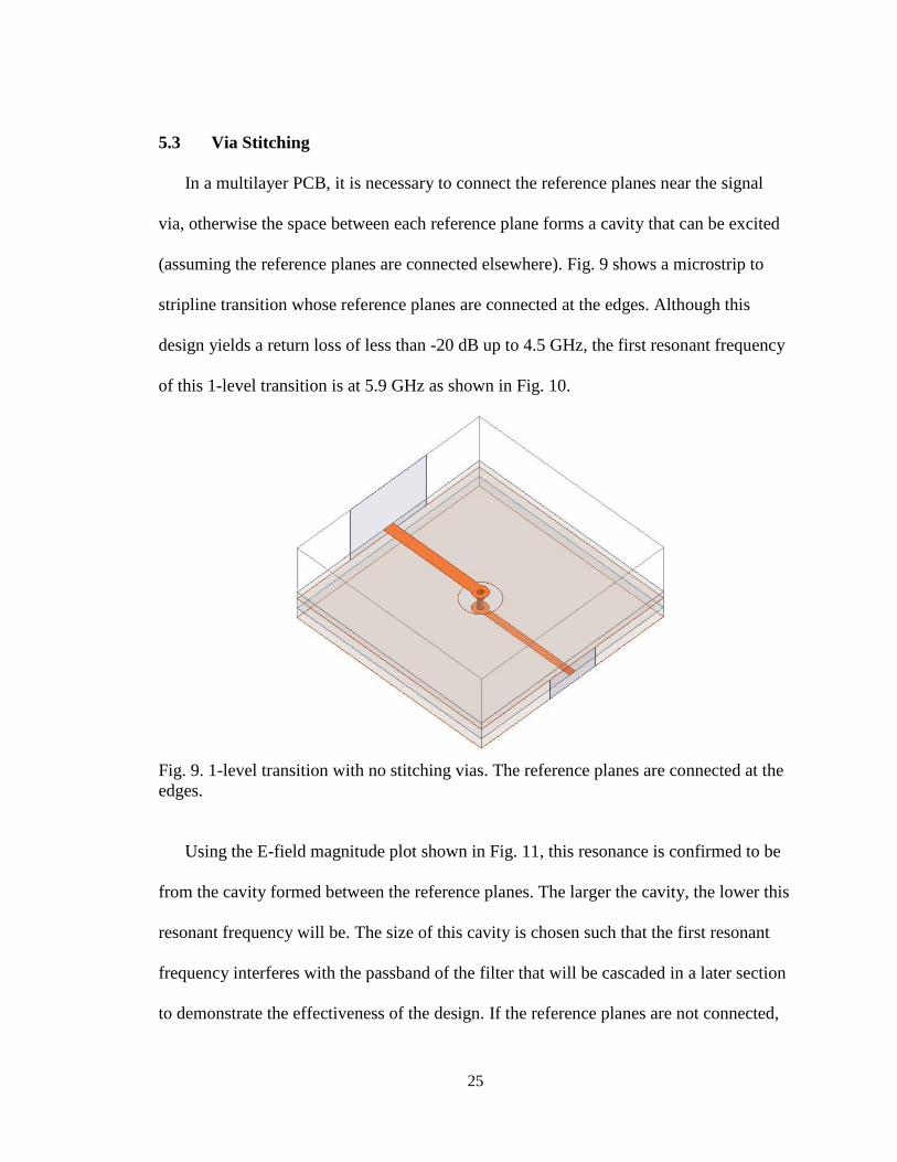
(assuming the reference planes are connected elsewhere). Fig. 9 shows a microstrip to
stripline transition whose reference planes are connected at the edges. Although this
design yields a return loss of less than -20 dB up to 4.5 GHz, the first resonant frequency
of this 1-level transition is at 5.9 GHz as shown in Fig. 10.
Fig. 9. 1-level transition with no stitching vias. The reference planes are connected at the
edges.
Using the E-field magnitude plot shown in Fig. 11, this resonance is confirmed to be
from the cavity formed between the reference planes. The larger the cavity, the lower this
resonant frequency will be. The size of this cavity is chosen such that the first resonant
frequency interferes with the passband of the filter that will be cascaded in a later section
to demonstrate the effectiveness of the design. If the reference planes are not connected,

26
there will be no cavity resonance effect, but the signal will be radiated away resulting in
significant insertion loss.
Fig. 10. S-parameters of the 1-level transition with no stitching vias.
Fig. 11. E-field magnitude plot at 5.9 GHz. Without stitching vias, modes can be excited
between the reference planes.
27
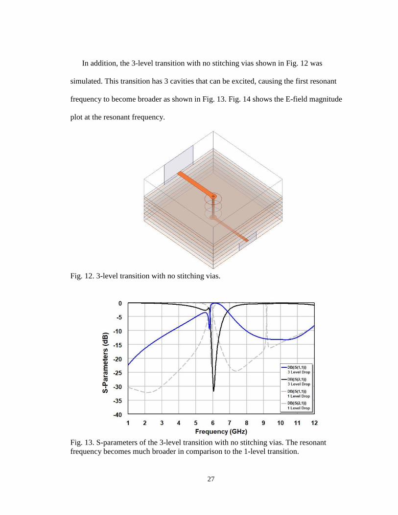
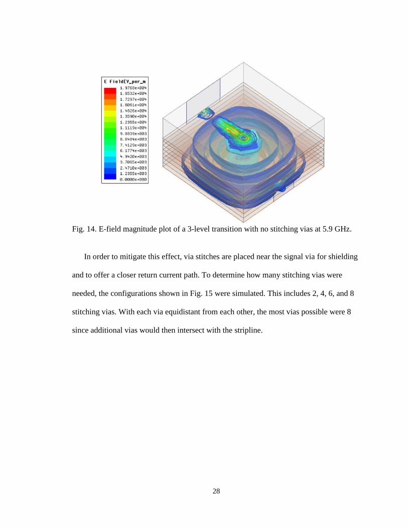
In addition, the 3-level transition with no stitching vias shown in Fig. 12 was
simulated. This transition has 3 cavities that can be excited, causing the first resonant
frequency to become broader as shown in Fig. 13. Fig. 14 shows the E-field magnitude
plot at the resonant frequency.
Fig. 12. 3-level transition with no stitching vias.
Fig. 13. S-parameters of the 3-level transition with no stitching vias. The resonant
frequency becomes much broader in comparison to the 1-level transition.
28
Fig. 14. E-field magnitude plot of a 3-level transition with no stitching vias at 5.9 GHz.
In order to mitigate this effect, via stitches are placed near the signal via for shielding
and to offer a closer return current path. To determine how many stitching vias were
needed, the configurations shown in Fig. 15 were simulated. This includes 2, 4, 6, and 8
stitching vias. With each via equidistant from each other, the most vias possible were 8
since additional vias would then intersect with the stripline.

29
Fig. 15. 2, 4, 6, and 8 stitching vias on a 3-level transition.
30
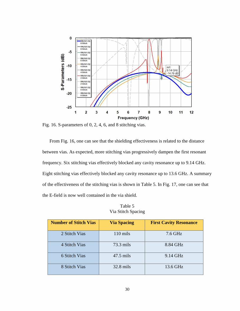
Fig. 16. S-parameters of 0, 2, 4, 6, and 8 stitching vias.
From Fig. 16, one can see that the shielding effectiveness is related to the distance
between vias. As expected, more stitching vias progressively dampen the first resonant
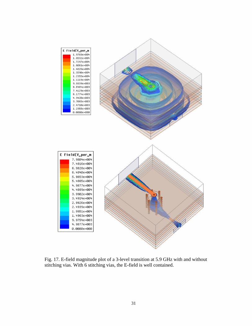
frequency. Six stitching vias effectively blocked any cavity resonance up to 9.14 GHz.
Eight stitching vias effectively blocked any cavity resonance up to 13.6 GHz. A summary
of the effectiveness of the stitching vias is shown in Table 5. In Fig. 17, one can see that
the E-field is now well contained in the via shield.
Table 5
Via Stitch Spacing
Number of Stitch Vias Via Spacing First Cavity Resonance
2 Stitch Vias 110 mils 7.6 GHz
4 Stitch Vias 73.3 mils 8.84 GHz
6 Stitch Vias 47.5 mils 9.14 GHz
8 Stitch Vias 32.8 mils 13.6 GHz
31
Fig. 17. E-field magnitude plot of a 3-level transition at 5.9 GHz with and without
stitching vias. With 6 stitching vias, the E-field is well contained.
32
5.4 Impedance Matching the Via
In addition to via stitching, it is critical to choose dimensions such that the impedance
of the via matches that of the transmission lines. To do this, time-domain reflectometry in
HFSS is used, and the guidelines in Table 3 are followed. Since the substrate thickness
and dielectric constant are fixed, there are only four parameters that can be tuned to
control the impedance. This includes via radius, microstrip pad radius, stripline pad
radius, and antipad radius. Arbitrarily choosing these dimensions can result in a low
impedance via or a high impedance via and the tuning process for both are shown.
5.4.1 Low Impedance Via
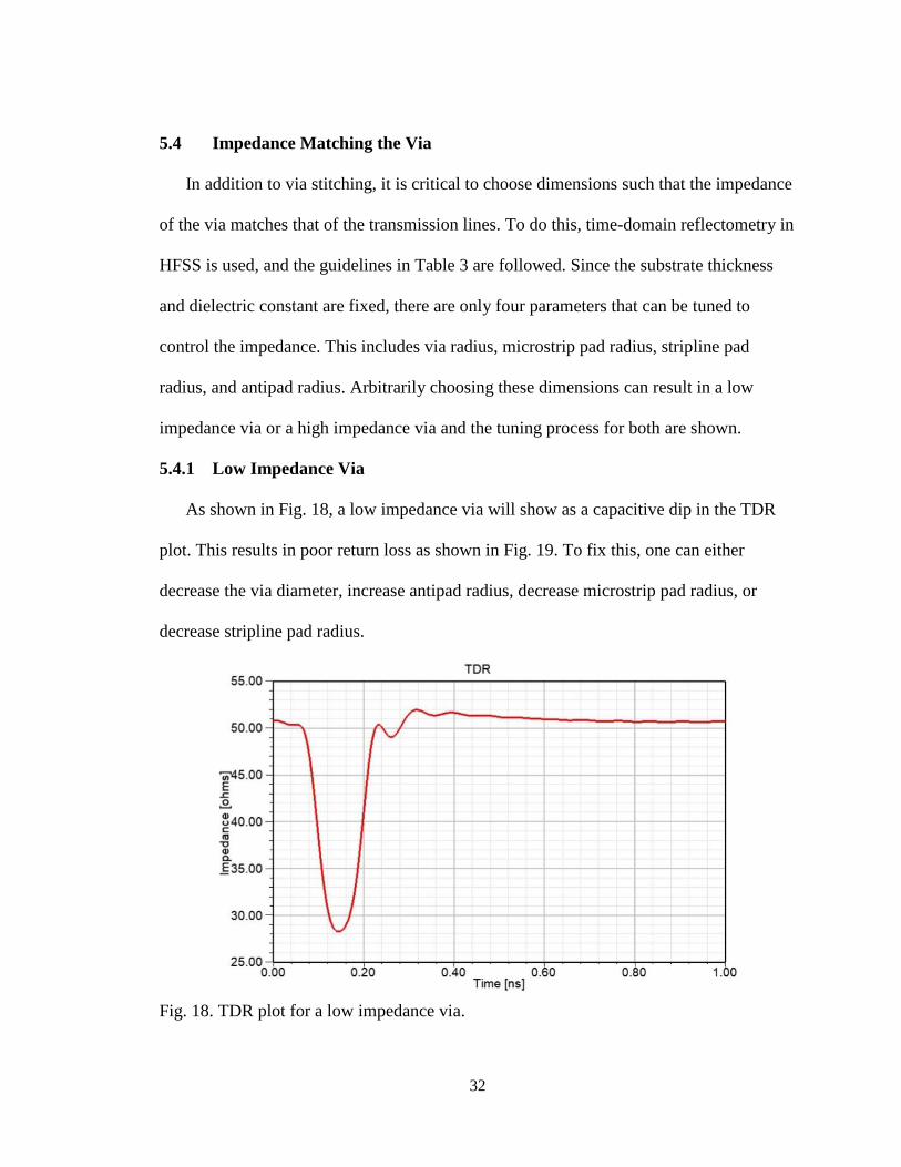
As shown in Fig. 18, a low impedance via will show as a capacitive dip in the TDR
plot. This results in poor return loss as shown in Fig. 19. To fix this, one can either
decrease the via diameter, increase antipad radius, decrease microstrip pad radius, or
decrease stripline pad radius.
Fig. 18. TDR plot for a low impedance via.
33
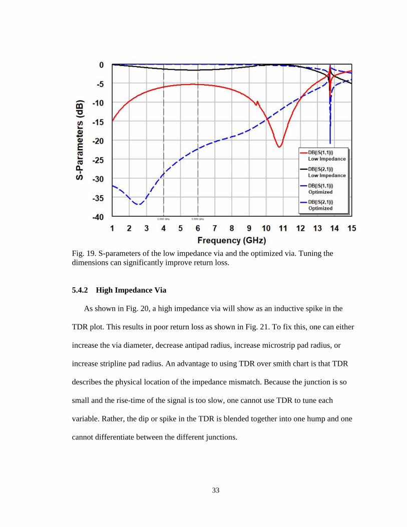
Fig. 19. S-parameters of the low impedance via and the optimized via. Tuning the
dimensions can significantly improve return loss.
5.4.2 High Impedance Via
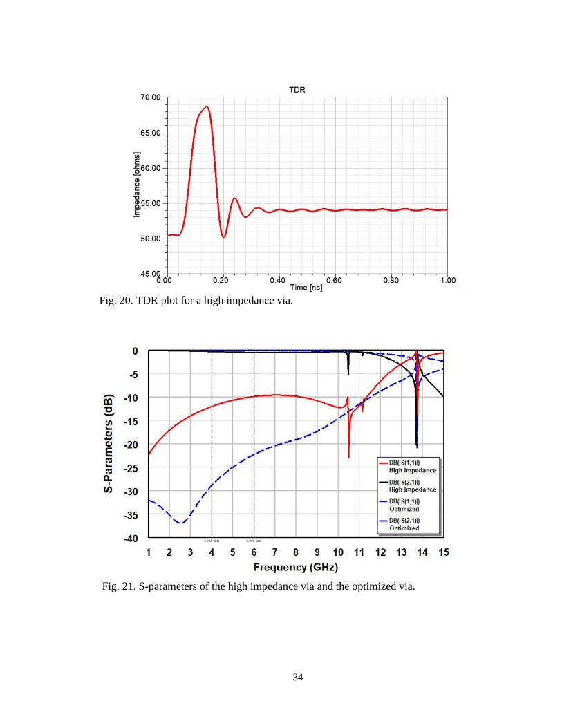
As shown in Fig. 20, a high impedance via will show as an inductive spike in the
TDR plot. This results in poor return loss as shown in Fig. 21. To fix this, one can either
increase the via diameter, decrease antipad radius, increase microstrip pad radius, or
increase stripline pad radius. An advantage to using TDR over smith chart is that TDR
describes the physical location of the impedance mismatch. Because the junction is so
small and the rise-time of the signal is too slow, one cannot use TDR to tune each
variable. Rather, the dip or spike in the TDR is blended together into one hump and one
cannot differentiate between the different junctions.
34
Fig. 20. TDR plot for a high impedance via.
Fig. 21. S-parameters of the high impedance via and the optimized via.
35
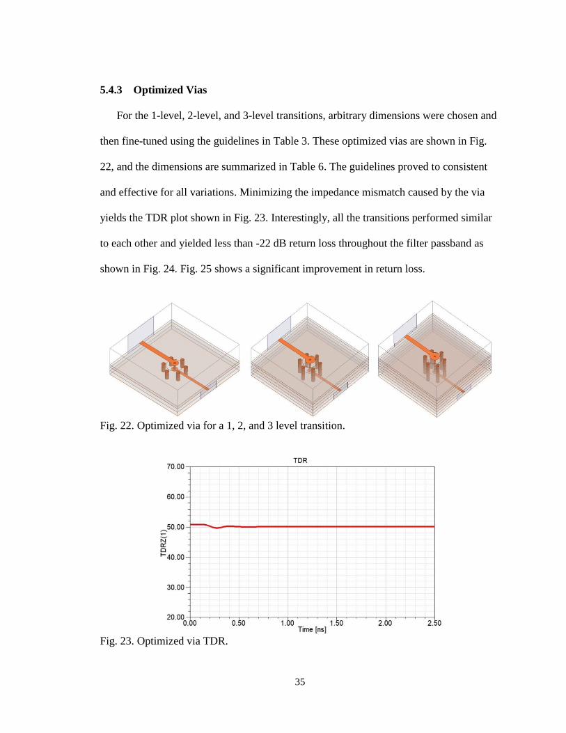
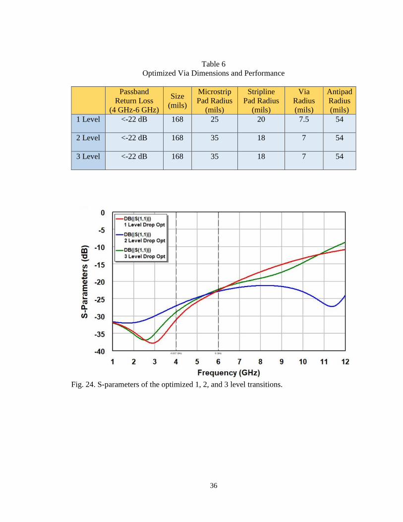
5.4.3 Optimized Vias
For the 1-level, 2-level, and 3-level transitions, arbitrary dimensions were chosen and
then fine-tuned using the guidelines in Table 3. These optimized vias are shown in Fig.
22, and the dimensions are summarized in Table 6. The guidelines proved to consistent
and effective for all variations. Minimizing the impedance mismatch caused by the via
yields the TDR plot shown in Fig. 23. Interestingly, all the transitions performed similar
to each other and yielded less than -22 dB return loss throughout the filter passband as
shown in Fig. 24. Fig. 25 shows a significant improvement in return loss.
Fig. 22. Optimized via for a 1, 2, and 3 level transition.
Fig. 23. Optimized via TDR.
36
Table 6
Optimized Via Dimensions and Performance
Passband
Return Loss
(4 GHz-6 GHz)
Size
(mils)
Microstrip
Pad Radius
(mils)
Stripline
Pad Radius
(mils)
Via
Radius
(mils)
Antipad
Radius
(mils)
1 Level <-22 dB 168 25 20 7.5 54
2 Level <-22 dB 168 35 18 7 54
3 Level <-22 dB 168 35 18 7 54
Fig. 24. S-parameters of the optimized 1, 2, and 3 level transitions.
37
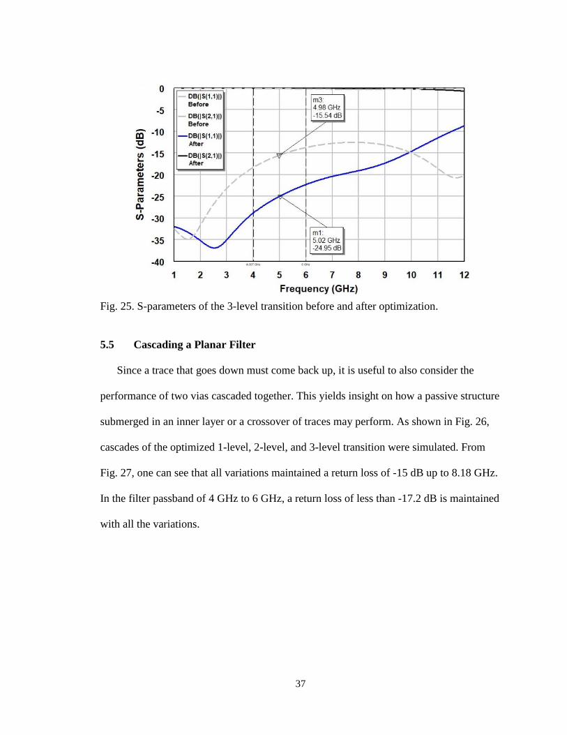
Fig. 25. S-parameters of the 3-level transition before and after optimization.
5.5 Cascading a Planar Filter
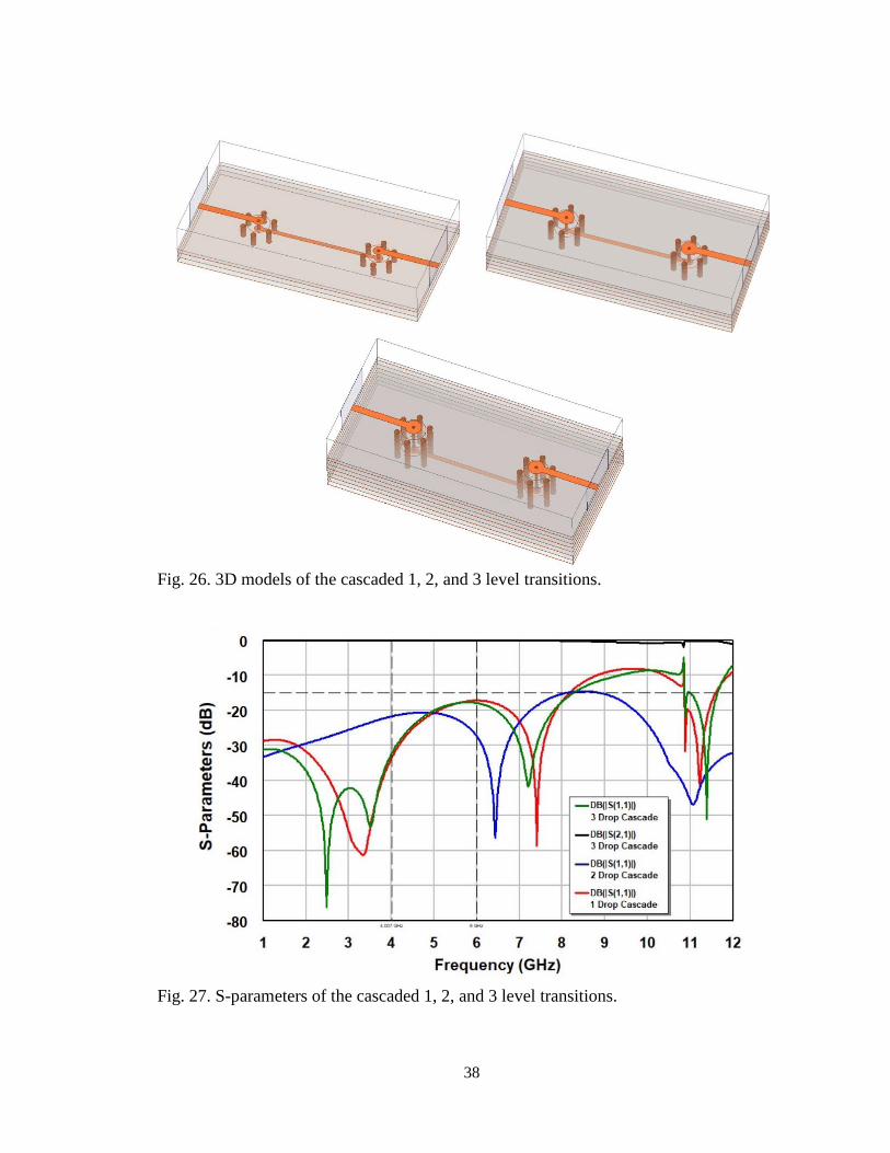
Since a trace that goes down must come back up, it is useful to also consider the
performance of two vias cascaded together. This yields insight on how a passive structure
submerged in an inner layer or a crossover of traces may perform. As shown in Fig. 26,
cascades of the optimized 1-level, 2-level, and 3-level transition were simulated. From
Fig. 27, one can see that all variations maintained a return loss of -15 dB up to 8.18 GHz.
In the filter passband of 4 GHz to 6 GHz, a return loss of less than -17.2 dB is maintained
with all the variations.
38
Fig. 26. 3D models of the cascaded 1, 2, and 3 level transitions.
Fig. 27. S-parameters of the cascaded 1, 2, and 3 level transitions.

39
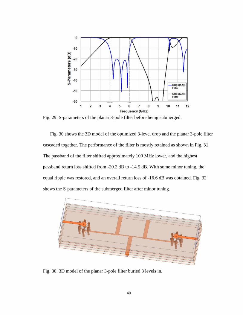
To demonstrate the effectiveness of the optimized vertical transitions, a planar 3-pole
filter submerged three levels down is simulated. This filter is shown in Fig. 28 and
consists of 3 quarter-wave short stubs inductively coupled with thin striplines. The
input/output is also inductively coupled with thin striplines. With a dielectric constant of
6.15, the overall size of the filter is 0.690” by 0.578”. Fig. 29 shows the S-parameters of
the filter and the performance specifications are summarized in Table 7.
Table 7
Filter Specifications
Center Frequency 5 GHz
1 dB Bandwidth 4 GHz to 6 GHz
Passband Return Loss <-20 dB
Size 0.690” by 0.578”
Fig. 28. Planar 3-pole filter.
40
Fig. 29. S-parameters of the planar 3-pole filter before being submerged.
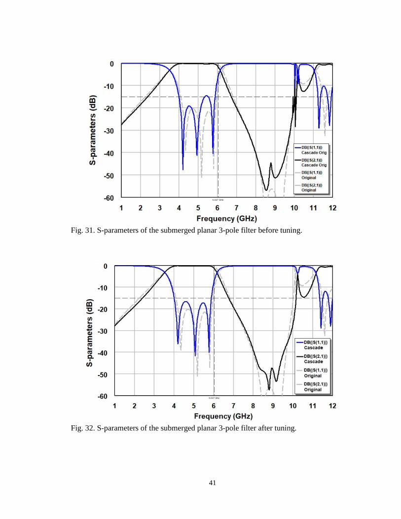
Fig. 30 shows the 3D model of the optimized 3-level drop and the planar 3-pole filter
cascaded together. The performance of the filter is mostly retained as shown in Fig. 31.
The passband of the filter shifted approximately 100 MHz lower, and the highest
passband return loss shifted from -20.2 dB to -14.5 dB. With some minor tuning, the
equal ripple was restored, and an overall return loss of -16.6 dB was obtained. Fig. 32
shows the S-parameters of the submerged filter after minor tuning.
Fig. 30. 3D model of the planar 3-pole filter buried 3 levels in.
41
Fig. 31. S-parameters of the submerged planar 3-pole filter before tuning.
Fig. 32. S-parameters of the submerged planar 3-pole filter after tuning.
42
6 CONCLUSION
EM simulation showed that for the given multilayer stack-up, 6 stitching vias
effectively shielded cavity resonance up to 9.14 GHz. Eight vias were effective up to
13.6 GHz. Using more than 8 vias would cause an intersection with the stripline; thus an
alternative stitching pattern is needed for higher frequency shielding.
In addition, time-domain reflectometry and the optimization guidelines in Table 3
were effective for minimizing the impedance mismatch caused by vias. Interestingly, an
increase in layer transitions did not correlate with performance degradation. The 1, 2, and
3 level transitions had similar performance and maintained less than -20 dB return loss up
to 7 GHz. Other publications that tested similar microstrip to stripline transitions report
similar performance. Also, the TDR was not useful for isolating each junction of the via
and one could not determine precisely which variable to change. Rather, the impedance
of the via was clumped together in the TDR.
The cascades of the 1, 2, and 3 level transitions-maintained a -15 dB return loss up to
8.18 GHz. Although, a return loss of less than -17.2 dB was maintained in the filter
passband of 4 GHz to 6 GHz, the center frequency of the filter shifted approximately
100 MHz lower. Also, the original -20 dB equal ripple return loss became distorted.
Minor tuning was required to restore the equal ripple, and a return loss of -16.6 dB was
obtained.
6.1 Future Work
This work can be continued by modeling the cavity with grounding vias rather than
the airbox. This would determine if stitching vias are able to provide proper ground to

43
lower reference planes. In addition, the conductors could be modeled to have finite
conductivity to reflect insertion loss.
To extend performance to higher frequencies, one can try using alternative pad shapes
such as a taper or bottleneck. In addition, more stitching vias and an alternative stitching
pattern could be used to obtain more shielding. Lastly, to isolate each junction of the via
in the TDR, one can try using a much faster rise-time. The last step would be to have the
design manufactured to compare measurements and simulations.
44
Literature Cited
[1] Anaren, “A Novel Surface-Mount Approach to Crossover Signals,” Microwave
Journal, 1, February 2000. [Online]. Available:
https://www.microwavejournal.com/articles/2866-a-novel-surface-mount-
approach-to-crossover-signals. [Accessed May 3, 2019].
[2] D. Packiaraj, K. J. Vinoy, P. Nagarajarao, M. Ramesh and A. T. Kalghatgi,
"Miniaturized Defected Ground High Isolation Crossovers," in IEEE Microwave
and Wireless Components Letters, vol. 23, no. 7, pp. 347-349, July 2013.
[3] P. David, Microwave Engineering. Hoboken, NJ: Wiley, 2012.
[4] Q. Tang, Y. Wang and C. Christopoulos, "Simulation and Research of the PCB
Via Effects," Third International Conference on Natural Computation (ICNC
2007), Haikou, 2007, pp. 110-114.
[5] Eurocircuits, “Making a PCB – PCB Manufacturing Step-by-Step,” Eurocircuits,
29, January 2017. [Online]. Available: https://www.eurocircuits.com/making-a-
pcb-pcb-manufacture-step-by-step/. [Accessed March 20, 2019].
[6] J. Coonrod, "High-Frequency Laminates for Hybrid Multilayer PCBs," in The
PCB Design Magazine, pp. 30-32, September 2013. [Online]. Available:
https://www.rogerscorp.com/documents/2915/acm/articles/High-Frequency-
Laminates-for-Hybrid-Multilayer-PCBs.pdf. [Accessed February 2, 2019].
[7] J. Browne, "Picking Materials for Multilayer PCBs," in Microwaves and RF, 17,
February 2011. [Online]. Available: https://www.mwrf.com/materials/picking-
materials-multilayer-pcbs. [Accessed March 13, 2019].
[8] J. Coonrod, "Navigating Multilayer Microwave PCB Tradeoffs," in Microwaves
and RF, pp. 107-114, May 2017. [Online]. Available:
https://www.rogerscorp.com/documents/2329/acm/articles/Navigating-
Multilayer-Microwave-PCB-Tradeoffs.pdf. [Accessed February 20, 2019].
[9] M. Graham, High-Speed Digital Design, a Handbook of Black Magic. Englewood
Cliffs, NJ: Prentice Hall PTR, 1993.
[10] Qiu Xiaofeng, Wu Yushu, Li Shufang, Ying Chenguang and Gao Yougang,
"Simulation and Analysis of Via Effects on High-Speed Signal Transmission on
45
PCB," 2004 Asia-Pacific Radio Science Conference, 2004. Proceedings.,
Qingdao, China, 2004, pp. 283-286.
[11] G. Dong, Y. Biao, D. Xidong and L. Yuan, "Research on the Influence of Vias on
Signal Transmission in Multilayer PCBs," 2017 13th IEEE International
Conference on Electronic Measurement & Instruments (ICEMI), Yangzhou,
2017, pp. 406-409.
[12] M. Pajovic, J. Yu and D. Milojkovic, "Analysis of Via Capacitance in Arbitrary
Multilayer PCBs," in IEEE Transactions on Electromagnetic Compatibility, vol.
49, no. 3, pp. 722-726, Aug. 2007.
[13] I. N. Ndip, W. John and H. Reichl, "RF/Microwave Modeling and Comparison of
Buried, Blind and Through Hole Vias," Proceedings of 6th Electronics Packaging
Technology Conference (EPTC 2004) (IEEE Cat. No.04EX971), Singapore, 2004,
pp. 643-648.
[14] G. Hernandez-Sosa, R. Torres-Torres and A. Sanchez, "Impedance Matching of
Traces and Multilayer Via Transitions for On-Package Links," in IEEE
Microwave and Wireless Components Letters, vol. 21, no. 11, pp. 595-597, Nov.
2011.
[15] Z. Li, P. Wang, R. Zeng and W. Zhong, "Analysis of Wideband Multilayer LTCC
Vertical Via Transition for Millimeter-Wave System-in-Package," 2017 18th
International Conference on Electronic Packaging Technology (ICEPT), Harbin,
2017, pp. 1039-1042.
[16] J. Coonrod, "Influence of Through Hole Vias on PCB RF Performance," in IPC
Apex, April 2016. [Online]. Available: https://www.rogerscorp.com. [Accessed
February 18, 2019]
[17] E. R. Pillai, "Coax Via-A Technique to Reduce Crosstalk and Enhance Impedance
Match at Vias in High-Frequency Multilayer Packages Verified by FDTD and
MoM Modeling," in IEEE Transactions on Microwave Theory and Techniques,
vol. 45, no. 10, pp. 1981-1985, Oct. 1997.
[18] Wusheng Ji, Xuedong Wang and Ying Li, "Simulation of Scattering Parameter of
Signal Via with Shielding Vias," Proceedings of 2005 IEEE International
Workshop on VLSI Design and Video Technology, 2005., Suzhou, China, 2005,
pp. 94-96.
46
[19] C. Tsai, Y. Cheng, T. Huang, Y. A. Hsu and R. Wu, "Design of Microstrip-to-
Microstrip Via Transition in Multilayered LTCC for Frequencies up to 67GHz,"
in IEEE Transactions on Components, Packaging and Manufacturing
Technology, vol. 1, no. 4, pp. 595-601, April 2011.
[20] DaeHan Kwon et al., "Characterization and Modeling of a New Via Structure in
Multilayered Printed Circuit Boards," in IEEE Transactions on Components and
Packaging Technologies, vol. 26, no. 2, pp. 483-489, June 2003.
[21] F. P. Casares-Miranda, C. Viereck, C. Camacho-Penalosa and C. Caloz, "Vertical
Microstrip Transition for Multilayer Microwave Circuits with Decoupled Passive
and Active Layers," in IEEE Microwave and Wireless Components Letters, vol.
16, no. 7, pp. 401-403, July 2006.
[22] M. Liang, Xiaoju Yu, C. Shemelya, E. MacDonald and H. Xin, "3D Printed
Multilayer Microstrip Line Structure with Vertical Transition Toward Integrated
Systems," 2015 IEEE MTT-S International Microwave Symposium, Phoenix, AZ,
2015, pp. 1-4.
[23] F. Cai, Y. Chang, K. Wang, C. Zhang, B. Wang and J. Papapolymerou, "Low-
Loss 3D Multilayer Transmission Lines and Interconnects Fabricated by Additive
Manufacturing Technologies," in IEEE Transactions on Microwave Theory and
Techniques, vol. 64, no. 10, pp. 3208-3216, Oct. 2016.


