
SHARC and the SHARC logo are registered trademarks of Analog Devices, Inc.
SHARCEmbedded Processor
ADSP-21261/ADSP-21262/ADSP-21266
Rev. G Document FeedbackInformation furnished by Analog Devices is believed to be accurate and reliable.However, no responsibility is assumed by Analog Devices for its use, nor for anyinfringements of patents or other rights of third parties that may result from its use.Specifications subject to change without notice. No license is granted by implicationor otherwise under any patent or patent rights of Analog Devices. Trademarks andregistered trademarks are the property of their respective owners.
One Technology Way, P.O. Box 9106, Norwood, MA 02062-9106 U.S.A.Tel: 781.329.4700 ©2012 Analog Devices, Inc. All rights reserved.Technical Support www.analog.com
SUMMARY
High performance 32-bit/40-bit floating-point processor optimized for high performance audio processing
Code compatibility—at assembly level, uses the same instruction set as other SHARC DSPs
Processes high performance audio while enabling low system costs
Audio decoders and postprocessor algorithms supportnonvolatile memory that can be configured to contain a combination of PCM 96 kHz, Dolby Digital, Dolby Digital Surround EX, DTS-ES Discrete 6.1, DTS-ES Matrix 6.1, DTS 96/24 5.1, MPEG2 AAC LC, MPEG2 BC 2ch, WMA-PRO V7.1, Dolby Pro Logic II, Dolby Pro Logic 2x, and DTS Neo:6
Various multichannel surround sound decoders are con-tained in ROM. For configurations of decoder algorithms, see Table 3 on Page 4.
Single-instruction multiple-data (SIMD) computational archi-tecture—two 32-bit IEEE floating-point/32-bit fixed-point/ 40-bit extended precision floating-point computational units, each with a multiplier, ALU, shifter, and register file
High bandwidth I/O—a parallel port, an SPI port, 6 serial ports, a Digital application interface (DAI), and JTAG
DAI incorporates two precision clock generators (PCGs), an input data port (IDP) that includes a parallel data acquisi-tion port (PDAP), and 3 programmable timers, all under software control by the signal routing unit (SRU)
On-chip memory—up to 2M bits on-chip SRAM and a dedi-cated 4M bits on-chip mask-programmable ROM
The ADSP-2126x processors are available with a 150 MHz or a 200 MHz core instruction rate. For complete ordering information, see Ordering Guide on Page 45.
Figure 1. Functional Block Diagram
ADDR DATA
PX REGISTER
6JTAG TEST & EMULATION
20
3
SERIAL PORTS (6)
INPUTDATA PORTS (8)PARALLEL DATA
ACQUISITION PORT
PERIPHERALTIMERS (3)
SIGNALROUTING
UNIT
PRECISION CLOCKGENERATORS (2)
DIGITAL AUDIO INTERFACE
3
16ADDRES S/
DATA BUS / GPIO
CONTROL/GPIO
PARALLELPORT
IOPREGISTERS
(MEMORY MAPPED)
CONTROL,STATUS,
DATA BUFFERS
4SPI PORT (1)
DMA CONTROLLER22 CHANNELS
4GPIO FLAGS/IRQ/TIMEXP
PROCESSINGELEMENT
(PEY)
PROCESSINGELEMENT
(PEX)
TIMERINSTRUCTION
CACHE32 � 48-BIT
DAG18 � 4 � 32
DAG28 � 4 � 32
32PM ADDRESS BUS
DM ADDRESS BUS
PM DATA BUS
DM DATA BUS
64
64
CORE PROCESSOR
PROGRAMSEQUENCER
ADDR DATA
SRAM1M BIT ROM
2M BIT
DUAL PORTED MEMORYBLOCK 0
SRAM1M BIT ROM
2M BIT
DUAL PORTED MEMORYBLOCK 1
S
IOD(32)
IOA(19)
32
I/O PROCESSOR

ADSP-21261/ADSP-21262/ADSP-21266
Rev. G | Page 2 of 48 | December 2012
TABLE OF CONTENTSSummary . . . . . . . . . . . . . . . . . . . . . . . . . . . . . . . . . . . . . . . . . . . . . . . . . . . . . . . . . . . . . . . 1General Description . . . . . . . . . . . . . . . . . . . . . . . . . . . . . . . . . . . . . . . . . . . . . . . . . 3
Family Core Architecture . . . . . . . . . . . . . . . . . . . . . . . . . . . . . . . . . . . . . . . . 3Memory and I/O Interface Features . . . . . . . . . . . . . . . . . . . . . . . . . . . 4Target Board JTAG Emulator Connector . . . . . . . . . . . . . . . . . . . . 8Development Tools . . . . . . . . . . . . . . . . . . . . . . . . . . . . . . . . . . . . . . . . . . . . . . . 8Additional Information . . . . . . . . . . . . . . . . . . . . . . . . . . . . . . . . . . . . . . . . . . 9Related Signal Chains . . . . . . . . . . . . . . . . . . . . . . . . . . . . . . . . . . . . . . . . . . . . 9
Pin Function Descriptions . . . . . . . . . . . . . . . . . . . . . . . . . . . . . . . . . . . . . . . 10Address Data Pins as Flags . . . . . . . . . . . . . . . . . . . . . . . . . . . . . . . . . . . . 13Core Instruction Rate to CLKIN Ratio Modes . . . . . . . . . . . . 13Address Data Modes . . . . . . . . . . . . . . . . . . . . . . . . . . . . . . . . . . . . . . . . . . . . 13
Product Specifications . . . . . . . . . . . . . . . . . . . . . . . . . . . . . . . . . . . . . . . . . . . . . 14Operating Conditions . . . . . . . . . . . . . . . . . . . . . . . . . . . . . . . . . . . . . . . . . . 14Electrical Characteristics . . . . . . . . . . . . . . . . . . . . . . . . . . . . . . . . . . . . . . . 14Package Information . . . . . . . . . . . . . . . . . . . . . . . . . . . . . . . . . . . . . . . . . . . 15
ESD Caution . . . . . . . . . . . . . . . . . . . . . . . . . . . . . . . . . . . . . . . . . . . . . . . . . . . . . . 15Maximum Power Dissipation . . . . . . . . . . . . . . . . . . . . . . . . . . . . . . . . . 15Absolute Maximum Ratings . . . . . . . . . . . . . . . . . . . . . . . . . . . . . . . . . . . 15Timing Specifications . . . . . . . . . . . . . . . . . . . . . . . . . . . . . . . . . . . . . . . . . . . 15Output Drive Currents . . . . . . . . . . . . . . . . . . . . . . . . . . . . . . . . . . . . . . . . . 37Test Conditions . . . . . . . . . . . . . . . . . . . . . . . . . . . . . . . . . . . . . . . . . . . . . . . . . . 37Capacitive Loading . . . . . . . . . . . . . . . . . . . . . . . . . . . . . . . . . . . . . . . . . . . . . . 37Environmental Conditions . . . . . . . . . . . . . . . . . . . . . . . . . . . . . . . . . . . . 38Thermal Characteristics . . . . . . . . . . . . . . . . . . . . . . . . . . . . . . . . . . . . . . . . 38
144-Lead LQFP Pin Configurations . . . . . . . . . . . . . . . . . . . . . . . . . . . . 39136-Ball BGA Pin Configurations . . . . . . . . . . . . . . . . . . . . . . . . . . . . . . . 40Outline Dimensions . . . . . . . . . . . . . . . . . . . . . . . . . . . . . . . . . . . . . . . . . . . . . . . . 43
Surface-Mount Design . . . . . . . . . . . . . . . . . . . . . . . . . . . . . . . . . . . . . . . . . . 44Automotive Products . . . . . . . . . . . . . . . . . . . . . . . . . . . . . . . . . . . . . . . . . . . . . . 45Ordering Guide . . . . . . . . . . . . . . . . . . . . . . . . . . . . . . . . . . . . . . . . . . . . . . . . . . . . . 45
REVISION HISTORY
12/12—Rev. F to Rev. GCorrected Long Word Memory Space in Table 4 inMemory and I/O Interface Features . . . . . . . . . . . . . . . . . . . . . . . . . . . . . . .4 Updated Development Tools . . . . . . . . . . . . . . . . . . . . . . . . . . . . . . . . . . . . . . .8 Added section, Related Signal Chains . . . . . . . . . . . . . . . . . . . . . . . . . . . . .9 Changed the package designator in Figure 36 from BC-136 to BC-136-1. This change in no way affects form, fit, or function. See Outline Dimensions . . . . . . . . . . . . . . . . . . . . . . . . . . . . . . . . . . . . . . . . . . . 43 Updated Ordering Guide . . . . . . . . . . . . . . . . . . . . . . . . . . . . . . . . . . . . . . . . . . 45

ADSP-21261/ADSP-21262/ADSP-21266
Rev. G | Page 3 of 48 | December 2012
GENERAL DESCRIPTIONThe ADSP-21261/ADSP-21262/ADSP-21266 SHARC® DSPs are members of the SIMD SHARC family of DSPs featuring Analog Devices, Inc., Super Harvard Architecture. The ADSP-2126x is source code compatible with the ADSP-21160 and ADSP-21161 DSPs as well as with first generation ADSP-2106x SHARC processors in SISD (single-instruction, single-data) mode. Like other SHARC DSPs, the ADSP-2126x are 32-bit/40-bit floating-point processors optimized for high per-formance audio applications with dual-ported on-chip SRAM, mask-programmable ROM, multiple internal buses to eliminate I/O bottlenecks, and an innovative digital application interface.Table 1 shows performance benchmarks for the processors run-ning at 200 MHz. Table 2 shows the features of the individual product offerings.
As shown in the functional block diagram in Figure 1 on Page 1, the ADSP-2126x uses two computational units to deliver a 5 to 10 times performance increase over previous SHARC proces-sors on a range of DSP algorithms. Fabricated in a state-of-the-art, high speed, CMOS process, the ADSP-2126x DSPs achieve an instruction cycle time of 5 ns at 200 MHz or 6.6 ns at 150 MHz. With its SIMD computational hardware, the ADSP-2126x can perform 1200 MFLOPS running at 200 MHz, or 900 MFLOPS running at 150 MHz.
The ADSP-2126x continues the SHARC family’s industry-lead-ing standards of integration for DSPs, combining a high performance 32-bit DSP core with integrated, on-chip system features. These features include 2M bit dual-ported SRAM memory, 4M bit dual-ported ROM, an I/O processor that sup-ports 22 DMA channels, six serial ports, an SPI interface, external parallel bus, and digital application interface. The block diagram of the ADSP-2126x on Page 1 illustrates the following architectural features:
• Two processing elements, each containing an ALU, multi-plier, shifter, and data register file
• Data address generators (DAG1, DAG2)• Program sequencer with instruction cache• PM and DM buses capable of supporting four 32-bit data
transfers between memory and the core at every core pro-cessor cycle
• Three programmable interval timers with PWM genera-tion, PWM capture/pulse width measurement, and external event counter capabilities
• On-chip dual-ported SRAM (up to 2M bit)• On-chip dual-ported, mask-programmable ROM
(up to 4M bit)• JTAG test access port• 8- or 16-bit parallel port that supports interfaces to off-chip
memory peripherals• DMA controller• Six full-duplex serial ports (four on the ADSP-21261)• SPI-compatible interface• Digital application interface that includes two precision
clock generators (PCG), an input data port (IDP), six serial ports, eight serial interfaces, a 20-bit synchronous parallel input port, 10 interrupts, six flag outputs, six flag inputs, three programmable timers, and a flexible signal routing unit (SRU)
FAMILY CORE ARCHITECTURE
The ADSP-2126x is code compatible at the assembly level with the ADSP-2136x and ADSP-2116x, and with the first generation ADSP-2106x SHARC DSPs. The ADSP-2126x shares architec-tural features with the ADSP-2136x and ADSP-2116x SIMD SHARC family of DSPs, as detailed in the following sections.
SIMD Computational Engine
The ADSP-2126x contain two computational processing ele-ments that operate as a single-instruction multiple-data (SIMD) engine. The processing elements are referred to as PEX and PEY and each contains an ALU, multiplier, shifter, and register file. PEX is always active, and PEY can be enabled by setting the PEYEN mode bit in the MODE1 register. When this mode is enabled, the same instruction is executed in both processing
Table 1. Processor Benchmarks (at 200 MHz)
Benchmark AlgorithmSpeed (at 200 MHz)
1024 Point Complex FFT (Radix 4, with reversal) 61.3 s
FIR Filter (per tap)1
1 Assumes two files in multichannel SIMD mode.
3.3 ns
IIR Filter (per biquad)1 13.3 ns
Matrix Multiply (pipelined) [3×3] × [3×1] [4×4] × [4×1]
30 ns53.3 ns
Divide (y/x) 20 ns
Inverse Square Root 30 ns
Table 2. ADSP-2126x SHARC Processor Features
Feature ADSP-21261 ADSP-21262 ADSP-21266
RAM 1M bit 2M bit 2M bit
ROM 3M bit 4M bit 4M bit
Audio Decoders in ROM1
1 For information on available audio decoding algorithms, see Table 3 on Page 4.
No No Yes
DMA Channels 18 22 22
SPORTs 4 6 6
Package 136-ball BGA144-lead LQFP
136-ball BGA144-lead LQFP
136-ball BGA144-lead LQFP

ADSP-21261/ADSP-21262/ADSP-21266
Rev. G | Page 4 of 48 | December 2012
elements, but each processing element operates on different data. This architecture is efficient at executing math intensive audio algorithms.Entering SIMD mode also has an effect on the way data is trans-ferred between memory and the processing elements. When in SIMD mode, twice the data bandwidth is required to sustain computational operation in the processing elements. Because of this requirement, entering SIMD mode also doubles the band-width between memory and the processing elements. When using the DAGs to transfer data in SIMD mode, two data values are transferred with each access of memory or the register file.
Independent, Parallel Computation Units
Within each processing element is a set of computational units. The computational units consist of an arithmetic/logic unit (ALU), multiplier, and shifter. These units perform all opera-tions in a single cycle. The three units within each processing element are arranged in parallel, maximizing computational throughput. Single multifunction instructions execute parallel ALU and multiplier operations. In SIMD mode, the parallel ALU and multiplier operations occur in both processing elements. These computation units support IEEE 32-bit single precision floating-point, 40-bit extended precision floating-point, and 32-bit fixed-point data formats.
Data Register File
A general-purpose data register file is contained in each processing element. The register files transfer data between the computation units and the data buses, and store intermediate results. These 10-port, 32-register (16 primary, 16 secondary) register files, combined with the ADSP-2126x enhanced Har-vard architecture, allow unconstrained data flow between computation units and internal memory. The registers in PEX are referred to as R0–R15 and in PEY as S0–S15.
Single-Cycle Fetch of Instruction and Four Operands
The ADSP-2126x features an enhanced Harvard architecture in which the data memory (DM) bus transfers data and the pro-gram memory (PM) bus transfers both instructions and data (see Figure 1 on Page 1). With the ADSP-2126x’s separate pro-gram and data memory buses and on-chip instruction cache, the processor can simultaneously fetch four operands (two over each data bus) and one instruction (from the cache), all in a single cycle.
Instruction Cache
The ADSP-2126x includes an on-chip instruction cache that enables three-bus operation to fetch an instruction and four data values. The cache is selective—only the instructions whose fetches conflict with PM bus data accesses are cached. This cache allows full-speed execution of core, looped operations such as digital filter multiply-accumulates, and FFT butterfly processing.
Data Address Generators with Zero-Overhead Hardware Circular Buffer Support
The ADSP-2126x’s two data address generators (DAGs) are used for indirect addressing and implementing circular data buffers in hardware. Circular buffers allow efficient program-ming of delay lines and other data structures required in digital signal processing, and are commonly used in digital filters and Fourier transforms. The two DAGs of the ADSP-2126x contain sufficient registers to allow the creation of up to 32 circular buf-fers (16 primary register sets, 16 secondary). The DAGs automatically handle address pointer wraparound, reduce over-head, increase performance, and simplify implementation. Circular buffers can start and end at any memory location.
Flexible Instruction Set
The 48-bit instruction word accommodates a variety of parallel operations for concise programming. For example, the ADSP-2126x can conditionally execute a multiply, an add, and a subtract in both processing elements while branching and fetch-ing up to four 32-bit values from memory—all in a single instruction.
MEMORY AND I/O INTERFACE FEATURES
The ADSP-2126x adds the following architectural features to the SIMD SHARC family core:
Dual-Ported On-Chip Memory
The ADSP-21262 and ADSP-21266 contain two megabits of internal SRAM and four megabits of internal mask-program-mable ROM. The ADSP-21261 contain one megabit of internal SRAM and three megabits of internal mask-programmable ROM. Each block can be configured for different combinations of code and data storage (see memory maps, Table 4 and Table 5). Each memory block is dual-ported for single-cycle, independent accesses by the core processor and I/O processor. The dual-ported memory, in combination with three separate on-chip buses, allows two data transfers from the core and one from the I/O processor, in a single cycle.The ADSP-2126x is available with a variety of multichannel surround sound decoders, preprogrammed in ROM memory. Table 3 shows the configuration of decoder algorithms.
Table 3. Multichannel Surround Sound Decoder Algorithms in On-Chip ROM
Algorithms B ROM C ROM D ROM
PCM Yes Yes Yes
AC-3 Yes Yes Yes
DTS 96/24 v2.2 v2.3 v2.3
AAC (LC) Yes Yes Coefficients only
WMAPRO 7.1 96 KHz No No Yes
MPEG2 BC 2ch Yes Yes No
Noise Yes Yes Yes
DPL2x/EX DPL2 Yes Yes
Neo:6/ES (v2.5046) Yes Yes Yes
ADSP-21261/ADSP-21262/ADSP-21266
Rev. G | Page 5 of 48 | December 2012
The ADSP-2126x’s SRAM can be configured as a maximum of 64K words of 32-bit data, 128K words of 16-bit data, 42K words of 48-bit instructions (or 40-bit data), or combinations of differ-ent word sizes up to two megabits. All of the memory can be accessed as 16-bit, 32-bit, 48-bit, or 64-bit words. A 16-bit float-ing-point storage format is supported that effectively doubles the amount of data that can be stored on-chip. Conversion between the 32-bit floating-point and 16-bit floating-point for-mats is performed in a single instruction. While each memory block can store combinations of code and data, accesses are most efficient when one block stores data using the DM bus for transfers, and the other block stores instructions and data using the PM bus for transfers.Using the DM bus and PM buses, with one dedicated to each memory block, assures single-cycle execution with two data transfers. In this case, the instruction must be available in the cache.
DMA Controller
The ADSP-2126x’s on-chip DMA controller allows zero-over-head data transfers without processor intervention. The DMA controller operates independently and invisibly to the processor core, allowing DMA operations to occur while the core is simul-taneously executing its program instructions. DMA transfers can occur between the ADSP-2126x’s internal memory and its serial ports, the SPI-compatible (serial peripheral interface) port, the IDP (input data port), parallel data acquisition port (PDAP), or the parallel port. Up to 22 channels of DMA are available on the ADSP-2126x—one for the SPI interface, 12 via the serial ports, eight via the input data port, and one via the processor’s parallel port. Programs can be downloaded to the ADSP-2126x using DMA transfers. Other DMA features include interrupt generation upon completion of DMA trans-fers, and DMA chaining for automatic linked DMA transfers.
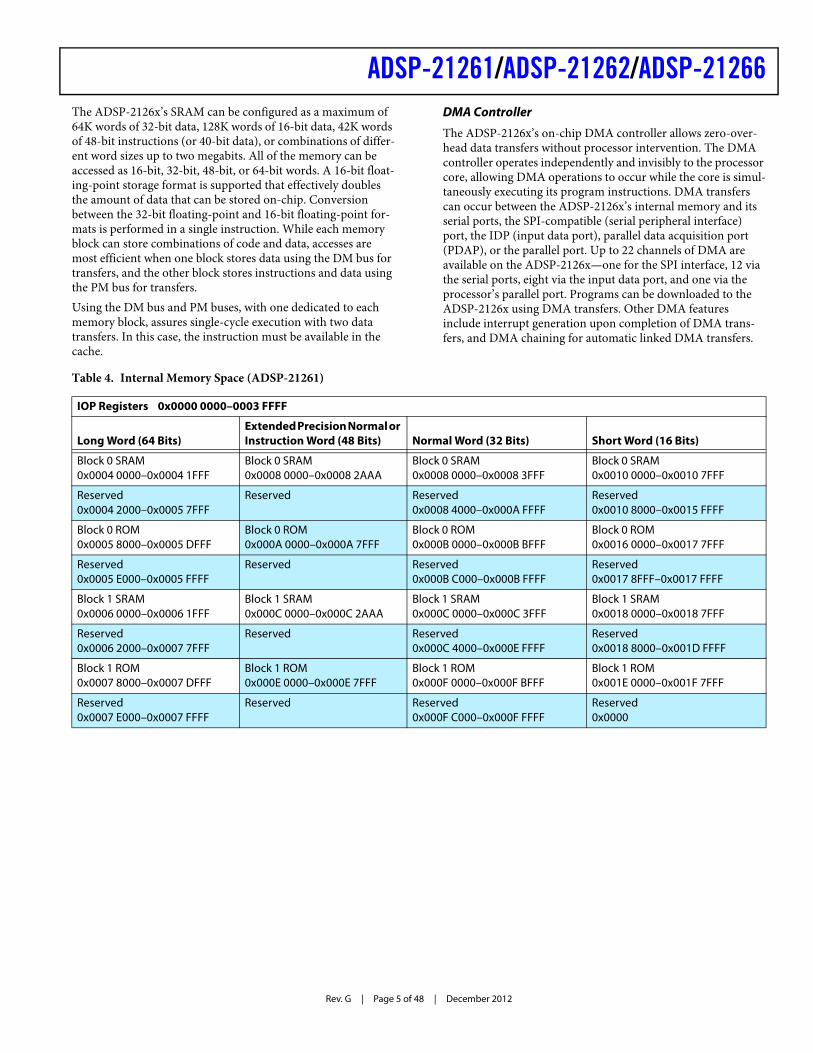
Table 4. Internal Memory Space (ADSP-21261)
IOP Registers 0x0000 0000–0003 FFFF
Long Word (64 Bits)Extended Precision Normal or Instruction Word (48 Bits) Normal Word (32 Bits) Short Word (16 Bits)
Block 0 SRAM0x0004 0000–0x0004 1FFF
Block 0 SRAM0x0008 0000–0x0008 2AAA
Block 0 SRAM0x0008 0000–0x0008 3FFF
Block 0 SRAM0x0010 0000–0x0010 7FFF
Reserved0x0004 2000–0x0005 7FFF
Reserved Reserved0x0008 4000–0x000A FFFF
Reserved0x0010 8000–0x0015 FFFF
Block 0 ROM0x0005 8000–0x0005 DFFF
Block 0 ROM0x000A 0000–0x000A 7FFF
Block 0 ROM0x000B 0000–0x000B BFFF
Block 0 ROM0x0016 0000–0x0017 7FFF
Reserved0x0005 E000–0x0005 FFFF
Reserved Reserved0x000B C000–0x000B FFFF
Reserved0x0017 8FFF–0x0017 FFFF
Block 1 SRAM0x0006 0000–0x0006 1FFF
Block 1 SRAM0x000C 0000–0x000C 2AAA
Block 1 SRAM0x000C 0000–0x000C 3FFF
Block 1 SRAM0x0018 0000–0x0018 7FFF
Reserved0x0006 2000–0x0007 7FFF
Reserved Reserved0x000C 4000–0x000E FFFF
Reserved0x0018 8000–0x001D FFFF
Block 1 ROM0x0007 8000–0x0007 DFFF
Block 1 ROM0x000E 0000–0x000E 7FFF
Block 1 ROM0x000F 0000–0x000F BFFF
Block 1 ROM0x001E 0000–0x001F 7FFF
Reserved0x0007 E000–0x0007 FFFF
Reserved Reserved0x000F C000–0x000F FFFF
Reserved0x0000
Rev. G | Page 6 of 48 | December 2012
ADSP-21261/ADSP-21262/ADSP-21266
Digital Application Interface (DAI)
The Digital application interface provides the ability to connect various peripherals to any of the SHARC DSP’s DAI pins (DAI_P20–1). Connections are made using the signal routing unit (SRU, shown in the block diagram on Page 1).The SRU is a matrix routing unit (or group of multiplexers) that enables the peripherals provided by the DAI to be intercon-nected under software control. This allows easy use of the DAI associated peripherals for a much wider variety of applications by using a larger set of algorithms than is possible with noncon-figurable signal paths.The DAI also includes six serial ports, two precision clock gen-erators (PCGs), an input data port (IDP), six flag outputs and six flag inputs, and three timers. The IDP provides an additional input path to the ADSP-2126x core, configurable as either eight channels of I2S or serial data, or as seven channels plus a single 20-bit wide synchronous parallel data acquisition port. Each data channel has its own DMA channel that is independent from the ADSP-2126x’s serial ports.For complete information on using the DAI, see the ADSP-2126x SHARC DSP Peripherals Manual.
Serial Ports
The ADSP-2126x features six full duplex synchronous serial ports that provide an inexpensive interface to a wide variety of digital and mixed-signal peripheral devices such as the Analog Devices AD183x family of audio codecs, ADCs, and DACs. The serial ports are made up of two data lines, a clock, and frame sync. The data lines can be programmed to either transmit or receive and each data line has its own dedicated DMA channel.Serial ports are enabled via 12 programmable and simultaneous receive or transmit pins that support up to 24 transmit or 24 receive channels of audio data when all six SPORTs are enabled, or six full duplex TDM streams of 128 channels per frame.
The serial ports operate at up to one-quarter of the DSP core clock rate, providing each with a maximum data rate of 50M bits/sec for a 200 MHz core and 37.5M bits/sec for a 150 MHz core. Serial port data can be automatically transferred to and from on-chip memory via a dedicated DMA. Each of the serial ports can work in conjunction with another serial port to provide TDM support. One SPORT provides two transmit sig-nals while the other SPORT provides two receive signals. The frame sync and clock are shared.Serial ports operate in four modes:
• Standard DSP serial mode• Multichannel (TDM) mode• I2S mode• Left-justified sample pair mode
Left-justified sample pair mode is a mode where in each frame sync cycle, two samples of data are transmitted/received—one sample on the high segment of the frame sync, the other on the low segment of the frame sync. Programs have control over var-ious attributes of this mode.Each of the serial ports supports the left-justified sample-pair and I2S protocols (I2S is an industry-standard interface com-monly used by audio codecs, ADCs, and DACs) with two data pins, allowing four left-justified sample-pair or I2S channels (using two stereo devices) per serial port with a maximum of up to 24 audio channels. The serial ports permit little-endian or big-endian transmission formats and word lengths selectable from 3 bits to 32 bits. For the left-justified sample pair and I2S modes, data-word lengths are selectable between 8 bits and 32 bits. Serial ports offer selectable synchronization and transmit modes as well as optional -law or A-law companding selection on a per channel basis. Serial port clocks and frame syncs can be internally or externally generated.
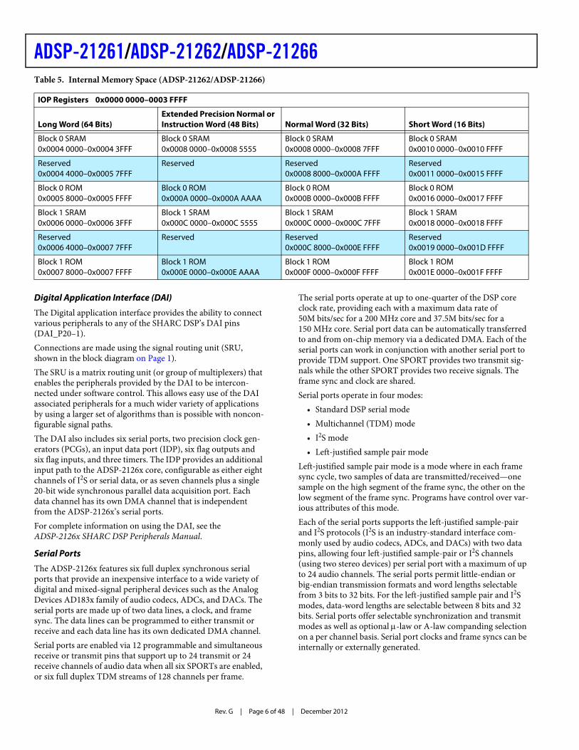
Table 5. Internal Memory Space (ADSP-21262/ADSP-21266)
IOP Registers 0x0000 0000–0003 FFFF
Long Word (64 Bits)Extended Precision Normal or Instruction Word (48 Bits) Normal Word (32 Bits) Short Word (16 Bits)
Block 0 SRAM0x0004 0000–0x0004 3FFF
Block 0 SRAM0x0008 0000–0x0008 5555
Block 0 SRAM0x0008 0000–0x0008 7FFF
Block 0 SRAM0x0010 0000–0x0010 FFFF
Reserved0x0004 4000–0x0005 7FFF
Reserved Reserved0x0008 8000–0x000A FFFF
Reserved0x0011 0000–0x0015 FFFF
Block 0 ROM0x0005 8000–0x0005 FFFF
Block 0 ROM 0x000A 0000–0x000A AAAA
Block 0 ROM0x000B 0000–0x000B FFFF
Block 0 ROM0x0016 0000–0x0017 FFFF
Block 1 SRAM0x0006 0000–0x0006 3FFF
Block 1 SRAM0x000C 0000–0x000C 5555
Block 1 SRAM0x000C 0000–0x000C 7FFF
Block 1 SRAM0x0018 0000–0x0018 FFFF
Reserved0x0006 4000–0x0007 7FFF
Reserved Reserved0x000C 8000–0x000E FFFF
Reserved0x0019 0000–0x001D FFFF
Block 1 ROM0x0007 8000–0x0007 FFFF
Block 1 ROM 0x000E 0000–0x000E AAAA
Block 1 ROM0x000F 0000–0x000F FFFF
Block 1 ROM0x001E 0000–0x001F FFFF

ADSP-21261/ADSP-21262/ADSP-21266
Rev. G | Page 7 of 48 | December 2012
Serial Peripheral (Compatible) Interface
The serial peripheral interface is an industry-standard synchro-nous serial link, enabling the ADSP-2126x SPI-compatible port to communicate with other SPI-compatible devices. SPI is an interface consisting of two data pins, one device select pin, and one clock pin. It is a full-duplex synchronous serial interface, supporting both master and slave modes. The SPI port can operate in a multimaster environment by interfacing with up to four other SPI-compatible devices, either acting as a master or slave device. The ADSP-2126x SPI-compatible peripheral implementation also features programmable baud rates at up to 50 MHz for a core clock of 200 MHz and up to 37.5 MHz for a core clock of 150 MHz, clock phases, and polarities. The ADSP-2126x SPI-compatible port uses open-drain drivers to support a multimaster configuration and to avoid data contention.
Parallel Port
The parallel port provides interfaces to SRAM and peripheral devices. The multiplexed address and data pins (AD15–0) can access 8-bit devices with up to 24 bits of address, or 16-bit devices with up to 16 bits of address. In either mode, 8- or 16-bit, the maximum data transfer rate is one-third the core clock speed. As an example, a clock rate of 200 MHz is equivalent to 66M byte/sec, and a clock rate of 150 MHz is equivalent to 50M byte/sec. DMA transfers are used to move data to and from internal memory. Access to the core is also facilitated through the paral-lel port register read/write functions. The RD, WR, and ALE (address latch enable) pins are the control pins for the parallel port.
Timers
The ADSP-2126x has a total of four timers: a core timer able to generate periodic software interrupts, and three general-pur-pose timers that can generate periodic interrupts and be independently set to operate in one of three modes:
• Pulse waveform generation mode• Pulse width count/capture mode• External event watchdog mode
The core timer can be configured to use FLAG3 as a timer expired output signal, and each general-purpose timer has one bidirectional pin and four registers that implement its mode of operation: a 6-bit configuration register, a 32-bit count register, a 32-bit period register, and a 32-bit pulse width register. A sin-gle control and status register enables or disables all three general-purpose timers independently.
ROM-Based Security
The ADSP-2126x has a ROM security feature that provides hardware support for securing user software code by preventing unauthorized reading from the internal code when enabled. When using this feature, the DSP does not boot-load any exter-nal code, executing exclusively from internal SRAM/ROM. Additionally, the DSP is not freely accessible via the JTAG port. Instead, a unique 64-bit key, which must be scanned in through
the JTAG or test access port, will be assigned to each customer. The device will ignore a wrong key. Emulation features and external boot modes are only available after the correct key is scanned.
Program Booting
The internal memory of the ADSP-2126x boots at system power-up from an 8-bit EPROM via the parallel port, an SPI master, an SPI slave, or an internal boot. Booting is determined by the boot configuration (BOOT_CFG1–0) pins.
Phase-Locked Loop
The ADSP-2126x uses an on-chip phase-locked loop (PLL) to generate the internal clock for the core. On power-up, the CLK_CFG1–0 pins are used to select ratios of 16:1, 8:1, and 3:1. After booting, numerous other ratios can be selected via soft-ware control. The ratios are made up of software configurable numerator values from 1 to 64 and software configurable divi-sor values of 2, 4, 8, and 16.
Power Supplies
The ADSP-2126x has separate power supply connections for the internal (VDDINT), external (VDDEXT), and analog (AVDD/AVSS) power supplies. The internal and analog supplies must meet the 1.2 V requirement. The external supply must meet the 3.3 V requirement. All external supply pins must be connected to the same power supply.Note that the analog supply pin (AVDD) powers the ADSP-2126x’s internal clock generator PLL. To produce a stable clock, it is recommended that PCB designs use an external filter circuit for the AVDD pin. Place the filter components as close as possible to the AVDD/AVSS pins. For an example circuit, see Figure 2. (A recommended ferrite chip is the muRata BLM18AG102SN1D). To reduce noise coupling, the PCB should use a parallel pair of power and ground planes for VDDINT and GND. Use wide traces to connect the bypass capac-itors to the analog power (AVDD) and ground (AVSS) pins. Note that the AVDD and AVSS pins specified in Figure 2 are inputs to the processor and not the analog ground plane on the board—the AVSS pin should connect directly to digital ground (GND) at the chip.
Figure 2. Analog Power Filter Circuit
HIGH-Z FERRITEBEAD CHIP
LOCATE ALL COMPONENTSCLOSE TO AVDD AND AVSS PINS
AVDD
AVSS
100nF 10nF 1nFADSP-212xx
VDDINT

Rev. G | Page 8 of 48 | December 2012
ADSP-21261/ADSP-21262/ADSP-21266TARGET BOARD JTAG EMULATOR CONNECTOR
Analog Devices DSP Tools product line of JTAG emulators uses the IEEE 1149.1 JTAG test access port of the ADSP-2126x pro-cessor to monitor and control the target board processor during emulation. Analog Devices DSP Tools product line of JTAG emulators provides emulation at full processor speed, allowing inspection and modification of memory, registers, and proces-sor stacks. The processor’s JTAG interface ensures that the emulator will not affect target system loading or timing.For complete information on Analog Devices SHARC DSP Tools product line of JTAG emulator operation, see the appro-priate emulator hardware user’s guide.
DEVELOPMENT TOOLS
Analog Devices supports its processors with a complete line of software and hardware development tools, including integrated development environments (which include CrossCore® Embed-ded Studio and/or VisualDSP++®), evaluation products, emulators, and a wide variety of software add-ins.
Integrated Development Environments (IDEs)
For C/C++ software writing and editing, code generation, and debug support, Analog Devices offers two IDEs. The newest IDE, CrossCore Embedded Studio, is based on the EclipseTM framework. Supporting most Analog Devices proces-sor families, it is the IDE of choice for future processors, including multicore devices. CrossCore Embedded Studio seamlessly integrates available software add-ins to support real time operating systems, file systems, TCP/IP stacks, USB stacks, algorithmic software modules, and evaluation hardware board support packages. For more information visit www.analog.com/cces.The other Analog Devices IDE, VisualDSP++, supports proces-sor families introduced prior to the release of CrossCore Embedded Studio. This IDE includes the Analog Devices VDK real time operating system and an open source TCP/IP stack. For more information visit www.analog.com/visualdsp. Note that VisualDSP++ will not support future Analog Devices processors.
EZ-KIT Lite Evaluation Board
For processor evaluation, Analog Devices provides wide range of EZ-KIT Lite® evaluation boards. Including the processor and key peripherals, the evaluation board also supports on-chip emulation capabilities and other evaluation and development features. Also available are various EZ-Extenders®, which are daughter cards delivering additional specialized functionality, including audio and video processing. For more information visit www.analog.com and search on “ezkit” or “ezextender”.
EZ-KIT Lite Evaluation Kits
For a cost-effective way to learn more about developing with Analog Devices processors, Analog Devices offer a range of EZ-KIT Lite evaluation kits. Each evaluation kit includes an EZ-KIT Lite evaluation board, directions for downloading an evaluation version of the available IDE(s), a USB cable, and a power supply.
The USB controller on the EZ-KIT Lite board connects to the USB port of the user’s PC, enabling the chosen IDE evaluation suite to emulate the on-board processor in-circuit. This permits the customer to download, execute, and debug programs for the EZ-KIT Lite system. It also supports in-circuit programming of the on-board Flash device to store user-specific boot code, enabling standalone operation. With the full version of Cross-Core Embedded Studio or VisualDSP++ installed (sold separately), engineers can develop software for supported EZ-KITs or any custom system utilizing supported Analog Devices processors.
Software Add-Ins for CrossCore Embedded Studio
Analog Devices offers software add-ins which seamlessly inte-grate with CrossCore Embedded Studio to extend its capabilities and reduce development time. Add-ins include board support packages for evaluation hardware, various middleware pack-ages, and algorithmic modules. Documentation, help, configuration dialogs, and coding examples present in these add-ins are viewable through the CrossCore Embedded Studio IDE once the add-in is installed.
Board Support Packages for Evaluation Hardware
Software support for the EZ-KIT Lite evaluation boards and EZ-Extender daughter cards is provided by software add-ins called Board Support Packages (BSPs). The BSPs contain the required drivers, pertinent release notes, and select example code for the given evaluation hardware. A download link for a specific BSP is located on the web page for the associated EZ-KIT or EZ-Extender product. The link is found in the Product Download area of the product web page.
Middleware Packages
Analog Devices separately offers middleware add-ins such as real time operating systems, file systems, USB stacks, and TCP/IP stacks. For more information see the following web pages:
• www.analog.com/ucos3• www.analog.com/ucfs• www.analog.com/ucusbd• www.analog.com/lwip
Algorithmic Modules
To speed development, Analog Devices offers add-ins that per-form popular audio and video processing algorithms. These are available for use with both CrossCore Embedded Studio and VisualDSP++. For more information visit www.analog.com and search on “Blackfin software modules” or “SHARC software modules”.
Designing an Emulator-Compatible DSP Board (Target)
For embedded system test and debug, Analog Devices provides a family of emulators. On each JTAG DSP, Analog Devices sup-plies an IEEE 1149.1 JTAG Test Access Port (TAP). In-circuit emulation is facilitated by use of this JTAG interface. The emu-lator accesses the processor’s internal features via the processor’s TAP, allowing the developer to load code, set

ADSP-21261/ADSP-21262/ADSP-21266
Rev. G | Page 9 of 48 | December 2012
breakpoints, and view variables, memory, and registers. The processor must be halted to send data and commands, but once an operation is completed by the emulator, the DSP system is set to run at full speed with no impact on system timing. The emu-lators require the target board to include a header that supports connection of the DSP’s JTAG port to the emulator.For details on target board design issues including mechanical layout, single processor connections, signal buffering, signal ter-mination, and emulator pod logic, see the EE-68: Analog Devices JTAG Emulation Technical Reference on the Analog Devices website (www.analog.com)—use site search on “EE-68.” This document is updated regularly to keep pace with improvements to emulator support.
ADDITIONAL INFORMATION
This data sheet provides a general overview of the ADSP-2126x architecture and functionality. For detailed information on the ADSP-2126x family core architecture and instruction set, refer to the ADSP-2126x SHARC DSP Core Manual and the ADSP-21160 SHARC DSP Instruction Set Reference.
RELATED SIGNAL CHAINS
A signal chain is a series of signal-conditioning electronic com-ponents that receive input (data acquired from sampling either real-time phenomena or from stored data) in tandem, with the output of one portion of the chain supplying input to the next. Signal chains are often used in signal processing applications to gather and process data or to apply system controls based on analysis of real-time phenomena. For more information about this term and related topics, see the “signal chain” entry in Wikipedia or the Glossary of EE Terms on the Analog Devices website.Analog Devices eases signal processing system development by providing signal processing components that are designed to work together well. A tool for viewing relationships between specific applications and related components is available on the www.analog.com website.The Application Signal Chains page in the Circuits from the LabTM site (http://www.analog.com/signal chains) provides:
• Graphical circuit block diagram presentation of signal chains for a variety of circuit types and applications
• Drill down links for components in each chain to selection guides and application information
• Reference designs applying best practice design techniques
Rev. G | Page 10 of 48 | December 2012
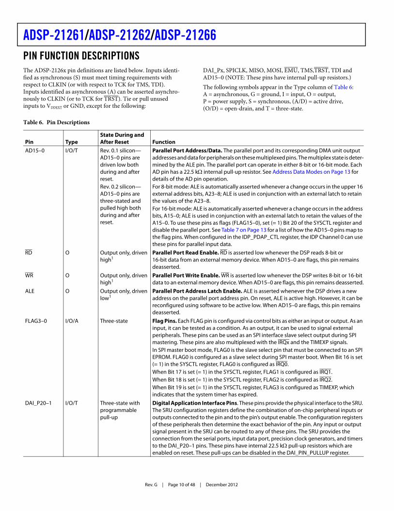
ADSP-21261/ADSP-21262/ADSP-21266PIN FUNCTION DESCRIPTIONSThe ADSP-2126x pin definitions are listed below. Inputs identi-fied as synchronous (S) must meet timing requirements with respect to CLKIN (or with respect to TCK for TMS, TDI). Inputs identified as asynchronous (A) can be asserted asynchro-nously to CLKIN (or to TCK for TRST). Tie or pull unused inputs to VDDEXT or GND, except for the following:
DAI_Px, SPICLK, MISO, MOSI, EMU, TMS,TRST, TDI and AD15–0 (NOTE: These pins have internal pull-up resistors.)The following symbols appear in the Type column of Table 6: A = asynchronous, G = ground, I = input, O = output, P = power supply, S = synchronous, (A/D) = active drive, (O/D) = open-drain, and T = three-state.
Table 6. Pin Descriptions
Pin TypeState During and After Reset Function
AD15–0 I/O/T Rev. 0.1 silicon— AD15–0 pins are driven low both during and after reset.Rev. 0.2 silicon— AD15–0 pins are three-stated and pulled high both during and after reset.
Parallel Port Address/Data. The parallel port and its corresponding DMA unit output addresses and data for peripherals on these multiplexed pins. The multiplex state is deter-mined by the ALE pin. The parallel port can operate in either 8-bit or 16-bit mode. Each AD pin has a 22.5 k internal pull-up resistor. See Address Data Modes on Page 13 for details of the AD pin operation.For 8-bit mode: ALE is automatically asserted whenever a change occurs in the upper 16 external address bits, A23–8; ALE is used in conjunction with an external latch to retain the values of the A23–8.For 16-bit mode: ALE is automatically asserted whenever a change occurs in the address bits, A15–0; ALE is used in conjunction with an external latch to retain the values of the A15–0. To use these pins as flags (FLAG15–0), set (= 1) Bit 20 of the SYSCTL register and disable the parallel port. See Table 7 on Page 13 for a list of how the AD15–0 pins map to the flag pins. When configured in the IDP_PDAP_CTL register, the IDP Channel 0 can use these pins for parallel input data.
RD O Output only, driven high1
Parallel Port Read Enable. RD is asserted low whenever the DSP reads 8-bit or 16-bit data from an external memory device. When AD15–0 are flags, this pin remains deasserted.
WR O Output only, driven high1
Parallel Port Write Enable. WR is asserted low whenever the DSP writes 8-bit or 16-bit data to an external memory device. When AD15–0 are flags, this pin remains deasserted.
ALE O Output only, driven low1
Parallel Port Address Latch Enable. ALE is asserted whenever the DSP drives a new address on the parallel port address pin. On reset, ALE is active high. However, it can be reconfigured using software to be active low. When AD15–0 are flags, this pin remains deasserted.
FLAG3–0 I/O/A Three-state Flag Pins. Each FLAG pin is configured via control bits as either an input or output. As an input, it can be tested as a condition. As an output, it can be used to signal external peripherals. These pins can be used as an SPI interface slave select output during SPI mastering. These pins are also multiplexed with the IRQx and the TIMEXP signals.In SPI master boot mode, FLAG0 is the slave select pin that must be connected to an SPI EPROM. FLAG0 is configured as a slave select during SPI master boot. When Bit 16 is set (= 1) in the SYSCTL register, FLAG0 is configured as IRQ0.When Bit 17 is set (= 1) in the SYSCTL register, FLAG1 is configured as IRQ1.When Bit 18 is set (= 1) in the SYSCTL register, FLAG2 is configured as IRQ2.When Bit 19 is set (= 1) in the SYSCTL register, FLAG3 is configured as TIMEXP, which indicates that the system timer has expired.
DAI_P20–1 I/O/T Three-state with programmable pull-up
Digital Application Interface Pins. These pins provide the physical interface to the SRU. The SRU configuration registers define the combination of on-chip peripheral inputs or outputs connected to the pin and to the pin’s output enable. The configuration registers of these peripherals then determine the exact behavior of the pin. Any input or output signal present in the SRU can be routed to any of these pins. The SRU provides the connection from the serial ports, input data port, precision clock generators, and timers to the DAI_P20–1 pins. These pins have internal 22.5 k pull-up resistors which are enabled on reset. These pull-ups can be disabled in the DAI_PIN_PULLUP register.

ADSP-21261/ADSP-21262/ADSP-21266
Rev. G | Page 11 of 48 | December 2012
SPICLK I/O Three-state with pull-up enabled, driven high in SPI-master boot mode
Serial Peripheral Interface Clock Signal. Driven by the master, this signal controls the rate at which data is transferred. The master can transmit data at a variety of baud rates. SPICLK cycles once for each bit transmitted. SPICLK is a gated clock that is active during data transfers, only for the length of the transferred word. Slave devices ignore the serial clock if the slave select input is driven inactive (HIGH). SPICLK is used to shift out and shift in the data driven on the MISO and MOSI lines. The data is always shifted out on one clock edge and sampled on the opposite edge of the clock. Clock polarity and clock phase relative to data are programmable into the SPICTL control register and define the transfer format. SPICLK has a 22.5 k internal pull-up resistor. If SPI master boot mode is selected, MOSI and SPICLK pins are driven during reset. These pins are not three-stated during reset in SPI master boot mode.
SPIDS I Input only Serial Peripheral Interface Slave Device Select. An active low signal used to select the DSP as an SPI slave device. This input signal behaves like a chip select, and is provided by the master device for the slave devices. In multimaster mode, the DSP’s SPIDS signal can be driven by a slave device to signal to the DSP (as SPI master) that an error has occurred, as some other device is also trying to be the master device. If asserted low when the device is in master mode, it is considered a multimaster error. For a single master, multiple-slave configuration where flag pins are used, this pin must be tied or pulled high to VDDEXT on the master device. For ADSP-2126x to ADSP-2126x SPI interaction, any of the master ADSP-2126x’s flag pins can be used to drive the SPIDS signal on the ADSP-2126x SPI slave device.
MOSI I/O (O/D) Three-state with pull-up enabled, driven low in SPI-master boot mode
SPI Master Out Slave In. If the ADSP-2126x is configured as a master, the MOSI pin becomes a data transmit (output) pin, transmitting output data. If the ADSP-2126x is configured as a slave, the MOSI pin becomes a data receive (input) pin, receiving input data. In an ADSP-2126x SPI interconnection, the data is shifted out from the MOSI output pin of the master and shifted into the MOSI input(s) of the slave(s). MOSI has a 22.5 k internal pull-up resistor. If SPI master boot mode is selected, MOSI and SPICLK pins are driven during reset. These pins are not three-stated during reset in SPI master boot mode.
MISO I/O (O/D) Three-state with pull-up enabled
SPI Master In Slave Out. If the ADSP-2126x is configured as a master, the MISO pin becomes a data receive (input) pin, receiving input data. If the ADSP-2126x is configured as a slave, the MISO pin becomes a data transmit (output) pin, transmitting output data. In an ADSP-2126x SPI interconnection, the data is shifted out from the MISO output pin of the slave and shifted into the MISO input pin of the master. MISO has a 22.5 k internal pull-up resistor. MISO can be configured as O/D by setting the OPD bit in the SPICTL register.Note: Only one slave is allowed to transmit data at any given time. To enable broadcast transmission to multiple SPI slaves, the DSP’s MISO pin can be disabled by setting (= 1) Bit 5 (DMISO) of the SPICTL register.
BOOT_CFG1–0 I Input only Boot Configuration Select. Selects the boot mode for the DSP. The BOOT_CFG pins must be valid before reset is asserted. See Table 8 on Page 13 for a description of the boot modes.
CLKIN I Input only Local Clock In. Used in conjunction with XTAL. CLKIN is the ADSP-2126x clock input. It configures the ADSP-2126x to use either its internal clock generator or an external clock source. Connecting the necessary components to CLKIN and XTAL enables the internal clock generator. Connecting the external clock to CLKIN while leaving XTAL unconnected configures the ADSP-2126x to use the external clock source such as an external clock oscillator. The core is clocked either by the PLL output or this clock input depending on the CLK_CFG1–0 pin settings. CLKIN should not be halted, changed, or operated below the specified frequency.
XTAL O Output only2 Crystal Oscillator Terminal. Used in conjunction with CLKIN to drive an external crystal.
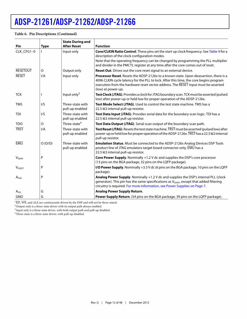
Table 6. Pin Descriptions (Continued)
Pin TypeState During and After Reset Function
Rev. G | Page 12 of 48 | December 2012
ADSP-21261/ADSP-21262/ADSP-21266
CLK_CFG1–0 I Input only Core/CLKIN Ratio Control. These pins set the start up clock frequency. See Table 9 for a description of the clock configuration modes. Note that the operating frequency can be changed by programming the PLL multiplier and divider in the PMCTL register at any time after the core comes out of reset.
RESETOUT O Output only Reset Out. Drives out the core reset signal to an external device.
RESET I/A Input only Processor Reset. Resets the ADSP-2126x to a known state. Upon deassertion, there is a 4096 CLKIN cycle latency for the PLL to lock. After this time, the core begins program execution from the hardware reset vector address. The RESET input must be asserted (low) at power-up.
TCK I Input only3 Test Clock (JTAG). Provides a clock for JTAG boundary scan. TCK must be asserted (pulsed low) after power-up or held low for proper operation of the ADSP-2126x.
TMS I/S Three-state with pull-up enabled
Test Mode Select (JTAG). Used to control the test state machine. TMS has a 22.5 k internal pull-up resistor.
TDI I/S Three-state with pull-up enabled
Test Data Input (JTAG). Provides serial data for the boundary scan logic. TDI has a 22.5 k internal pull-up resistor.
TDO O Three-state4 Test Data Output (JTAG). Serial scan output of the boundary scan path.
TRST I/A Three-state with pull-up enabled
Test Reset (JTAG). Resets the test state machine. TRST must be asserted (pulsed low) after power-up or held low for proper operation of the ADSP-2126x. TRST has a 22.5 k internal pull-up resistor.
EMU O (O/D) Three-state with pull-up enabled
Emulation Status. Must be connected to the ADSP-2126x Analog Devices DSP Tools product line of JTAG emulators target board connector only. EMU has a 22.5 k internal pull-up resistor.
VDDINT P Core Power Supply. Nominally +1.2 V dc and supplies the DSP’s core processor (13 pins on the BGA package, 32 pins on the LQFP package).
VDDEXT P I/O Power Supply. Nominally +3.3 V dc (6 pins on the BGA package, 10 pins on the LQFP package).
AVDD P Analog Power Supply. Nominally +1.2 V dc and supplies the DSP’s internal PLL (clock generator). This pin has the same specifications as VDDINT, except that added filtering circuitry is required. For more information, see Power Supplies on Page 7.
AVSS G Analog Power Supply Return.
GND G Power Supply Return. (54 pins on the BGA package, 39 pins on the LQFP package).1 RD, WR, and ALE are continuously driven by the DSP and will not be three-stated.2 Output only is a three-state driver with its output path always enabled.3 Input only is a three-state driver, with both output path and pull-up disabled.4 Three-state is a three-state driver, with pull-up disabled.
Table 6. Pin Descriptions (Continued)
Pin TypeState During and After Reset Function

ADSP-21261/ADSP-21262/ADSP-21266
Rev. G | Page 13 of 48 | December 2012
ADDRESS DATA PINS AS FLAGS
To use these pins as flags (FLAG15–0), set (= 1) Bit 20 of the SYSCTL register and disable the parallel port.
Boot Modes
CORE INSTRUCTION RATE TO CLKIN RATIO MODES
ADDRESS DATA MODES
Table 10 shows the functionality of the AD pins for 8-bit and 16-bit transfers to the parallel port. For 8-bit data transfers, ALE latches address bits A23–A8 when asserted, followed by address bits A7–A0 and data bits D7–D0 when deasserted. For 16-bit data transfers, ALE latches address bits A15–A0 when asserted, followed by data bits D15–D0 when deasserted.
Table 7. AD15–0 to FLAG Pin Mapping
AD Pin Flag Pin AD Pin Flag Pin
AD0 FLAG8 AD8 FLAG0
AD1 FLAG9 AD9 FLAG1
AD2 FLAG10 AD10 FLAG2
AD3 FLAG11 AD11 FLAG3
AD4 FLAG12 AD12 FLAG4
AD5 FLAG13 AD13 FLAG5
AD6 FLAG14 AD14 FLAG6
AD7 FLAG15 AD15 FLAG7
Table 8. Boot Mode Selection
BOOT_CFG1–0 Booting Mode
00 SPI Slave Boot
01 SPI Master Boot
10 Parallel Port Boot via EPROM
11 Reserved
Table 9. Core Instruction Rate/CLKIN Ratio Selection
CLK_CFG1–0 Core to CLKIN Ratio
00 3:1
01 16:1
10 8:1
11 Reserved
Table 10. Address/Data Mode Selection
EP Data Mode ALE
AD7–0 Function
AD15–8 Function
8-bit Asserted A15–8 A23–16
8-bit Deasserted D7–0 A7–0
16-bit Asserted A7–0 A15–8
16-bit Deasserted D7–0 D15–8

Rev. G | Page 14 of 48 | December 2012
ADSP-21261/ADSP-21262/ADSP-21266PRODUCT SPECIFICATIONSOPERATING CONDITIONS
ELECTRICAL CHARACTERISTICS
Parameter1
1 Specifications subject to change without notice.
Description Min Max Unit
VDDINT Internal (Core) Supply Voltage 1.14 1.26 V
AVDD Analog (PLL) Supply Voltage 1.14 1.26 V
VDDEXT External (I/O) Supply Voltage 3.13 3.47 V
VIH High Level Input Voltage2 @ VDDEXT = Max
2 Applies to input and bidirectional pins: AD15–0, FLAG3–0, DAI_Px, SPICLK, MOSI, MISO, SPIDS, BOOT_CFGx, CLK_CFGx, RESET, TCK, TMS, TDI, TRST.
2.0 VDDEXT + 0.5 V
VIL Low Level Input Voltage2 @ VDDEXT = Min –0.5 +0.8 V
VIH_CLKIN High Level Input Voltage3 @ VDDEXT = Max
3 Applies to input pin CLKIN.
1.74 VDDEXT + 0.5 V
VIL_CLKIN Low Level Input Voltage @ VDDEXT = Min –0.5 +1.19 V
TAMB K Grade Ambient Operating Temperature4, 5
4 See Thermal Characteristics on Page 38 for information on thermal specifications.5 See Engineer-to-Engineer Note (No. EE-216) for further information.
0 +70 C
TAMB B Grade Ambient Operating Temperature4, 5 –40 +85 C
Parameter1 Description Test Conditions Min Max Unit
VOH High Level Output Voltage2 @ VDDEXT = Min, IOH = –1.0 mA3 2.4 V
VOL Low Level Output Voltage2 @ VDDEXT = Min, IOL = 1.0 mA3 0.4 V
IIH High Level Input Current4, 5 @ VDDEXT = Max, VIN = VDDEXT Max 10 μA
IIL Low Level Input Current4 @ VDDEXT = Max, VIN = 0 V 10 μA
IILPU Low Level Input Current Pull-Up5 @ VDDEXT = Max, VIN = 0 V 200 μA
IOZH Three-State Leakage Current 6, 7, 8 @ VDDEXT = Max, VIN = VDDEXT Max 10 μA
IOZL Three-State Leakage Current6 @ VDDEXT = Max, VIN = 0 V 10 μA
IOZLPU Three-State Leakage Current Pull-Up7 @ VDDEXT = Max, VIN = 0 V 200 μA
IDD-INTYP Supply Current (Internal)9, 10, 11 tCCLK = 5.0 ns, VDDINT = 1.2 V, TAMB = +25C 500 mA
IAVDD Supply Current (Analog)11 AVDD = Max 10 mA
CIN Input Capacitance12, 13 fIN = 1 MHz, TCASE = 25°C, VIN = 1.2 V 4.7 pF1 Specifications subject to change without notice.2 Applies to output and bidirectional pins: AD15–0, RD, WR, ALE, FLAG3–0, DAI_Px, SPICLK, MOSI, MISO, EMU, TDO, CLKOUT, XTAL.3 See Output Drive Currents on Page 37 for typical drive current capabilities.4 Applies to input pins: SPIDS, BOOT_CFGx, CLK_CFGx, TCK, RESET, CLKIN.5 Applies to input pins with 22.5 k internal pull-ups: TRST, TMS, TDI.6 Applies to three-statable pins: FLAG3–0.7 Applies to three-statable pins with 22.5 k pull-ups: AD15–0, DAI_Px, SPICLK, MISO, MOSI.8 Applies to open-drain output pins: EMU, MISO, MOSI.9 Typical internal current data reflects nominal operating conditions.10 See Engineer-to-Engineer Note (EE-216) for further information.11 Characterized, but not tested.12 Applies to all signal pins.13 Guaranteed, but not tested.

ADSP-21261/ADSP-21262/ADSP-21266
Rev. G | Page 15 of 48 | December 2012
PACKAGE INFORMATION
The information presented in Figure 3 provides details about the package branding for the ADSP-21266 processors. For a complete listing of product availability, see Ordering Guide on Page 45.
ESD CAUTION
MAXIMUM POWER DISSIPATION
See Estimating Power for the ADSP-21262 SHARC Processors (EE-216) for detailed thermal and power information regarding maximum power dissipation. For information on package ther-mal specifications, see Thermal Characteristics on Page 38.
ABSOLUTE MAXIMUM RATINGS
Stresses greater than those listed in Table 12 may cause perma-nent damage to the device. These are stress ratings only; functional operation of the device at these or any other condi-tions greater than those indicated in the operational sections of
this specification is not implied. Exposure to absolute maximum rating conditions for extended periods may affect device reliability.
TIMING SPECIFICATIONS
Use the exact timing information given. Do not attempt to derive parameters from the addition or subtraction of others. While addition or subtraction would yield meaningful results for an individual device, the values given in this data sheet reflect statistical variations and worst cases. Consequently, it is not meaningful to add parameters to derive longer times.Timing requirements apply to signals that are controlled by cir-cuitry external to the processor, such as the data input for a read operation. Timing requirements guarantee that the processor operates correctly with other devices.Switching characteristics specify how the processor changes its signals. Circuitry external to the processor must be designed for compatibility with these signal characteristics. Switching char-acteristics describe what the processor will do in a given circumstance. Use switching characteristics to ensure that any timing requirement of a device connected to the processor (such as memory) is satisfied.
Core Clock Requirements
The processor’s internal clock (a multiple of CLKIN) provides the clock signal for timing internal memory, processor core, serial ports, and parallel port (as required for read/write strobes in asynchronous access mode). During reset, program the ratio between the DSP’s internal clock frequency and external (CLKIN) clock frequency with the CLK_CFG1–0 pins. To determine switching frequencies for the serial ports, divide down the internal clock, using the programmable divider con-trol of each port (DIVx for the serial ports). The processor’s internal clock switches at higher frequencies than the system input clock (CLKIN). To generate the internal clock, the DSP uses an internal phase-locked loop (PLL). This PLL-based clocking minimizes the skew between the system clock (CLKIN) signal and the DSP’s internal clock (the clock source for the parallel port logic and I/O pads).
Figure 3. Typical Package Brand
Table 11. Package Brand Information
Brand Key Field Description
t Temperature Range
pp Package Type
Z RoHS Compliant Option (optional)
cc See Ordering Guide
vvvvvv.x Assembly Lot Code
n.n Silicon Revision
# RoHS Compliant Designation
yyww Date Code
vvvvvv.x n.n
tppZ-cc
S
ADSP-2126x
a
#yyww country_of_origin
ESD (electrostatic discharge) sensitive device.Charged devices and circuit boards can discharge without detection. Although this product features patented or proprietary protection circuitry, damage may occur on devices subjected to high energy ESD. Therefore, proper ESD precautions should be taken to avoid performance degradation or loss of functionality.
Table 12. Absolute Maximum Ratings
Parameter Rating
Internal (Core) Supply Voltage (VDDINT) –0.3 V to +1.4 V
Analog (PLL) Supply Voltage (AVDD) –0.3 V to +1.4 V
External (I/O) Supply Voltage (VDDEXT) –0.3 V to +3.8 V
Input Voltage –0.5 V to VDDEXT +0.5 V
Output Voltage Swing –0.5 V to VDDEXT +0.5 V
Load Capacitance 200 pF
Storage Temperature Range –65C to +150CJunction Temperature Under Bias 125C

Rev. G | Page 16 of 48 | December 2012
ADSP-21261/ADSP-21262/ADSP-21266Voltage Controlled OscillatorIn application designs, the PLL multiplier value should be selected in such a way that the VCO frequency never exceeds fVCO specified in Table 16.
• The product of CLKIN and PLLM must never exceed 1/2 of fVCO (max) in Table 16 if the input divider is not enabled (INDIV = 0).
• The product of CLKIN and PLLM must never exceed fVCO (max) in Table 16 if the input divider is enabled (INDIV = 1).
The VCO frequency is calculated as follows:fVCO = 2 PLLM fINPUTfCCLK = (2 PLLM fINPUT) (2 PLLD)where:fVCO = VCO outputPLLM = Multiplier value programmed in the PMCTL register. During reset, the PLLM value is derived from the ratio selected using the CLK_CFG pins in hardware.PLLD = 2, 4, 8, 16 based on the PLLD value programmed on the PMCTL register. During reset this value is 1.fINPUT = is the input frequency to the PLL.fINPUT = CLKIN when the input divider is disabled orfINPUT = CLKIN 2 when the input divider is enabledNote the definitions of various clock periods that are a function of CLKIN and the appropriate ratio control shown in Table 13 and Table 14.
Figure 4 shows core to CLKIN relationships with external oscil-lator or crystal. The shaded divider/multiplier blocks denote where clock ratios can be set through hardware or software using the power management control register (PMCTL). For more information, see the ADSP-2126x SHARC Processor Peripherals Reference and Managing the Core PLL on Third-Generation SHARC Processors (EE-290).
Table 13. CLKOUT and CCLK Clock Generation Operation
Timing Requirements Description Calculation
CLKIN Input Clock 1/tCK
CCLK Core Clock Variable, see equation
Table 14. Clock Periods
Timing Requirements Description1
tCK CLKIN Clock Period
tCCLK (Processor) Core Clock Period
tMCLK Internal memory clock = 1/2 tCCLK
tSCLK Serial Port Clock Period = (tCCLK) × SR
tSPICLK SPI Clock Period = (tCCLK) × SPIR1 where:
SR = serial port-to-core clock ratio (wide range, determined by SPORT CLKDIV)SPIR = SPI-to-core clock ratio (wide range, determined by SPIBAUD register)SCLK = serial port clockSPICLK = SPI clock
Figure 4. Core Clock and System Clock Relationship to CLKIN
LOOPFILTER
CLKIN
CCLK
PLL
XTAL
CLKINDIVIDER
RESETOUTDELAY OF4096 CLKIN
CYCLESRESET
PLLMULTIPLIER
BUF
VCO
BUF
PLLICLK
PMCTL CLK_CFGx/PMCTL
PLLDIVIDER
CLK_CFGx/PMCTL
MU
XP
INM
UX
DIVIDEBY 2
RESETOUT
PMCTL
CLKOUT (TEST ONLY)
MCLK
CORERST

ADSP-21261/ADSP-21262/ADSP-21266
Rev. G | Page 17 of 48 | December 2012
Power-Up Sequencing
The timing requirements for DSP startup are given in Table 15 and Figure 5. Note that during power-up, a leakage current of approximately 200 A may be observed on the RESET pin. This leakage current results from the weak internal pull-up resistor on this pin being enabled during power-up.
Table 15. Power-Up Sequencing (DSP Startup)
Parameter Min Max Unit
Timing Requirements
tRSTVDD RESET Low Before VDDINT/VDDEXT On 0 ns
tIVDDEVDD VDDINT On Before VDDEXT –50 +200 ms
tCLKVDD CLKIN Valid After VDDINT/VDDEXT Valid1 0 200 ms
tCLKRST CLKIN Valid Before RESET Deasserted 102 μs
tPLLRST PLL Control Setup Before RESET Deasserted 203 μs
Switching Characteristics
tCORERST DSP Core Reset Deasserted After RESET Deasserted 4096 tCK4, 5
1 Valid VDDINT/VDDEXT assumes that the supplies are fully ramped to their 1.2 V and 3.3 V rails. Voltage ramp rates can vary from microseconds to hundreds of milliseconds depending on the design of the power supply subsystem.
2 Assumes a stable CLKIN signal, after meeting worst-case startup timing of crystal oscillators. Refer to the crystal oscillator manufacturer’s data sheet for startup time. Assume a 25 ms maximum oscillator startup time if using the XTAL pin and internal oscillator circuit in conjunction with an external crystal.
3 Based on CLKIN cycles.4 Applies after the power-up sequence is complete. Subsequent resets require a minimum of four CLKIN cycles for RESET to be held low in order to properly initialize and
propagate default states at all I/O pins.5 The 4096 cycle count depends on tSRST specification in Table 17. If setup time is not met, one additional CLKIN cycle can be added to the core reset time, resulting in 4097
cycles maximum.
Figure 5. Power-Up Sequencing
tRSTVDD
tCLKVDD
tCLKRST
tCORERSTtPLLRST
VDDEXT
VDDINT
CLKIN
CLK_CFG1–0
RESET
RESETOUT(MUXED WITH CLKOUT)
tIVDDEVDD
Rev. G | Page 18 of 48 | December 2012
ADSP-21261/ADSP-21262/ADSP-21266Clock Input
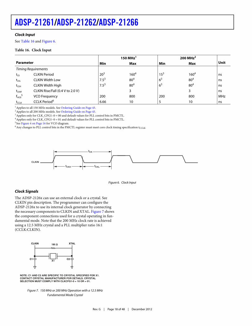
See Table 16 and Figure 6.
Clock Signals
The ADSP-2126x can use an external clock or a crystal. See CLKIN pin description. The programmer can configure the ADSP-2126x to use its internal clock generator by connecting the necessary components to CLKIN and XTAL. Figure 7 shows the component connections used for a crystal operating in fun-damental mode. Note that the 200 MHz clock rate is achieved using a 12.5 MHz crystal and a PLL multiplier ratio 16:1 (CCLK:CLKIN).
Table 16. Clock Input
Parameter150 MHz1 200 MHz2
UnitMin Max Min Max
Timing Requirements
tCK CLKIN Period 203 1604 153 1604 ns
tCKL CLKIN Width Low 7.53 804 63 804 ns
tCKH CLKIN Width High 7.53 804 63 804 ns
tCKRF CLKIN Rise/Fall (0.4 V to 2.0 V) 3 3 ns
fvco5 VCO Frequency 200 800 200 800 MHz
tCCLK CCLK Period6 6.66 10 5 10 ns 1 Applies to all 150 MHz models. See Ordering Guide on Page 45.2 Applies to all 200 MHz models. See Ordering Guide on Page 45.3 Applies only for CLK_CFG1–0 = 00 and default values for PLL control bits in PMCTL.4 Applies only for CLK_CFG1–0 = 01 and default values for PLL control bits in PMCTL.5 See Figure 4 on Page 16 for VCO diagram.6 Any changes to PLL control bits in the PMCTL register must meet core clock timing specification tCCLK.
Figure 6. Clock Input
CLKIN
tCK
tCKLtCKH
Figure 7. 150 MHz or 200 MHz Operation with a 12.5 MHz Fundamental Mode Crystal
CLKIN XTAL
C1 C2X1
NOTE: C1 AND C2 ARE SPECIFIC TO CRYSTAL SPECIFIED FOR X1.CONTACT CRYSTAL MANUFACTURER FOR DETAILS. CRYSTALSELECTION MUST COMPLY WITH CLKCFG1-0 = 10 OR = 01.
1M �

ADSP-21261/ADSP-21262/ADSP-21266
Rev. G | Page 19 of 48 | December 2012
Reset
See Table 17 and Figure 8.
Interrupts
The timing specification in Table 18 and Figure 9 applies to the FLAG0, FLAG1, and FLAG2 pins when they are configured as IRQ0, IRQ1, and IRQ2 interrupts. Also applies to DAI_P20–1 pins when configured as interrupts.
Table 17. Reset
Parameter Min Max Unit
Timing Requirements
tWRST RESET Pulse Width Low1 4 tCK ns
tSRST RESET Setup Before CLKIN Low 8 ns1 Applies after the power-up sequence is complete. At power-up, the processor’s internal phase-locked loop requires no more than 100 s while RESET is low, assuming stable
VDD and CLKIN (not including start-up time of external clock oscillator).
Figure 8. Reset
CLKIN
RESET
tSRSTtWRST
Table 18. Interrupts
Parameter Min Max Unit
Timing Requirements
tIPW IRQx Pulse Width 2 tCCLK +2 ns
Figure 9. Interrupts
INTERRUPTINPUTS
tIPW

Rev. G | Page 20 of 48 | December 2012
ADSP-21261/ADSP-21262/ADSP-21266Core Timer
The timing specification in Table 19 and Figure 10 applies to FLAG3 when it is configured as the core timer (CTIMER).
Timer PWM_OUT Cycle Timing
The timing specification in Table 20 and Figure 11 applies to Timer in PWM_OUT (pulse-width modulation) mode. Timer signals are routed to the DAI_P20–1 pins through the SRU. Therefore, the timing specifications provided below are valid at the DAI_P20–1 pins.
Table 19. Core Timer
Parameter Min Max Unit
Switching Characteristics
tWCTIM CTIMER Pulse Width 4 × tCCLK – 1 ns
Figure 10. Core Timer
FLAG3(CTIMER)
tWCTIM
Table 20. Timer PWM_OUT Timing
Parameter Min Max Unit
Switching Characteristics
tPWMO Timer Pulse Width Output 2 tCCLK – 1 2(231 – 1) tCCLK ns
Figure 11. Timer PWM_OUT Timing
PWMOUTPUTS
tPWMO
ADSP-21261/ADSP-21262/ADSP-21266
Rev. G | Page 21 of 48 | December 2012
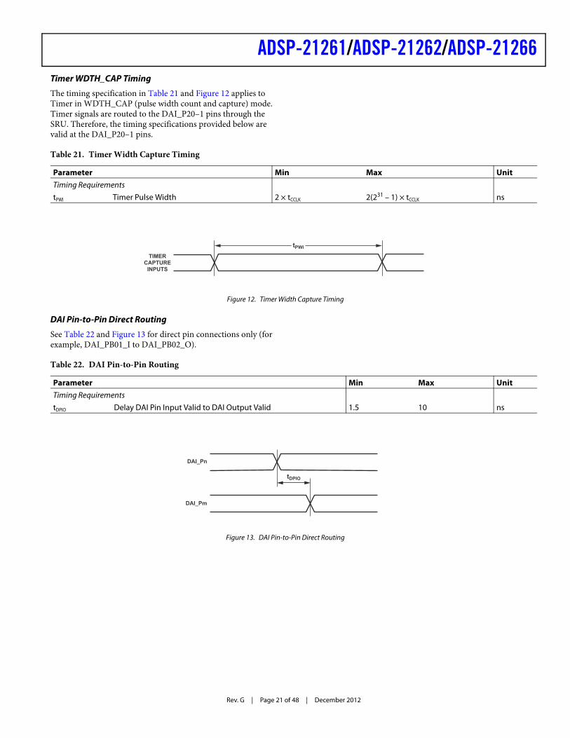
Timer WDTH_CAP Timing
The timing specification in Table 21 and Figure 12 applies to Timer in WDTH_CAP (pulse width count and capture) mode. Timer signals are routed to the DAI_P20–1 pins through the SRU. Therefore, the timing specifications provided below are valid at the DAI_P20–1 pins.
DAI Pin-to-Pin Direct Routing
See Table 22 and Figure 13 for direct pin connections only (for example, DAI_PB01_I to DAI_PB02_O).
Table 21. Timer Width Capture Timing
Parameter Min Max Unit
Timing Requirements
tPWI Timer Pulse Width 2 × tCCLK 2(231 – 1) × tCCLK ns
Figure 12. Timer Width Capture Timing
TIMERCAPTURE
INPUTS
tPWI
Table 22. DAI Pin-to-Pin Routing
Parameter Min Max Unit
Timing Requirements
tDPIO Delay DAI Pin Input Valid to DAI Output Valid 1.5 10 ns
Figure 13. DAI Pin-to-Pin Direct Routing
DAI_Pn
DAI_Pm
tDPIO
Rev. G | Page 22 of 48 | December 2012
ADSP-21261/ADSP-21262/ADSP-21266Precision Clock Generator (Direct Pin Routing)
The timing in Table 23 and Figure 14 is valid only when the SRU is configured such that the precision clock generator (PCG) takes its inputs directly from the DAI pins (via pin buf-fers) and sends its outputs directly to the DAI pins. For the
other cases where the PCG’s inputs and outputs are not directly routed to/from DAI pins (via pin buffers), there is no timing data available. All timing parameters and switching characteris-tics apply to external DAI pins (DAI_P07–DAI_P20).
Table 23. Precision Clock Generator (Direct Pin Routing)
Parameter Min Max Unit
Timing Requirements
tPCGIW Input Clock Pulse Width 20 ns
tSTRIG PCG Trigger Setup Before Falling Edge of PCG Input Clock 2 ns
tHTRIG PCG Trigger Hold After Falling Edge of PCG Input Clock 2 ns
Switching Characteristics
tDPCGIO PCG Output Clock and Frame Sync Active Edge Delay After PCG Input Clock Falling Edge 2.5 10 ns
tDTRIG PCG Output Clock and Frame Sync Delay After PCG Trigger 2.5 + 2.5 × tPCGOW 10 + 2.5 × tPCGOW ns
tPCGOW Output Clock Pulse Width 40 ns
Figure 14. Precision Clock Generator (Direct Pin Routing)
DAI_PnPCG_TRIGx_I
DAI_PmPCG_EXTx_I
(CLKIN)
DAI_PyPCK_CLKx_O
DAI_PzPCG_FSx_O
tDTRIG
tDPCGIO
tSTRIG tHTRIG
tPCGOWtDPCGIO
tPCGIW
ADSP-21261/ADSP-21262/ADSP-21266
Rev. G | Page 23 of 48 | December 2012
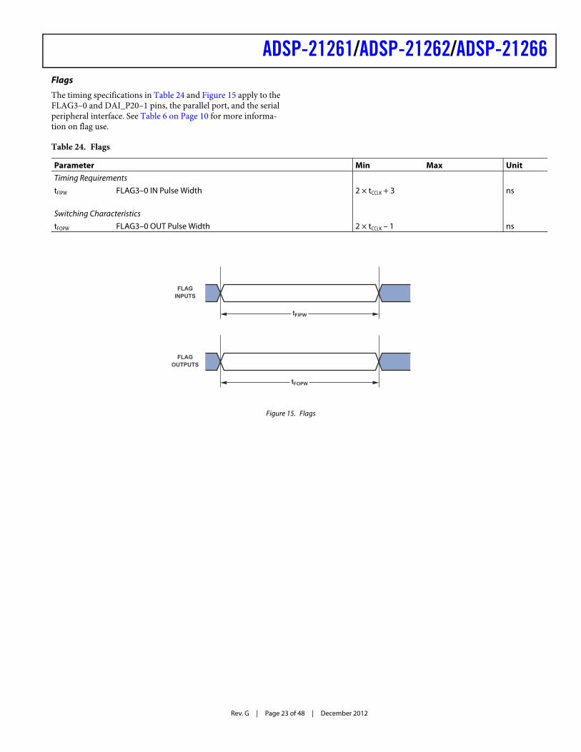
Flags
The timing specifications in Table 24 and Figure 15 apply to the FLAG3–0 and DAI_P20–1 pins, the parallel port, and the serial peripheral interface. See Table 6 on Page 10 for more informa-tion on flag use.
Table 24. Flags
Parameter Min Max Unit
Timing Requirements
tFIPW FLAG3–0 IN Pulse Width 2 × tCCLK + 3 ns
Switching Characteristics
tFOPW FLAG3–0 OUT Pulse Width 2 × tCCLK – 1 ns
Figure 15. Flags
FLAGINPUTS
FLAGOUTPUTS
tFOPW
tFIPW

Rev. G | Page 24 of 48 | December 2012
ADSP-21261/ADSP-21262/ADSP-21266Memory Read—Parallel Port
The specifications in Table 25, Table 26, Figure 16, and Figure 17 are for asynchronous interfacing to memories (and memory-mapped peripherals) when the ADSP-2126x is access-ing external memory space.
Table 25. 8-Bit Memory Read Cycle
Parameter Min Max Unit
Timing Requirements
tDRS Address/Data 7–0 Setup Before RD High 3.3 ns
tDRH Address/Data 7–0 Hold After RD High 0 ns
tDAD Address 15–8 to Data Valid D + 0.5 × tCCLK – 3.5 ns
Switching Characteristics
tALEW ALE Pulse Width 2 × tCCLK – 2 ns
tALERW ALE Deasserted to Read/Write Asserted 1 × tCCLK – 0.5 ns
tADAS1 Address/Data 15–0 Setup Before ALE Deasserted 2.5 × tCCLK – 2.0 ns
tADAH1 Address/Data 15–0 Hold After ALE Deasserted 0.5 × tCCLK – 0.8 ns
tALEHZ1 ALE Deasserted to Address/Data7–0 in High-Z 0.5 × tCCLK – 0.8 0.5 × tCCLK + 2.0 ns
tRW RD Pulse Width D – 2 ns
tADRH Address/Data 15–8 Hold After RD High 0.5 × tCCLK – 1 + H ns
D = (The value set by the PPDUR Bits (5–1) in the PPCTL register) × tCCLK H = tCCLK (if a hold cycle is specified, else H = 0)
1 On reset, ALE is an active high cycle. However, it can be reconfigured by software to be active low.
Figure 16. 8-Bit Memory Read Cycle
AD15-8
ALE
RD
WR
AD7-0
VALID ADDRESS
VALID ADDRESS
tALEW tALERW tRW
tALEHZtADAHtADAS tADRH
tDRHtDRS
VALID ADDRESS
tDAD
VALID DATA

ADSP-21261/ADSP-21262/ADSP-21266
Rev. G | Page 25 of 48 | December 2012
Table 26. 16-Bit Memory Read Cycle
Parameter Min Max Unit
Timing Requirements
tDRS Address/Data 15–0 Setup Before RD high 3.3 ns
tDRH Address/Data 15–0 Hold After RD high 0 ns
Switching Characteristics ns
tALEW ALE Pulse Width 2 × tCCLK – 2 ns
tALERW ALE Deasserted to Read/Write Asserted 1 × tCCLK – 0.5 ns
tADAS1 Address/Data 15–0 Setup Before ALE Deasserted 2.5 × tCCLK – 2.0 ns
tADAH1 Address/Data 15–0 Hold After ALE Deaserted 0.5 × tCCLK – 0.8 ns
tALEHZ1 ALE Deasserted to Address/Data 15–0 in High-Z 0.5 × tCCLK – 0.8 0.5 × tCCLK + 2.0 ns
tRW RD Pulse Width D – 2 ns
D = (The value set by the PPDUR Bits (5–1) in the PPCTL register) × tCCLK H = tCCLK (if a hold cycle is specified, else H = 0)
1 On reset, ALE is an active high cycle. However, it can be reconfigured by software to be active low.
Figure 17. 16-Bit Memory Read Cycle
AD15-0
ALE
RD
WR
VALID ADDRESS
tALEW tALERW tRW
tALEHZtADAHtADAS tDRHtDRS
VALID ADDRESS

Rev. G | Page 26 of 48 | December 2012
ADSP-21261/ADSP-21262/ADSP-21266Memory Write—Parallel Port
Use the specifications in Table 27, Table 28, Figure 18, and Figure 19 for asynchronous interfacing to memories (and memory-mapped peripherals) when the ADSP-2126x is access-ing external memory space.
Table 27. 8-Bit Memory Write Cycle
Parameter Min Max Unit
Switching Characteristics
tALEW ALE Pulse Width 2 × tCCLK – 2 ns
tALERW ALE Deasserted to Read/Write Asserted 1 × tCCLK – 0.5 ns
tADAS1 Address/Data 15–0 Setup Before ALE Deasserted 2.5 × tCCLK – 2.0 ns
tADAH1 Address/Data 15–0 Hold After ALE Deasserted 0.5 × tCCLK – 0.8 ns
tWW WR Pulse Width D – 2 ns
tADWL Address/Data 15–8 to WR Low 0.5 × tCCLK – 1.5 ns
tADWH Address/Data 15–8 Hold After WR High 0.5 × tCCLK – 1 + H ns
tALEHZ ALE Deasserted to Address/Data 15–0 in High-Z 0.5 × tCCLK – 0.8 0.5 × tCCLK + 2.0 ns
tDWS Address/Data 7–0 Setup Before WR High D ns
tDWH Address/Data 7–0 Hold After WR High 0.5 × tCCLK – 1.5 + H ns
tDAWH Address/Data to WR High D ns
D = (The value set by the PPDUR Bits (5–1) in the PPCTL register) × tCCLK H = tCCLK (if a hold cycle is specified, else H = 0)
1 On reset, ALE is an active high cycle. However, it can be reconfigured by software to be active low.
Figure 18. 8-Bit Memory Write Cycle
AD15-8
ALE
WR
RD
AD7-0
VALID ADDRESS
VALID ADDRESS
tALEW tALERW tWW
tALEHZtADAHtADAS
tADWH
tDWHtDWS
VALID ADDRESS
tADWL
VALID DATA
tDAWH

ADSP-21261/ADSP-21262/ADSP-21266
Rev. G | Page 27 of 48 | December 2012
Table 28. 16-Bit Memory Write Cycle
Parameter Min Max Unit
Switching Characteristics
tALEW ALE Pulse Width 2 × tCCLK – 2 ns
tALERW ALE Deasserted to Read/Write Asserted 1 × tCCLK – 0.5 ns
tADAS1 Address/Data 15–0 Setup Before ALE Deasserted 2.5 × tCCLK – 2.0 ns
tADAH1 Address/Data 15–0 Hold After ALE Deasserted 0.5 × tCCLK – 0.8 ns
tWW WR Pulse Width D – 2 ns
tALEHZ1 ALE Deasserted to Address/Data 15–0 in High-Z 0.5 × tCCLK – 0.8 0.5 × tCCLK + 2.0 ns
tDWS Address/Data 15–0 Setup Before WR High D ns
tDWH Address/Data 15–0 Hold After WR High 0.5 × tCCLK – 1.5 + H ns
D = (The value set by the PPDUR Bits (5–1) in the PPCTL register) × tCCLK H = tCCLK (if a hold cycle is specified, else H = 0)
1 On reset, ALE is an active high cycle. However, it can be reconfigured by software to be active low.
Figure 19. 16-Bit Memory Write Cycle
AD15-0
ALE
WR
RD
VALID ADDRESS
tALEW tALERW tWW
tALEHZtADAHtADAS tDWHtDWS
VALID DATA

Rev. G | Page 28 of 48 | December 2012
ADSP-21261/ADSP-21262/ADSP-21266Serial Ports
To determine whether communication is possible between two devices at a given clock speed, the specifications in Table 29, Table 30, Table 31, Table 32, Figure 20, Figure 21, and Figure 22 must be confirmed: 1) frame sync delay and frame sync setup and hold; 2) data delay and data setup and hold; and 3) SCLK width.
Serial port signals (SCLK, FS, DxA,/DxB) are routed to the DAI_P20–1 pins using the SRU. Therefore, the timing specifica-tions provided below are valid at the DAI_P20–1 pins.
Table 29. Serial Ports—External Clock
Parameter Min Max Unit
Timing Requirements
tSFSE FS Setup Before SCLK (Externally Generated FS in Either Transmit or Receive Mode)1 2.5 ns
tHFSE FS Hold After SCLK (Externally Generated FS in Either Transmit or Receive Mode)1 2.5 ns
tSDRE Receive Data Setup Before Receive SCLK1 2.5 ns
tHDRE Receive Data Hold After SCLK1 2.5 ns
tSCLKW SCLK Width 7 ns
tSCLK SCLK Period 20 ns
Switching Characteristics
tDFSE FS Delay After SCLK (Internally Generated FS in Either Transmit or Receive Mode)2 7 ns
tHOFSE FS Hold After SCLK (Internally Generated FS in Either Transmit or Receive Mode)2 2 ns
tDDTE Transmit Data Delay After Transmit SCLK2 7 ns
tHDTE Transmit Data Hold After Transmit SCLK2 2 ns1 Referenced to sample edge.2 Referenced to drive edge.
Table 30. Serial Ports—Internal Clock
Parameter Min Max Unit
Timing Requirements
tSFSI FS Setup Before SCLK (Externally Generated FS in Either Transmit or Receive Mode)1 6 ns
tHFSI FS Hold After SCLK (Externally Generated FS in Either Transmit or Receive Mode)1 1.5 ns
tSDRI Receive Data Setup Before SCLK1 6 ns
tHDRI Receive Data Hold After SCLK1 1.5 ns
Switching Characteristics
tDFSI FS Delay After SCLK (Internally Generated FS in Transmit Mode)2 3 ns
tHOFSI FS Hold After SCLK (Internally Generated FS in Transmit Mode)2 –1.0 ns
tDFSI FS Delay After SCLK (Internally Generated FS in Receive Mode)2 3 ns
tHOFSI FS Hold After SCLK (Internally Generated FS in Receive Mode)2 –1.0 ns
tDDTI Transmit Data Delay After SCLK2 3 ns
tHDTI Transmit Data Hold After SCLK2 –1.0 ns
tSCLKIW Transmit or Receive SCLK Width 0.5tSCLK – 2 0.5tSCLK + 2 ns1 Referenced to the sample edge.2 Referenced to drive edge.

ADSP-21261/ADSP-21262/ADSP-21266
Rev. G | Page 29 of 48 | December 2012
Figure 20. Serial Ports
DRIVE EDGE SAMPLE EDGE
DAI_P20–1(DATA
CHANNEL A/B)
DAI_P20–1(FS)
DAI_P20–1(SCLK)
tHOFSI tHFSI
tHDRI
DATA RECEIVE—INTERNAL CLOCK
DRIVE EDGE SAMPLE EDGE
DAI_P20–1(DATA
CHANNEL A/B)
DAI_P20–1(FS)
DAI_P20–1(SCLK)
tHFSI
tDDTI
DATA TRANSMIT—INTERNAL CLOCK
DRIVE EDGE SAMPLE EDGE
DAI_P20–1(DATA
CHANNEL A/B)
DAI_P20–1(FS)
DAI_P20–1(SCLK)
tHOFSEtHOFSI
tHDTI
tHFSE
tHDTE
tDDTE
DATA TRANSMIT—EXTERNAL CLOCK
DRIVE EDGE SAMPLE EDGE
DAI_P20–1(DATA
CHANNEL A/B)
DAI_P20–1(FS)
DAI_P20–1(SCLK)
tHOFSE tHFSE
tHDRE
DATA RECEIVE—EXTERNAL CLOCK
tSCLKIW
tDFSI
tSFSI
tSDRI
tSCLKW
tDFSE
tSFSE
tSDRE
tDFSE
tSFSEtSFSI
tDFSI
tSCLKIW tSCLKW

Rev. G | Page 30 of 48 | December 2012
ADSP-21261/ADSP-21262/ADSP-21266Table 31. Serial Ports—Enable and Three-State
Parameter Min Max Unit
Switching Characteristics
tDDTEN Data Enable from External Transmit SCLK1 2 ns
tDDTTE Data Disable from External Transmit SCLK1 7 ns
tDDTIN Data Enable from Internal Transmit SCLK1 –1 ns 1 Referenced to drive edge.
Figure 21. Enable and Three-State
DRIVE EDGE
DRIVE EDGE
DRIVE EDGE
tDDTIN
tDDTEN tDDTTE
DAI_P20–1(SCLK, INT)
DAI_P20–1(DATA
CHANNEL A/B)
DAI_P20–1(SCLK, EXT)
DAI_P20–1(DATA
CHANNEL A/B)

ADSP-21261/ADSP-21262/ADSP-21266
Rev. G | Page 31 of 48 | December 2012
Table 32. Serial Ports—External Late Frame Sync
Parameter Min Max Unit
Switching Characteristics
tDDTLFSE Data Delay from Late External Transmit FS or External Receive FS with MCE = 1, MFD = 01 7 ns
tDDTENFS Data Enable for MCE = 1, MFD = 01 0.5 ns1 The tDDTLFSE and tDDTENFS parameters apply to left-justified sample pair mode as well as DSP serial mode, and MCE = 1, MFD = 0.
Figure 22. External Late Frame Sync1
1 This figure reflects changes made to support left-justified sample pair mode.
DRIVE SAMPLE
EXTERNAL RECEIVE FS WITH MCE = 1, MFD = 0
2ND BIT
DAI_P20–1(SCLK)
DAI_P20–1(FS)
DAI_P20–1(DATA CHANNEL
A/B)1ST BIT
DRIVE
tDDTE/I
tHDTE/I
tDDTLFSE
tDDTENFS
tSFSE/I
DRIVE SAMPLE
LATE EXTERNAL TRANSMIT FS
2ND BIT
DAI_P20–1(SCLK)
DAI_P20–1(FS)
DAI_P20–1(DATA CHANNEL
A/B)1ST BIT
DRIVE
tDDTE/I
tHDTE/I
tDDTLFSE
tDDTENFS
tSFSE/I
tHFSE/I
tHFSE/I

Rev. G | Page 32 of 48 | December 2012
ADSP-21261/ADSP-21262/ADSP-21266Input Data Port (IDP)
The timing requirements for the IDP are given in Table 33 and Figure 23. IDP Signals (SCLK, FS, SDATA) are routed to the DAI_P20–1 pins using the SRU. Therefore, the timing specifica-tions provided below are valid at the DAI_P20–1 pins.
Table 33. Input Data Port (IDP)
Parameter Min Max Unit
Timing Requirements
tSISFS FS Setup Before SCLK Rising Edge1 2.5 ns
tSIHFS FS Hold After SCLK Rising Edge1 2.5 ns
tSISD SDATA Setup Before SCLK Rising Edge1 2.5 ns
tSIHD SDATA Hold After SCLK Rising Edge1 2.5 ns
tIDPCLKW Clock Width 7 ns
tIDPCLK Clock Period 20 ns 1 DATA, SCLK, FS can come from any of the DAI pins. SCLK and FS can also come via the precision clock generators (PCG) or SPORTs. PCG input can be either CLKIN or
any of the DAI pins.
Figure 23. Input Data Port (IDP)
DAI_P20–1(SCLK)
SAMPLE EDGE
DAI_P20–1(FS)
DAI_P20–1(SDATA)
tIDPCLK
tIDPCLKW
tSISFS tSIHFS
tSIHDtSISD

ADSP-21261/ADSP-21262/ADSP-21266
Rev. G | Page 33 of 48 | December 2012
Parallel Data Acquisition Port (PDAP)
The timing requirements for the PDAP are provided in Table 34 and Figure 24. PDAP is the parallel mode operation of Channel 0 of the IDP. For details on the operation of the IDP, see the IDP chapter of the ADSP-2126x Peripherals Manual.
Note that the most significant 16 bits of external PDAP data can be provided through either the parallel port AD15–0 or the DAI_P20–5 pins. The remaining four bits can only be sourced through DAI_P4–1. The timing below is valid at the DAI_P20–1 pins or at the AD15–0 pins.
Table 34. Parallel Data Acquisition Port (PDAP)
Parameter Min Max Unit
Timing Requirements
tSPHOLD PDAP_HOLD Setup Before PDAP_CLK Sample Edge1 2.5 ns
tHPHOLD PDAP_HOLD Hold After PDAP_CLK Sample Edge1 2.5 ns
tPDSD PDAP_DAT Setup Before SCLK PDAP_CLK Sample Edge1 2.5 ns
tPDHD PDAP_DAT Hold After SCLK PDAP_CLK Sample Edge1 2.5 ns
tPDCLKW Clock Width 7 ns
tPDCLK Clock Period 20 ns
Switching Characteristics
tPDHLDD Delay of PDAP Strobe After Last PDAP_CLK Capture Edge for a Word 2 × tCCLK ns
tPDSTRB PDAP Strobe Pulse Width 1 × tCCLK – 1 ns 1 Source pins of DATA are ADDR7–0, DATA7–0, or DAI pins. Source pins for SCLK and FS are: 1) DAI pins, 2) CLKIN through PCG, or 3) DAI pins through PCG.
Figure 24. Parallel Data Acquisition Port (PDAP)
DAI_P20–1(PDAP_CLK)
SAMPLE EDGE
DAI_P20–1(PDAP_HOLD)
DAI_P20–1(PDAP_STROBE)
tPDSTRBtPDHLDD
tPDHDtPDSD
tSPHOLD tHPHOLD
tPDCLK
tPDCLKW
DAI_P20–1/ADDR23–4
(PDAP_DATA)
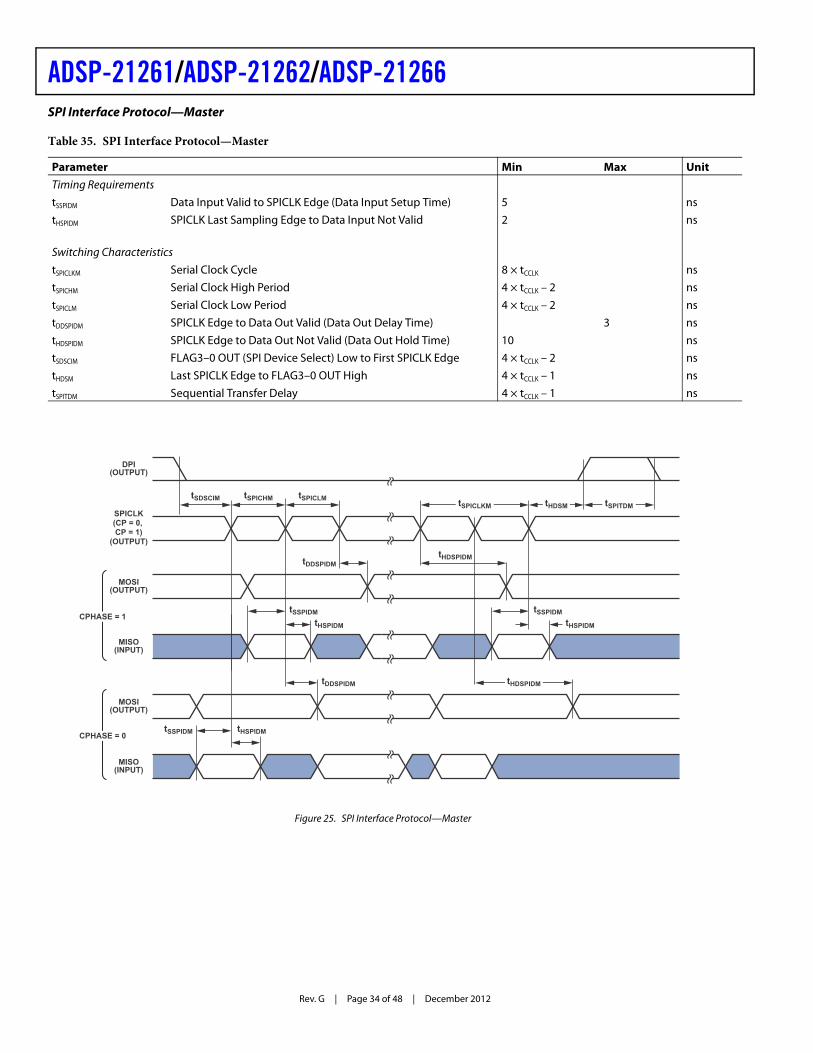
Rev. G | Page 34 of 48 | December 2012
ADSP-21261/ADSP-21262/ADSP-21266SPI Interface Protocol—Master
Table 35. SPI Interface Protocol—Master
Parameter Min Max Unit
Timing Requirements
tSSPIDM Data Input Valid to SPICLK Edge (Data Input Setup Time) 5 ns
tHSPIDM SPICLK Last Sampling Edge to Data Input Not Valid 2 ns
Switching Characteristics
tSPICLKM Serial Clock Cycle 8 × tCCLK ns
tSPICHM Serial Clock High Period 4 × tCCLK – 2 ns
tSPICLM Serial Clock Low Period 4 × tCCLK – 2 ns
tDDSPIDM SPICLK Edge to Data Out Valid (Data Out Delay Time) 3 ns
tHDSPIDM SPICLK Edge to Data Out Not Valid (Data Out Hold Time) 10 ns
tSDSCIM FLAG3–0 OUT (SPI Device Select) Low to First SPICLK Edge 4 × tCCLK – 2 ns
tHDSM Last SPICLK Edge to FLAG3–0 OUT High 4 × tCCLK – 1 ns
tSPITDM Sequential Transfer Delay 4 × tCCLK – 1 ns
Figure 25. SPI Interface Protocol—Master
tSPICHMtSDSCIM tSPICLM tSPICLKM tHDSM tSPITDM
tDDSPIDM
tHSPIDMtSSPIDM
DPI(OUTPUT)
MOSI(OUTPUT)
MISO(INPUT)
MOSI(OUTPUT)
MISO(INPUT)
CPHASE = 1
CPHASE = 0
tHDSPIDM
tHSPIDMtHSPIDM
tSSPIDM tSSPIDM
tDDSPIDM
tHDSPIDM
SPICLK(CP = 0, CP = 1)
(OUTPUT)
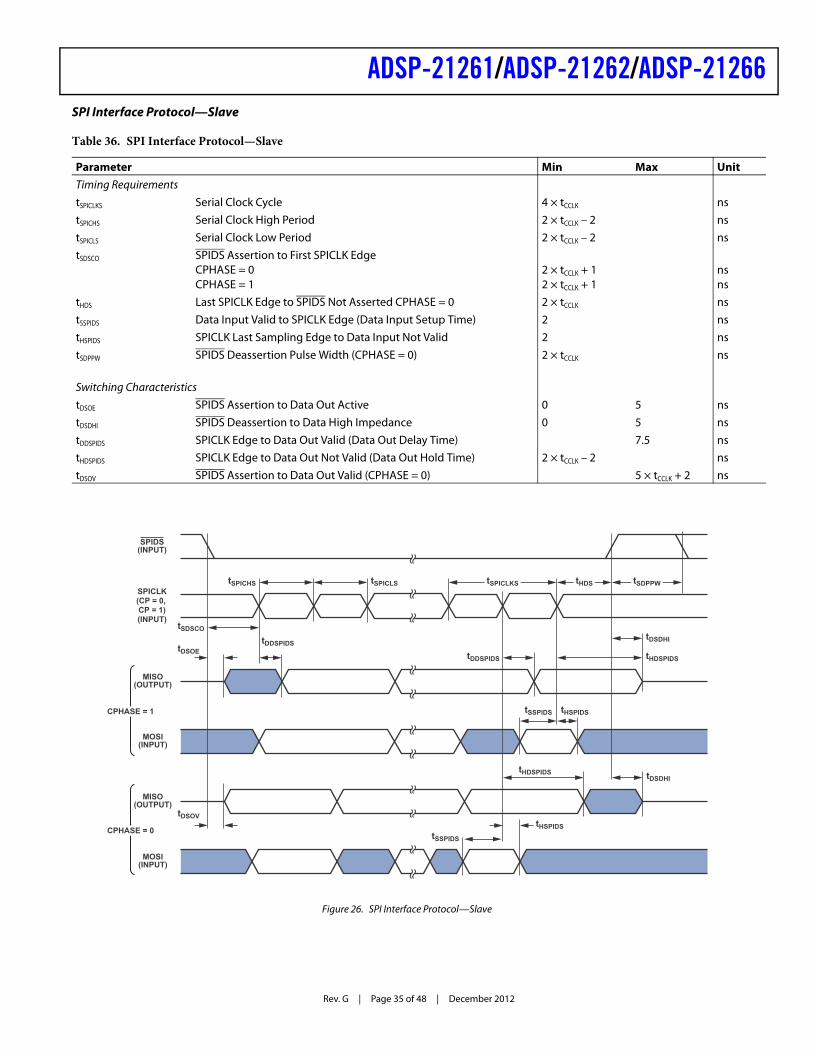
ADSP-21261/ADSP-21262/ADSP-21266
Rev. G | Page 35 of 48 | December 2012
SPI Interface Protocol—Slave
Table 36. SPI Interface Protocol—Slave
Parameter Min Max Unit
Timing Requirements
tSPICLKS Serial Clock Cycle 4 × tCCLK ns
tSPICHS Serial Clock High Period 2 × tCCLK – 2 ns
tSPICLS Serial Clock Low Period 2 × tCCLK – 2 ns
tSDSCO SPIDS Assertion to First SPICLK EdgeCPHASE = 0CPHASE = 1
2 × tCCLK + 12 × tCCLK + 1
nsns
tHDS Last SPICLK Edge to SPIDS Not Asserted CPHASE = 0 2 × tCCLK ns
tSSPIDS Data Input Valid to SPICLK Edge (Data Input Setup Time) 2 ns
tHSPIDS SPICLK Last Sampling Edge to Data Input Not Valid 2 ns
tSDPPW SPIDS Deassertion Pulse Width (CPHASE = 0) 2 × tCCLK ns
Switching Characteristics
tDSOE SPIDS Assertion to Data Out Active 0 5 ns
tDSDHI SPIDS Deassertion to Data High Impedance 0 5 ns
tDDSPIDS SPICLK Edge to Data Out Valid (Data Out Delay Time) 7.5 ns
tHDSPIDS SPICLK Edge to Data Out Not Valid (Data Out Hold Time) 2 × tCCLK – 2 ns
tDSOV SPIDS Assertion to Data Out Valid (CPHASE = 0) 5 × tCCLK + 2 ns
Figure 26. SPI Interface Protocol—Slave
tSPICHS tSPICLS tSPICLKS tHDS tSDPPW
tSDSCO
tDSOEtDDSPIDS
tDDSPIDS
tDSDHI
tHDSPIDS
tHSPIDStSSPIDS
tDSDHI
tDSOVtHSPIDS
tHDSPIDS
SPIDS(INPUT)
MISO(OUTPUT)
MOSI(INPUT)
MISO(OUTPUT)
MOSI(INPUT)
CPHASE = 1
CPHASE = 0
SPICLK(CP = 0, CP = 1)(INPUT)
tSSPIDS
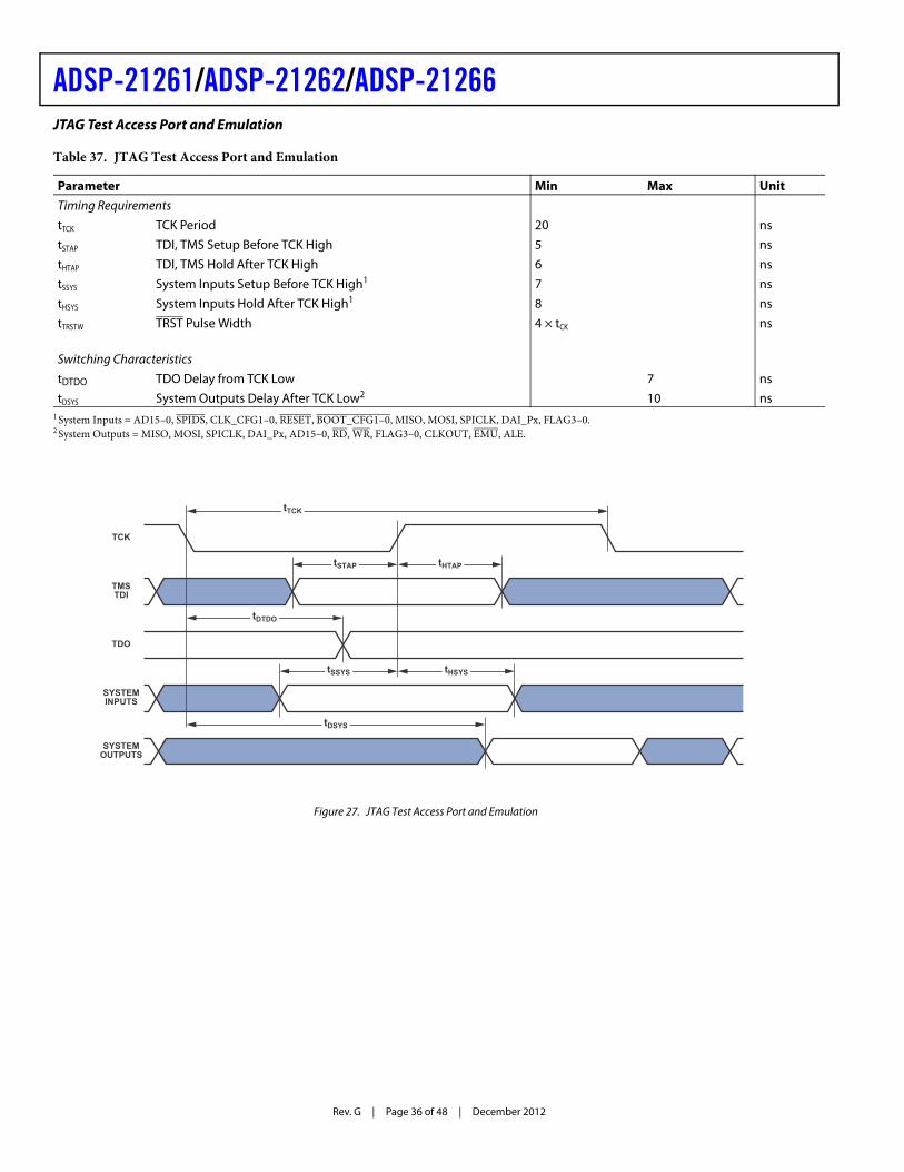
Rev. G | Page 36 of 48 | December 2012
ADSP-21261/ADSP-21262/ADSP-21266JTAG Test Access Port and Emulation
Table 37. JTAG Test Access Port and Emulation
Parameter Min Max Unit
Timing Requirements
tTCK TCK Period 20 ns
tSTAP TDI, TMS Setup Before TCK High 5 ns
tHTAP TDI, TMS Hold After TCK High 6 ns
tSSYS System Inputs Setup Before TCK High1 7 ns
tHSYS System Inputs Hold After TCK High1 8 ns
tTRSTW TRST Pulse Width 4 × tCK ns
Switching Characteristics
tDTDO TDO Delay from TCK Low 7 ns
tDSYS System Outputs Delay After TCK Low2 10 ns1 System Inputs = AD15–0, SPIDS, CLK_CFG1–0, RESET, BOOT_CFG1–0, MISO, MOSI, SPICLK, DAI_Px, FLAG3–0.2 System Outputs = MISO, MOSI, SPICLK, DAI_Px, AD15–0, RD, WR, FLAG3–0, CLKOUT, EMU, ALE.
Figure 27. JTAG Test Access Port and Emulation
TCK
TMSTDI
TDO
SYSTEMINPUTS
SYSTEMOUTPUTS
tTCK
tSTAP tHTAP
tDTDO
tSSYS tHSYS
tDSYS

ADSP-21261/ADSP-21262/ADSP-21266
Rev. G | Page 37 of 48 | December 2012
OUTPUT DRIVE CURRENTS
Figure 28 shows typical I-V characteristics for the output driv-ers of the ADSP-2126x. The curves represent the current drive capability of the output drivers as a function of output voltage.
TEST CONDITIONS
The ac signal specifications (timing parameters) appear in Table 16 on Page 18 through Table 37 on Page 36. These include output disable time, output enable time, and capacitive loading. Timing is measured on signals when they cross the 1.5 V level as described in Figure 30. All delays (in nanoseconds) are mea-sured between the point that the first signal reaches 1.5 V and the point that the second signal reaches 1.5 V.
CAPACITIVE LOADING
Output delays and holds are based on standard capacitive loads: 30 pF on all pins (see Figure 29). Figure 32 shows graphically how output delays and holds vary with load capacitance (note that this graph or derating does not apply to output disable delays). The graphs of Figure 31, Figure 32, and Figure 33 may not be linear outside the ranges shown for Typical Output Delay vs. Load Capacitance and Typical Output Rise Time (20% to 80%, V = Min) vs. Load Capacitance.
Figure 28. Typical Drive
Figure 29. Equivalent Device Loading for AC Measurements (Includes All Fixtures)
Figure 30. Voltage Reference Levels for AC Measurements
SWEEP (VDDEXT) VOLTAGE (V)
–20
0 3.50.5 1 1.5 2 2.5 3
0
–40
–30
20
40
–10
SO
UR
CE
(VD
DE
XT
)C
UR
RE
NT
(mA
)
VOL
3.11V, 125°C
3.3V, 25°C
3.47V, –45°C
VOH30
10
3.11V, 125°C
3.3V, 25°C
3.47V, –45°C
1.5V
30pF
TOOUTPUT
PIN
50�
INPUTOR
OUTPUT 1.5V 1.5V
Figure 31. Typical Output Rise Time (20% to 80%, VDDEXT = Max)
Figure 32. Typical Output Rise/Fall Time (20% to 80%, VDDEXT = Min)
LOAD CAPACITANCE (pF)
8
00 100 250
12
4
2
10
6
RIS
EA
ND
FA
LL
TIM
ES
(ns)
20015050
FALLy = 0.0467x + 1.6323
y = 0.045x + 1.524
RISE
LOAD CAPACITANCE (pF)
12
0 50 100 150 200 250
10
8
6
4
RIS
EA
ND
FA
LL
TIM
ES
(ns)
2
0
RISE
FALLy = 0.049x + 1.5105
y = 0.0482x + 1.4604
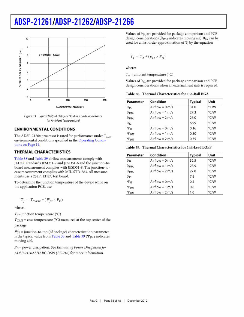
Rev. G | Page 38 of 48 | December 2012
ADSP-21261/ADSP-21262/ADSP-21266
ENVIRONMENTAL CONDITIONS
The ADSP-2126x processor is rated for performance under TAMB environmental conditions specified in the Operating Condi-tions on Page 14.
THERMAL CHARACTERISTICS
Table 38 and Table 39 airflow measurements comply with JEDEC standards JESD51-2 and JESD51-6 and the junction-to-board measurement complies with JESD51-8. The junction-to-case measurement complies with MIL-STD-883. All measure-ments use a 2S2P JEDEC test board.To determine the junction temperature of the device while on the application PCB, use
where:
TJ = junction temperature (°C)TCASE = case temperature (°C) measured at the top center of the package
JT = junction-to-top (of package) characterization parameter is the typical value from Table 38 and Table 39 (JMT indicates moving air).
PD = power dissipation. See Estimating Power Dissipation for ADSP-21262 SHARC DSPs (EE-216) for more information.
Values of JA are provided for package comparison and PCB design considerations (JMA indicates moving air). JA can be used for a first order approximation of TJ by the equation
where:
TA = ambient temperature C)
Values of JC are provided for package comparison and PCB design considerations when an external heat sink is required.
Figure 33. Typical Output Delay or Hold vs. Load Capacitance (at Ambient Temperature)
LOAD CAPACITANCE (pF)
0 20050 100 150
10
8
OU
TP
UT
DE
LA
YO
RH
OL
D(n
s)
–4
6
0
4
2
–2
y = 0.0488x – 1.5923
TJ TCASE JT PD +=
Table 38. Thermal Characteristics for 136-Ball BGA
Parameter Condition Typical Unit
JA Airflow = 0 m/s 31.0 C/W
JMA Airflow = 1 m/s 27.3 °C/W
JMA Airflow = 2 m/s 26.0 °C/W
JC 6.99 °C/W
JT Airflow = 0 m/s 0.16 °C/W
JMT Airflow = 1 m/s 0.30 °C/W
JMT Airflow = 2 m/s 0.35 °C/W
Table 39. Thermal Characteristics for 144-Lead LQFP
Parameter Condition Typical Unit
JA Airflow = 0 m/s 32.5 °C/W
JMA Airflow = 1 m/s 28.9 °C/W
JMA Airflow = 2 m/s 27.8 °C/W
JC 7.8 °C/W
JT Airflow = 0 m/s 0.5 °C/W
JMT Airflow = 1 m/s 0.8 °C/W
JMT Airflow = 2 m/s 1.0 °C/W
TJ TA JA PD +=

ADSP-21261/ADSP-21262/ADSP-21266
Rev. G | Page 39 of 48 | December 2012
144-LEAD LQFP PIN CONFIGURATIONSTable 40 shows the ADSP-2126x’s pin names and their default function after reset (in parentheses).
Table 40. 144-Lead LQFP Pin Assignments
Pin NameLQFP Pin No. Pin Name
LQFP Pin No. Pin Name
LQFP Pin No. Pin Name
LQFP Pin No.
VDDINT 1 VDDINT 37 VDDEXT 73 GND 109
CLK_CFG0 2 GND 38 GND 74 VDDINT 110
CLK_CFG1 3 RD 39 VDDINT 75 GND 111
BOOT_CFG0 4 ALE 40 GND 76 VDDINT 112
BOOT_CFG1 5 AD15 41 DAI_P10 (SD2B) 77 GND 113
GND 6 AD14 42 DAI_P11 (SD3A) 78 VDDINT 114
VDDEXT 7 AD13 43 DAI_P12 (SD3B) 79 GND 115
GND 8 GND 44 DAI_P13 (SCLK23) 80 VDDEXT 116
VDDINT 9 VDDEXT 45 DAI_P14 (SFS23) 81 GND 117
GND 10 AD12 46 DAI_P15 (SD4A) 82 VDDINT 118
VDDINT 11 VDDINT 47 VDDINT 83 GND 119
GND 12 GND 48 GND 84 VDDINT 120
VDDINT 13 AD11 49 GND 85 RESET 121
GND 14 AD10 50 DAI_P16 (SD4B) 86 SPIDS 122
FLAG0 15 AD9 51 DAI_P17 (SD5A) 87 GND 123
FLAG1 16 AD8 52 DAI_P18 (SD5B) 88 VDDINT 124
AD7 17 DAI_P1 (SD0A) 53 DAI_P19 (SCLK45) 89 SPICLK 125
GND 18 VDDINT 54 VDDINT 90 MISO 126
VDDINT 19 GND 55 GND 91 MOSI 127
GND 20 DAI_P2 (SD0B) 56 GND 92 GND 128
VDDEXT 21 DAI_P3 (SCLK0) 57 VDDEXT 93 VDDINT 129
GND 22 GND 58 DAI_P20 (SFS45) 94 VDDEXT 130
VDDINT 23 VDDEXT 59 GND 95 AVDD 131
AD6 24 VDDINT 60 VDDINT 96 AVSS 132
AD5 25 GND 61 FLAG2 97 GND 133
AD4 26 DAI_P4 (SFS0) 62 FLAG3 98 RESETOUT 134
VDDINT 27 DAI_P5 (SD1A) 63 VDDINT 99 EMU 135
GND 28 DAI_P6 (SD1B) 64 GND 100 TDO 136
AD3 29 DAI_P7 (SCLK1) 65 VDDINT 101 TDI 137
AD2 30 VDDINT 66 GND 102 TRST 138
VDDEXT 31 GND 67 VDDINT 103 TCK 139
GND 32 VDDINT 68 GND 104 TMS 140
AD1 33 GND 69 VDDINT 105 GND 141
AD0 34 DAI_P8 (SFS1) 70 GND 106 CLKIN 142
WR 35 DAI_P9 (SD2A) 71 VDDINT 107 XTAL 143
VDDINT 36 VDDINT 72 VDDINT 108 VDDEXT 144
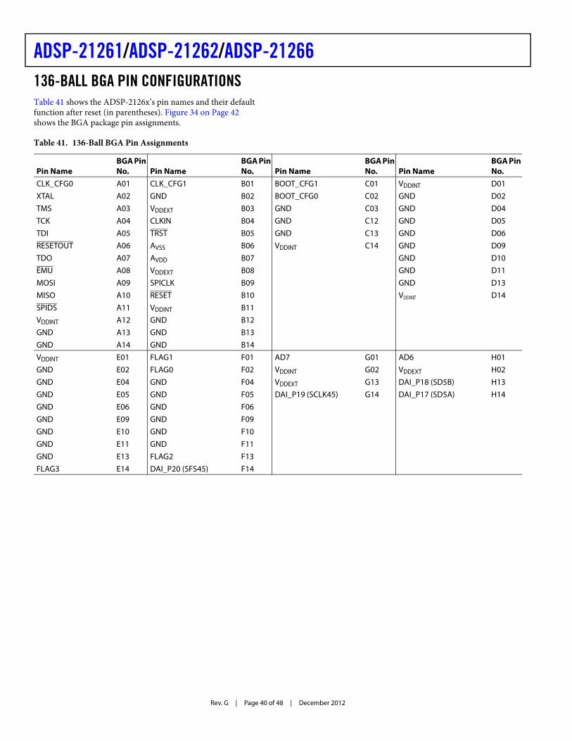
Rev. G | Page 40 of 48 | December 2012
ADSP-21261/ADSP-21262/ADSP-21266136-BALL BGA PIN CONFIGURATIONSTable 41 shows the ADSP-2126x’s pin names and their default function after reset (in parentheses). Figure 34 on Page 42 shows the BGA package pin assignments.
Table 41. 136-Ball BGA Pin Assignments
Pin NameBGA Pin No. Pin Name
BGA Pin No. Pin Name
BGA Pin No. Pin Name
BGA Pin No.
CLK_CFG0 A01 CLK_CFG1 B01 BOOT_CFG1 C01 VDDINT D01
XTAL A02 GND B02 BOOT_CFG0 C02 GND D02
TMS A03 VDDEXT B03 GND C03 GND D04
TCK A04 CLKIN B04 GND C12 GND D05
TDI A05 TRST B05 GND C13 GND D06
RESETOUT A06 AVSS B06 VDDINT C14 GND D09
TDO A07 AVDD B07 GND D10
EMU A08 VDDEXT B08 GND D11
MOSI A09 SPICLK B09 GND D13
MISO A10 RESET B10 VDDINT D14
SPIDS A11 VDDINT B11
VDDINT A12 GND B12
GND A13 GND B13
GND A14 GND B14
VDDINT E01 FLAG1 F01 AD7 G01 AD6 H01
GND E02 FLAG0 F02 VDDINT G02 VDDEXT H02
GND E04 GND F04 VDDEXT G13 DAI_P18 (SD5B) H13
GND E05 GND F05 DAI_P19 (SCLK45) G14 DAI_P17 (SD5A) H14
GND E06 GND F06
GND E09 GND F09
GND E10 GND F10
GND E11 GND F11
GND E13 FLAG2 F13
FLAG3 E14 DAI_P20 (SFS45) F14
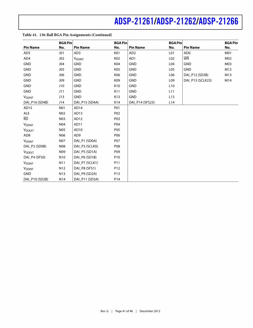
ADSP-21261/ADSP-21262/ADSP-21266
Rev. G | Page 41 of 48 | December 2012
AD5 J01 AD3 K01 AD2 L01 AD0 M01
AD4 J02 VDDINT K02 AD1 L02 WR M02
GND J04 GND K04 GND L04 GND M03
GND J05 GND K05 GND L05 GND M12
GND J06 GND K06 GND L06 DAI_P12 (SD3B) M13
GND J09 GND K09 GND L09 DAI_P13 (SCLK23) M14
GND J10 GND K10 GND L10
GND J11 GND K11 GND L11
VDDINT J13 GND K13 GND L13
DAI_P16 (SD4B) J14 DAI_P15 (SD4A) K14 DAI_P14 (SFS23) L14
AD15 N01 AD14 P01
ALE N02 AD13 P02
RD N03 AD12 P03
VDDINT N04 AD11 P04
VDDEXT N05 AD10 P05
AD8 N06 AD9 P06
VDDINT N07 DAI_P1 (SD0A) P07
DAI_P2 (SD0B) N08 DAI_P3 (SCLK0) P08
VDDEXT N09 DAI_P5 (SD1A) P09
DAI_P4 (SFS0) N10 DAI_P6 (SD1B) P10
VDDINT N11 DAI_P7 (SCLK1) P11
VDDINT N12 DAI_P8 (SFS1) P12
GND N13 DAI_P9 (SD2A) P13
DAI_P10 (SD2B) N14 DAI_P11 (SD3A) P14
Table 41. 136-Ball BGA Pin Assignments (Continued)
Pin NameBGA Pin No. Pin Name
BGA Pin No. Pin Name
BGA Pin No. Pin Name
BGA Pin No.

Rev. G | Page 42 of 48 | December 2012
ADSP-21261/ADSP-21262/ADSP-21266
Figure 34. 136-Ball BGA Pin Assignments (Bottom View, Summary)
AVSS
VDDINT
VDDEXT I/O SIGNALS
AVDDGND
USE THE CENTER BLOCK OF GROUND PINS TO PROVIDETHERMAL PATHWAYS TO YOUR PRINTED
CIRCUIT BOARD’S GROUND PLANE.
KEY
12345678910111214 13
P
N
M
L
K
J
H
G
F
E
D
C
B
A
*

ADSP-21261/ADSP-21262/ADSP-21266
Rev. G | Page 43 of 48 | December 2012
OUTLINE DIMENSIONSThe ADSP-2126x is available in a 144-lead LQFP package and a 136-ball BGA package shown in Figure 35 and Figure 36.
Figure 35. 144-Lead Low Profile Flat Package [LQFP] (ST-144)
Dimensions shown in millimeters
COMPLIANT TO JEDEC STANDARDS MS-026-BFB
0.270.220.17
1
36
3773
72
108144 109
TOP VIEW(PINS DOWN)
0.50BSC
LEAD PITCH
1.60MAX
0.750.600.45
VIEW A
PIN 1
1.451.401.35
0.150.05
0.200.09
0.08 COPLANARITY
VIEW AROTATED 90° CCW
SEATINGPLANE
7°3.5°0°
22.2022.00 SQ21.80
20.2020.00 SQ19.80

Rev. G | Page 44 of 48 | December 2012
ADSP-21261/ADSP-21262/ADSP-21266
SURFACE-MOUNT DESIGN
Table 42 is provided as an aide to PCB design. For industry-standard design recommendations, refer to IPC-7351, Generic Requirements for Surface-Mount Design and Land Pattern Standard.
Figure 36. 136-Ball Chip Scale Package Ball Grid Array [CSP_BGA] (BC-136-1)
Dimensions shown in millimeters
*COMPLIANT WITH JEDEC STANDARDS MO-205-AE WITH EXCEPTION TO BALL DIAMETER.
0.25 MIN
DETAIL A
*0.500.450.40
BALL DIAMETER
0.12 MAXCOPLANARITY
0.80 BSC
10.40BSC SQ
ABCDEFGHJKLM
121314 11 10 8 7 6 3 2 19 5 4
1.311.211.10
A1 CORNERINDEX AREA
1.70 MAX
TOP VIEW
BALL A1INDICATOR
DETAIL A
BOTTOM VIEW
NP
12.1012.00 SQ11.90
SEATINGPLANE
Table 42. BGA_ED Data for Use with Surface-Mount Design
Package Ball Attach Type Solder Mask Opening Ball Pad Size
136-Ball CSP_BGA (BC-136-1) Solder Mask Defined (SMD) 0.4 mm 0.53 mm

ADSP-21261/ADSP-21262/ADSP-21266
Rev. G | Page 45 of 48 | December 2012
AUTOMOTIVE PRODUCTS
The ADSP-21261W and ADSP-21262W are available for auto-motive applications with controlled manufacturing. Note that these special models may have specifications that differ from the general release models. Contact your local ADI account repre-
sentative or authorized ADI product distributor for specific product ordering information. Note that all automotive prod-ucts are RoHS compliant.
ORDERING GUIDE
Analog Devices offers a wide variety of audio algorithms and combinations to run on the ADSP-21266 DSP. For a complete list, visit our website at www.analog.com/SHARC.
Model NotesTemperature Range1
Instruction Rate
On-Chip SRAM ROM Package Description
Package Option
ADSP-21261SKBCZ150 2 0C to +70C 150 MHz 1M bit 3M bit 136-Ball CSP_BGA BC-136-1
ADSP-21261SKSTZ150 2 0C to +70C 150 MHz 1M bit 3M bit 144-Lead LQFP ST-144
ADSP-21262SBBC-150 –40C to +85C 150 MHz 2M bit 4M bit 136-Ball CSP_BGA BC-136-1
ADSP-21262SBBCZ150 2 –40C to +85C 150 MHz 2M bit 4M bit 136-Ball CSP_BGA BC-136-1
ADSP-21262SKBC-200 0C to +70C 200 MHz 2M bit 4M bit 136-Ball CSP_BGA BC-136-1
ADSP-21262SKBCZ200 2 0C to +70C 200 MHz 2M bit 4M bit 136-Ball CSP_BGA BC-136-1
ADSP-21262SKSTZ200 2 0C to +70C 200 MHz 2M bit 4M bit 144-Lead LQFP ST-144
ADSP-21266SKSTZ-1B 2, 3 0C to +70C 150 MHz 2M bit 4M bit 144-Lead LQFP ST-144
ADSP-21266SKSTZ-2B 2, 3 0C to +70C 200 MHz 2M bit 4M bit 144-Lead LQFP ST-144
ADSP-21266SKBCZ-2B 2, 3 0C to +70C 200 MHz 2M bit 4M bit 136-Ball CSP_BGA BC-136-1
ADSP-21266SKSTZ-1C 2, 4 0C to +70C 150 MHz 2M bit 4M bit 144-Lead LQFP ST-144
ADSP-21266SKSTZ-2C 2, 4 0C to +70C 200 MHz 2M bit 4M bit 144-Lead LQFP ST-144
ADSP-21266SKBCZ-2C 2, 4 0C to +70C 200 MHz 2M bit 4M bit 136-Ball CSP_BGA BC-136-1
ADSP-21266SKSTZ-1D 2, 4 0C to +70C 150 MHz 2M bit 4M bit 144-Lead LQFP ST-144
ADSP-21266SKSTZ-2D 2, 4 0C to +70C 200 MHz 2M bit 4M bit 144-Lead LQFP ST-144
ADSP-21266SKBCZ-2D 2, 4 0C to +70C 200 MHz 2M bit 4M bit 136-Ball CSP_BGA BC-136-11 Referenced temperature is ambient temperature.2 Z = RoHS Compliant Part.3 B at end of part number indicates Rev. 0.1 silicon. See Table 3 on Page 4 for multichannel surround sound decoder algorithms in on-chip B ROM.4 C and D at end of part number indicate Rev. 0.2 silicon. See Table 3 on Page 4 for multichannel surround sound decoder algorithms in on-chip C and D ROM.

Rev. G | Page 46 of 48 | December 2012
ADSP-21261/ADSP-21262/ADSP-21266

ADSP-21261/ADSP-21262/ADSP-21266
Rev. G | Page 47 of 48 | December 2012

Rev. G | Page 48 of 48 | December 2012
ADSP-21261/ADSP-21262/ADSP-21266
©2012 Analog Devices, Inc. All rights reserved. Trademarks andregistered trademarks are the property of their respective owners.
D04932-0-12/12(G)


