Seminar DESY Zeuthen 20.01.04 Alexander Oh, CERN
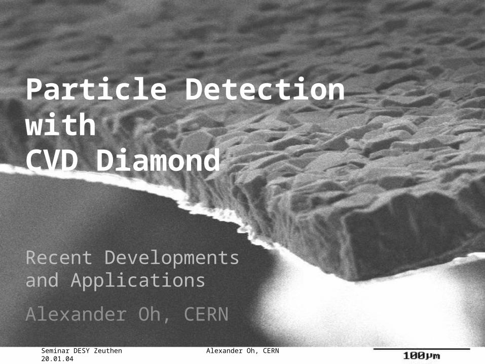
Particle Detection with CVD Diamond
Alexander Oh, CERN
Recent Developments and Applications
Seminar DESY Zeuthen 20.01.04 Alexander Oh, CERN
Outline
• Introduction
• Material Studies
• Particle Detector Prototypes
• Applications in HEP
• Summary
Seminar DESY Zeuthen 20.01.04 Alexander Oh, CERN
Sources• RD42 Collaboration• University Bonn• BaBar, SLAC• CMS, CERN

Seminar DESY Zeuthen 20.01.04 Alexander Oh, CERN
W. Adam1, E. Berdermann2, P. Bergonzo3, W. deBoer21, F. Bogani4, E. Borchi5, A. Brambilla3,M. Bruzzi5, C. Colledani6, J. Conway7, P. D'Angelo8,W. Dabrowski9, P. Delpierre10, W. Dulinski6,J. Doroshenko7, B. van Eijk12, A. Fallou10, P. Fischer20,F. Fizzotti13, C. Furetta8, K.K. Gan14, N. Ghodbane11,E. Grigoriev21, G. Hallewell10, S. Han14, F. Hartjes12,J. Hrubec1, D. Husson6, H. Kagan14;*, J. Kaplon15,R. Kass14, M. Keil20, K.T. Knoepfle16, T. Koeth7,M. Krammer1, A. Logiudice13, R. Lu13, L. Mac Lynne7,C. Manfredotti13, D. Meier15, D. Menichelli5,S. Meuser20, M. Mishina17, L. Moroni8, J. Noomen12,A. Oh15, M. Pernicka1, L. Perera7, R. Potenza22,J.L. Riester6, S. Roe15, A. Rudge15, S. Sala8,M. Sampietro18, S. Schnetzer7, S. Sciortino5, H. Stelzer2,R. Stone7, C. Sutera22, W. Trischuk19, D. Tromson3,C. Tuve22, B. Vincenzo22, P. Weilhammer15,N. Wermes20, M. Wetstein7, W. Zeuner11, M. Zoeller14
1 HEPHY, Vienna, Austria2 GSI, Darmstadt, Germany3 LETI/DEIN/SPE/CEA Saclay, France4 LENS, Florence, Italy5 University of Florence, Italy6 LEPSI, IN2P3/CNRS-ULP, Strasbourg, France7 Rutgers University, Piscataway, U.S.A.8 INFN, Milano, Italy9 UMM, Cracow, Poland10 CPPM, Marseille, France11 II.Inst. f. Exp. Physik, Hamburg, Germany12 NIKHEF, Amsterdam, Netherlands13 University of Torino, Italy14 Ohio State University, Columbus, OH, U.S.A.15 CERN, Geneva, Switzerland16 MPI f. Kernphysik, Heidelberg, Germany17 FNAL, Batavia, IL, U.S.A.18 Polytechnico Milano, Italy19 University of Toronto, Canada20 Universitaet Bonn, Bonn, Germany21 Universitaet Karlsruhe, Karlsruhe, Germany22 University of Roma, Italy* Spokespersons
The RD42 Collaboration: Institutes from HEP, Heavy Ion Physics, Solid State Physics

Seminar DESY Zeuthen 20.01.04 Alexander Oh, CERN
Introduction• Historical Overview
– 1913 Röntgen, Joffé, x-ray detection• Resistivity changes of different materials under x-rays exposure
– 1941 Stetten, Counter experiments with natural diamond• Alpha particle detection with natural diamond
– 1945 van Heerden, Crystal Counters• Wide range of crystal counters investigated, also diamond.
– 1984 Angus & Hayman• Low pressure, metastable growth of diamond and diamond-like phases
– 1994 Tesarek et al.• Performance of a Diamond Tungsten Calorimeter
– “First thermo-luminescence experiment”:
Robert Boyle, 28th Oct 1663, Royal Society, London:“I also brought it to some kind of glimmering light by taking it into bed with me, and holding it a good while upon a
warm part of my naked body”

Seminar DESY Zeuthen 20.01.04 Alexander Oh, CERN
Introduction• Motivation
– LHC and SLHC radiation levels at inner tracking layers O(1015 n cm-2)
– Detectors close to IP or at low rapidity• Vertexdetector• Beam monitoring
• Some advantageous properties of Diamond compared to Silicon :
Seminar DESY Zeuthen 20.01.04 Alexander Oh, CERN
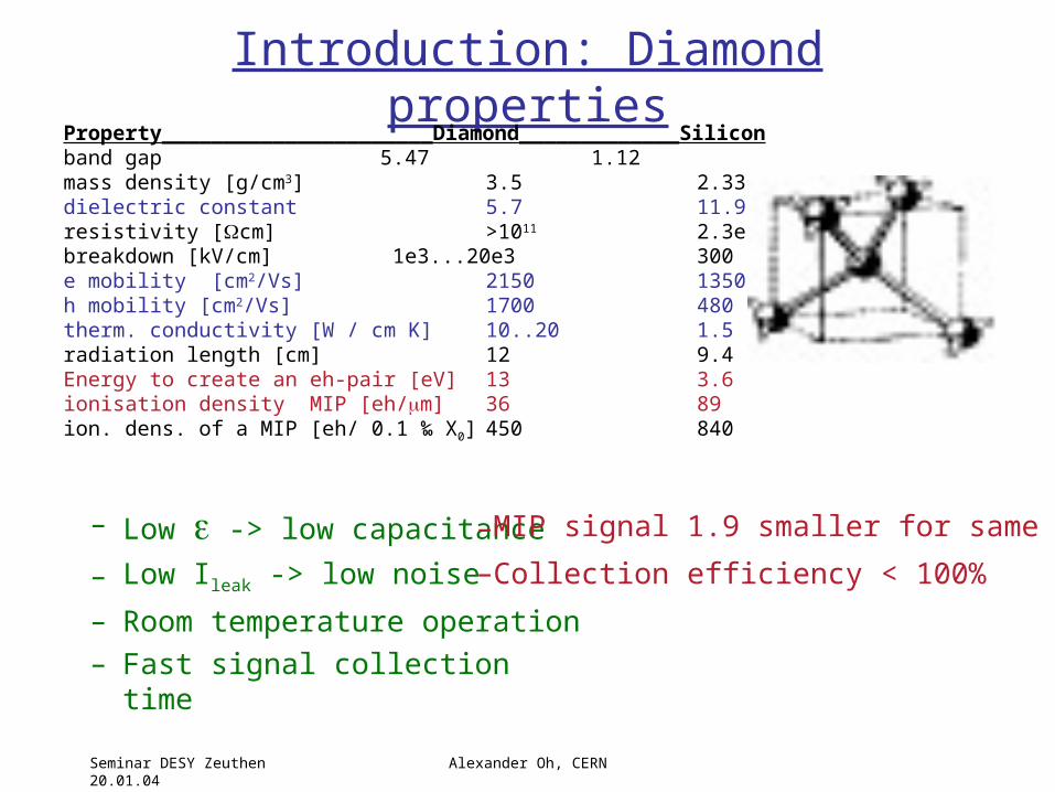
Introduction: Diamond properties
– Low -> low capacitance
– Low Ileak -> low noise
– Room temperature operation– Fast signal collection time
Property______________________Diamond_____________Siliconband gap 5.47 1.12mass density [g/cm3] 3.5 2.33dielectric constant 5.7 11.9resistivity [cm] >1011 2.3e5breakdown [kV/cm] 1e3...20e3 300e mobility [cm2/Vs] 2150 1350h mobility [cm2/Vs] 1700 480therm. conductivity [W / cm K]10..20 1.5radiation length [cm] 12 9.4Energy to create an eh-pair [eV] 13 3.6ionisation density MIP [eh/m] 36 89ion. dens. of a MIP [eh/ 0.1 ‰ X0] 450 840
–MIP signal 1.9 smaller for same X0
–Collection efficiency < 100%
Seminar DESY Zeuthen 20.01.04 Alexander Oh, CERN
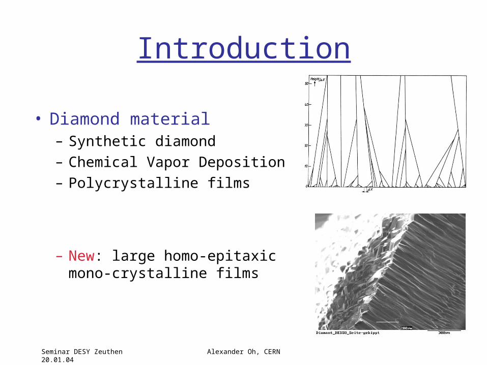
Introduction
• Diamond material– Synthetic diamond– Chemical Vapor Deposition– Polycrystalline films
– New: large homo-epitaxic mono-crystalline films

Seminar DESY Zeuthen 20.01.04 Alexander Oh, CERN
Introduction: CVD process
• CVD: Chemical Vapor Deposition
• Allows deposition of diamond on large areas in arbitrary geometries.
• CVD Diamond is composed of columnar microcrystals.
• Growth speed m / h

Seminar DESY Zeuthen 20.01.04 Alexander Oh, CERN
Introduction• Principle of detector operation
e
h
Substrate-Side
Growth-Side
td collected charge
“collection distance”
= Q / Q0collection efficiency

Seminar DESY Zeuthen 20.01.04 Alexander Oh, CERN
Introduction: Trapping• The charge collection efficiency is for CVDD <100%.
• Free charge carriers are captured at defects in the lattice.
conduction band
valence band
Seminar DESY Zeuthen 20.01.04 Alexander Oh, CERN
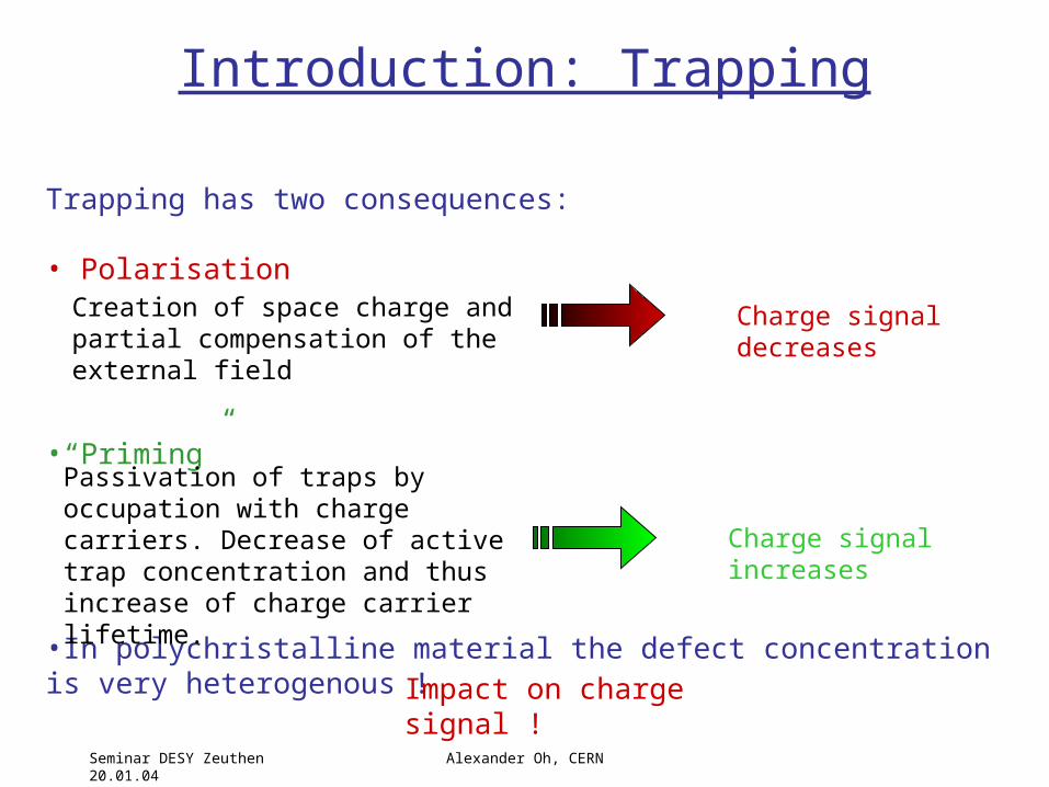
Trapping has two consequences:
• Polarisation
•“Priming”
•In polychristalline material the defect concentration is very heterogenous !
Creation of space charge and partial compensation of the external field
Charge signal decreases
Passivation of traps by occupation with charge carriers. Decrease of active trap concentration and thus increase of charge carrier lifetime.
Charge signal increases
Impact on charge signal !
Introduction: Trapping
Seminar DESY Zeuthen 20.01.04 Alexander Oh, CERN
Material Studies

Seminar DESY Zeuthen 20.01.04 Alexander Oh, CERN
1.0E+00
1.0E+01
1.0E+02
1.0E+03
1.0E+04
1.0E+05
1.0E+06
0 200 400 600 800 1000
Distance [µm]
Concentration [ppmat]
1
1
2
3
300 m
Structure• Scanning Electron Microscopy (SEM)
Pictures show a polycrystalline structure with columnar growth.
• A resolved measurement of Bragg reflexes of single crystallites confirms the growth morphology..
• Secondary Ion Mass Spectroscopy allows to analyze the element concentration as a function of position. A increased concentration of foreign atoms at grain boundaries is found.
H
N
O

Seminar DESY Zeuthen 20.01.04 Alexander Oh, CERN
Characterisation with ionising radiation
• constant ionization density
• measurement of < >Z (x) •Weak polarization
• Bragg ionization density• measurement of (z=S,x) • strong polarization
MIPS, e- (>1,2 MeV), (10 keV)
p (2 MeV), (5,8 MeV)
ElectronsHoles
Z
X• Resolved measurement can be achieved through beam steering or track reconstruction.

Seminar DESY Zeuthen 20.01.04 Alexander Oh, CERN
• Characterisation with 90Sr-source, E,max = 2.28 MeV
Amplifier
Diamond Si-detector
Digital Scope
Beta particleSr90 source
Electrons are minimum ionising above 1.2 MeV
ionisation density =36 eh/m
Characterisation with ionising radiation
Seminar DESY Zeuthen 20.01.04 Alexander Oh, CERN
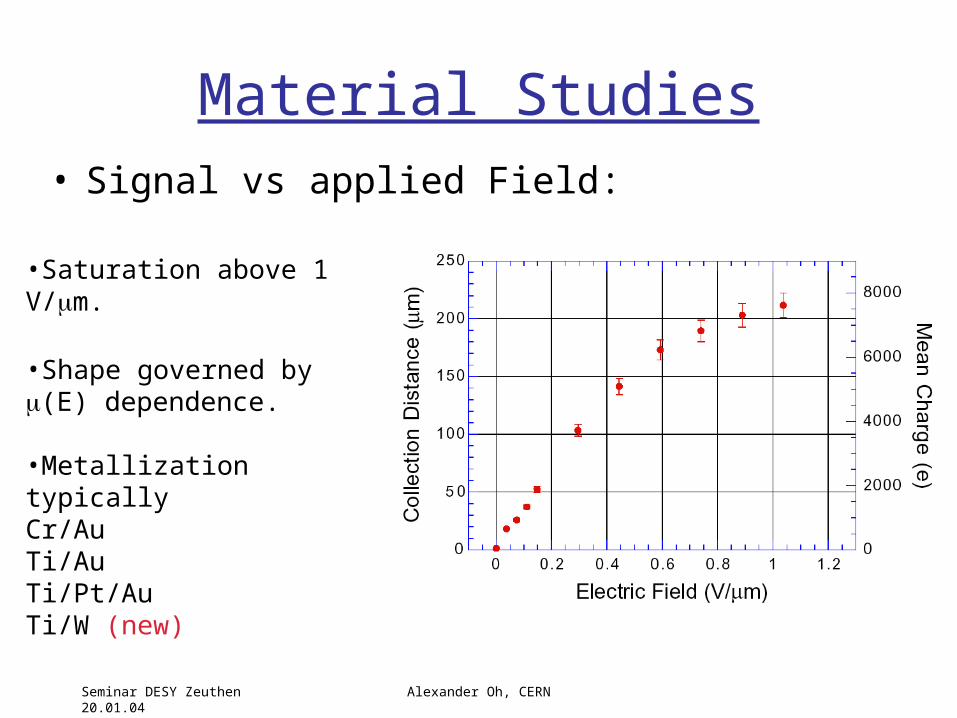
Material Studies• Signal vs applied Field:
•Saturation above 1 V/m.
•Shape governed by (E) dependence.
•Metallization typicallyCr/AuTi/AuTi/Pt/AuTi/W (new)
Seminar DESY Zeuthen 20.01.04 Alexander Oh, CERN
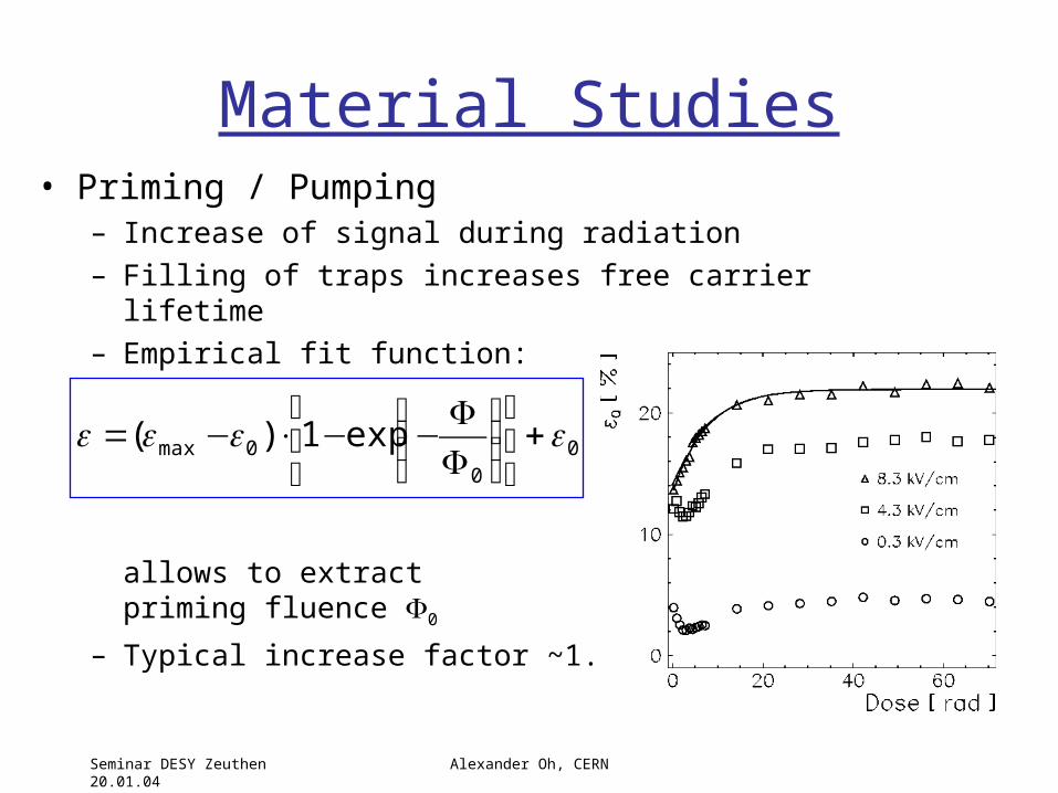
Material Studies• Priming / Pumping
– Increase of signal during radiation– Filling of traps increases free carrier lifetime– Empirical fit function:
–
allows to extract priming fluence 0
– Typical increase factor ~1.5 - 1.8
00
0max exp1)( +⎥⎦
⎤⎢⎣
⎡⎟⎟⎠
⎞⎜⎜⎝
⎛
−−⋅−=
Seminar DESY Zeuthen 20.01.04 Alexander Oh, CERN
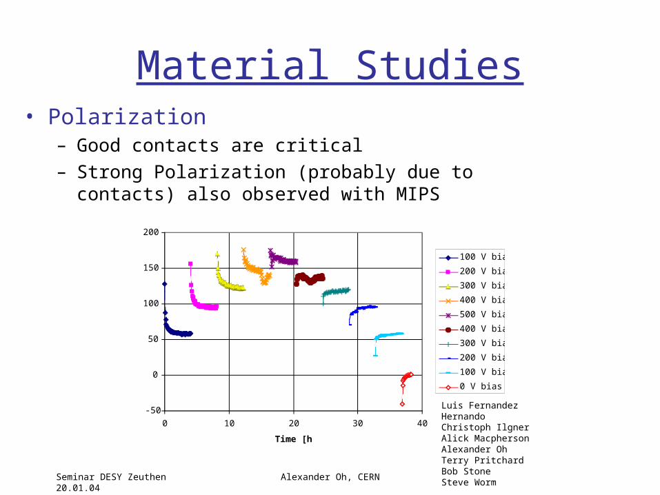
Material Studies• Polarization
– Good contacts are critical– Strong Polarization (probably due to contacts) also observed
with MIPS
-50
0
50
100
150
200
0 10 20 30 40
Time [h]
Collection distance [um]
100 V bias
200 V bias
300 V bias
400 V bias
500 V bias
400 V bias
300 V bias
200 V bias
100 V bias
0 V bias
Luis Fernandez HernandoChristoph IlgnerAlick MacphersonAlexander OhTerry PritchardBob StoneSteve Worm
Seminar DESY Zeuthen 20.01.04 Alexander Oh, CERN
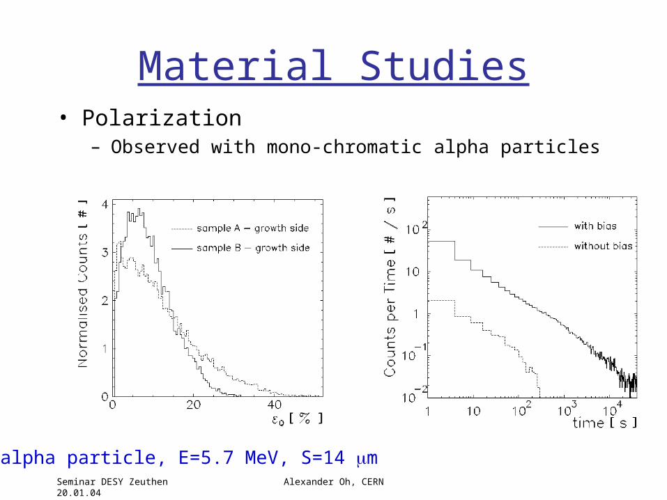
Material Studies
alpha particle, E=5.7 MeV, S=14 m
• Polarization– Observed with mono-chromatic alpha particles
Seminar DESY Zeuthen 20.01.04 Alexander Oh, CERN
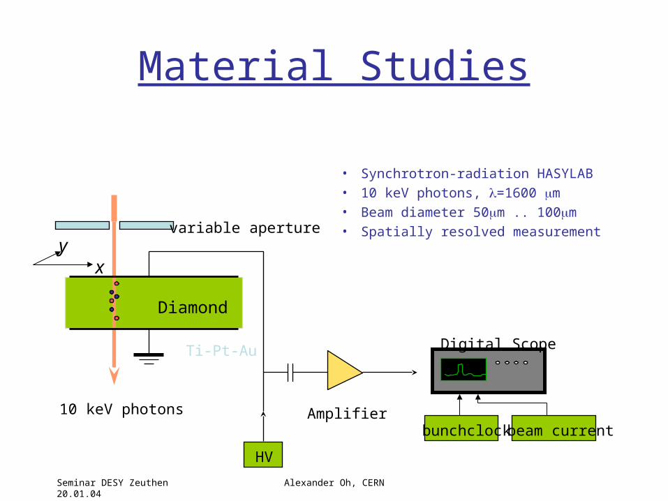
Material Studies
• Synchrotron-radiation HASYLAB
• 10 keV photons, =1600 m
• Beam diameter 50m .. 100m
• Spatially resolved measurement
Diamond
10 keV photons
Ti-Pt-Au
variable aperture
Digital Scope
beam currentbunchclockAmplifier
HV
xy

Seminar DESY Zeuthen 20.01.04 Alexander Oh, CERN
Material Studies• Polycrystalline structure has impacts on
charge collection:
Signal Height [au]F
requ
ency
Seminar DESY Zeuthen 20.01.04 Alexander Oh, CERN
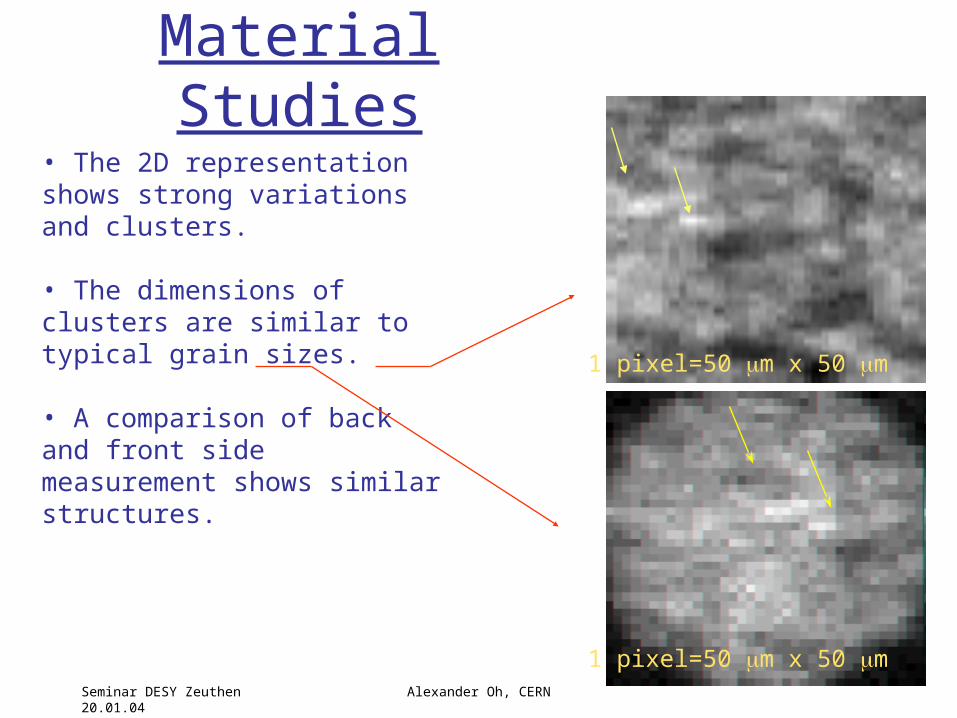
Material Studies• The 2D representation shows strong variations and clusters.
• The dimensions of clusters are similar to typical grain sizes.
• A comparison of back and front side measurement shows similar structures.
1 pixel=50 m x 50 m
1 pixel=50 m x 50 m
Seminar DESY Zeuthen 20.01.04 Alexander Oh, CERN
Material Studies
Leitungsband
Valenzband
Conduction band
Valence band
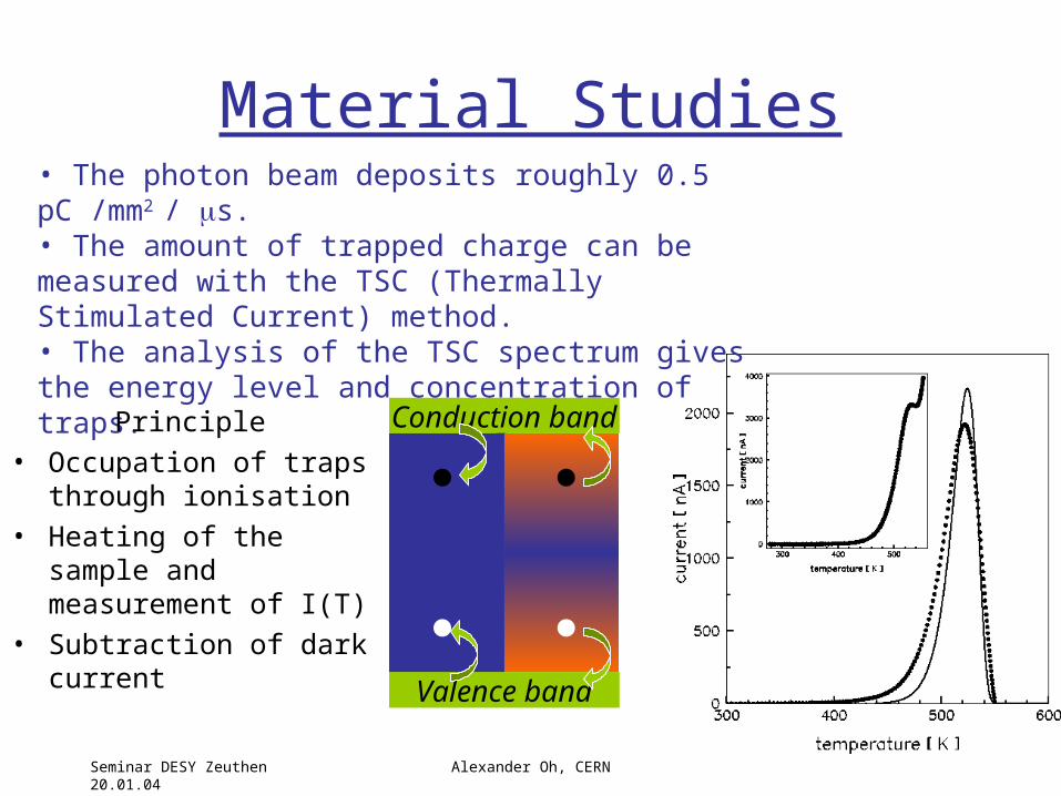
• The photon beam deposits roughly 0.5 pC /mm2 / s. • The amount of trapped charge can be measured with the TSC (Thermally Stimulated Current) method.• The analysis of the TSC spectrum gives the energy level and concentration of traps.
Principle• Occupation of traps
through ionisation • Heating of the sample
and measurement of I(T)
• Subtraction of dark current

Seminar DESY Zeuthen 20.01.04 Alexander Oh, CERN
Material Studies• The photon beam profile defines the volume• After exposure the sample is heated to 300C• The I(T) is recorded• The sample is cooled• The sample is driven to the next scan point
•Irradiation for 30s•Heating time to reach 290C is approx. 30s •Cooling time with LN2 to 0C takes approx. 20s•=> cycle time 1.5 min !
Seminar DESY Zeuthen 20.01.04 Alexander Oh, CERN
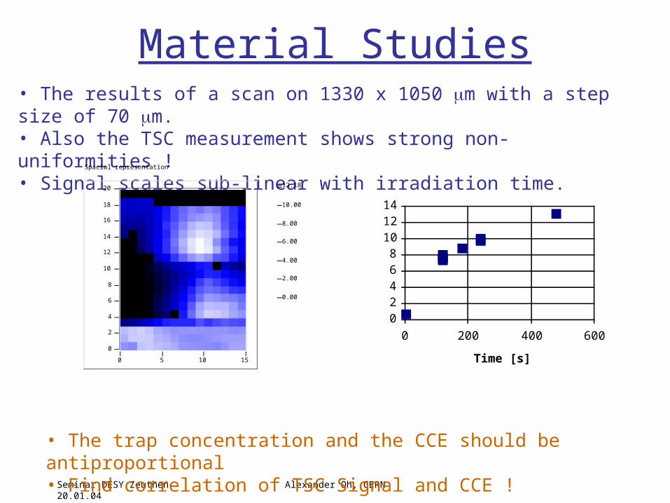
Material Studies• The results of a scan on 1330 x 1050 m with a step size of 70 m.• Also the TSC measurement shows strong non-uniformities !• Signal scales sub-linear with irradiation time.
• The trap concentration and the CCE should be antiproportional• Find correlation of TSC Signal and CCE !
12.18
0.00
2.00
4.00
6.00
8.00
10.00
20
0
2
4
6
8
10
12
14
16
18
150 5 10
Spacial representation
02468
101214
0 200 400 600
Time [s]
Current Integral AU
Seminar DESY Zeuthen 20.01.04 Alexander Oh, CERN
Material Studies
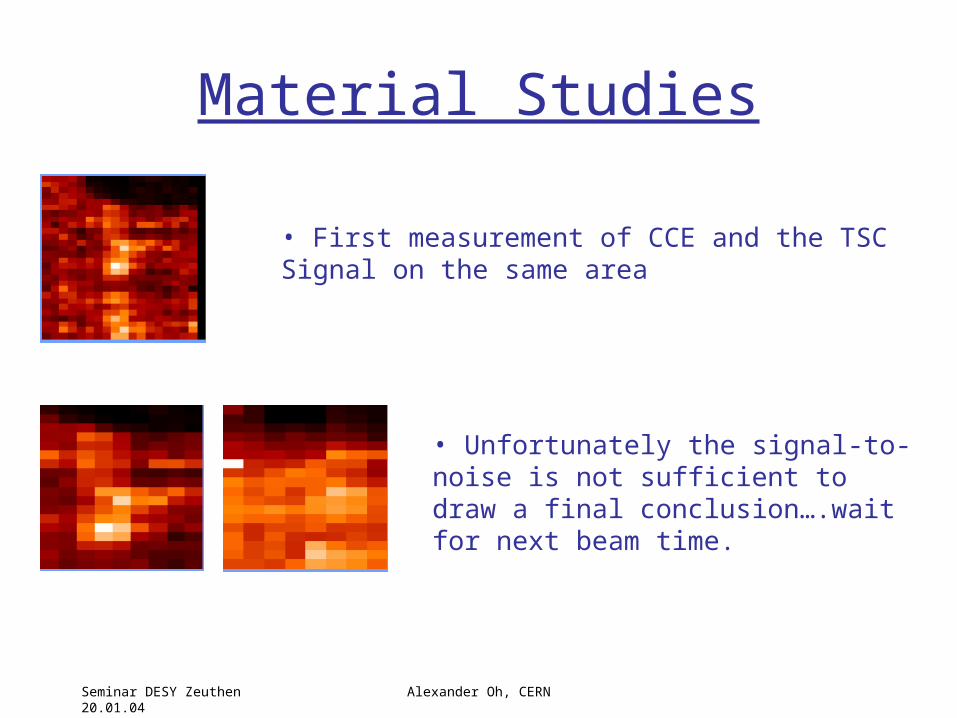
• First measurement of CCE and the TSC Signal on the same area
• Unfortunately the signal-to-noise is not sufficient to draw a final conclusion….wait for next beam time.

Seminar DESY Zeuthen 20.01.04 Alexander Oh, CERN
Material Studies• Growth Side of a recent polycrystalline CVD diamond
Courtesy of Element Six200m
Seminar DESY Zeuthen 20.01.04 Alexander Oh, CERN
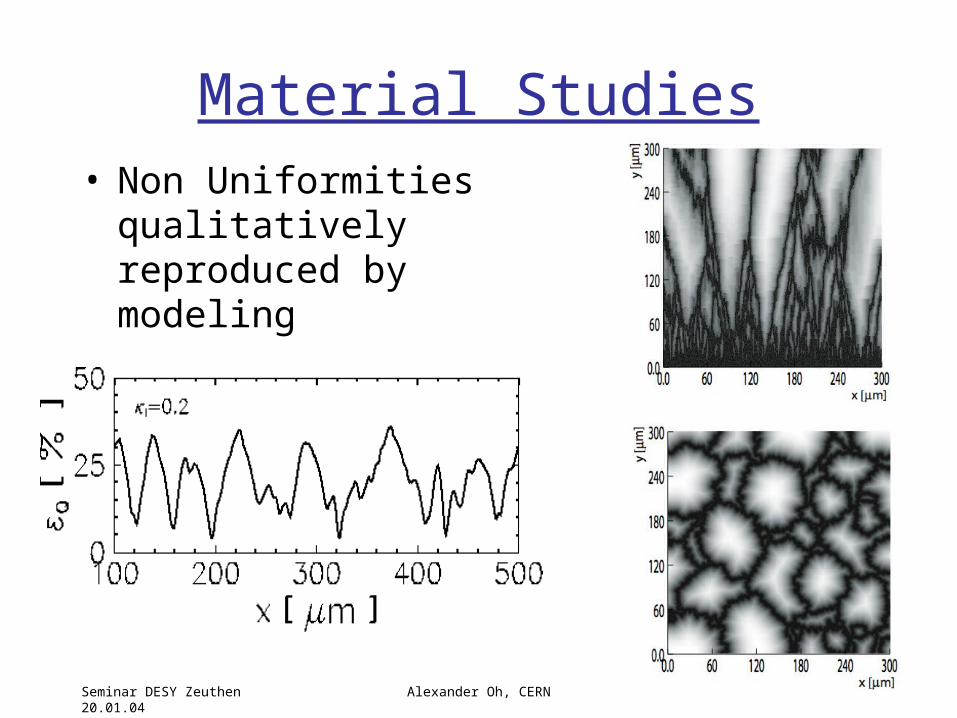
Material Studies• Non Uniformities
qualitatively reproduced by modeling
Seminar DESY Zeuthen 20.01.04 Alexander Oh, CERN
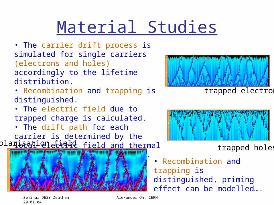
Material Studies• The carrier drift process is simulated for single carriers (electrons and holes) accordingly to the lifetime distribution.• Recombination and trapping is distinguished.• The electric field due to trapped charge is calculated.• The drift path for each carrier is determined by the local electric field and thermal diffusion with 1m resolution.
• Recombination and trapping is distinguished, priming effect can be modelled….
trapped electrons
trapped holespolarisation field
Seminar DESY Zeuthen 20.01.04 Alexander Oh, CERN
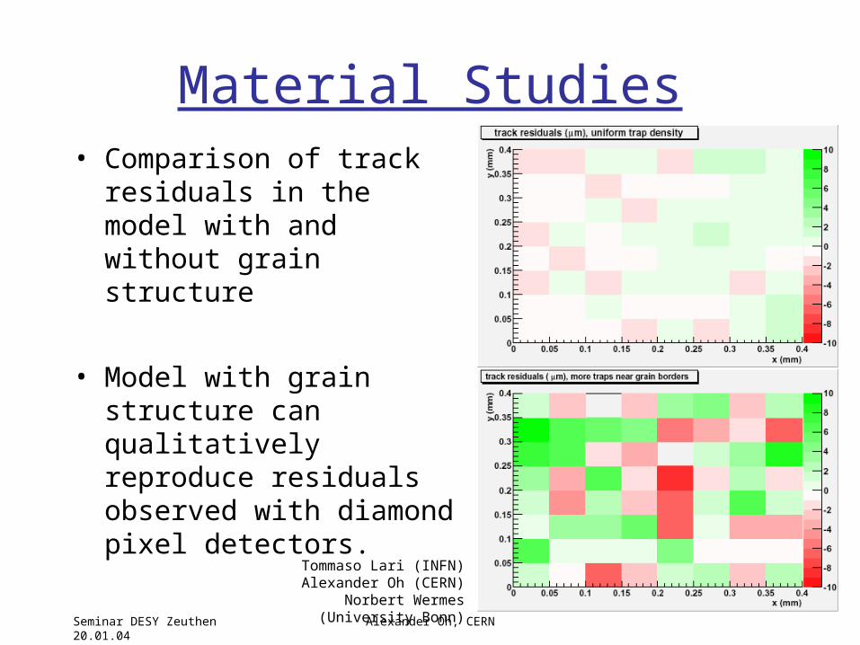
Material Studies• Comparison of track
residuals in the model with and without grain structure
• Model with grain structure can qualitatively reproduce residuals observed with diamond pixel detectors.
Tommaso Lari (INFN)Alexander Oh (CERN)
Norbert Wermes (University Bonn)

Seminar DESY Zeuthen 20.01.04 Alexander Oh, CERN
Material Studies• In 2000 RD42
launched a research program with Element Six to improve the charge collection properties for pCVD diamond.
• Impressive improvements achieved beyond the goal set by RD42.

Seminar DESY Zeuthen 20.01.04 Alexander Oh, CERN
Material Studies• Latest Material measured with 90Sr Source:
Research Program was successful !

Seminar DESY Zeuthen 20.01.04 Alexander Oh, CERN
Material Studies
Thinning Experiment
• successive thinning of sample and remeasuring collection distance
•Gain knowledge on collection properties during growth process
Seminar DESY Zeuthen 20.01.04 Alexander Oh, CERN
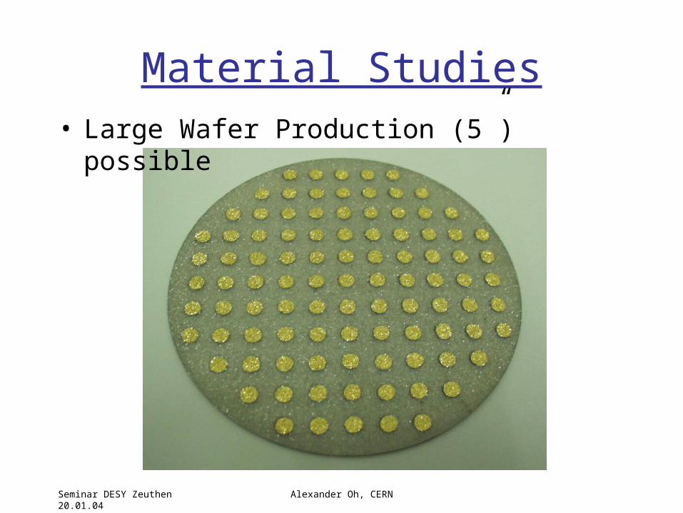
Material Studies• Large Wafer Production (5”) possible

Seminar DESY Zeuthen 20.01.04 Alexander Oh, CERN
Material Studies• Radiation Hardness
– studied with Protons and Pions on pCVD Strip Detectors
– Fluences of 2-3 1015 particles/cm2
– Generally decrease of leakage current with dose observed.
– Resolution of Strip detectors increase with Fluence.
– Pions damage more than protons.– 50% loss of S/N at 2.9 x 10¹⁵ pions/cm2.– No loss seen for EM radiation up to 10MGy.
(Behnke et al., Nucl.Instrum.Meth. A489 (2002) 230-240.)

Seminar DESY Zeuthen 20.01.04 Alexander Oh, CERN
Material Studies• Proton Irradiation
15% loss of S/N 35% improvement in resolution
Seminar DESY Zeuthen 20.01.04 Alexander Oh, CERN
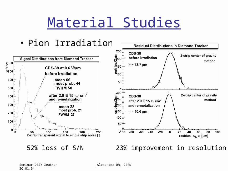
Material Studies• Pion Irradiation
52% loss of S/N 23% improvement in resolution
Seminar DESY Zeuthen 20.01.04 Alexander Oh, CERN
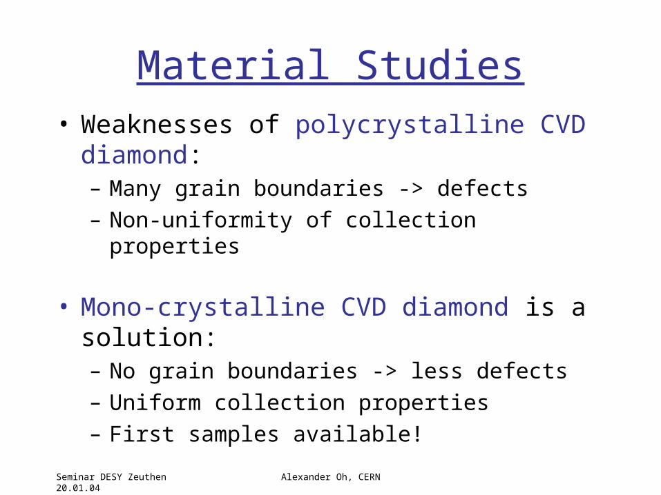
Material Studies• Weaknesses of polycrystalline CVD diamond:
– Many grain boundaries -> defects– Non-uniformity of collection properties
• Mono-crystalline CVD diamond is a solution:– No grain boundaries -> less defects – Uniform collection properties – First samples available!
Seminar DESY Zeuthen 20.01.04 Alexander Oh, CERN
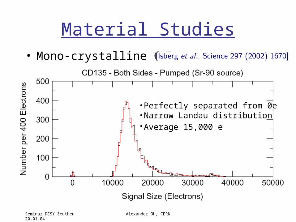
Material Studies• Mono-crystalline CVD
•Perfectly separated from 0e•Narrow Landau distribution•Average 15,000 e
Seminar DESY Zeuthen 20.01.04 Alexander Oh, CERN
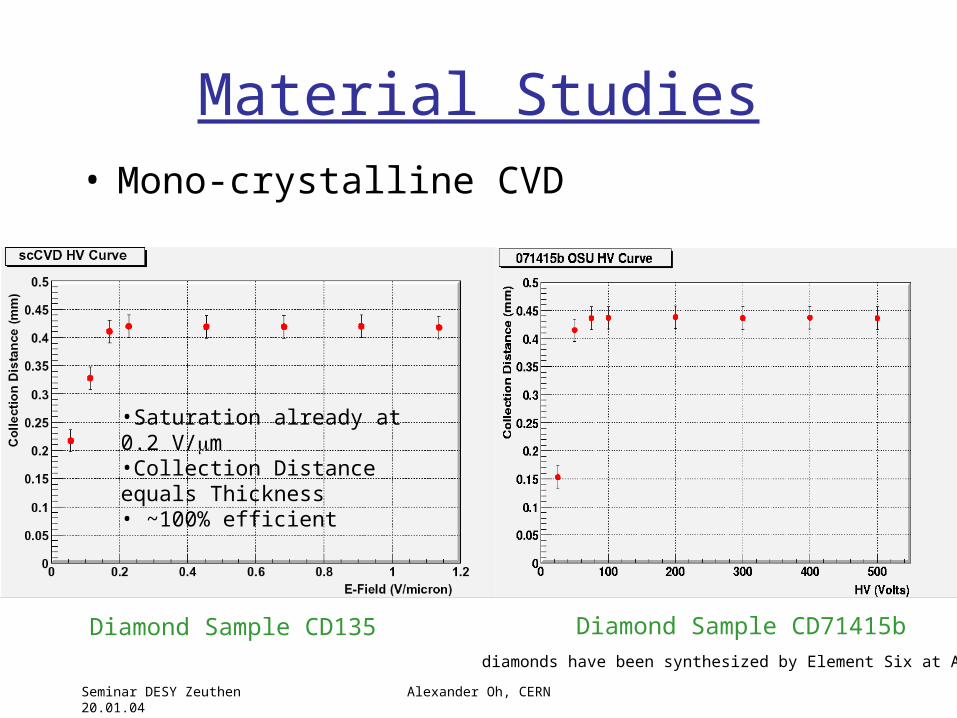
Material Studies• Mono-crystalline CVD
•Saturation already at 0.2 V/m•Collection Distance equals Thickness• ~100% efficient
Diamond Sample CD135 Diamond Sample CD71415b diamonds have been synthesized by Element Six at Ascot

Seminar DESY Zeuthen 20.01.04 Alexander Oh, CERN
Material Studies
• Mono-crystalline CVD– No significant priming
observed– Trap concentration low
Diamond Sample CD135 diamonds have been synthesized by Element Six at Ascot
QuickTime™ and aTIFF (LZW) decompressor
are needed to see this picture.

Seminar DESY Zeuthen 20.01.04 Alexander Oh, CERN
Particle Detector Prototypes

Seminar DESY Zeuthen 20.01.04 Alexander Oh, CERN
Particle Detector Prototypes• Dot detectors
– Characterization
• Strip detectors– Tracking– Slow VA2 and fast LHC electronics
• Pixel detectors– Tracking – CMS and Atlas patterns / electronics
Seminar DESY Zeuthen 20.01.04 Alexander Oh, CERN
Strip Detectors
Seminar DESY Zeuthen 20.01.04 Alexander Oh, CERN
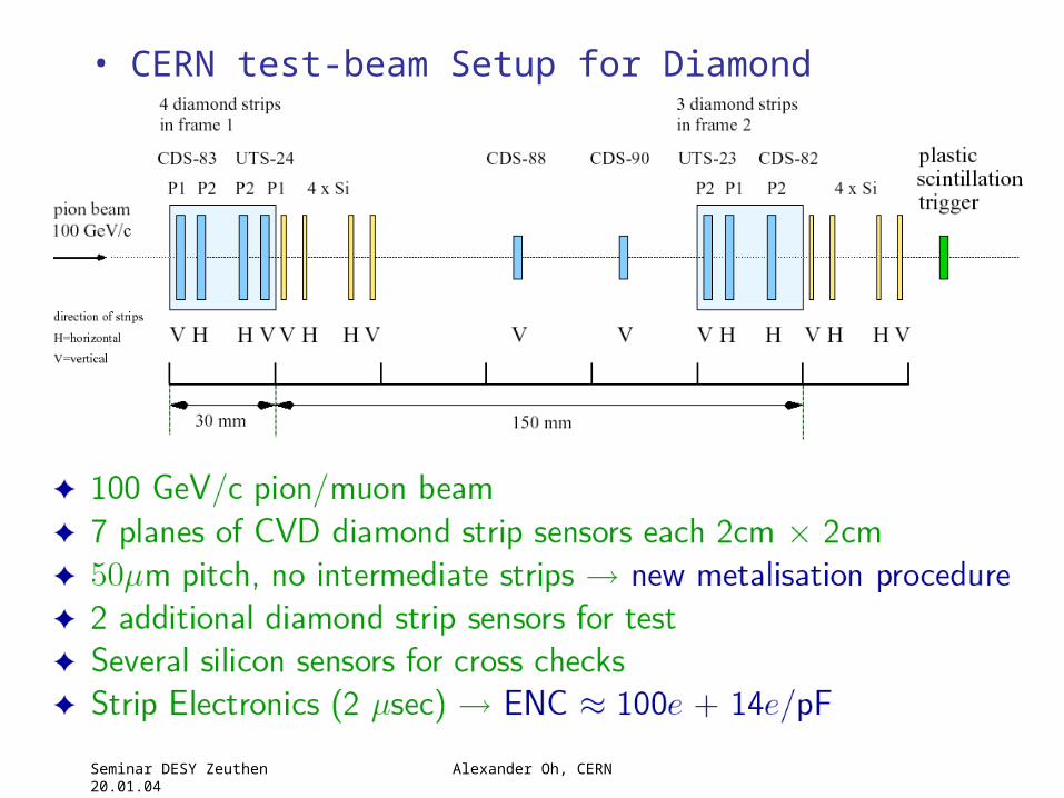
• CERN test-beam Setup for Diamond Telescope

Seminar DESY Zeuthen 20.01.04 Alexander Oh, CERN
• Two planes of the Diamond Telescope

Seminar DESY Zeuthen 20.01.04 Alexander Oh, CERN
Seminar DESY Zeuthen 20.01.04 Alexander Oh, CERN
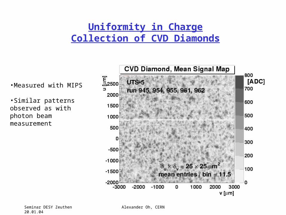
Uniformity in Charge Collection of CVD Diamonds
•Measured with MIPS
•Similar patterns observed as with photon beam measurement

Seminar DESY Zeuthen 20.01.04 Alexander Oh, CERN
• Next Step: • Biased intermediate
strips to benefit from charge sharing.
• Should improve resolution.

Seminar DESY Zeuthen 20.01.04 Alexander Oh, CERN
Pixel Detectors
Seminar DESY Zeuthen 20.01.04 Alexander Oh, CERN
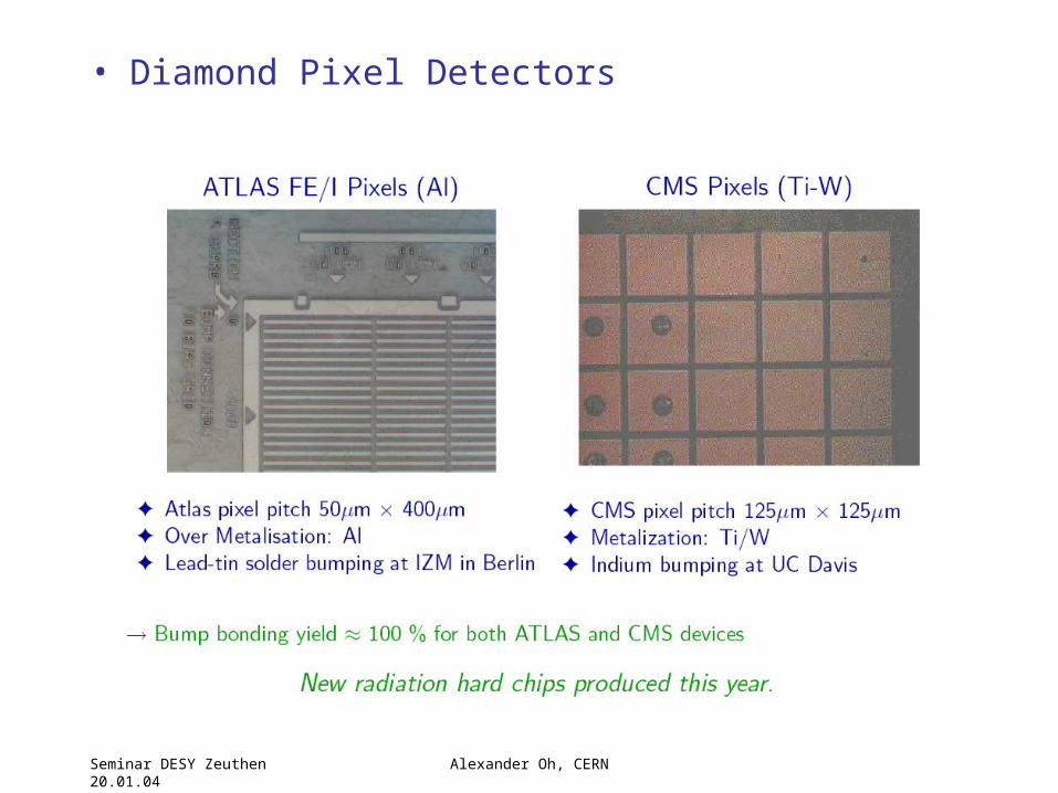
• Diamond Pixel Detectors

Seminar DESY Zeuthen 20.01.04 Alexander Oh, CERN
• Efficiency = 80%• Resolution = digital
• Results from Atlas Diamond Pixel Detectors
=115m=14m

Seminar DESY Zeuthen 20.01.04 Alexander Oh, CERN
• Large track residuals• Non-uniformity of response qualitatively reproduces by modeling
• Results from Atlas Diamond Pixel Detectors
Tommaso Lari (INFN)Alexander Oh (CERN)
Norbert Wermes (University Bonn)

Seminar DESY Zeuthen 20.01.04 Alexander Oh, CERN
• Efficiency = 89% • Resolution = digital
• Results from CMS Diamond Pixel Detectors
Seminar DESY Zeuthen 20.01.04 Alexander Oh, CERN
Applications in HEP

Seminar DESY Zeuthen 20.01.04 Alexander Oh, CERN
Applications in HEP• Vertex detectors with CVD Diamond are not
considered yet as an option for LHC.
• For Beam monitoring CVD Diamond is an option for CMS and ATLAS at the LHC.
• BaBar and Belle test already CVD Diamond in their beam monitoring system.
Seminar DESY Zeuthen 20.01.04 Alexander Oh, CERN
Beam monitoring• For Silicon Vertex systems careful monitoring
is crucial.• Inherently, beam monitors have to be
radiation hard.• Abort Beam when monitors signal dangerous
beam conditions.– False signals must be avoided.– Monitor must be reliable.
• Requirements on the monitoring system depend on the accelerator and vertex system.
Seminar DESY Zeuthen 20.01.04 Alexander Oh, CERN
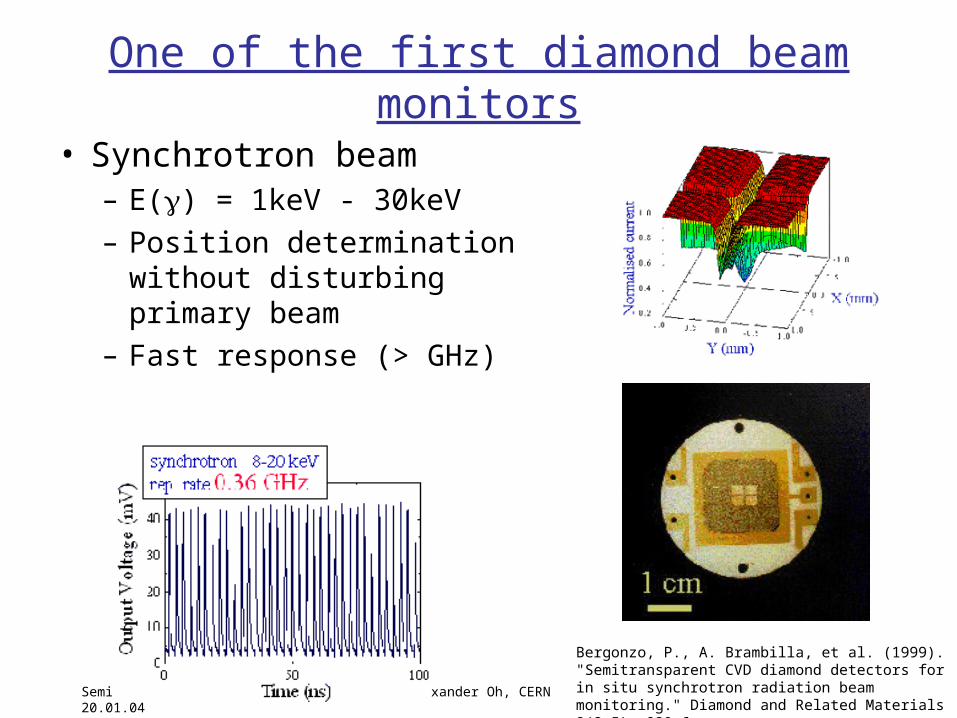
One of the first diamond beam monitors
Bergonzo, P., A. Brambilla, et al. (1999). "Semitransparent CVD diamond detectors for in situ synchrotron radiation beam monitoring." Diamond and Related Materials 8(2-5): 920-6.
• Synchrotron beam– E() = 1keV - 30keV– Position determination
without disturbing primary beam
– Fast response (> GHz)
Seminar DESY Zeuthen 20.01.04 Alexander Oh, CERN
• CMS and Atlas investigate diamond as a sensor for a beam loss and conditions measurements close to the beam pipe.
• Same type of device considered by CMS & Atlas inside their tracker– CMS: ~ z=±1.8m and r=4cm– Atlas: ~ z=±3.5m close to beam pipe
• Act as part of a radiation monitoring system for equipment safety and radiation level/beam monitoring
• A beam conditions monitor can in particular address the following issues:– Allow to protect equipment during instabilities / accidents– Providing feedback to the machine thereby helping them to routinely provide
optimum conditions– Monitor the instantaneous dose during operation
• Advantages of diamond for this application– Radiation hard, low leakage currents at room temperature, fast signal
response• The goal is to detect signs of beam losses and monitor beam conditions
Beam loss and conditions monitor for CMS and Atlas

Seminar DESY Zeuthen 20.01.04 Alexander Oh, CERN
CMS beam monitor• Diamond activity started.• Possible location of Beam Condition Monitors
(BCM) in CMS.
Beam condition monitors
Looking for increase over normal rate
Monitors to be within CMS volume and feed into
machine interlock
Mika Huhtinen, CERN
Expected dose per accident ~1 Gy <=> 1012 protons
Seminar DESY Zeuthen 20.01.04 Alexander Oh, CERN
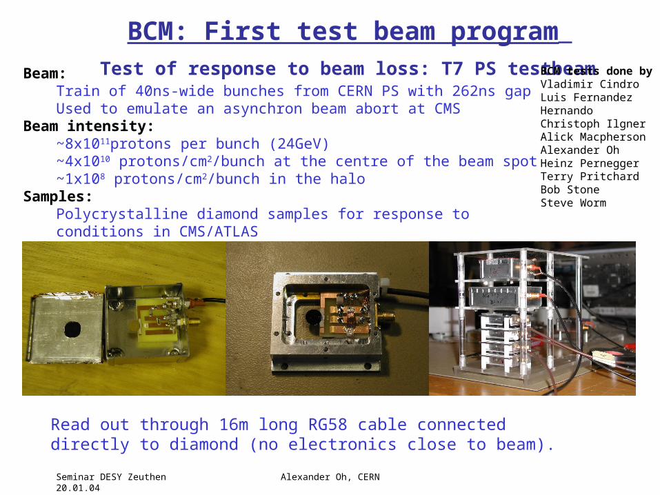
BCM: First test beam program
Test of response to beam loss: T7 PS testbeam
Read out through 16m long RG58 cable connected directly to diamond (no electronics close to beam).
BCM tests done byVladimir CindroLuis Fernandez HernandoChristoph IlgnerAlick MacphersonAlexander OhHeinz PerneggerTerry PritchardBob StoneSteve Worm
Beam: Train of 40ns-wide bunches from CERN PS with 262ns gapUsed to emulate an asynchron beam abort at CMS
Beam intensity: ~8x10¹¹protons per bunch (24GeV)~4x10¹⁰ protons/cm2/bunch at the centre of the beam spot ~1x10⁸ protons/cm2/bunch in the halo
Samples:Polycrystalline diamond samples for response to conditions in CMS/ATLAS

Seminar DESY Zeuthen 20.01.04 Alexander Oh, CERN
BCM Preliminary Results Diamond signal response to high intensity bunch
Almost identical diamond response to PS beam monitor response (pulse length 40ns)
Single pulses from diamond Bias on Diamond = +1 V/um Readout of signal:
16m of cable, no electronics Attenuation on signal cables at scope input Ch 1:20dB (factor 10) Ch 2: 24dB (factor
16)
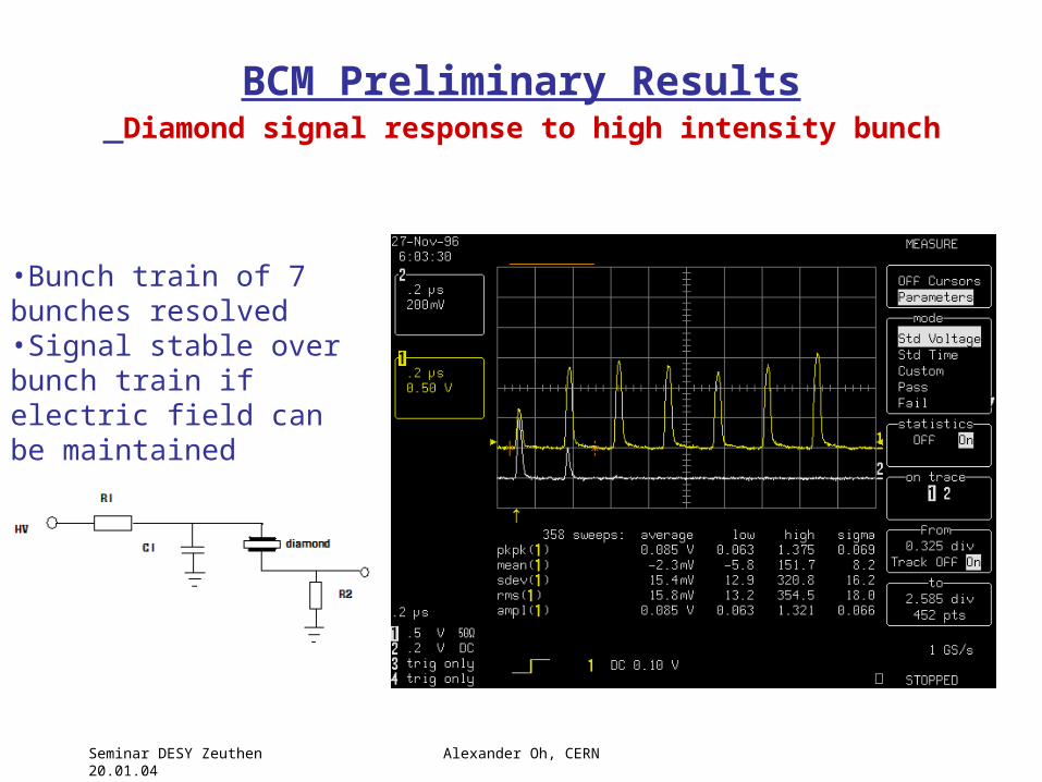
Seminar DESY Zeuthen 20.01.04 Alexander Oh, CERN
BCM Preliminary Results Diamond signal response to high intensity bunch
•Bunch train of 7 bunches resolved•Signal stable over bunch train if electric field can be maintained
Seminar DESY Zeuthen 20.01.04 Alexander Oh, CERN
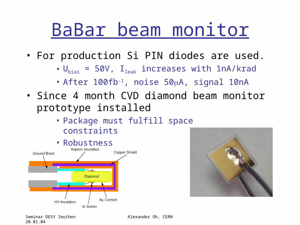
BaBar beam monitor• For production Si PIN diodes are used.
• Ubias = 50V, Ileak increases with 1nA/krad
• After 100fb-1, noise 50A, signal 10nA
• Since 4 month CVD diamond beam monitor prototype installed
• Package must fulfill space constraints
• Robustness
Seminar DESY Zeuthen 20.01.04 Alexander Oh, CERN
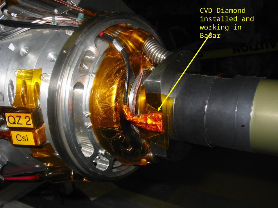
CVD Diamond installed and working in BaBar
Seminar DESY Zeuthen 20.01.04 Alexander Oh, CERN
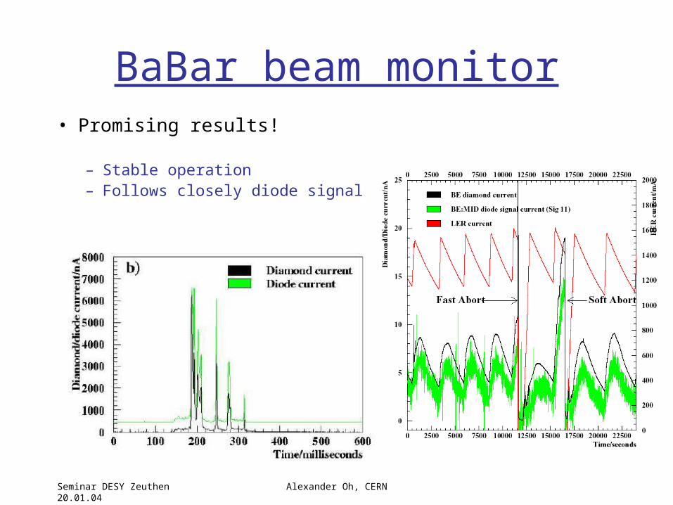
BaBar beam monitor• Promising results!
– Stable operation– Follows closely diode signal
Seminar DESY Zeuthen 20.01.04 Alexander Oh, CERN
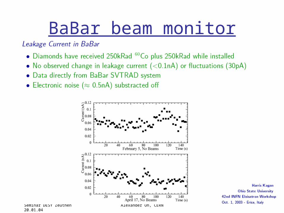
BaBar beam monitor
Seminar DESY Zeuthen 20.01.04 Alexander Oh, CERN
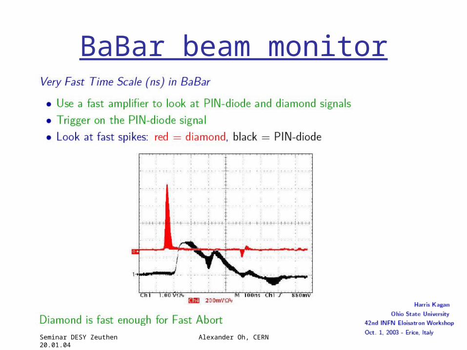
BaBar beam monitor

Seminar DESY Zeuthen 20.01.04 Alexander Oh, CERN
BELLE Diamond Beam Monitor
CVD diamond is installed and working

Seminar DESY Zeuthen 20.01.04 Alexander Oh, CERN
Summary• Charge Collection
– Poly-crystalline CVD diamond:• Most probable signal of ~8000e reached (pCVD)• 99% of charge distribution > 3000e• FWHM / MP ~ 0.95
– Mono-crystalline CVD diamond : • MP signal 13,000e• 99% of charge distribution > 10,000e• FWHM / MP ~ 0.3
Seminar DESY Zeuthen 20.01.04 Alexander Oh, CERN
Summary• Proto-type Detectors
– Dots / Strips / Pixel– Good resolution and S/N 8:1 obtained with rad-
hard electronics– Intermediate Strips are tested this July
• Radiation Hardness– 50% loss of S/N after 2.9 x 10¹⁵ pions/cm2
– No loss seen for EM radiation up to 10MGy.– Will be repeated with newest samples
Seminar DESY Zeuthen 20.01.04 Alexander Oh, CERN
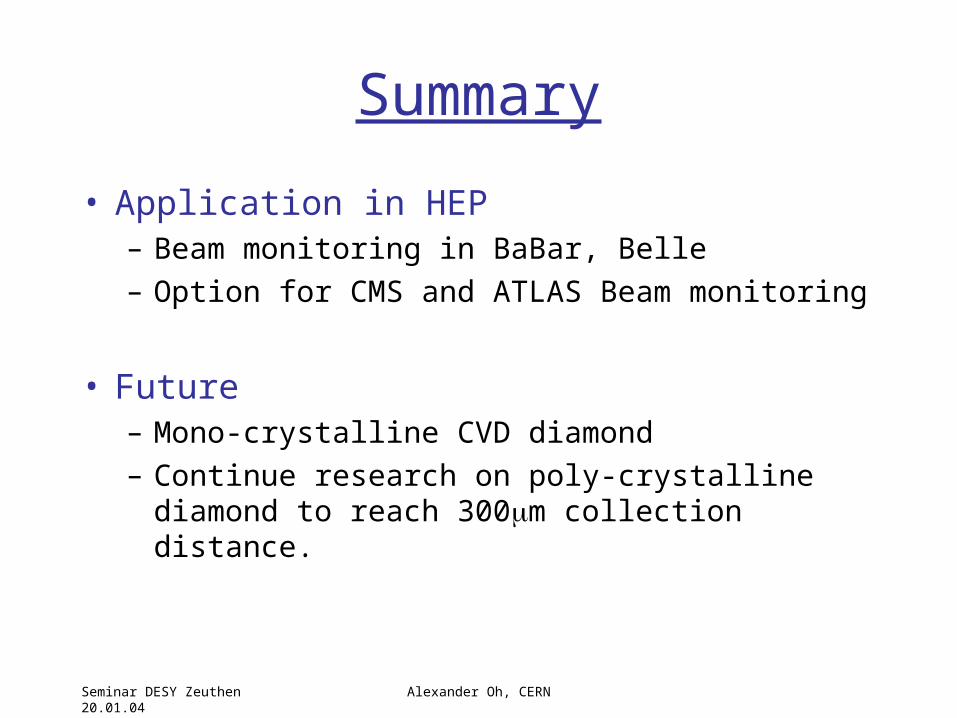
Summary
• Application in HEP– Beam monitoring in BaBar, Belle– Option for CMS and ATLAS Beam monitoring
• Future– Mono-crystalline CVD diamond– Continue research on poly-crystalline diamond to
reach 300m collection distance.


