
SPECIFICATIONS
PXIe-576416-Bit, 1 GS/s, 4-Channel PXI FlexRIO Digitizer
This document lists the specifications for the PXIe-5764. Specifications are subject to changewithout notice. For the most recent device specifications, refer to ni.com/support.
ContentsDefinitions.................................................................................................................................1Conditions................................................................................................................................. 2Digital I/O................................................................................................................................. 2
Digital I/O Single-Ended Channels...................................................................................2Digital I/O High-Speed Serial MGT.................................................................................3
Reconfigurable FPGA...............................................................................................................4Onboard DRAM........................................................................................................................5Analog Input............................................................................................................................. 5
General Characteristics..................................................................................................... 5Typical Specifications....................................................................................................... 5
CLK/REF IN........................................................................................................................... 13General Characteristics................................................................................................... 13
Driver and Application Software............................................................................................ 16Bus Interface........................................................................................................................... 16Maximum Power Requirements..............................................................................................17Physical................................................................................................................................... 17Environment............................................................................................................................17
Operating Environment...................................................................................................17Storage Environment.......................................................................................................17
Shock and Vibration................................................................................................................18TCLK Specifications...............................................................................................................18
Intermodule Synchronization Using NI-TClk for Identical Modules.............................18
DefinitionsWarranted specifications describe the performance of a model under stated operatingconditions and are covered by the model warranty.

Characteristics describe values that are relevant to the use of the model under stated operatingconditions but are not covered by the model warranty.• Typical specifications describe the performance met by a majority of models.• Nominal specifications describe an attribute that is based on design, conformance testing,
or supplemental testing.• Measured specifications describe the measured performance of a representative model.
Specifications are Typical unless otherwise noted.
ConditionsSpecifications are valid under the following conditions unless otherwise noted.• Ambient temperature of 23 °C ± 5 °C• Installed in chassis with slot cooling capacity ≥58 W
Digital I/OConnector Molex™ Nano-Pitch I/O™
5.0 V Power ±5%, 50 mA maximum, nominal
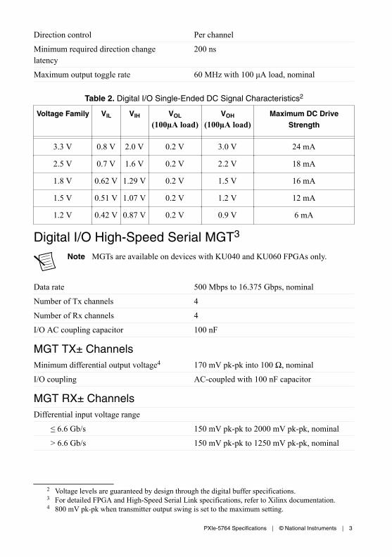
Table 1. Digital I/O Signal Characteristics
Signal Type Direction
MGT Tx± <3..0>1 Xilinx UltraScale GTH Output
MGT Rx± <3..0>1 Xilinx UltraScale GTH Input
DIO <7..0> Single-ended Bidirectional
5.0 V DC Output
GND Ground —
Digital I/O Single-Ended ChannelsNumber of channels 8
Signal type Single-ended
Voltage families 3.3 V, 2.5 V, 1.8 V, 1.5 V, 1.2 V
Input impedance 100 kΩ, nominal
Output impedance 50 Ω, nominal
1 Multi-gigabit transceiver (MGT) signals are available on devices with KU040 and KU060 FPGAsonly.
2 | ni.com | PXIe-5764 Specifications
Direction control Per channel
Minimum required direction changelatency
200 ns
Maximum output toggle rate 60 MHz with 100 μA load, nominal
Table 2. Digital I/O Single-Ended DC Signal Characteristics2
Voltage Family VIL VIH VOL
(100µA load)VOH
(100µA load)Maximum DC Drive
Strength
3.3 V 0.8 V 2.0 V 0.2 V 3.0 V 24 mA
2.5 V 0.7 V 1.6 V 0.2 V 2.2 V 18 mA
1.8 V 0.62 V 1.29 V 0.2 V 1.5 V 16 mA
1.5 V 0.51 V 1.07 V 0.2 V 1.2 V 12 mA
1.2 V 0.42 V 0.87 V 0.2 V 0.9 V 6 mA
Digital I/O High-Speed Serial MGT3
Note MGTs are available on devices with KU040 and KU060 FPGAs only.
Data rate 500 Mbps to 16.375 Gbps, nominal
Number of Tx channels 4
Number of Rx channels 4
I/O AC coupling capacitor 100 nF
MGT TX± ChannelsMinimum differential output voltage4 170 mV pk-pk into 100 Ω, nominal
I/O coupling AC-coupled with 100 nF capacitor
MGT RX± ChannelsDifferential input voltage range
≤ 6.6 Gb/s 150 mV pk-pk to 2000 mV pk-pk, nominal
> 6.6 Gb/s 150 mV pk-pk to 1250 mV pk-pk, nominal
2 Voltage levels are guaranteed by design through the digital buffer specifications.3 For detailed FPGA and High-Speed Serial Link specifications, refer to Xilinx documentation.4 800 mV pk-pk when transmitter output swing is set to the maximum setting.
PXIe-5764 Specifications | © National Instruments | 3

Differential input resistance 100 Ω, nominal
I/O coupling DC-coupled, requires external capacitor
Reconfigurable FPGAPXIe-5764 modules are available with multiple FPGA options. The following table lists theFPGA specifications for the PXIe-5764 FPGA options.
Table 3. Reconfigurable FPGA Options
KU035 KU040 KU060
LUTs 203,128 242,200 331,680
DSP48 slices(25 × 18 multiplier)
1,700 1,920 2,760
Embedded Block RAM 19.0 Mb 21.1 Mb 38.0 Mb
Default timebase 80 MHz
Timebase reference sources PXI Express 100 MHz (PXIe_CLK100)
Data transfers DMA, interrupts,programmed I/O
DMA, interrupts, programmed I/O,multi-gigabit transceivers
Number of DMA channels 60
Note The Reconfigurable FPGA Options table depicts the total number of FPGAresources available on the part. The number of resources available to the user isslightly lower, as some FPGA resources are consumed by board-interfacing IP forPCI Express, device configuration, and various board I/O. For more information,contact NI support.
Note For FPGA designs using the majority of KU040 or KU060 FPGA resourceswhile running at clock rates over 150 MHz, the module may require more powerthan is available. If the module attempts to draw more than allowed per itsspecification, the module protects itself and reverts to a default FPGA personality.Refer to the getting started guide for your module or contact NI support for moreinformation.
4 | ni.com | PXIe-5764 Specifications
Onboard DRAMNote DRAM is available on devices with KU040 and KU060 FPGAs only.
Memory size 4 GB (2 banks of 2 GB)
DRAM clock rate 1064 MHz
Physical bus width 32 bit
LabVIEW FPGA DRAM clock rate 267 MHz
LabVIEW FPGA DRAM bus width 256 bit per bank
Maximum theoretical data rate 17 GB/s (8.5 GB/s per bank)
Analog InputNotice The maximum input signal levels are valid only when the module ispowered on. To avoid permanent damage to the PXIe-5764, do not apply a signal tothe device when the module is powered down.
General CharacteristicsNumber of channels 4, single-ended, simultaneously sampled
Connector type SMA
Input impedance 50 Ω
Input coupling AC or DC5
Sample rate
Internal Sample Clock 1 GHz
External Sample Clock 1 GHz
Analog-to-digital converter (ADC) ADS54J60, 16-bit resolution
Typical SpecificationsFull-scale input range (normal operating conditions)
AC-coupled 2.05 Vpp (10.22 dBm) at 10 MHz
DC-coupled 2.00 Vpp (10 dBm)
5 Only one analog input path type is populated.
PXIe-5764 Specifications | © National Instruments | 5
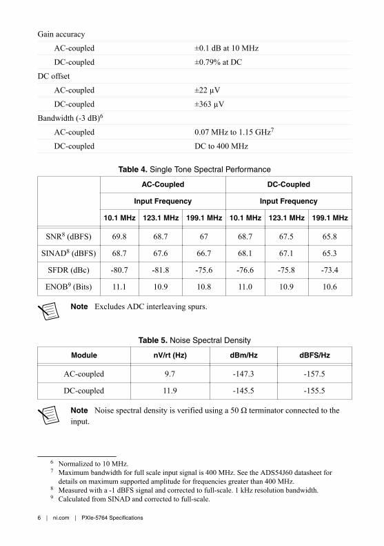
Gain accuracy
AC-coupled ±0.1 dB at 10 MHz
DC-coupled ±0.79% at DC
DC offset
AC-coupled ±22 µV
DC-coupled ±363 µV
Bandwidth (-3 dB)6
AC-coupled 0.07 MHz to 1.15 GHz7
DC-coupled DC to 400 MHz
Table 4. Single Tone Spectral Performance
AC-Coupled DC-Coupled
Input Frequency Input Frequency
10.1 MHz 123.1 MHz 199.1 MHz 10.1 MHz 123.1 MHz 199.1 MHz
SNR8 (dBFS) 69.8 68.7 67 68.7 67.5 65.8
SINAD8 (dBFS) 68.7 67.6 66.7 68.1 67.1 65.3
SFDR (dBc) -80.7 -81.8 -75.6 -76.6 -75.8 -73.4
ENOB9 (Bits) 11.1 10.9 10.8 11.0 10.9 10.6
Note Excludes ADC interleaving spurs.
Table 5. Noise Spectral Density
Module nV/rt (Hz) dBm/Hz dBFS/Hz
AC-coupled 9.7 -147.3 -157.5
DC-coupled 11.9 -145.5 -155.5
Note Noise spectral density is verified using a 50 Ω terminator connected to theinput.
6 Normalized to 10 MHz.7 Maximum bandwidth for full scale input signal is 400 MHz. See the ADS54J60 datasheet for
details on maximum supported amplitude for frequencies greater than 400 MHz.8 Measured with a -1 dBFS signal and corrected to full-scale. 1 kHz resolution bandwidth.9 Calculated from SINAD and corrected to full-scale.
6 | ni.com | PXIe-5764 Specifications

Figure 1. AC-Coupled Single Tone Spectrum (10.1 MHz, -1 dBFS, 1 kHz RBW),Measured
Figure 2. AC-Coupled Single Tone Spectrum (123.1 MHz, -1 dBFS, 1 kHz RBW),Measured
PXIe-5764 Specifications | © National Instruments | 7

Figure 3. AC-Coupled Single Tone Spectrum (199.1 MHz, -1 dBFS, 1 kHz RBW),Measured
Figure 4. DC-Coupled Single Tone Spectrum (10.1 MHz, -1 dBFS, 1 kHz RBW),Measured
8 | ni.com | PXIe-5764 Specifications
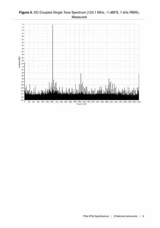
Figure 5. DC-Coupled Single Tone Spectrum (123.1 MHz, -1 dBFS, 1 kHz RBW),Measured
PXIe-5764 Specifications | © National Instruments | 9

Figure 6. DC-Coupled Single Tone Spectrum (199.1 MHz, -1 dBFS, 1 kHz RBW),Measured
Channel-to-channel crosstalk AC-coupled, measured
1 MHz -87 dB
100 MHz -90 dB
250 MHz -85 dB
400 MHz -84 dB
Channel-to-channel crosstalk DC-coupled, measured
1 MHz -88 dB
100 MHz -84 dB
250 MHz -75 dB
400 MHz -75 dB
10 | ni.com | PXIe-5764 Specifications
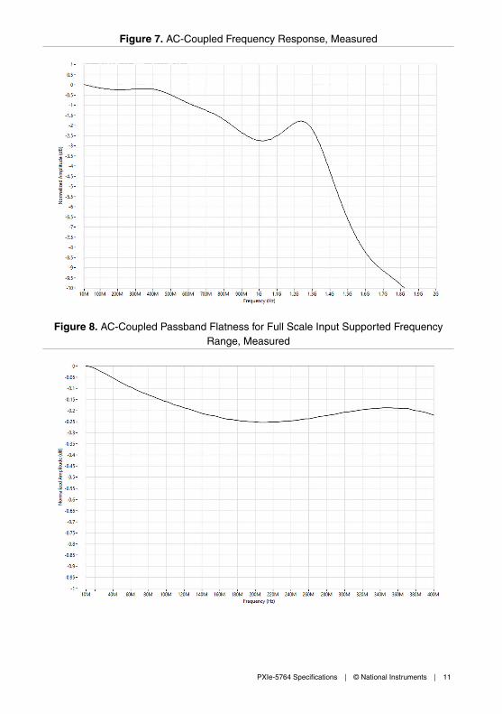
Figure 7. AC-Coupled Frequency Response, Measured
Figure 8. AC-Coupled Passband Flatness for Full Scale Input Supported FrequencyRange, Measured
PXIe-5764 Specifications | © National Instruments | 11

Figure 9. DC-Coupled Frequency Response, Measured
Figure 10. DC-Coupled Frequency Response Zoomed In, Measured
12 | ni.com | PXIe-5764 Specifications
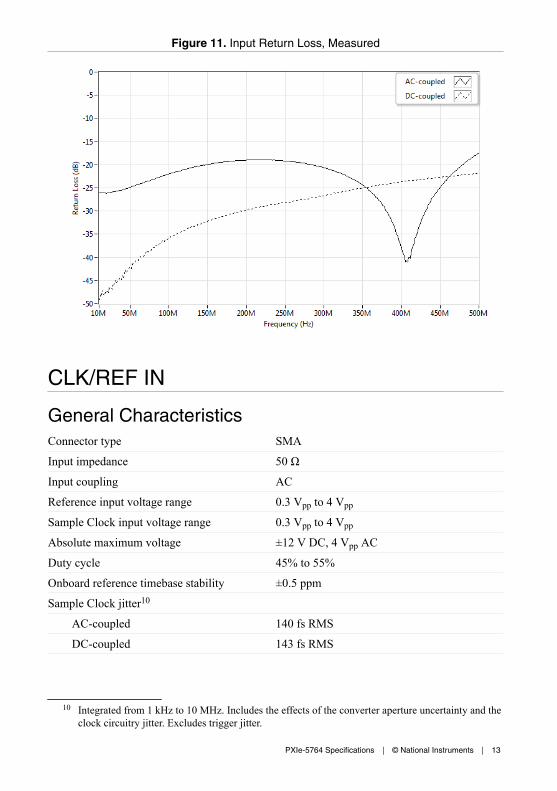
Figure 11. Input Return Loss, Measured
CLK/REF IN
General CharacteristicsConnector type SMA
Input impedance 50 Ω
Input coupling AC
Reference input voltage range 0.3 Vpp to 4 Vpp
Sample Clock input voltage range 0.3 Vpp to 4 Vpp
Absolute maximum voltage ±12 V DC, 4 Vpp AC
Duty cycle 45% to 55%
Onboard reference timebase stability ±0.5 ppm
Sample Clock jitter10
AC-coupled 140 fs RMS
DC-coupled 143 fs RMS
10 Integrated from 1 kHz to 10 MHz. Includes the effects of the converter aperture uncertainty and theclock circuitry jitter. Excludes trigger jitter.
PXIe-5764 Specifications | © National Instruments | 13

Table 6. Clock Configuration Options
Clock ConfigurationExternal
Clock Type
ExternalClock
FrequencyDescription
Internal ReferenceClock11
— — The internal Sample Clock locks toan onboard voltage-controlledtemperature compensated crystaloscillator (VCTCXO).
Internal PXI_CLK10 — 10 MHz The internal Sample Clock locks tothe PXI 10 MHz Reference Clock,which is provided through thebackplane.
External ReferenceClock (CLK/REF IN)
ReferenceClock
10 MHz12 The internal Sample Clock locks toan external Reference Clock,which is provided through theCLK/REF IN front panelconnector.
External SampleClock (CLK/REF IN)
Sample Clock 1 GHz An external Sample Clock can beprovided through the CLK/REF INfront panel connector.
11 Default clock configuration.12 The PLL Reference Clock must be accurate to ±25 ppm.
14 | ni.com | PXIe-5764 Specifications
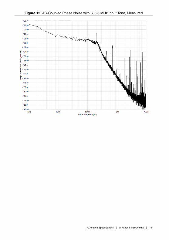
Figure 12. AC-Coupled Phase Noise with 385.6 MHz Input Tone, Measured
PXIe-5764 Specifications | © National Instruments | 15
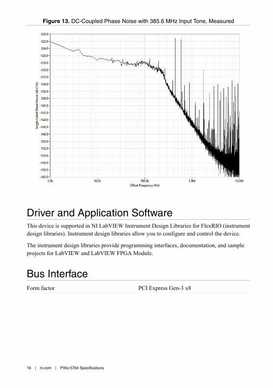
Figure 13. DC-Coupled Phase Noise with 385.6 MHz Input Tone, Measured
Driver and Application SoftwareThis device is supported in NI LabVIEW Instrument Design Libraries for FlexRIO (instrumentdesign libraries). Instrument design libraries allow you to configure and control the device.
The instrument design libraries provide programming interfaces, documentation, and sampleprojects for LabVIEW and LabVIEW FPGA Module.
Bus InterfaceForm factor PCI Express Gen-3 x8
16 | ni.com | PXIe-5764 Specifications
Maximum Power RequirementsNote Power requirements are dependent on the contents of the LabVIEW FPGAVI used in your application.
+3.3 V 3 A
+12 V 4 A
Maximum total power 58 W
PhysicalDimensions (not including connectors) 18.8 cm × 12.9 cm (7.4 in. × 5.1 in.)
Weight 190 g (6.7 oz)
Note Clean the hardware with a soft, nonmetallic brush. Make sure that thehardware is completely dry and free of contaminants before returning it to service.
EnvironmentMaximum altitude 2,000 m (800 mbar) (at 25 °C ambient
temperature)
Pollution Degree 2
Indoor use only.
Operating EnvironmentAmbient temperature range 0 °C to 55 °C13
Relative humidity range 10% to 90%, noncondensing
Storage EnvironmentAmbient temperature range -40 °C to 71 °C (Tested in accordance
with IEC 60068-2-1 and IEC 60068-2-2. MeetsMIL-PRF-28800F Class 4 limits.)
Relative humidity range 5% to 95%, noncondensing (Tested inaccordance with IEC 60068-2-56.)
13 The PXIe-5764 requires a chassis with slot cooling capacity ≥58 W. Not all chassis with slotcooling capacity ≥58 W can achieve this ambient temperature range. Refer to the PXI ChassisManual for specifications to determine the ambient temperature ranges your chassis can achieve.
PXIe-5764 Specifications | © National Instruments | 17

Shock and VibrationOperating shock 30 g peak, half-sine, 11 ms pulse (Tested in
accordance with IEC 60068-2-27. MeetsMIL-PRF-28800F Class 2 limits.)
Random vibration
Operating 5 Hz to 500 Hz, 0.3 grms (Tested in accordancewith IEC 60068-2-64.)
Nonoperating 5 Hz to 500 Hz, 2.4 grms (Tested in accordancewith IEC 60068-2-64. Test profile exceeds therequirements of MIL-PRF-28800F, Class 3.)
TCLK Specifications
You can use the NI TClk synchronization method and the NI-TClk driver to align the SampleClocks on any number of supported devices, in one or more chassis. For more informationabout TClk synchronization, refer to the NI-TClk Synchronization Help within the FlexRIOHelp. For other configurations, including multichassis systems, contact NI Technical Supportat ni.com/support.
Intermodule Synchronization Using NI-TClk forIdentical ModulesSynchronization specifications are valid under the following conditions:• All modules are installed in one PXI Express chassis.• The NI-TClk driver is used to align the Sample Clocks of each module.• All parameters are set to identical values for each module.• Modules are synchronized without using an external Sample Clock.
Note Although you can use NI-TClk to synchronize non-identical modules, thesespecifications apply only to synchronizing identical modules.
Skew14
AC-coupled 120 ps, measured
DC-coupled 190 ps, measured
14 Caused by clock and analog delay differences. No manual adjustment performed. Tested with aPXIe-1085 chassis with a 24 GB backplane with a maximum slot to slot skew of 100 ps. Measuredat 23 °C.
18 | ni.com | PXIe-5764 Specifications
Skew after manual adjustment ≤10 ps, measured
Sample Clock delay/adjustment 1.5 ps
PXIe-5764 Specifications | © National Instruments | 19

Information is subject to change without notice. Refer to the NI Trademarks and Logo Guidelines at ni.com/trademarks forinformation on NI trademarks. Other product and company names mentioned herein are trademarks or trade names of theirrespective companies. For patents covering NI products/technology, refer to the appropriate location: Help»Patents in yoursoftware, the patents.txt file on your media, or the National Instruments Patent Notice at ni.com/patents. You can findinformation about end-user license agreements (EULAs) and third-party legal notices in the readme file for your NI product. Referto the Export Compliance Information at ni.com/legal/export-compliance for the NI global trade compliance policy and howto obtain relevant HTS codes, ECCNs, and other import/export data. NI MAKES NO EXPRESS OR IMPLIED WARRANTIES ASTO THE ACCURACY OF THE INFORMATION CONTAINED HEREIN AND SHALL NOT BE LIABLE FOR ANY ERRORS. U.S.Government Customers: The data contained in this manual was developed at private expense and is subject to the applicablelimited rights and restricted data rights as set forth in FAR 52.227-14, DFAR 252.227-7014, and DFAR 252.227-7015.
© 2018—2020 National Instruments. All rights reserved.
376461C-01 January 27, 2020


