Pulsed Power EngineeringAdvanced Topologies
June 13-17, 2011
Craig Burkhart & Mark KempPower Conversion Department
SLAC National Accelerator Laboratory
June 13 - 17, 2011 2
Advanced Modulator Topologies• Marx
– Basic Marx– Solid state Marx– Inversion generator– Stacked Blumlein– PFN Marx
• Adder topologies– Inductive– Transmission line
• Resonant converter-modulator• Magnetic pulse compression
– Magnetic modulator– Branched magnetics
• Opening switch PFL
USPAS Pulsed Power Engineering Burkhart & Kemp

June 13 - 17, 2011 3
Basic Marx Generator• Concept first proposed by E. Marx in 1925
– Charge capacitors in parallel• Maximum voltage: V• Total capacitance: NC
– Discharge them in series• Maximum voltage: NV• Total capacitance: C/N
• Applicable over wide range of parameters– Sub-μs < pulse length < multi-ms– ~0.1 MV < output voltage < over 10 MV
• Simplifies voltage insulation and reduces switch voltage by factor of N (up to ~100)
– Relatively low voltage on long time scales (charging) – High voltage only present while being delivered to load
USPAS Pulsed Power Engineering Burkhart & Kemp

June 13 - 17, 2011 4
Basic Marx Generator• Necessitates isolation elements between stages (R or L typically) that
can hold off V• Waveform subject to distortion
– Reduced output voltage– Slow risetime– Impaired stage triggering
Due to parasitic circuit elements– Capacitance
• Stage-to-stage• Stage-to-ground
– Inductance• Switch• Capacitor• Leads/layout
USPAS Pulsed Power Engineering Burkhart & Kemp

June 13 - 17, 2011 USPAS Pulsed Power Engineering: TTU PPSC 5
Basic Marx Generator

June 13 - 17, 2011 USPAS Pulsed Power Engineering: TTU PPSC 6
Basic Marx Generator (cont.)

June 13 - 17, 2011 USPAS Pulsed Power Engineering: TTU PPSC 7
Impact of Parasitic Capacitance on Marx Voltage

June 13 - 17, 2011 USPAS Pulsed Power Engineering: TTU PPSC 8
Impact of Parasitic Capacitance on Marx Voltage

June 13 - 17, 2011 USPAS Pulsed Power Engineering: TTU PPSC 9
Impact of Parasitic Capacitance on Marx Voltage
2% parasitic capacitance reduces output voltage by 30%

June 13 - 17, 2011 USPAS Pulsed Power Engineering: TTU PPSC 10
Impact of Parasitic Capacitance on Marx Voltage

June 13 - 17, 2011 USPAS Pulsed Power Engineering: TTU PPSC 11
Impact of Parasitic Capacitance on Marx Voltage

June 13 - 17, 2011 USPAS Pulsed Power Engineering: TTU PPSC 12
Marx Charging Options

June 13 - 17, 2011 USPAS Pulsed Power Engineering: TTU PPSC 13
Marx Charging Options (cont.)
June 13 - 17, 2011 14
Solid State Marx• Use as a voltage multiplier to array solid state switches to klystron
voltage requirements– Output ~0.1 MV– Cells ~few kV– Square output waveform
• Hard switch (close/open) topology• Controlled switching of each cell
– High average power– High PRF (> Hz)– Long life
• Solid state charging/isolation elements – Low loss– Minimize recharge time
USPAS Pulsed Power Engineering Burkhart & Kemp

June 13 - 17, 2011 15
Simplified Schematic of ILC-Marx P1-Prototype
• Marx Topology: Charge Cells in Parallel, Discharge in Series
• 11kV per Cell• 16 Cells
– 11 prompt cells → 120 kV– 5 delay cells, compensates capacitor
droop• Cell High Voltage Switches
– Array of 4.5kV, 60A IGBTs 3 parallel X 5 series
– Fire switches erect Marx– Charge switches provide current return
path for main charging supply (-11 kV) and auxiliary power (-300 V)
• Diode Strings Provide Isolation Between Cells When Marx Erects
– 18 series 1200 V, 60A, Ultrafast Soft Recovery Type
– Parallel Resistors and MOVs to balance & protect against over-voltage
• Inductors Limit Fault dI/dt
USPAS Pulsed Power Engineering Burkhart & Kemp
June 13 - 17, 2011 16
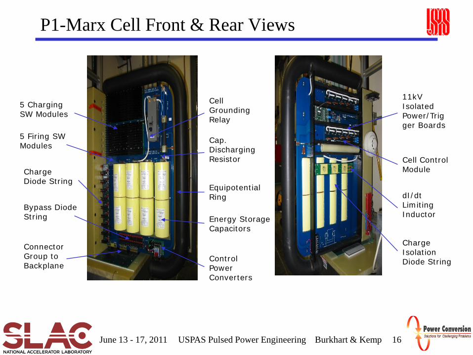
P1-Marx Cell Front & Rear Views
5 Charging SW Modules
5 Firing SW Modules
Charge Diode String
Bypass Diode String
Connector Group to Backplane
Cell Grounding Relay
Cap. Discharging Resistor
Control Power Converters
Equipotential Ring
11kV Isolated Power/Trigger Boards
Cell Control Module
Charge Isolation Diode String
dI/dt Limiting InductorEnergy Storage
Capacitors
USPAS Pulsed Power Engineering Burkhart & Kemp

June 13 - 17, 2011 17
P1-Marx Installed in “Sealed” Enclosure
USPAS Pulsed Power Engineering Burkhart & Kemp

June 13 - 17, 2011 18
P1-Marx Voltage Regulation
USPAS Pulsed Power Engineering Burkhart & Kemp

June 13 - 17, 2011 USPAS Pulsed Power Engineering: TTU PPSC 19
Marx Variant: Inversion Generator

June 13 - 17, 2011 USPAS Pulsed Power Engineering: TTU PPSC 20
Marx Variant: Inversion Generator (cont.)

June 13 - 17, 2011 USPAS Pulsed Power Engineering: TTU PPSC 21
Marx-PFL Hybrid: Stacked Blumlein
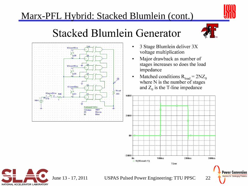
June 13 - 17, 2011 USPAS Pulsed Power Engineering: TTU PPSC 22
Marx-PFL Hybrid: Stacked Blumlein (cont.)

June 13 - 17, 2011 23
PFN Marx• Matched condition:
Zload= NZo
• PFN waveform sensitive to parasitic capacitance and inductance
• It does work!– 4 stage– 7 section PFN– Zo= 5 Ω
USPAS Pulsed Power Engineering Burkhart & Kemp

June 13 - 17, 2011 24
PFN Marx
USPAS Pulsed Power Engineering Burkhart & Kemp
June 13 - 17, 2011 25
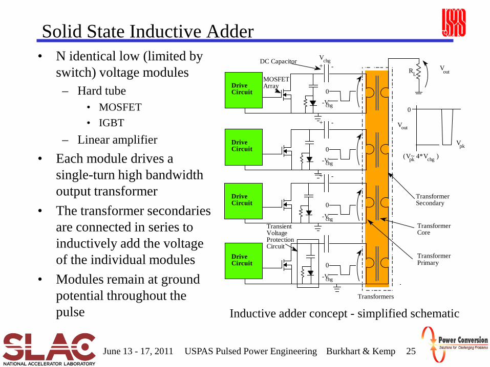
Solid State Inductive Adder
Drive Circuit
MOSFET Array
DC Capacitor+ -
0
-V chg
V chgVout
Transformer Secondary
+ -
+ -
( ~ 4* V chg )Vpk
0
Vpk
Vout
Transformers
Transformer Core
Transformer Primary
RL
Drive Circuit
Drive Circuit
Drive Circuit
0
-V chg
0
-V chg
0
-V chg
Transient Voltage Protection Circuit
Inductive adder concept - simplified schematic
• N identical low (limited by switch) voltage modules
– Hard tube• MOSFET• IGBT
– Linear amplifier• Each module drives a
single-turn high bandwidth output transformer
• The transformer secondaries are connected in series to inductively add the voltage of the individual modules
• Modules remain at ground potential throughout the pulse
USPAS Pulsed Power Engineering Burkhart & Kemp

June 13 - 17, 2011 26
Inductive Adder Topology - Advantages• All drive components ground referenced
• No high voltage grading required (except transformer secondary)
• Pulse format defined by programmable pulse generator
– Pulse width agility
– Burst frequency agility
– High burst frequency >1 MHz
• Modular - adder consists of stack of identical modules
– All modules switch same voltage/current
– All modules triggered simultaneously
– Scaleable to higher voltages by adding modules
• Low source impedance
– Can drive wide range of load impedance
– Load voltage is essentially independent of load
USPAS Pulsed Power Engineering Burkhart & Kemp

June 13 - 17, 2011 27
Inductive Adder Topology - Issues• Each module must switch full load current
– May require many parallel components (switches, capacitors, etc.)
– Parallel switching devices must have low jitter on both turn-on and turn-off
• Requires very low inductance in primary circuit
• Requires very fast opening switch that can interrupt full load current and survive fault currents
• Fault currents can be very large
• Cost
• Complexity
USPAS Pulsed Power Engineering Burkhart & Kemp

June 13 - 17, 2011 28
Inductive Adder Design Considerations• Select Switch and switch drive circuit
– Switching speed for both turn-on and turn-off– Maximum operating voltage (determines number of modules)– Current Rating (determines number of parallel devices)
• Size the capacitor (bank)– Must be large enough to meet droop requirements – Inductance must be low– Low ESR (equivalent series resistance)
• Design the pulse transformer– Core area must be sufficient for application
• Total volt-seconds for single pulse if reset between pulses• Total volt-seconds for all pulses in burst if reset between bursts
USPAS Pulsed Power Engineering Burkhart & Kemp

June 13 - 17, 2011 29
Inductive Adder Design Considerations• Make sure that primary circuit inductance is minimized
– Voltage drop across loop inductance during high di/dt affects load voltage– Energy stored in loop inductance can appear as voltage across switch – Include component inductance, transformer leakage inductance, and
inductance of circuit board traces• Protection circuits for switches
– Overvoltage from (L dI/dt)primary on turn off– Overcurrent; load faults, transformer saturation
• Reset of adder magnetic core– Duty cycle sets minimum ratio for Vreset/Voutput (total Vτ = 0)
• Recharge of capacitor between pulses/bursts – Interpulse recharge can reset core if voltage and current high enough
USPAS Pulsed Power Engineering Burkhart & Kemp
June 13 - 17, 2011 30
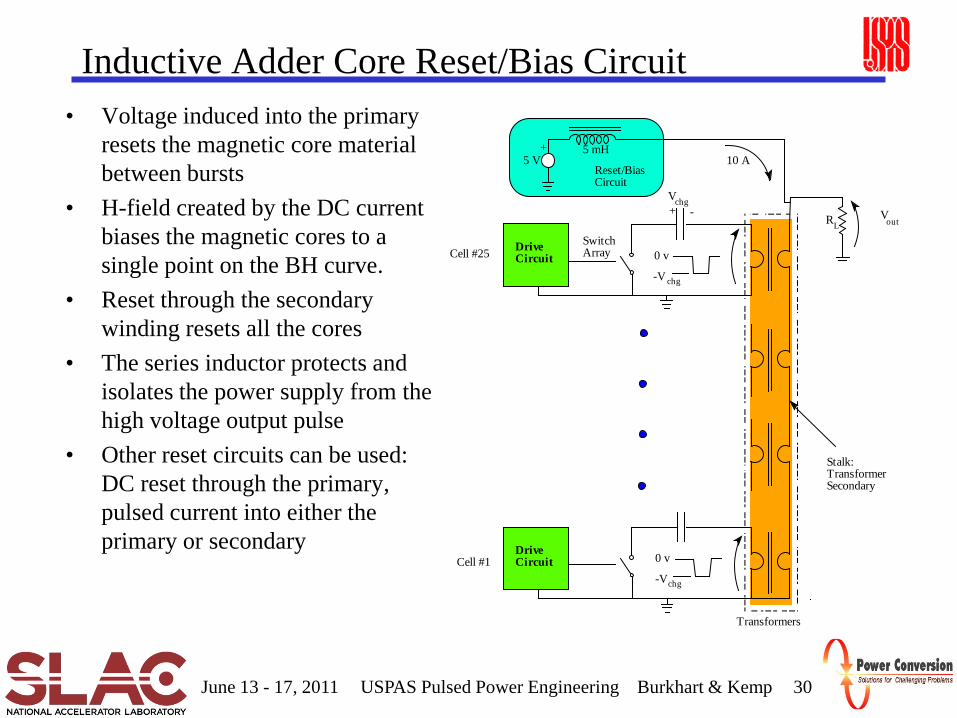
Inductive Adder Core Reset/Bias Circuit• Voltage induced into the primary
resets the magnetic core material between bursts
• H-field created by the DC current biases the magnetic cores to a single point on the BH curve.
• Reset through the secondary winding resets all the cores
• The series inductor protects and isolates the power supply from the high voltage output pulse
• Other reset circuits can be used: DC reset through the primary, pulsed current into either the primary or secondary
Drive Circuit
Switch Array
+ -
0 v
-V chg
V chgV
out
Stalk: Transformer Secondary
Transformers
0 v
-V chg
RL
Drive Circuit
+ 10 A
Reset/Bias Circuit
5 mH5 V
Cell #1
Cell #25
USPAS Pulsed Power Engineering Burkhart & Kemp
June 13 - 17, 2011 31
NLC Solid-State Inductive Adder Modulator• Modulator Requirements:
– Output Voltage 500kV @ 2kA– Pulse-width - 3µs– Klystron Efficiency > 80% (rise & fall times less than 400 ns)– Repetition Rate - 120 Hz (500kW Average)– Lifetime - 30 years– Cost < 200k$/ Modulator– Each modulator drives 8 klystrons
USPAS Pulsed Power Engineering Burkhart & Kemp

June 13 - 17, 2011 32
NLC Solid-State Inductive Adder Modulator• Fractional turn pulse transformer multiple parallel primaries, each
ground referenced– 500 kV, 2080 A, 1040 MW, 3.2µs, 500 kW average – 76 single turn primaries – Low loss Metglas cores– 3 turn secondary connects all cores in series– 152 IGBT switches (two per primary)
• Rating: 3.3 kV, 800 A rms• Operating point: 2.2 kV, 3.2 kA
• Major concerns– Klystron protection when there are internal faults– IGBT protection when load faults (requires active sense and control
circuitry)
USPAS Pulsed Power Engineering Burkhart & Kemp

June 13 - 17, 2011 33
IGBT Drivers and Core
Ground
core
USPAS Pulsed Power Engineering Burkhart & Kemp

June 13 - 17, 2011 34
Prototype NLC Solid State Induction Modulator
With oil tank installed
3 turn Secondary with water load
USPAS Pulsed Power Engineering Burkhart & Kemp

June 13 - 17, 2011 35
Prototype NLC Solid State Induction Modulator
• Coaxial Three Turn Secondary End Connection
USPAS Pulsed Power Engineering Burkhart & Kemp

June 13 - 17, 2011 36
Prototype NLC Induction Modulator Pulse (Water Load)
Three Turn Secondary76 Metglas cores152 IGBT Drivers
USPAS Pulsed Power Engineering Burkhart & Kemp

June 13 - 17, 2011 37
Comparison: Voltage Pulse of Induction Modulator vs. PFN
Nominal voltage: 350 kVPFN: 375 AAdder: 750 AOverall adder efficiency >80%
USPAS Pulsed Power Engineering Burkhart & Kemp

June 13 - 17, 2011 38
2-Pack Adder Cell w/Drive Boards (with 6.5kV IGBTs)
USPAS Pulsed Power Engineering Burkhart & Kemp
June 13 - 17, 2011 39
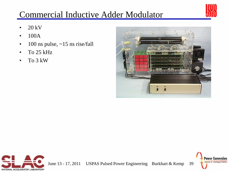
Commercial Inductive Adder Modulator• 20 kV• 100A• 100 ns pulse, ~15 ns rise/fall• To 25 kHz• To 3 kW
USPAS Pulsed Power Engineering Burkhart & Kemp

June 13 - 17, 2011 40
Transformation: Inductive to Transmission Line Adder (D Birx)
USPAS Pulsed Power Engineering Burkhart & Kemp

June 13 - 17, 2011 41
10 Ω 15 Ω 20 Ω45 Ω 50 Ω
Pulse Card 50V → 5Ω
Pulse Card 50V → 5Ω
Pulse Card 50V → 5Ω
Pulse Card 50V → 5Ω
Pulse Card 50V → 5Ω
Pulse Card 50V → 5Ω
Pulse Card 50V → 5Ω
Pulse Card 50V → 5Ω
Pulse Card 50V → 5Ω
Pulse Card 50V → 5Ω
10 floating Pulse cards, 50 V→5Ω5Ω output
is two10Ω coax in parallel
Each pulse card has 5 FETS, each fet
drives 25 Ω
Output:
500V→50Ω
ferrite combiner
Transmission Line Adder Scheme: Cartoon
HINS Chopper: FNAL
USPAS Pulsed Power Engineering Burkhart & Kemp
June 13 - 17, 2011 42
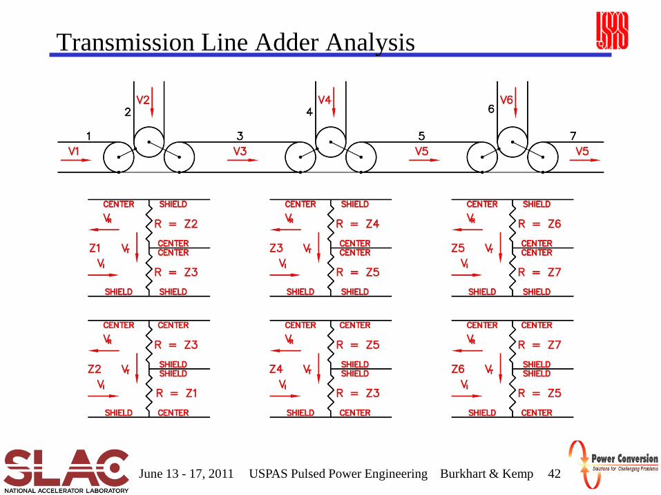
Transmission Line Adder Analysis
USPAS Pulsed Power Engineering Burkhart & Kemp

June 13 - 17, 2011 43
Transmission Line Adder Analysis (cont.)• Transmitted wave: VT/VI = (2 R) / (R + ZO)• Reflected wave: VR/VI = [(R - ZO) / (R + ZO)]• Junction of lines 1, 2, & 3
– (VT/VI )1 = (VT/VI )2 = (2)(15)/(15 + 5) = 3/2• Of the wave transmitted from 1: 1/3 → 2 and 2/3 → 3 by resistive division• Of the wave transmitted from 2: 1/3 → 1 and 2/3 → 3 by resistive division
– (VR/VI )1 = (VR/VI )2 = (15 - 5)/(15 + 5) = 1/2– Line 1: VR = VR1 - (1/3)VT2 (center to shield) = VI1/2 - (1/3)(3VI2/2) = 0
if lines 1 and 2 carry the same waveform – Line 2: VR = VR2 - (1/3)VT1 (shield to center) = VI2/2 - (1/3)(3VI1/2) = 0 – Line 3: VI = (2/3)VT1 + (2/3)VT2 = (1/3)(3VI1/2) + (1/3)(3VI2/2) = VI1 + VI2
USPAS Pulsed Power Engineering Burkhart & Kemp

June 13 - 17, 2011 44
Transmission Line Adder Analysis (cont.)• Junction of lines 3, 4, & 5
– (VT/VI )3 = (2)(5 + 15)/(5 + 15 + 10) = 4/3• Of the wave transmitted from 3: 1/4 → 4 and 3/4 → 5 by resistive division
– (VT/VI )4 = (2)(15 + 10)/(15 + 10 + 5) = 5/3• Of the wave transmitted from 4: 2/5 → 3 and 3/5 → 5 by resistive division
– (VR/VI )3 = (20 - 10)/(20 + 10) = 1/3– (VR/VI )4 = (25 - 5)/(25 + 5) = 2/3– Line 3: VR = VR3 - (2/5)VT4 (center to shield) = VI1/3 - (2/5)(5VI4/3) = 0
if line 3 carries a waveform that is 2X of line 4– Line 4: VR = VR4 - (1/4)VT3 (shield to center) = 2VI4/3 - (1/4)(4VI3/3) = 0 – Line 5: VI = (3/4)VT3 + (3/5)VT4 = (3/4)(4VI3/3) + (3/5)(5VI5/3) = VI3 + VI4
USPAS Pulsed Power Engineering Burkhart & Kemp

June 13 - 17, 2011 45
Transmission Line Adder Analysis (cont.)• Junction of lines 5, 6, & 7
– (VT/VI )5 = (2)(25)/(25 + 15) = 5/4• Of the wave transmitted from 5: 1/5 → 6 and 4/5 → 7 by resistive division
– (VT/VI )6 = (2)(35)/(35 + 5) = 7/4• Of the wave transmitted from 6: 3/7 → 5 and 4/7 → 7 by resistive division
– (VR/VI )5 = (25 - 15)/(25 + 15) = 1/4– (VR/VI )6 = (35 - 5)/(35 + 5) = 3/4– Line 5: VR = VR5 - (3/7)VT6 (center to shield) = VI5/4 - (3/7)(7VI6/4) = 0
if line 5 carries a waveform that is 3X of line 6– Line 6: VR = VR6 - (1/5)VT5 (shield to center) = 3VI6/4 - (1/5)(5VI5/4) = 0 – Line 7: VI = (4/5)VT3 + (4/7)VT4 = (4/5)(5VI5/4) + (4/7)(7VI6/4) = VI5 + VI6
•••
USPAS Pulsed Power Engineering Burkhart & Kemp

June 13 - 17, 2011 46
Where TL Adder & Blumlein Collide: Sparktronics Multi-stage Blumlein
USPAS Pulsed Power Engineering Burkhart & Kemp

June 13 - 17, 2011 47
Resonant Converter-Modulator• Switch-mode converter
– Chopping at solid state switch voltage– AC transformer steps up to high voltage– High frequency inverter
• Minimizes transformer size• Minimizes output filter size• Minimizes output pulse risetime
• Poly-phase for high power• Resonant circuit
– Transformer leakage inductance → high voltage– Tuning capacitor
• Rectification• Filtering
– Inductive– HF trap
(I/O)(FEEDBACK)
RECTIFIER TRANSFORMERAND FILTERS
SCRREGULATOR
ENERGYSTORAGE/SWITCHI
NG
BOOST TRANSFORMER
HV RECTIFIERAND FILTER NETWORK
INPUTLINE CHOKE
5th
HARMONICTRAP
7th
HARMONICTRAP
13.8KV3Ø
50mH
AØ
BØCØ3Ø
(ON/OFF)
4mH400A
4mH400A
6 EACH
6 EACH
RTN
X3
CSHUNT-PEAK
AØ BØ CØ
-HV -HV -HV 10ohm 20mH
.03uF
.03uF.05uF VMON
HVOUTPUT
EQUIPMENTCONTROL
RACK
USPAS Pulsed Power Engineering Burkhart & Kemp

June 13 - 17, 2011 48
Spallation Neutron Source: High Voltage Converter Modulator (HVCM)• Three-phase resonant converter modulator• Primary power: ±1.25 kV
– Compatible with HV IGBT modules– Air insulation, simplifies maintenance
• Resonant transformer– Inductance for switching circuit (zero-current switching)– Added voltage gain– Resonant circuit impedance tuned to load power needs
• 2X voltage multiplier after rectification• Filtering to meet klystron regulation requirements• Output
– Average power: to 1 MW– Peak power: to 11 MW– Output voltage: 70 – 125 kV– Pulse length: 1.1 to 1.6 ms– PRF: to 60 Hz
USPAS Pulsed Power Engineering Burkhart & Kemp

June 13 - 17, 2011 49
SNS HVCM• 20 kHz inverter frequency
– Small transformers– Small output filter
• Fast risetime (~100 μs)• Low stored energy: minimize arc fault energy
• Low inverter voltage (~2 kV)– H-bridge is air insulated– Only low maintenance HV components are in oil
• The resonant peaking capacitors allow fault “ride-through” capabilities. – Load impedance changes (such as klystron discharges) de-tune the resonant circuit.– Down-side, resonant circuit tuning sensitive to changes in load (klystron
perveance)• Modulator was designed for PWM operation to obtain a well-regulated output
pulse
USPAS Pulsed Power Engineering Burkhart & Kemp

June 13 - 17, 2011 50
SNS HVCM (Tuned for SLAC L-band)
Output voltage waveform Primary current waveforms
USPAS Pulsed Power Engineering Burkhart & Kemp

June 13 - 17, 2011 51
SNS HVCM
DC Storage Capacitors
Three H-bridge Switch Plates
High-Voltage Oil Tank
HV basket located inside oil tank
USPAS Pulsed Power Engineering Burkhart & Kemp
June 13 - 17, 2011 52
Magnetic Pulse Compression Circuits• Magnetic Circuit/Systems
– Basics– Relevant Equations– Limitations– Other Practical Consideration– Mechanical Design– Examples of Operational Systems– References
USPAS Pulsed Power Engineering Burkhart & Kemp

June 13 - 17, 2011 53
Magnetic Switch Principles• A magnetic switch is a device, usually constructed as a winding around
a magnetic core, that uses the non-linear properties of magnetic materials to achieve a large change in impedance
• The impedance of a magnetic switch varies from a large inductance (high permeability when magnetic core unsaturated) to a small inductance (low permeability when magnetic core saturated)
Note: With few exceptions a magnetic switch needs a “real” switch somewhere in the circuit ahead of the magnetic switch to initiate magnetic compression . This real switch will need to be capable of handling the same energy as the magnetic switch but at much lower peak power levels.
USPAS Pulsed Power Engineering Burkhart & Kemp

June 13 - 17, 2011 USPAS Pulsed Power Engineering: E Cook 54
Definition of TermsTerm Definition Units
Ln the nth stage of ma gnetic comp ressionVoln minim um magnet ic core volum e of Ln meters3
An magnetic cross-sectional area of Ln meters2
OD outer diameter of magnetic core (toroid) metersID inn er diameter of magnetic core (toroid) meters² Bs usable chan ge in core flux densi ty teslaNn num ber of tu rns on the Ln wind ingwn axial length of Ln wind ing meters² r rad ial thickness of magnet ic core meters
<r> mean radi us of ma gnetic core meterspf pac ki ng facto r - cross-section area of ma gnetic mater ial
div ided by t otal area encl osed by windings
Lnsat satura ted inductanc e of Ln henriesGainn rat io of cha rge to discharge time for Ln
Cn capac itan ce at the inp ut of Ln faradsECn per pu lse energy stored on Cn joules
<VCn> av erage charge voltage on capa citor Cn voltsτCnchg time requ ired for capac itor Cn to cha rge to peak vol tage secondsτLn sat hold-off time - time requ ired t o satu rate Ln at a given
av erage charge voltageseconds
tprop total p ropagat ion delay through the mo dulator - equal tothe sum of the hold-off t imes of all the stages
seconds
µo free spac e permeability = 4š*10-7 henries/mµr relative permeability
µrsat satura ted value of relat ive permeabili ty<µrsat> av erage relative permeability du ri ng saturati on
² t time jitter seconds² v pu lse-to-pu lse vari at ions in peak charge voltage volts

June 13 - 17, 2011 USPAS Pulsed Power Engineering: E Cook 55
Magnetic Switch Operation

June 13 - 17, 2011 USPAS Pulsed Power Engineering: E Cook 56
Basic Compression Circuit Equations
C C Cn-1 n n+1
Ln-1 Ln
τCn
chg = π Ln−1sat Ceq = π Ln −1
sat Cn
2
τCn
chg ≈ τLnsat =
NnAn∆Bs
< VCn>
Cn − 1 = Cn = Cn + 1where:
The resonant charging voltage waveshape of this circuit has the form:And for this waveshape <VCn> is equal toVpk/2 when integrated to the time of peak voltage.
Combining the equations (1) and (2) and solving for Ln-1
sat gives:
Where ECn is the peak energy stored in Cn
V(t) =Vpk2
(1 − cos(ωt))
Ln−1
sat =
2N nAn∆Bs
π
2
12 CnVpk
2 =
2N nAn∆Bs
π
2
ECn
(1)
(2)
(3)
June 13 - 17, 2011 USPAS Pulsed Power Engineering: E Cook 57
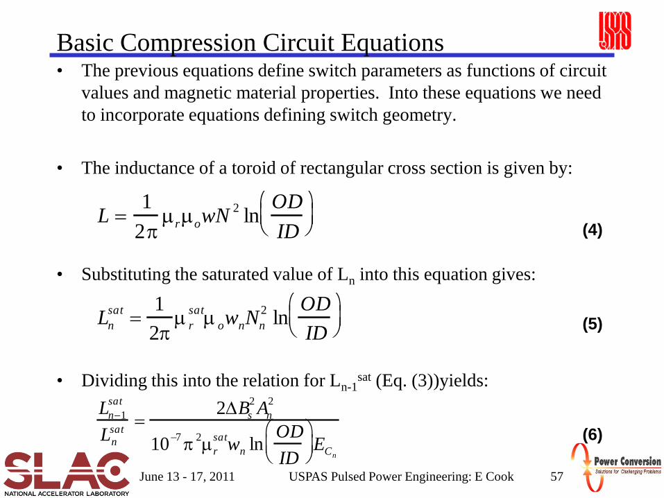
Basic Compression Circuit Equations• The previous equations define switch parameters as functions of circuit
values and magnetic material properties. Into these equations we need to incorporate equations defining switch geometry.
• The inductance of a toroid of rectangular cross section is given by:
• Substituting the saturated value of Ln into this equation gives:
• Dividing this into the relation for Ln-1sat (Eq. (3))yields:
Lnsat =
12π
µ rsatµ ownNn
2 lnODID
L =1
2πµr µowN 2 ln
ODID
Ln−1sat
Lnsat =
2∆Bs2 An
2
10−7 π 2µrsatwn ln
ODID
ECn
(4)
(5)
(6)

June 13 - 17, 2011 USPAS Pulsed Power Engineering: E Cook 58
Basic Compression Circuit Equations• However:
• and therefore:
• Using the expansion for the natural log term: w ln(OD/ID) ≈ w ∆r/<r> = An/<r>
• Dividing eq. (3 ) by (9) and rearranging gives:
Ln−1sat
Lnsat =
τCn
chg
τCn+1
chg
2
= Gainn2
Gainn2 =
2∆Bs2An
2
10−7 π2µ rsatwn ln
ODID
ECn
Voln ≈
Gainn2ECn
π 2µ rsatµo
4∆Bs2
Lnsat ≈
µrsatµ oNn
2 An
2π < r >=
µ rsatµo Nn
2 An2
Voln
(7)
(8)
(9)
(10)

June 13 - 17, 2011 USPAS Pulsed Power Engineering: E Cook 59
Basic Compression Circuit Equations• Voln in Eq. (10) represents the minimum volume of magnetic material
(and therefore minimum loss) required for a switch, Ln, given a required gain, per pulse energy, and ∆Bs. Eq. (10) assumes that the entire toroidal volume inside the winding is filled with magnetic material. This is never achieved in practice and the term packing factor (pf) is defined:
Voln ≈Gainn
2ECnπ2µr
satµ o
pf4∆Bs2
pf = the cross-section area of magnetic material divided by the total area enclosed by the windings
This modifies the minimum volume equation to the following:

June 13 - 17, 2011 USPAS Pulsed Power Engineering: E Cook 60
Magnetic Compression Circuits
• To achieve higher overall gain, multiple switches may be used– Switches are designed to saturate sequentially– Multiplying individual switch gains yields the overall gain
• Capabilities of magnetic compression systems– High repetition rate– High average power– Very high peak power– High reliability
• Note: A “real” switch (one than can be controlled by external trigger is required to initiate the magnetic compression sequence
L1 L2 L3
C1 C2 C3 C4

June 13 - 17, 2011 USPAS Pulsed Power Engineering: E Cook 61
Magnetic System Limitations- Jitter • Time Jitter - caused by variations of voltage and ∆B as per:
– Jitter is proportional to the total propagation delay through the magnetic system (sum of the individual switch hold-off times)
• Example: If the total propagation delay is 10µs and the average input voltage variation is 1% the minimum time jitter (∆B variation is zero) is:
– ∆t ~ 10µs*.01 = 100ns– Jitter can be minimized by:
• Precisely resetting the magnetic cores prior to the next pulse• Precise voltage regulation or real-time adjustment of trigger pulse to
compensate for ∆V
• Jitter of < ± 2ns can be reasonably anticipated for systems having propagation delays < 10 µs
τCn
chg ≈ τLnsat =
NnAn∆Bs
< VCn>

June 13 - 17, 2011 USPAS Pulsed Power Engineering: E Cook 62
Magnetic System Limitations - Risetime & Repetition Rate• Risetime: the pulse risetime is determined by the saturated inductance of the
winding geometry. It is possible to obtain single turn inductance in the nH range. In practice, output risetimes in the range of 10-20 ns are routinely achieved for high voltage systems
• Repetition Rates:– Burst Repetition Rate
• Parallel systems (Branch Magnetics) can operate at 10’s of MHz• Single pass systems can probably work up to ~ 100 kHz (the limitation is that all the
magnetic cores need to be reset between pulses– Constant Repetition Rate
• Single pass systems can operate into the 10-20 kHz region (liquid cooling is required to remove heat generated in the magnetic cores and capacitors)
– Metglas™ is limited to < 5 kHz for the fastest saturation rates (output stages) but may easily be used for earlier stages. Another limitation of Metglas™ at fast saturation rates (high ∆B/∆t) is voltage breakdown between laminations
– Ferrites are often used for the output stages in high rep-rate systems

June 13 - 17, 2011 USPAS Pulsed Power Engineering: E Cook 63
Magnetic System Limitations - Number of Stages• The total gain required by the system determines the number of stages
where the total gain in the product of the individual switch gains– Individual switch gain is restricted by the core volume relationship:
• Maximum reasonable core gain:– ~ 3 for ferrite– 5-10 for Metglas™ and other amorphous materials
• When more than two switches are required, a step-up transformer is normally needed (eliminates trying to design fractional turn switches)
• Usually only 3 magnetic switches are required to cover the range of microseconds (initial conduction time) to nanoseconds (output risetime)
Voln ≈
Gainn2ECn
π 2µ rsatµo
4∆Bs2

June 13 - 17, 2011 USPAS Pulsed Power Engineering: E Cook 64
Other Practical Considerations - µrsat
• Saturated permeability - The assumption is that the saturated inductance of a magnetic switch may be calculated by assuming that µr has the value of unity (free space). While this is a valid assumption when the H field is high enough, empirical data indicated that surprisingly large values of ampere turns are required to fully saturate a magnetic core. The net effect is that during the time of saturation and energy transfer through the magnetic switch the average value of saturated permeability should be considered as having a value somewhere between 1 and 2. The actual value will be dependent on the magnetic core material chosen and the geometry of the winding around the core.
0 10 20 30 41
2
3
4
5
H-Field (kA/m)
y = 5.3978 * x^-0.4038 R = 0.87
Rat io of Ind uctanc e Values versus Peak H-Field (Ferr ite Core)
This curve is generated by allowing a magnetic switch to ring in a resonant, low loss circuit. The average saturated inductance (calculated from the peak current of the oscillations) is divided the calculated air core inductance for µr = 1 and plotted versus the peak H-field corresponding to each value of peak current. Note that the inductance ratio levels out at ~ 1.5 for a peak field of~ 25kA/m: this indicates that the core is fully saturated and that the winding geometry is responsible for the measured inductance being higher than the calculated value.

June 13 - 17, 2011 USPAS Pulsed Power Engineering: E Cook 65
Other Practical Considerations - Reset/BiasReset/Bias - Achieving consistent performance from a magnetic switch requires that the initial state of the magnetic core be known and the easiest way to know the initial condition of the magnetic is to force it to a known position. This is usually the task of the reset/bias circuit. The magnetic cores must first be reset - in essence the volt-seconds used by the switch must be replaced by voltage applied of the opposite polarity such that the volt-second product is equal to or greater than that used during the initial energy compression. The cores can be reset
B
H
Bsat
-Br
Bias
²B ²B
by voltage applied to the main windings or to a turn through the core that is not part of the pulse power circuit (in essence a secondary winding as the magnetic switch will function as a transformer until the core material is again saturated). In either case the reset circuit must be protected/isolated from the high-voltage pulses generated during normal operation. Isolation is usually achieved by using large inductors although diode isolation can be used. DC bias is used to hold the magnetic core at a particular point on the BH curve and provides the additional benefit of increasing the useable ∆B for a given core. Note the polarity of the bias current is opposite the switch discharge current.
June 13 - 17, 2011 66
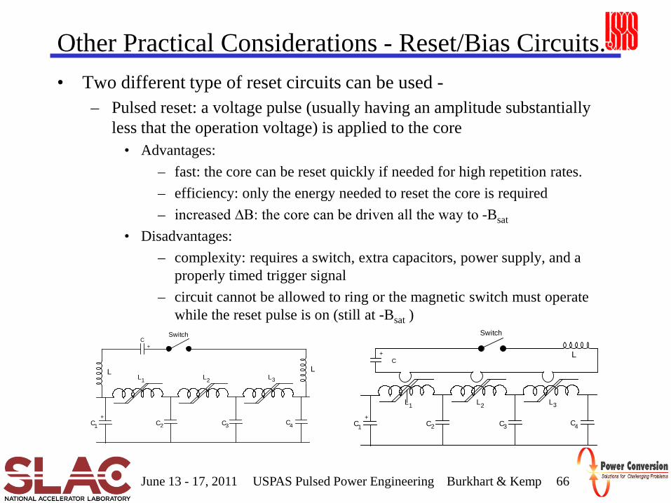
Other Practical Considerations - Reset/Bias Circuits.• Two different type of reset circuits can be used -
– Pulsed reset: a voltage pulse (usually having an amplitude substantially less that the operation voltage) is applied to the core
• Advantages: – fast: the core can be reset quickly if needed for high repetition rates. – efficiency: only the energy needed to reset the core is required– increased ∆B: the core can be driven all the way to -Bsat
• Disadvantages: – complexity: requires a switch, extra capacitors, power supply, and a
properly timed trigger signal– circuit cannot be allowed to ring or the magnetic switch must operate
while the reset pulse is on (still at -Bsat ) Switch
LL
C+
L1 L2 L3
C1 C2 C3 C4+ +
L1 L2 L3
C1 C2 C3 C4
Switch
LC
+
USPAS Pulsed Power Engineering Burkhart & Kemp

June 13 - 17, 2011 67
Other Practical Considerations - Reset/Bias Circuits– DC reset: a low voltage DC power supply is connected to the magnetic
switch through an large inductor (compared to the pulse duration) thereby creating a current source
• Advantages:– simplicity: few components and no timing requirements– inexpensive: components not costly– reliability: not much to break– Increased ∆B: the DC reset also serves as a DC bias
• Disadvantages:– efficiency: the power supply is usually on all the time
BV
+
L1 L2 L3
C1 C2 C3 C4
L+
LBV
+
L1 L2 L3
C1 C2 C3 C4
L+
USPAS Pulsed Power Engineering Burkhart & Kemp

June 13 - 17, 2011 68
Mechanical Design• The mechanical design of a magnetic switch is more complicated than
the electrical portion of the design.• The mechanical is guided by two contradictory requirements:
– the need to minimize inductance of the winding structure (including connections to capacitors and other switches) in order to optimize the performance of the magnetic switch
– the need to ensure reliable performance of a winding structure that must operate at high voltage
• In addition, the mechanical design must have sufficient mechanical robustness to adequately support the magnetic material (which may have substantial weight) and ensure that the position of the windings is controlled and the inductance of the mechanical structure is fixed and repeatable (particularly if production quantities are envisioned).
– In general, turns of wire around a core are not going to meet these requirements.
USPAS Pulsed Power Engineering Burkhart & Kemp

June 13 - 17, 2011 69
Mechanical Design• A common method of constructing a magnetic switch on a toroidal
core of rectangular cross-section is to use metal rods on the inside diameter (ID) and outside diameter (OD). Crossover links on the ends of the switch may be fabricated with metal bars or may be attached to a printed circuit board.
– For calculation of the inductance use the dimensions to the middle of the rods (for ID and OD)
– When only a few turns are needed, use multiple sets of windings to enclose the core as completely as possible.
– When using nickel-zinc ferrite (high intrinsic resistance),the turns can be touching the core
– Connections between the magnetic switch and capacitors should be as short and wide (such as a parallel plate layout) as possible to minimize inductance
– The spacing between conductors at high voltage should be adequate to prevent electrical breakdown and all edges of high voltage conductors should have as large a radius as possible in order to reduce field enhancement
USPAS Pulsed Power Engineering Burkhart & Kemp

June 13 - 17, 2011 USPAS Pulsed Power Engineering: E Cook 70
Mechanical Design - Example
5 -Turn Switch (configured as 4 sets of 5 turns)
20kV hold-off for 1µs with gain of 3.0 using ferrite toroids.
Inside and outside turns are fabricated of 0.375” Dia. rod.
Crossover connections between inside and outside rods are patterns on printed circuit boards. Board pattern on top and bottom boards are different.
Output connections: each common to two windings
Input connections: each common to two windings
1 2 3 45
34
21
2
23
3
4
45

June 13 - 17, 2011 USPAS Pulsed Power Engineering: E Cook 71
Mechanical Design - Example• When only one or two turns are required, tubes and concentric tubes
can be used as the turns through the center of the core– Remember that the current return on the outside of the core needs to close
to the core to minimize the inductanceAB
CD
Cap
Cap
Cap
Cap
D
Ferrite ToroidsCenter Line
Cap
Lsw
A
B
C
DLsw
Electrical Schematic
Cross-section of 2-turn magnetic switch with turns split as shown in the schematic. This approach is used to reduce maximum field stress to ground by operating at positive and negative input voltages with respect to ground.
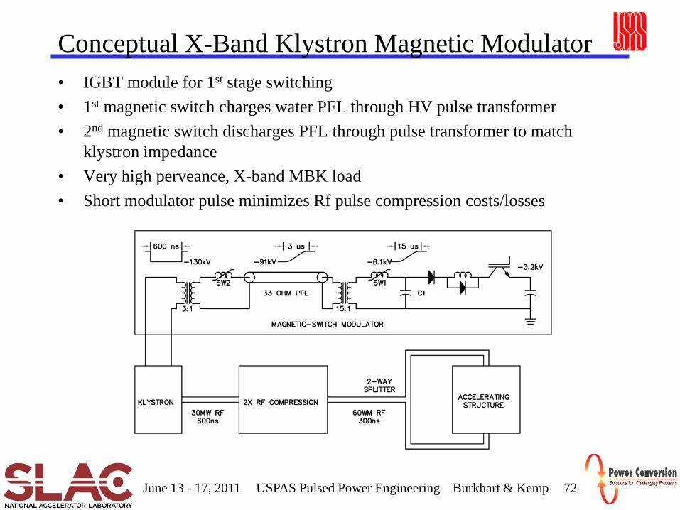
June 13 - 17, 2011 72
Conceptual X-Band Klystron Magnetic Modulator• IGBT module for 1st stage switching• 1st magnetic switch charges water PFL through HV pulse transformer• 2nd magnetic switch discharges PFL through pulse transformer to match
klystron impedance• Very high perveance, X-band MBK load• Short modulator pulse minimizes Rf pulse compression costs/losses
USPAS Pulsed Power Engineering Burkhart & Kemp

June 13 - 17, 2011 73
8-Pulse Demonstration Generator [Branch Magnetics] 35MHz - Maximum Burst Frequency
Firing Sequence - CR1, CR3, CR5, CR7, CR2, CR4, CR6, AND CR8
USPAS Pulsed Power Engineering Burkhart & Kemp

June 13 - 17, 2011 74
Ultra-fast DSRD Switched TL Modulator
• DSRD as a sub-ns opening switch for a transmission line modulator for the ILC damping ring kickers
– 5 kV into 50 Ω– 4 ns flattop, <1 ns rise/fall (simulations for 2 ns pulse)– Bunch separation <10 ns– 3 (or 6) MHz burst at 5 Hz
• Switch, SW, is closed to charge L1, some parasitic component is transferred through C1/T1 for forward bias D1
• SW opens, L1 discharges into T1 via C1 (resonant transfer), D1 is still in conduction (reverse recovery charge), shorting T1 (current charging of T1 inductance)
• Energy transfer from L1 to T1 is completed as D1 opens• T1 now connected to matched load, R1
USPAS Pulsed Power Engineering Burkhart & Kemp

June 13 - 17, 2011 75
DSRD Modulator Energy Transfer Sequence
• Voltage (left) and current of L1 during charging period (SW closed)
USPAS Pulsed Power Engineering Burkhart & Kemp

June 13 - 17, 2011 76
DSRD Modulator Energy Transfer Sequence (cont)
(a): Current in L1 (green) and C2 (yellow) during charging of L1 (t<154 ns) and transfer to T1
(b): Detail of C2 current during energy transfer to T1 (t<170.5 ns) and discharge into load, note current through C2 until halfway through T2 discharge (t=171.5 ns)
(c): D1 current (green) and T1 current, load end, (yellow)
(a) (b)
(c)
USPAS Pulsed Power Engineering Burkhart & Kemp

June 13 - 17, 2011 77
DSRD Modulator Energy Transfer Sequence (cont)
• Detail of D1 current (green) and T1 current, load end, (yellow) during transfer of energy to load (above right)
• Load current during discharge of T1 (above left)• Challenges
– Pre-pulse: finite DSRD turn-on time and forward-voltage– Post-pulse: residual energy will “bounce around” and come out at later time– Optimum timing dependent on precise DSRD properties that depend are
temperature dependent
USPAS Pulsed Power Engineering Burkhart & Kemp


