
Article Number: PDS ALC0100-2X00 Prepared: PBDocument Date: 2010-11-16 Verified: MCCurrent Revision no.: G Approved: MCCurrent Revision Date: 2014-02-13 Page Number: 1 of 24
PRODUCT SPECIFICATIONAUDIO LINE COMBINATION
ALC0100-2X00
SCOPE
These technical specifications describes the functionalities and features of the AnaviewAudio Line Combination ALC0100-2500, an integrated audio solution combining high-endamplifier and power supply technology, capable of delivering 2x50W into 4Ω @1%THD, 2x25W into 8Ω @1%THD or 1x100W into 8Ω bridged. Instantaneous peak power 170W BTL 6Ω. Typical applications are audio receivers, powered speakers and residential audio system.
The ALC0100 exists in four models;ALC0100-2200: Without standby converter, DISABLE function and hanger possibilityALC0100-2300: With standby converter and DISABLE function, without hanger possibiliyALC0100-2400: Without standby converter and DISABLE function, with hanger possibilityALC0100-2500: With standby converter, DISABLE function and hanger possibility

Article Number: PDS ALC0100-2X00 Prepared: PBDocument Date: 2010-11-16 Verified: MCCurrent Revision no.: G Approved: MCCurrent Revision Date: 2014-02-13 Page Number: 2 of 24
Disclaimer
The data sheet contains specifications that may be subject to change without priornotice. Responsibility for verifying the performance, safety, reliability andcompliance with legal standards of end products using this subassembly falls to themanufacturer of said end product.
ANAVIEW products are not authorized for use as critical components in life supportdevices or life support systems without the express written approval of the president ofETAL Group AB. As used herein:1. Life support devices or systems are devices or systems which, (a) are intended forsurgical implant into the body, or (b) support or sustain life, and whose failure to performwhen properly used in accordance with instructions for use provided in the labelling, canbe reasonably expected to result in a significant injury to the user.2. A critical component is any component of a life support device or system whose failureto perform can be reasonably expected to cause the failure of the life support device orsystem, or to affect its safety or effectiveness.
Article Number: PDS ALC0100-2X00 Prepared: PBDocument Date: 2010-11-16 Verified: MCCurrent Revision no.: G Approved: MCCurrent Revision Date: 2014-02-13 Page Number: 3 of 24
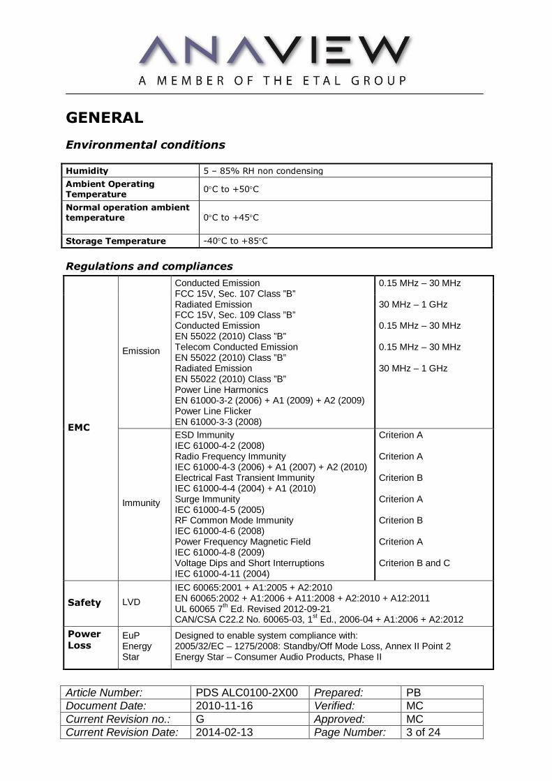
GENERAL
Environmental conditions
Humidity 5 – 85% RH non condensing
Ambient OperatingTemperature
0C to +50C
Normal operation ambienttemperature 0C to +45C
Storage Temperature -40C to +85C
Regulations and compliances
EMC
Emission
Conducted EmissionFCC 15V, Sec. 107 Class ”B”Radiated EmissionFCC 15V, Sec. 109 Class ”B”Conducted EmissionEN 55022 (2010) Class ”B”Telecom Conducted EmissionEN 55022 (2010) Class ”B”Radiated EmissionEN 55022 (2010) Class ”B”Power Line HarmonicsEN 61000-3-2 (2006) + A1 (2009) + A2 (2009)Power Line FlickerEN 61000-3-3 (2008)
0.15 MHz – 30 MHz
30 MHz – 1 GHz
0.15 MHz – 30 MHz
0.15 MHz – 30 MHz
30 MHz – 1 GHz
Immunity
ESD ImmunityIEC 61000-4-2 (2008)Radio Frequency ImmunityIEC 61000-4-3 (2006) + A1 (2007) + A2 (2010)Electrical Fast Transient ImmunityIEC 61000-4-4 (2004) + A1 (2010)Surge ImmunityIEC 61000-4-5 (2005)RF Common Mode ImmunityIEC 61000-4-6 (2008)Power Frequency Magnetic FieldIEC 61000-4-8 (2009)Voltage Dips and Short InterruptionsIEC 61000-4-11 (2004)
Criterion A
Criterion A
Criterion B
Criterion A
Criterion B
Criterion A
Criterion B and C
Safety LVD
IEC 60065:2001 + A1:2005 + A2:2010EN 60065:2002 + A1:2006 + A11:2008 + A2:2010 + A12:2011UL 60065 7
thEd. Revised 2012-09-21
CAN/CSA C22.2 No. 60065-03, 1st
Ed., 2006-04 + A1:2006 + A2:2012
PowerLoss
EuPEnergyStar
Designed to enable system compliance with:2005/32/EC – 1275/2008: Standby/Off Mode Loss, Annex II Point 2Energy Star – Consumer Audio Products, Phase II

Article Number: PDS ALC0100-2X00 Prepared: PBDocument Date: 2010-11-16 Verified: MCCurrent Revision no.: G Approved: MCCurrent Revision Date: 2014-02-13 Page Number: 4 of 24
Miscellaneous product specifications
Model selection chart
ModelStandby
Converter*
AcceptsHangerModule†
Application
ALC0100-2200 2-channel amplifier with ability to BTLfor mono applications
ALC0100-2300
2-channel amp with standby supply;meets Energy Star 2.0 and EuP
ALC0100-2400
2-channel amplifier with ability topower 3rd channel for 3 channel, 2.1systems and BTL + SE systems idealfor 2-way LF/HF active speakers.
ALC0100-2500
Full featured model with standbysupplies meeting Energy Star/EuP andability to power 3rd channel.
* Standby Converter Option - offers Aux V1 8V keep-alive supply, ability to place module instandby mode (i.e. DISABLE)† Hanger Module Option – offers Aux V4 and V5 high voltage rails to power an optional HangerModule amplifier channel.
Cooling Convection cooling
Mounting of the unit See Figure 1 Board outline, dimensions (page 10).
IEC Protection Class Class II - Double insulation
Efficiency 82% at 230Vac, 1kHz 2x50W into 4Ω
Idle power consumption 6W typ. (8W max) at 230VAC
Standby mode powerconsumption
<500mW typ. when remote shut down by DISABLE input anddelivering 20mA on V1.
Manufacturing according toworkmanship standard
IPC-A-610, Revision D, February 2005
Article Number: PDS ALC0100-2X00 Prepared: PBDocument Date: 2010-11-16 Verified: MCCurrent Revision no.: G Approved: MCCurrent Revision Date: 2014-02-13 Page Number: 5 of 24
ELECTRICAL SPECIFICATIONS
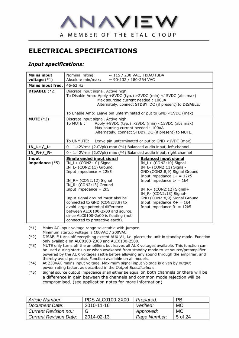
Input specifications:
Mains inputvoltage (*1)
Nominal rating: ~ 115 / 230 VAC, TBDA/TBDAAbsolute min/max: ~ 90-132 / 180-264 VAC
Mains input freq. 45-63 Hz
DISABLE (*2) Discrete input signal. Active high.To Disable Amp: Apply +8VDC (typ.) >2VDC (min) <15VDC (abs max)
Max sourcing current needed : 100uAAlternately, connect STDBY_DC (if present) to DISABLE.
To Enable Amp: Leave pin unterminated or put to GND <1VDC (max)
MUTE (*3) Discrete input signal. Active high.To MUTE : Apply +8VDC (typ.) >2VDC (min) <15VDC (abs max)
Max sourcing current needed : 100uAAlternately, connect STDBY_DC (if present) to MUTE.
To UNMUTE: Leave pin unterminated or put to GND <1VDC (max)
IN_L+/_L- 0 - 1.42Vrms (2.0Vpk) max (*4) Balanced audio input, left channel
IN_R+/_R- 0 - 1.42Vrms (2.0Vpk) max (*4) Balanced audio input, right channel
Inputimpedance (*5)
Single ended input signalIN_L+ (CON2:10) SignalIN_L- (CON2:11) GroundInput impedance = 12k5
IN_R+ (CON2:12) SignalIN_R- (CON2:13) GroundInput impedance = 2k5
Input signal ground must also beconnected to GND (CON2:8,9) toavoid large potential differencebetween ALC0100-2x00 and source,since ALC0100-2x00 is floating (notconnected to protective earth).
Balanced input signalIN_L+ (CON2:10) Signal+IN_L- (CON2:11) Signal-GND (CON2:8,9) Signal GroundInput impedance L+ = 12k5Input impedance L- = 1k4
IN_R+ (CON2:12) Signal+IN_R- (CON2:13) Signal-GND (CON2:8,9) Signal GroundInput impedance R+ = 1k4Input impedance R- = 12k5
(*1) Mains AC input voltage range selectable with jumper.Minimum startup voltage is 100VAC / 200VAC
(*2) DISABLE turns off everything except AUX V1, i.e. places the unit in standby mode. Functiononly available on ALC0100-2300 and ALC0100-2500.
(*3) MUTE only turns off the amplifiers but leaves all AUX voltages available. This function canbe used during start-up or when awakened from standby mode to let source/preamplifierpowered by the AUX voltages settle before allowing any sound through the amplifier, andthereby avoid pop-noise. Function available on all models.
(*4) At 230VAC mains input voltage. Maximum signal input voltage is given by outputpower rating factor, as described in the Output Specifications.
(*5) Signal source output impedance shall either be equal on both channels or there will bea difference in gain between the channels and common mode rejection will becompromised. (see application notes for more information)
Article Number: PDS ALC0100-2X00 Prepared: PBDocument Date: 2010-11-16 Verified: MCCurrent Revision no.: G Approved: MCCurrent Revision Date: 2014-02-13 Page Number: 6 of 24
Output specifications:
Audiooutputs
(*1)(*2)
Maxoutputvoltage
Typ. cont.outputpower
Typ.outputpower
FTC cond.(*3)
Maxoutputpower
Instantaneouspeak output
powerTHD
OUT_L+/_L-OUT_R+/_R-
SE mode
0- 14Vrms 2x6.25W 4Ω 2x40W 4Ω 2x50W 4Ω2x25W 8Ω
2x70W 4Ω2x40W 8Ω
1%
BTL mode
0- 28Vrms 12.5W 8Ω 80W 8Ω 100W 8Ω 140W 8Ω 1%
(*1) Mains input voltage 115/230VAC. Output power of RMS load current. Due to the non-regulated nature of the internal PSU, the output power depends on the mains input voltage.Hence the power rating follows the equation: % Power change = (% voltage change)^2
(*2) Both channels driven(*3) 1 hour pre heating with 1/8 of specified load and subsequently 5 min. with specified load at
120/230Vac, 1kHz input, ambient temp. 25'C still air. Open frame. Board mountedvertically.
AUX outputs(*1)
Nom.voltage
Voltage fluctuationI Max cont. Comments
Min Max
AUX output supplyvoltage V1 :(STBY_DC)
+8VDC +7VDC +9VDC 25mA Optional feature
AUX output supplyvoltage V2: (VA+)
+14VDC +7.5VDC +16.5VDC 600mA *2)
AUX output supplyvoltage V3: (VA-)
-14VDC -7.5VDC -16.5VDC 600mA *2)
AUX output supplyvoltage V4: (VS+)
+26VDC +11.5VDC +30.0VDC 1000mA *3) Optional feature
AUX output supplyvoltage V5: (VS-)
-26VDC -11.5VDC -30.0VDC 1000mA *3) Optional feature
(*1) The ALC0100-2500 AUX outputs are unregulated and vary with load and AC input voltage.The AUX output supply voltage V1 (STBY_DC) is 8VDC while the unit is running andapproximately 7.5VDC when in standby mode.
(*2) Maximum continuous output current on VA+ and VA- is in sum 600mA. This allows for anyload combination between the two outputs in total giving 600mA, i.e. at most 600mA onone and 0mA at the other.
(*3) Maximum continuous output current on VS+ and VS- is fused to 1000mA each. These
outputs are used to power a 50W 4Ω hanger module for 3 channel or BTL + SE operation.
Article Number: PDS ALC0100-2X00 Prepared: PBDocument Date: 2010-11-16 Verified: MCCurrent Revision no.: G Approved: MCCurrent Revision Date: 2014-02-13 Page Number: 7 of 24
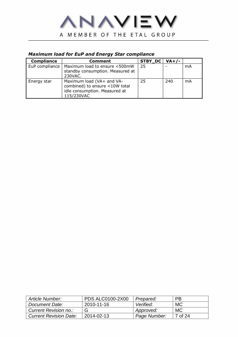
Maximum load for EuP and Energy Star compliance
Compliance Comment STBY_DC VA+/-
EuP compliance Maximum load to ensure <500mWstandby consumption. Measured at230VAC.
25 - mA
Energy star Maximum load (VA+ and VA-combined) to ensure <10W totalidle consumption. Measured at115/230VAC
25 240 mA
Article Number: PDS ALC0100-2X00 Prepared: PBDocument Date: 2010-11-16 Verified: MCCurrent Revision no.: G Approved: MCCurrent Revision Date: 2014-02-13 Page Number: 8 of 24
Protections and functions:
Mains input fuse T1.25AL (time lag)
Over temperatureprotection
Power shut down by over temperature.Threshold temperature : 90(min) - 95(typ) - 100(max)'CSensor connected to drain tab of high side power FET.
The shutdown time is short, only parts of seconds to start with, butincreases as the module heats up. This is because when thetemperature difference between the MOSFETs and the PCB islarge, the MOSFETs will cool down very fast after shutdown, but asthe PCB gets warmer it will take longer. This protection mode willbe heard as very short interrupts to the sound.
Over voltage protection Amplifier shut down during over voltage on output voltage rails.This can happen if the mains voltage exceeds the maximum ratedlevel or during railpumping (due to DC on inputs or whengenerating subsonic frequencies). Immediately when the voltagehas decreased the amplifier will start again. This protection modewill be heard as very short interrupts to the sound.
Over current protection Treshold current : 8A (0.5Ω load, 1kHz burst). There are two modes of over current protection.
1. Constant current mode. The output will behave as duringvoltage clipping i.e. the output voltage will be cut off on thetop to maintain an allowed current.
2. If the over current mode persists during a longer period(several periods of music) it is assumed that there is an errorand the amplifier will shut down for a while and then restart.
Protection output status Status output: CON2 pin 6 "STATUS"
Goes high during:3. Over temperature shutdown4. Over voltage shutdownNote that over current protection will not generate a STATUS flag.
Remote shut down tostandby mode
Shut down input: CON2 pin 5 "DISABLE"
Shut down by: Apply +8VDC (+2<V<+15VDC) on DISABLE inputNormal operation : Leave pin floating or put to GND (V<+1VDC)
Remote shut down to mutemode
Mute input: CON2 pin 7 "MUTE"
Mute by: Apply +8VDC (+2<V<+15VDC) on DISABLE inputNormal operation : Leave pin floating or put to GND (V<+1VDC)
Anti rail pumping Right audio input channel is internally inverted before amplificationin order to consume power symmetrically from both power rails.This prevents rail pumping, since the bass of recordings is usuallyequally mixed into both channels. The output of the right channelis correspondingly internally inverted, such that this feature istransparent to the user. This is seen in fig. 2When using one channel only it is still possible to generate fullspan of power at 20Hz into 4Ω at nominal mains voltage. The lower frequency that is being generated the more the rails will bepumped (DC being the extreme where even a few hundredmillivolts can cause over voltage shutdown).

Article Number: PDS ALC0100-2X00 Prepared: PBDocument Date: 2010-11-16 Verified: MCCurrent Revision no.: G Approved: MCCurrent Revision Date: 2014-02-13 Page Number: 9 of 24
Audio specifications:
Proposed interfaces:
Input/output ALC circuit Proposed interface
STATUS (output)Goes high during overvoltage conditions dueto rail pumping orduring amplifier overtemp conditions.
DISABLE (input)Pull up to STBY_DC orVA+ to set the modulein standby mode(power supply andamplifiers disabled).Leave floating or pulldown to ground toenable.
Offset voltage (open inputs) 5mV typ. (40mV max)
Switching frequency (idle) 400kHz typ. (370-430kHz min-max)
Switching recidual 350mVpk typical
Recommended load 4Ω (SE mode), minimum load 2Ω8Ω (BTL mode), minimum load 4Ω
Gain (f =1kHz) 20.0dB typical
Idle noise 25uV typical (A-weighted 20Hz < f < 20kHz)
Upper BW limit (-3dB) >60kHz
Lower BW limit (-3dB) 0Hz (requires 100% identical use of both channels)
Output impedance (100Hz) 6mΩ typical
Residual noise vs freq See figure 3
Crosstalk vs freq See figure 4
THD vs PWR See figures 6-10
THD vs freq See figure 11
Freq response See figure 12
Article Number: PDS ALC0100-2X00 Prepared: PBDocument Date: 2010-11-16 Verified: MCCurrent Revision no.: G Approved: MCCurrent Revision Date: 2014-02-13 Page Number: 10 of 24
MUTE (input)Pull up to STBY_DC orVA+ to set the modulein mute mode(amplifiers disabled).Leave floating or pulldown to ground toenable.
CONNECTIONS
Mains connector CON1 : 2 pin 0.312” (7.92mm) locking header (JST B2P3-VH (LF) (SN))
Suggested mating connector : JST VHR-3N or similarSuggested crimp terminal: SVH-41T-P1.1 or similar
PinningPin1 : AC_N (Neutral)Pin2 : AC_L (Live)
Mains input rangeconnector
CON101 : 2pin 0.156” (3.96mm) locking header (JST B2P-VH (LF) (SN))Suggested mating connector : JST VHR-2N or similarSuggested crimp terminal : SVH-41T-P1.1 or similar
Short Pin1 to Pin2 for 115VAC operation, leave open for 230VAC. Can bedone with a remote switch, with possible impact on EMI. Therefore ifremote switch is used, EMC must be verified.
Signal connector CON2 : 13pin 0.100” (2.54mm) header (Molex 2227-2131)
Suggested mating connector : Molex KK series 2695-13 or similarSuggested crimp terminal: Molex 4809 or similar
Pinning: Description:
Pin 1 : STBY_DC AUX output voltage V1. (Standby voltage)Pin 2 : VA+ AUX output voltage V2.Pin 3 : GND Secondary side ground.Pin 4 : VA- AUX output voltage V3Pin 5 : DISABLE Standby input signal.Pin 6 : STATUS Status output signal.Pin 7 : MUTE Mute input signal.Pin 8 : GND Secondary side ground.Pin 9 : GND Secondary side ground.Pin 10 : IN_L+ Left audio channel positive input.Pin 11 : IN_L- Left audio channel negative input.Pin 12 : IN_R+ Right audio channel positive input.Pin 13 : IN_R- Right audio channel negative input.
Article Number: PDS ALC0100-2X00 Prepared: PBDocument Date: 2010-11-16 Verified: MCCurrent Revision no.: G Approved: MCCurrent Revision Date: 2014-02-13 Page Number: 11 of 24
Loudspeakerconnectors
CON3 : 2pin 0.156” (3.96mm) locking header (JST B2P-VH (LF) (SN))CON4 : 2pin 0.156” (3.96mm) locking header (JST B2P-VH (LF) (SN))
Suggested mating connector : JST VHR-2N or similarSuggested crimp terminal: SVH-41T-P1.1 or similar
Pinning: Description:
CON3Pin1 : OUT_L+ Left audio channel positive output.Pin2 : OUT_L- Left audio channel negative output.CON4Pin1 : OUT_R+ Right audio channel positive output.Pin2 : OUT_R- Right audio channel negative output.
Hanger connector*optional
CON3001 : 3 pin 0.156” (3.96mm) locking header (JST B3P-VH (LF)(SN))
Suggested mating connector : JST VHR-3N or similarSuggested crimp terminal: SVH-41T-P1.1 or similar
Pinning: Description:
Pin 1 : VS- AUX output voltage V5.Pin 2 : GND Secondary side ground.Pin 3 : VS+ AUX output voltage V4.

Article Number: PDS ALC0100-2X00 Prepared: PBDocument Date: 2010-11-16 Verified: MCCurrent Revision no.: G Approved: MCCurrent Revision Date: 2014-02-13 Page Number: 12 of 24
MECHANICAL OUTLINE
Size (l x w x h) 130x75x30mm, see Figure 1. Board outline, dimensions below.
Max component height/lead length on PCB bottom side: 4.0 mm30mm height measured from bottom side of PCB to highestcomponent on top side. For total height of unit add the 4mm maxcomponent height/lead length on PCB bottom side, i.e. 34mm.
Weight 140-150g depending on model
Mounting hole dia. X1, X2 (non-plated): 3.5mmX3, X4, X5 (plated): 3.5mm
IP figures, encapsulationIP XY (X=Solids, Y=Liquids)
Open frame
Coloring, design andbranding
ALC0100-2x00, black PCB
Figure 1. Board outline, dimensions and mounting holes.

Article Number: PDS ALC0100-2X00 Prepared: PBDocument Date: 2010-11-16 Verified: MCCurrent Revision no.: G Approved: MCCurrent Revision Date: 2014-02-13 Page Number: 13 of 24
Figure 2. Connection diagram.
Figure 3. Residual noise.

Article Number: PDS ALC0100-2X00 Prepared: PBDocument Date: 2010-11-16 Verified: MCCurrent Revision no.: G Approved: MCCurrent Revision Date: 2014-02-13 Page Number: 14 of 24
Figure 4. Crosstalk 1W, 10W 4Ω 230VAC.
Figure 5. FFT 1W 4Ω 230VAC.

Article Number: PDS ALC0100-2X00 Prepared: PBDocument Date: 2010-11-16 Verified: MCCurrent Revision no.: G Approved: MCCurrent Revision Date: 2014-02-13 Page Number: 15 of 24
Figure 6. THD vs power, 4Ω 230VAC, one channel driven.

Article Number: PDS ALC0100-2X00 Prepared: PBDocument Date: 2010-11-16 Verified: MCCurrent Revision no.: G Approved: MCCurrent Revision Date: 2014-02-13 Page Number: 16 of 24
Figure 7. THD vs power, 8Ω 230VAC, one channel driven.
Figure 8. THD vs power, 4Ω 230VAC, both channels driven.

Article Number: PDS ALC0100-2X00 Prepared: PBDocument Date: 2010-11-16 Verified: MCCurrent Revision no.: G Approved: MCCurrent Revision Date: 2014-02-13 Page Number: 17 of 24
Figure 9. THD vs power, BTL mode 8Ω 230VAC. 47nF added between outputs.
Figure 10. THD vs power, 4Ω 185VAC, both channels driven.

Article Number: PDS ALC0100-2X00 Prepared: PBDocument Date: 2010-11-16 Verified: MCCurrent Revision no.: G Approved: MCCurrent Revision Date: 2014-02-13 Page Number: 18 of 24
Figure 11. THD vs frequency, 4Ω 230VAC, both channels driven.

Article Number: PDS ALC0100-2X00 Prepared: PBDocument Date: 2010-11-16 Verified: MCCurrent Revision no.: G Approved: MCCurrent Revision Date: 2014-02-13 Page Number: 19 of 24
Figure 12. Frequency response.
INSTRUCTIONS
Replacing the VA+/- fuse
The auxiliary supplies VA+/- are protected by a surface mounted fuse. In case ofoverload this fuse will open and has to be replaced to get the supplies back.
F200 is a 1.25A fast acting fuse from Littelfuse with article number 04401.25.
APPLICATION NOTES
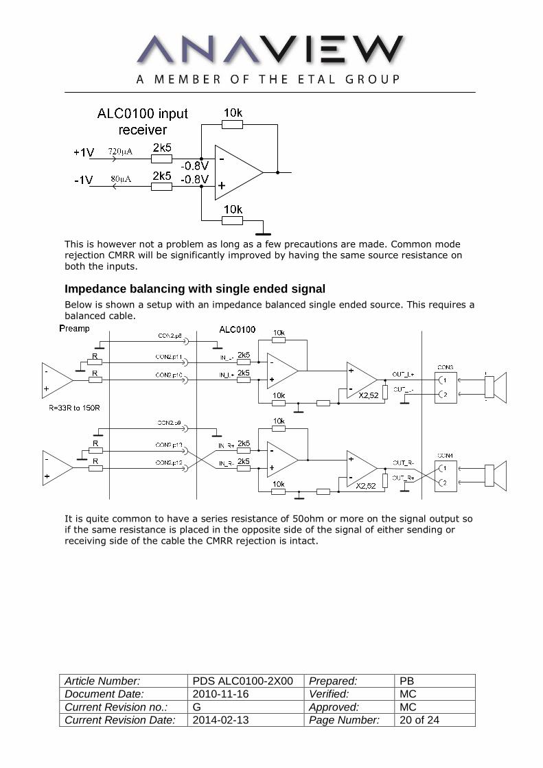
Optimizing input stage CMRR
This is simplified drawing of the input of ALC0180. It is a typical circuit which is oftenused where the source impedance is well known and does not vary too much. Inputcurrents are calculated when a balanced signal is applied. As can be seen the inputimpedance is not the same on both inputs and depending on which type of signal isapplied (single ended or balanced) the input impedance changes.
Article Number: PDS ALC0100-2X00 Prepared: PBDocument Date: 2010-11-16 Verified: MCCurrent Revision no.: G Approved: MCCurrent Revision Date: 2014-02-13 Page Number: 20 of 24
This is however not a problem as long as a few precautions are made. Common moderejection CMRR will be significantly improved by having the same source resistance onboth the inputs.
Impedance balancing with single ended signal
Below is shown a setup with an impedance balanced single ended source. This requires abalanced cable.
It is quite common to have a series resistance of 50ohm or more on the signal output soif the same resistance is placed in the opposite side of the signal of either sending orreceiving side of the cable the CMRR rejection is intact.
Article Number: PDS ALC0100-2X00 Prepared: PBDocument Date: 2010-11-16 Verified: MCCurrent Revision no.: G Approved: MCCurrent Revision Date: 2014-02-13 Page Number: 21 of 24
Balanced input signal
If a balanced signal source is used the following setup applies.
If long cables are used the cable impedance itself can contribute in a non insignificantway to the series impedance and since that impedance is not very well defined(symmetrically) it can be an advantage to increase both the diff mode and commonmode input impedance. In such a case an additional circuit as below can be added beforethe AMS module.
Article Number: PDS ALC0100-2X00 Prepared: PBDocument Date: 2010-11-16 Verified: MCCurrent Revision no.: G Approved: MCCurrent Revision Date: 2014-02-13 Page Number: 22 of 24
BTL setup
SE input signal
Balanced input signal

Article Number: PDS ALC0100-2X00 Prepared: PBDocument Date: 2010-11-16 Verified: MCCurrent Revision no.: G Approved: MCCurrent Revision Date: 2014-02-13 Page Number: 23 of 24
REVISIONS LOG
Rev. Date Item Sign
A 2010-11-16 - First revision MC
B 2010-12-07
- Output current reduced to 8A- Fuse changed to T1.25AL- Outline picture updated- Changed Max sourcing current needed to MUTE
MC
C 2011-06-01
- Changed min DISABLE and MUTE activation voltage to 2VDC- Updated all figures- Updated almost all numbers- Added information about different variants- Important: this technical spec is still in draft form; information &specifications are subject to change.
MC
D 2011-12-02
- Updated connection figure to also show BTL connection and inputresistor values- Added crimp terminal information to mating connectors- Added further description of MUTE and DISABLE function- Added figure with output power at 185VAC mains input voltage- Added customer approval box- Updated AP plots
MC
E 2013-05-17 - Updated to Anaview standards MD
F 2013-10-15- Further updated to Anaview standards- Name change to PDS ALC0100-2X00- Updated Safety Standards
JNPB
G 2014-02-13
- Added application notes on input stage- Added information about VA+/- fuse- Added proposed interfaces for inputs/outputs- Added information in protection and audio specifications sections.- Changed PCB color to black.- Updated specs for VA+/-- Added specs for Energy Star compliance- Recalculated input impedance in INPUT SPECIFICATIONS- Updated EMC info
PBJN
Article Number: PDS ALC0100-2X00 Prepared: PBDocument Date: 2010-11-16 Verified: MCCurrent Revision no.: G Approved: MCCurrent Revision Date: 2014-02-13 Page Number: 24 of 24
ANAVIEW CONTACT INFORMATION
For further information about Anaview’s products and technology please contact:Email: [email protected]: www.anaview.com
Anaview (Europe, APAC)
Södergatan 425225 HelsingborgSweden
Anaview (North America)
PO Box 459Manasquan, NJ 08736New JerseyUSA
Part ofETAL Group ABFagerstagatan 3SE-163 53 SPÅNGASWEDEN


