
HUAWEI TECHNOLOGIES CO., LTD.
www.huawei.com
PDN design and analysis methodology in SI&PI co-design
Asian IBIS Summit, November 9, 2010, Shenzhen China
Luo Zipeng ([email protected])
Liu Shuyao ([email protected])

HUAWEI TECHNOLOGIES CO., LTD. Page 2
Agenda
SI&PI co-design challengeKey parameters in PDN designModeling the loop inductance of high frequency capacitorHigh frequency capacitor' global decouple effectTight coupling Power-Gnd pair in board’ PDNSSN analysis of PDN’ SI&PI co-design via PDN’ IBIS model
HUAWEI TECHNOLOGIES CO., LTD.
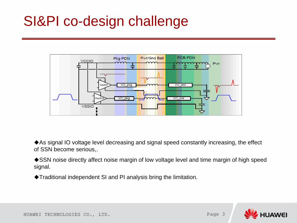
SI&PI co-design challenge
Page 3
As signal IO voltage level decreasing and signal speed constantly increasing, the effect of SSN become serious,.
SSN noise directly affect noise margin of low voltage level and time margin of high speed signal.
Traditional independent SI and PI analysis bring the limitation.

HUAWEI TECHNOLOGIES CO., LTD. Page 4
Key parameters in PDN design
Board’ PDN sketch map
Equivalent circuit of board’ PDN
PDN of Board:VRM
Bulk capacitor
High frequency capacitor
Power-Gnd plane capacitor
Chip’ PDN
High frequency capacitor and Power-Gnd plane play an important role in PDN design;
HUAWEI TECHNOLOGIES CO., LTD. Page 5
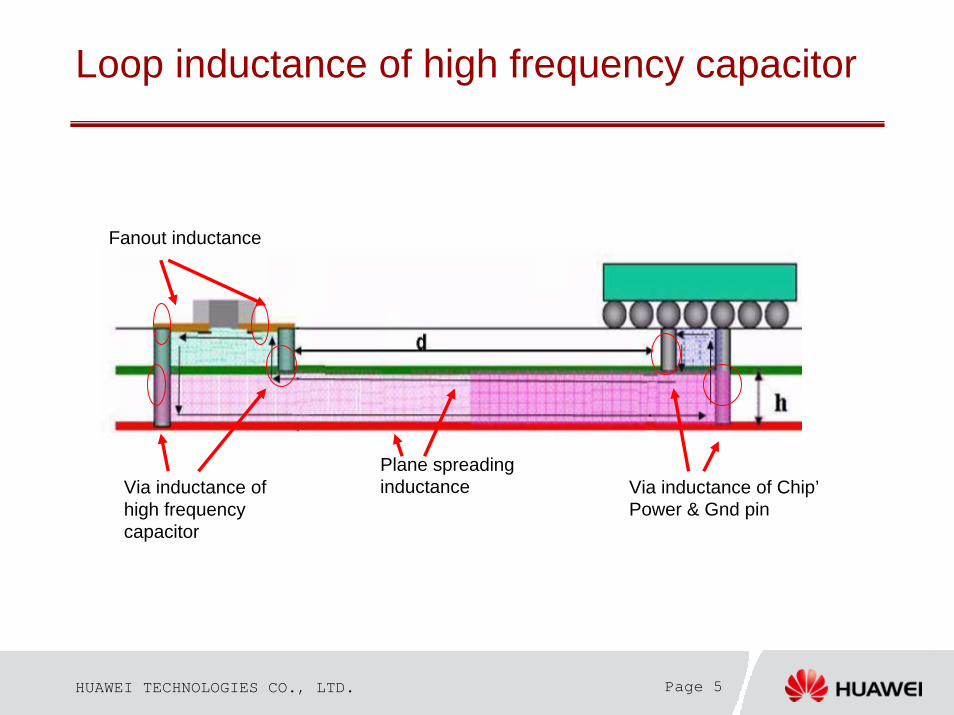
Loop inductance of high frequency capacitor
Fanout inductance
Via inductance of high frequency capacitor
Plane spreading inductance Via inductance of Chip’
Power & Gnd pin

HUAWEI TECHNOLOGIES CO., LTD. Page 6
Via inductance effect in Loop inductance
Capacitor’ ESL: 0.4~0.65nH;
Special fanout inductance: 0.25~0.3nH;
Plane spreading inductance: hundreds of pH;
Via inductance of Capacitor: 1nH~2.5nH,when in different stackup, The Value will be varied

HUAWEI TECHNOLOGIES CO., LTD. Page 7
Modeling the via inductance
Via inductance is about 75%~80% of the total loop inductance;
As the the Power-Gnd pair space and location changed, the via inductance of capacitor may varies;
Optimizing the design of Power-Gnd pair will decrease the via inductance, increase the decouple effect of high frequency capacitor;
Evaluate the value of via inductance by simulation, comparison between simulation and measurement validate the precision of via inductance model.
measurement Simulation precision
2.29nH 2.25nH 98%
HUAWEI TECHNOLOGIES CO., LTD. Page 8
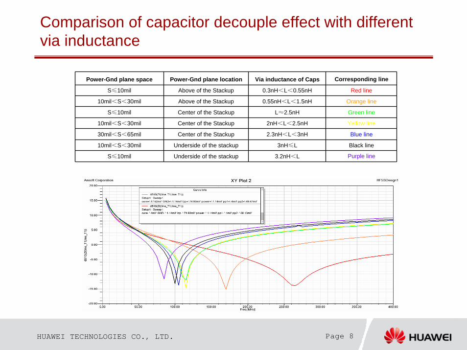
Comparison of capacitor decouple effect with different via inductance
Power-Gnd plane space Power-Gnd plane location Via inductance of Caps Corresponding line
S≤10mil Above of the Stackup 0.3nH<L<0.55nH Red line
10mil<S<30mil Above of the Stackup 0.55nH<L<1.5nH Orange line
S≤10mil Center of the Stackup L≈2.5nH Green line
10mil<S<30mil Center of the Stackup 2nH<L<2.5nH Yellow line
30mil<S<65mil Center of the Stackup 2.3nH<L<3nH Blue line
10mil<S<30mil Underside of the stackup 3nH≤L Black line
S≤10mil Underside of the stackup 3.2nH<L Purple line

HUAWEI TECHNOLOGIES CO., LTD. Page 9
Plane spreading inductance affect high frequency cap decouple
Fanout inductance of cap
Via inductance of C
ap
Plane spreading inductance
Designing the PDN of PCB, in order to decrease loop inductance of capacitor, high frequency decoupling capacitor will be located as close as possible to chips‘ power pin;
High frequency decaps usually locate under the chip, close to the power pin;
In actual design, Both chips and decapsneed to be located on top side of PCB, for the limitation of chip's dimension, decapsonly can be near to the chips, not close to power pin,
as seen as left fig B, plane spreading inductance increase while both chip and decap be located on top side of PCB;
Compared with fig A, the total loop inductance in fig B will increase, and High frequency capacitor’ decouple effect obviously decrease;
A
B

HUAWEI TECHNOLOGIES CO., LTD. Page 10
Global decouple effect of high frequency cap
As decreasing the space between the Power Ground plane, the total loop inductance also decrease, and high frequency caps will show an global decouple effect.
HUAWEI TECHNOLOGIES CO., LTD. Page 11
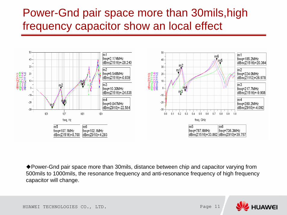
Power-Gnd pair space more than 30mils,high frequency capacitor show an local effect
Power-Gnd pair space more than 30mils, distance between chip and capacitor varying from 500mils to 1000mils, the resonance frequency and anti-resonance frequency of high frequency capacitor will change.

HUAWEI TECHNOLOGIES CO., LTD. Page 12
Power-Gnd pair space less than 10mils,high frequency capacitor show an global effect
Power-Gnd pair space less than 10mils, distance between chip and capacitor varying from 500mils to 1000mils, the resonance frequency and anti-resonance frequency of high frequency capacitor almost keep same.

HUAWEI TECHNOLOGIES CO., LTD. Page 13
Power-Gnd pair space effect analysis of PDN design
Distance between chip and capacitor keep constant, power-gnd pair space varying from 5.12mils to 56.2mils, the resonance frequency and anti-resonance frequency of high frequency capacitor change.

HUAWEI TECHNOLOGIES CO., LTD. Page 14
Tight coupling Power-Gnd pair in PDN
Power-gnd space 5.12mils,power-gnd pair tightly couple
Power-gnd space 17.52mils
HUAWEI TECHNOLOGIES CO., LTD. Page 15Page 15
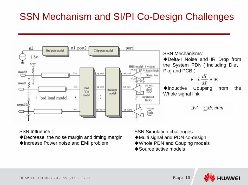
SSN Mechanism and SI/PI Co-Design Challenges
SSN Mechanisms: Delta-I Noise and IR Drop from
the System PDN(Including Die、Pkg and PCB)
Inductive Coupling from the Whole signal link
SSN Influence :Decrease the noise margin and timing marginIncrease Power noise and EMI problem
SSN Simulation challenges :Multi signal and PDN co-designWhole PDN and Couping modelsSource active models
HUAWEI TECHNOLOGIES CO., LTD. Page 16Page 16
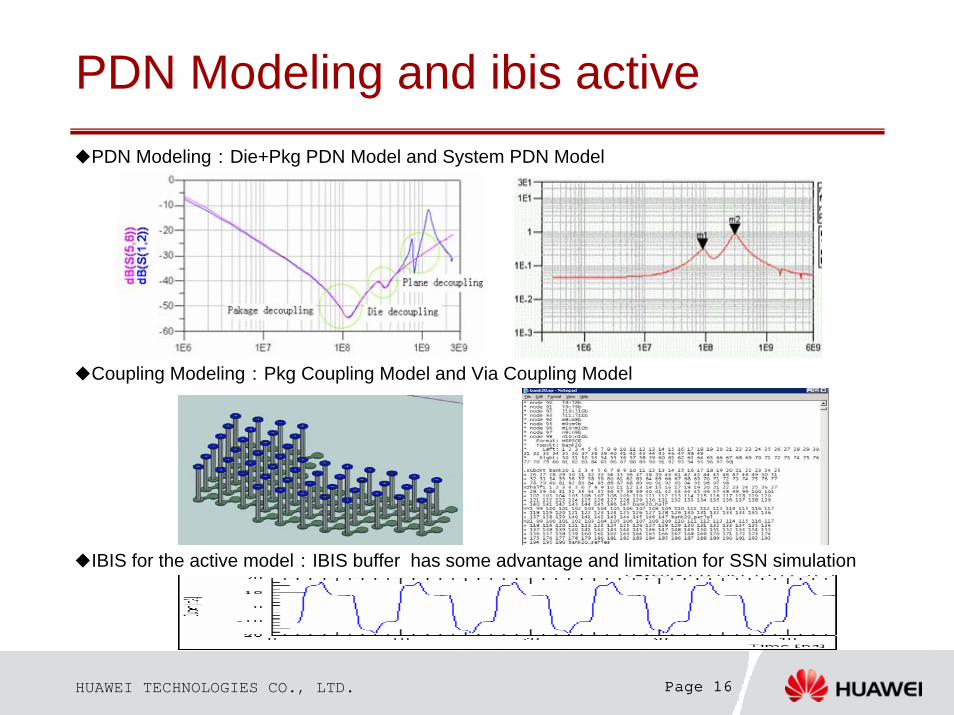
PDN Modeling and ibis active PDN Modeling:Die+Pkg PDN Model and System PDN Model
IBIS for the active model:IBIS buffer has some advantage and limitation for SSN simulation
Coupling Modeling:Pkg Coupling Model and Via Coupling Model
HUAWEI TECHNOLOGIES CO., LTD. Page 17Page 17
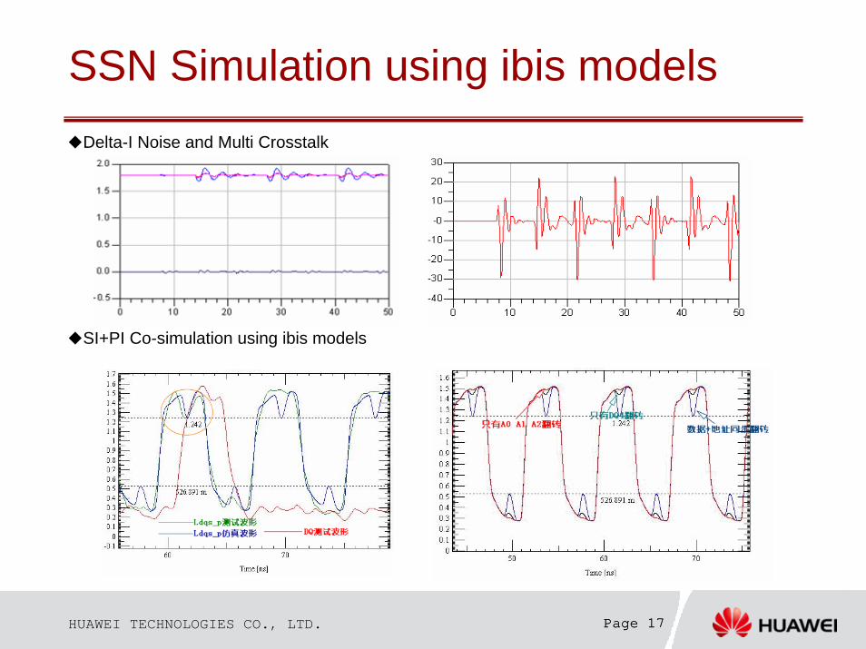
SSN Simulation using ibis models Delta-I Noise and Multi Crosstalk
SI+PI Co-simulation using ibis models

HUAWEI TECHNOLOGIES CO., LTD. Page 18Page 18
Conclusion
PDN directly determine the board’ power delivery system design quality, and in board’ PDN high frequency capacitor and Power-Gnd plane play an important role;
The loop inductance of high frequency capacitor decrease as smaller as possible in a well designed PDN ,and capacitor show an global decouple effect;
The tight coupling PDN adequately consider power-gnd plane capacitor, expanding the efficiency frequency band;SSN analysis via PDN’ IBIS model enhance simulation efficiency and speed. Implementing
SI&PI co-design.

Thank youwww.huawei.com


