
ESMT F25L01PA (2D)
Elite Semiconductor Memory Technology Inc. Publication Date: Apr. 2013 Revision: 1.2 1/31
Flash 3V Only 1 M bit Serial Flash Memory with Dual Output
FEATURES Single supply voltage 2.7~3.6V Standard, Dual SPI
Speed - Read max frequency: 33MHz - Fast Read max frequency: 50MHz; 86MHz; 100MHz - Fast Read Dual max frequency: 50MHz / 86MHz (100MHz / 172MHz equivalent Dual SPI)
Low power consumption - Active current: 22 mA - Standby current: 25μA - Deep Power Down current: 10μA
Reliability - 100,000 typical program/erase cycles - 20 years Data Retention
Program - Page programming time: 1.5 ms (typical)
Erase - Chip erase time 1 sec (typical) - Block erase time 0.75 sec (typical) - Sector erase time 90 ms (typical)
Page Programming - 256 byte per programmable page
SPI Serial Interface - SPI Compatible: Mode 0 and Mode 3
End of program or erase detection
Write Protect ( WP )
Hold Pin ( HOLD )
All Pb-free products are RoHS-Compliant
ORDERING INFORMATION
Product ID Speed Package Comments
F25L01PA –50PG2D 50MHz
F25L01PA –86PG2D 86MHz
F25L01PA –100PG2D 100MHz
8-lead SOIC 150 mil Pb-free
F25L01PA –50SG2D 50MHz
F25L01PA –86SG2D 86MHz
F25L01PA –100SG2D 100MHz
8-pin TSSOP
173 mil (4.4mm) Pb-free
GENERAL DESCRIPTION
The F25L01PA is a 1Megabit, 3V only CMOS Serial Flash memory device. The device supports the standard Serial Peripheral Interface (SPI), and a Dual SPI. ESMT’s memory devices reliably store memory data even after 100,000 programming and erase cycles. The memory array can be organized into 512 programmable pages of 256 byte each. 1 to 256 byte can be programmed at a time with the Page Program instruction. The device features sector erase architecture. The memory array
is divided into 32 uniform sectors with 4K byte each; 2 uniform blocks with 64K byte each. Sectors can be erased individually without affecting the data in other sectors. Blocks can be erased individually without affecting the data in other blocks. Whole chip erase capabilities provide the flexibility to revise the data in the device. The device has Sector, Block or Chip Erase but no page erase. The sector protect/unprotect feature disables both program and erase operations in any combination of the sectors of the memory.
ESMT F25L01PA (2D)
Elite Semiconductor Memory Technology Inc. Publication Date: Apr. 2013 Revision: 1.2 2/31
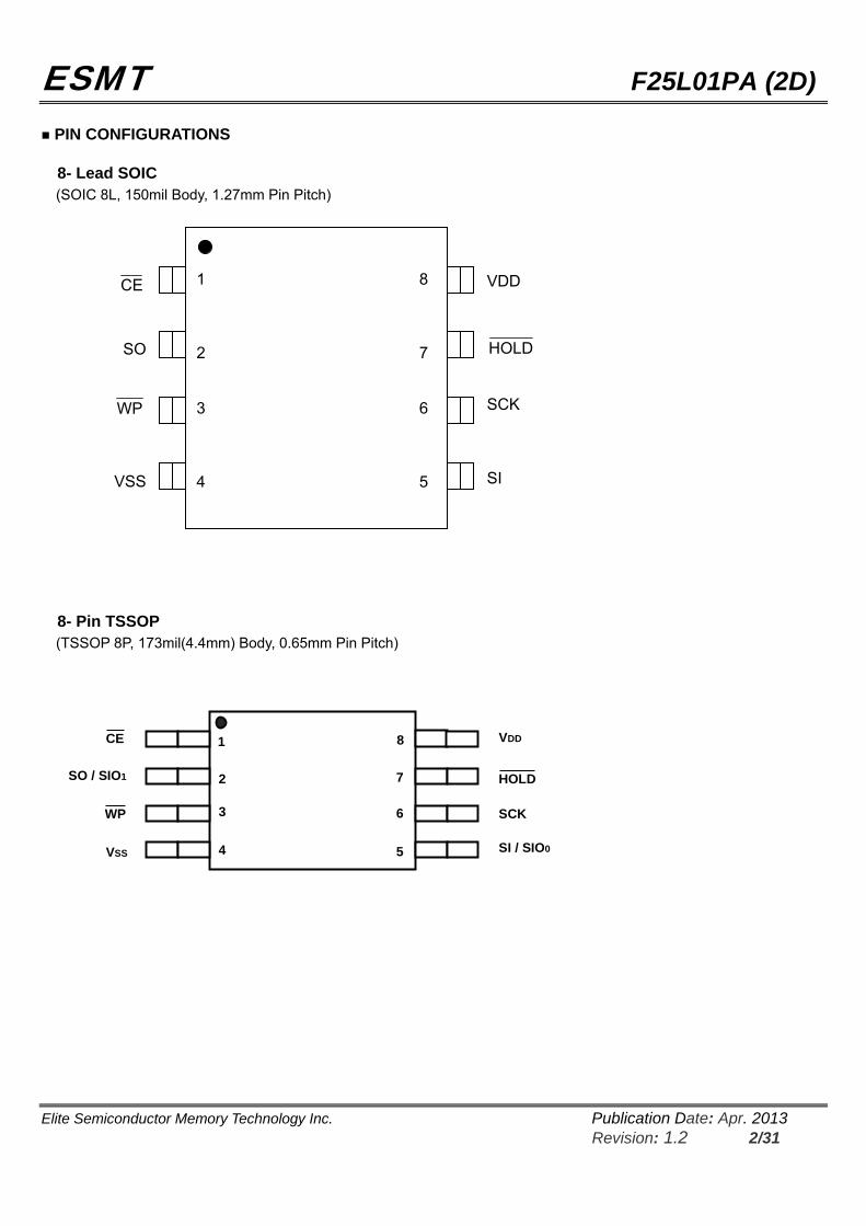
PIN CONFIGURATIONS
8- Lead SOIC (SOIC 8L, 150mil Body, 1.27mm Pin Pitch)
8- Pin TSSOP (TSSOP 8P, 173mil(4.4mm) Body, 0.65mm Pin Pitch)
1
2
3
4
8
7
6
5
CE
SO / SIO1
WP
VSS
VDD
HOLD
SCK
SI / SIO0
1 8 2 7 3 6 4 5
VDD
HOLD SCK SI
CE
SO
WP
VSS

ESMT F25L01PA (2D)
Elite Semiconductor Memory Technology Inc. Publication Date: Apr. 2013 Revision: 1.2 3/31
PIN DESCRIPTION
Symbol Pin Name Functions
SCK Serial Clock To provide the timing for serial input and output operations
SI Serial Data Input To transfer commands, addresses or data serially into the device. Data is latched on the rising edge of SCK.
SO Serial Data Output To transfer data serially out of the device. Data is shifted out on the falling edge of SCK.
CE Chip Enable To activate the device when CE is low.
WP Write Protect The Write Protect ( WP ) pin is used to enable/disable BPL bit in the status register.
HOLD Hold To temporality stop serial communication with SPI flash memory without resetting the device.
VDD Power Supply To provide power. VSS Ground

ESMT F25L01PA (2D)
Elite Semiconductor Memory Technology Inc. Publication Date: Apr. 2013 Revision: 1.2 4/31
FUNCTIONAL BLOCK DIAGRAM
AddressBuffers
andLatches
X-Decoder Flash
Y-Decoder
I/O Buttersand
Data Latches
Serial Interface
Control Logic
CE SCK SI WPSO HOLD
SECTOR STRUCTURE
Table 1: F25L01PA Sector Address Table
Block Address Block Sector Sector Size
(Kbytes) Address range A16
31 4KB 01F000H – 01FFFFH : : : 1
16 4KB 010000H – 010FFFH 1
15 4KB 00F000H – 00FFFFH : : : 0 0 4KB 000000H – 000FFFH
0
ESMT F25L01PA (2D)
Elite Semiconductor Memory Technology Inc. Publication Date: Apr. 2013 Revision: 1.2 5/31
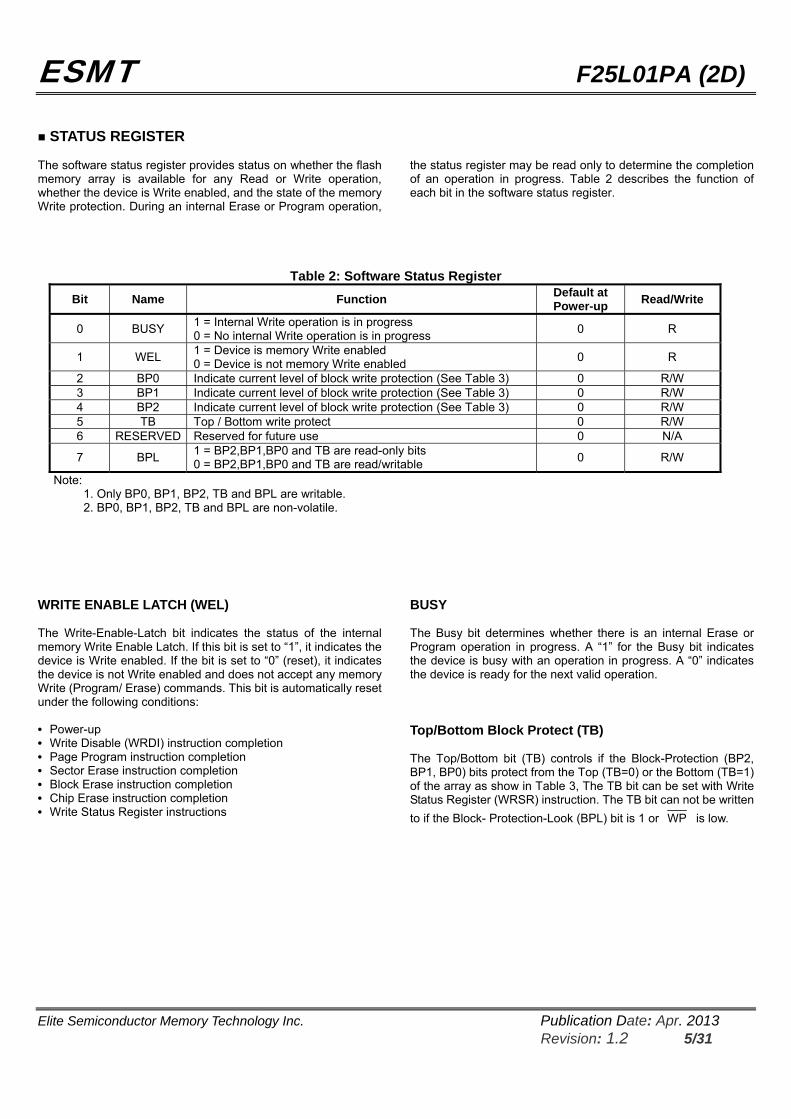
STATUS REGISTER The software status register provides status on whether the flash memory array is available for any Read or Write operation, whether the device is Write enabled, and the state of the memory Write protection. During an internal Erase or Program operation,
the status register may be read only to determine the completion of an operation in progress. Table 2 describes the function of each bit in the software status register.
Table 2: Software Status Register Bit Name Function Default at
Power-up Read/Write
0 BUSY 1 = Internal Write operation is in progress 0 = No internal Write operation is in progress 0 R
1 WEL 1 = Device is memory Write enabled 0 = Device is not memory Write enabled 0 R
2 BP0 Indicate current level of block write protection (See Table 3) 0 R/W 3 BP1 Indicate current level of block write protection (See Table 3) 0 R/W 4 BP2 Indicate current level of block write protection (See Table 3) 0 R/W 5 TB Top / Bottom write protect 0 R/W 6 RESERVED Reserved for future use 0 N/A
7 BPL 1 = BP2,BP1,BP0 and TB are read-only bits 0 = BP2,BP1,BP0 and TB are read/writable 0 R/W
Note: 1. Only BP0, BP1, BP2, TB and BPL are writable. 2. BP0, BP1, BP2, TB and BPL are non-volatile.
WRITE ENABLE LATCH (WEL) The Write-Enable-Latch bit indicates the status of the internal memory Write Enable Latch. If this bit is set to “1”, it indicates the device is Write enabled. If the bit is set to “0” (reset), it indicates the device is not Write enabled and does not accept any memory Write (Program/ Erase) commands. This bit is automatically reset under the following conditions: • Power-up • Write Disable (WRDI) instruction completion • Page Program instruction completion • Sector Erase instruction completion • Block Erase instruction completion • Chip Erase instruction completion • Write Status Register instructions
BUSY The Busy bit determines whether there is an internal Erase or Program operation in progress. A “1” for the Busy bit indicates the device is busy with an operation in progress. A “0” indicates the device is ready for the next valid operation. Top/Bottom Block Protect (TB) The Top/Bottom bit (TB) controls if the Block-Protection (BP2, BP1, BP0) bits protect from the Top (TB=0) or the Bottom (TB=1) of the array as show in Table 3, The TB bit can be set with Write Status Register (WRSR) instruction. The TB bit can not be written to if the Block- Protection-Look (BPL) bit is 1 or WP is low.

ESMT F25L01PA (2D)
Elite Semiconductor Memory Technology Inc. Publication Date: Apr. 2013 Revision: 1.2 6/31
Table 3: F25L01PA Block Protection Table
Status Register Bit Protected Memory Area Protection Level
TB BP2 BP1 BP0 Block Range Address Range 0 X 0 0 0 None None 0* X 1 0 0 None None
Upper 1/2 0 X 0 1 Block 1 010000H – 01FFFFH Lower 1/2 1 X 0 1 Block 0 000000H – 00FFFFH All Blocks X X 1 X Block 0~1 000000H –00FFFFH
Note: * The combination of Status Register Bit (X100) can’t use Chip Erase instruction. Block Protection (BP2, BP1, BP0) The Block-Protection (BP2, BP1, BP0) bits define the size of the memory area, as defined in Table 3, to be software protected against any memory Write (Program or Erase) operations. The Write Status Register (WRSR) instruction is used to program the BP2, BP1, BP0 bits as long as WP is high or the Block- Protection-Look (BPL) bit is 0. Chip Erase can only be executed if Block-Protection bits are all 0. The factory default setting for Block Protection Bit (BP2 ~ BP0) is 0.
Block Protection Lock-Down (BPL) WP pin driven low (VIL), enables the Block-Protection- Lock-Down (BPL) bit. When BPL is set to 1, it prevents any further alteration of the TB, BPL, BP2, BP1, and BP0 bits. When the WP pin is driven high (VIH), the BPL bit has no effect and its value is “Don’t Care”.
ESMT F25L01PA (2D)
Elite Semiconductor Memory Technology Inc. Publication Date: Apr. 2013 Revision: 1.2 7/31
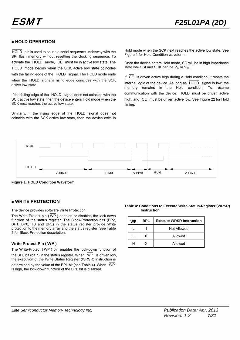
HOLD OPERATION HOLD pin is used to pause a serial sequence underway with the SPI flash memory without resetting the clocking sequence. To activate the HOLD mode, CE must be in active low state. The
HOLD mode begins when the SCK active low state coincides
with the falling edge of the HOLD signal. The HOLD mode ends
when the HOLD signal’s rising edge coincides with the SCK active low state. If the falling edge of the HOLD signal does not coincide with the SCK active low state, then the device enters Hold mode when the SCK next reaches the active low state. Similarly, if the rising edge of the HOLD signal does not coincide with the SCK active low state, then the device exits in
Hold mode when the SCK next reaches the active low state. See Figure 1 for Hold Condition waveform. Once the device enters Hold mode, SO will be in high impedance state while SI and SCK can be VIL or VIH. If CE is driven active high during a Hold condition, it resets the
internal logic of the device. As long as HOLD signal is low, the memory remains in the Hold condition. To resume communication with the device, HOLD must be driven active
high, and CE must be driven active low. See Figure 22 for Hold timing.
A c t ive H o ld A c ti ve H old A c t ive
H O L D
S C K
Figure 1: HOLD Condition Waveform
WRITE PROTECTION The device provides software Write Protection. The Write-Protect pin ( WP ) enables or disables the lock-down function of the status register. The Block-Protection bits (BP2, BP1, BP0, TB and BPL) in the status register provide Write protection to the memory array and the status register. See Table 3 for Block-Protection description. Write Protect Pin ( WP ) The Write-Protect ( WP ) pin enables the lock-down function of the BPL bit (bit 7) in the status register. When WP is driven low, the execution of the Write Status Register (WRSR) instruction is determined by the value of the BPL bit (see Table 4). When WP is high, the lock-down function of the BPL bit is disabled.
Table 4: Conditions to Execute Write-Status-Register (WRSR) Instruction
WP BPL Execute WRSR Instruction
L 1 Not Allowed
L 0 Allowed
H X Allowed

ESMT F25L01PA (2D)
Elite Semiconductor Memory Technology Inc. Publication Date: Apr. 2013 Revision: 1.2 8/31
INSTRUCTIONS Instructions are used to Read, Write (Erase and Program), and configure the F25L01PA. The instruction bus cycles are 8 bits each for commands (Op Code), data, and addresses. Prior to executing any Page Program, Write Status Register, Sector Erase, Block Erase, or Chip Erase instructions, the Write Enable (WREN) instruction must be executed first. The complete list of the instructions is provided in Table 5. All instructions are synchronized off a high to low transition of CE . Inputs will be accepted on the rising edge of SCK starting with the most significant bit. CE must be driven low before an instruction is
entered and must be driven high after the last bit of the instruction has been shifted in (except for Read, Read ID, Read Status Register, Read Electronic Signature instructions). Any low to high transition on CE , before receiving the last bit of an instruction bus cycle, will terminate the instruction in progress and return the device to the standby mode. Instruction commands (Op Code), addresses, and data are all input from the most significant bit (MSB) first.
Table 5: Device Operation Instructions
Bus Cycle 1~3
1 2 3 4 5 6 N Operation Max. Freq
SIN SOUT SIN SOUT SIN SOUT SIN SOUT SIN SOUT SIN SOUT SIN SOUT
Read 33 MHz 03H Hi-Z A23-A16 Hi-Z A15-A8 Hi-Z A7-A0 Hi-Z X DOUT0 X DOUT1 X cont.
Fast Read13 50 MHz
~ 100 MHz
0BH Hi-Z A23-A16 Hi-Z A15-A8 Hi-Z A7-A0 Hi-Z X X X DOUT0 X cont.
Fast Read Dual Output11,12
50 MHz ~
86 MHz 3BH A23-A16 A15-A8 A7-A0 X DOUT0~1 cont.
Sector Erase4 (4K Byte) 20H Hi-Z A23-A16 Hi-Z A15-A8 Hi-Z A7-A0 Hi-Z - - - - - - Block Erase4, (64K Byte) D8H Hi-Z A23-A16 Hi-Z A15-A8 Hi-Z A7-A0 Hi-Z - - - - - -
Chip Erase 60H / C7H Hi-Z - - - - - - - - - - - -
Page Program (PP) 02H Hi-Z A23-A16 Hi-Z A15-A8 Hi-Z A7-A0 Hi-Z DIN0 Hi-Z DIN1 Hi-Z Up to 256
bytes Hi-Z
Read Status Register (RDSR) 6 05H Hi-Z X DOUT - - - - - - - - - -
Write Status Register (WRSR) 01H Hi-Z DIN Hi-Z - - -. - - - - - - -
Write Enable (WREN) 9 06H Hi-Z - - - - - - - - - - - - Write Disable (WRDI) 04H Hi-Z - - - - - - - - - - - - Deep Power Down (DP) B9h Hi-Z - - - - - - - - - - - - Release from Deep Power Down (RDP) ABH Hi-Z - - - - - - - - - - - -
Read Electronic Signature (RES) 7 ABH Hi-Z X X X X X X X 10H - - - -
Jedec Read ID (JEDEC-ID) 8 9FH Hi-Z X 8CH X 30H X 11H - - - - - -
00H Hi-Z X 8CH X 10H - - Read ID (RDID) 10
50 MHz
~
100 MHz
90H Hi-Z 00H Hi-Z 00H Hi-Z 01H Hi-Z X 10H X 8CH - - Note:
1. Operation: SIN = Serial In, SOUT = Serial Out, Bus Cycle 1 = Op Code 2. X = Dummy Input Cycles (VIL or VIH); - = Non-Applicable Cycles (Cycles are not necessary); cont. = continuous 3. One bus cycle is eight clock periods. 4. Sector Earse addresses: use AMS -A12, remaining addresses can be VIL or VIH Block Earse addresses: use AMS -A16, remaining addresses can be VIL or VIH 5. To continue programming to the next sequential address location, enter the 8-bit command, followed by the data to be
programmed. 6. The Read-Status-Register is continuous with ongoing clock cycles until terminated by a low to high transition on CE .
7. The Read-Electronic-Signature is continuous with on going clock cycles until terminated by a low to high transition on CE . 8. The Jedec-Read-ID is output first byte 8CH as manufacture ID; second byte 30H as memory type; third byte 11H as
memory capacity.
ESMT F25L01PA (2D)
Elite Semiconductor Memory Technology Inc. Publication Date: Apr. 2013 Revision: 1.2 9/31
9. The Write-Enable (WREN) instruction and the Write-Status-Register (WRSR) instruction must work in conjunction of each other. The WRSR instruction must be executed immediately (very next bus cycle) after the WREN instruction to make both instructions effective. WREN can enable WRSR, user just need to execute it. A successful WRSR can reset WREN.
10. The Manufacture ID and Device ID output will repeat continuously until CE terminates the instruction. 11. Dual commands use bidirectional IO pins. DOUT and cont. are serial data out; others are serial data in. 12. Dual output data:
IO0 = (D6, D4, D2, D0), (D6, D4, D2, D0)IO1 = (D7, D5, D3, D1), (D7, D5, D3, D1)
DOUT0 DOUT1 13. Max. load capacitance is 15 pF.
ESMT F25L01PA (2D)
Elite Semiconductor Memory Technology Inc. Publication Date: Apr. 2013 Revision: 1.2 10/31
CE
SCK
SI
0 1 2 3 4 5 6 7 8 15 16 23 24 31 32 39 40 47 48 55 56 63 64 80
N+4
DOUT
N+3
DOUT
N+2
DOUT
N+1
DOUT
N
DOUT
MSB
MSBMSB
HIGH IMPENANCESO
0B ADD. ADD. ADD.
MODE3MODE0
71 72
X
Note : X = Dummy Byte : 8 Clocks Input Dummy (VIL or VIH)
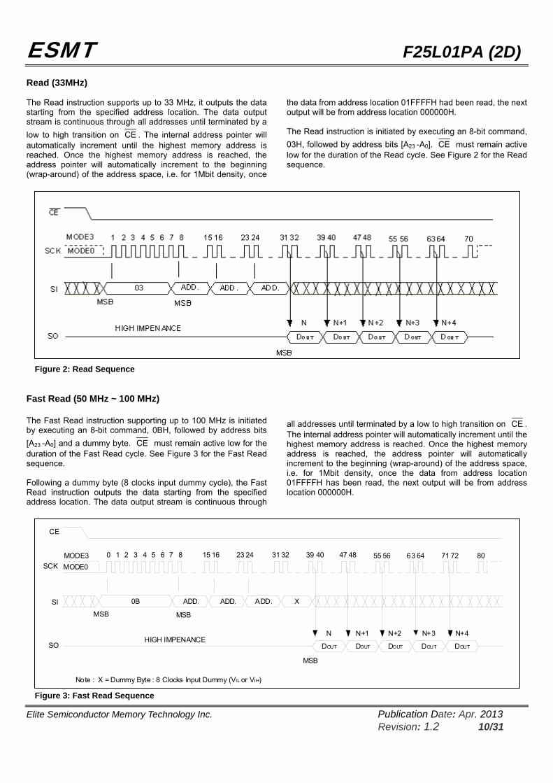
Read (33MHz) The Read instruction supports up to 33 MHz, it outputs the data starting from the specified address location. The data output stream is continuous through all addresses until terminated by a low to high transition on CE . The internal address pointer will automatically increment until the highest memory address is reached. Once the highest memory address is reached, the address pointer will automatically increment to the beginning (wrap-around) of the address space, i.e. for 1Mbit density, once
the data from address location 01FFFFH had been read, the next output will be from address location 000000H. The Read instruction is initiated by executing an 8-bit command, 03H, followed by address bits [A23 -A0]. CE must remain active low for the duration of the Read cycle. See Figure 2 for the Read sequence.
Figure 2: Read Sequence
Fast Read (50 MHz ~ 100 MHz) The Fast Read instruction supporting up to 100 MHz is initiated by executing an 8-bit command, 0BH, followed by address bits [A23 -A0] and a dummy byte. CE must remain active low for the duration of the Fast Read cycle. See Figure 3 for the Fast Read sequence. Following a dummy byte (8 clocks input dummy cycle), the Fast Read instruction outputs the data starting from the specified address location. The data output stream is continuous through
all addresses until terminated by a low to high transition on CE . The internal address pointer will automatically increment until the highest memory address is reached. Once the highest memory address is reached, the address pointer will automatically increment to the beginning (wrap-around) of the address space, i.e. for 1Mbit density, once the data from address location 01FFFFH has been read, the next output will be from address location 000000H.
Figure 3: Fast Read Sequence

ESMT F25L01PA (2D)
Elite Semiconductor Memory Technology Inc. Publication Date: Apr. 2013 Revision: 1.2 11/31
Fast Read Dual Output (50 MHz ~ 86 MHz) The Fast Read Dual Output (3BH) instruction is similar to the standard Fast Read (0BH) instruction except the data is output on SI and SO pins. This allows data to be transferred from the device at twice the rate of standard SPI devices. This instruction is for quickly downloading code from Flash to RAM upon power-up or for applications that cache code- segments to RAM for execution.
The Fast Read Dual Output instruction is initiated by executing an 8-bit command, 3BH, followed by address bits [A23 -A0] and a dummy byte. CE must remain active low for the duration of the Fast Read Dual Output cycle. See Figure 4 for the Fast Read Dual Output sequence.
Figure 4: Fast Read Dual Output Sequence
ESMT F25L01PA (2D)
Elite Semiconductor Memory Technology Inc. Publication Date: Apr. 2013 Revision: 1.2 12/31
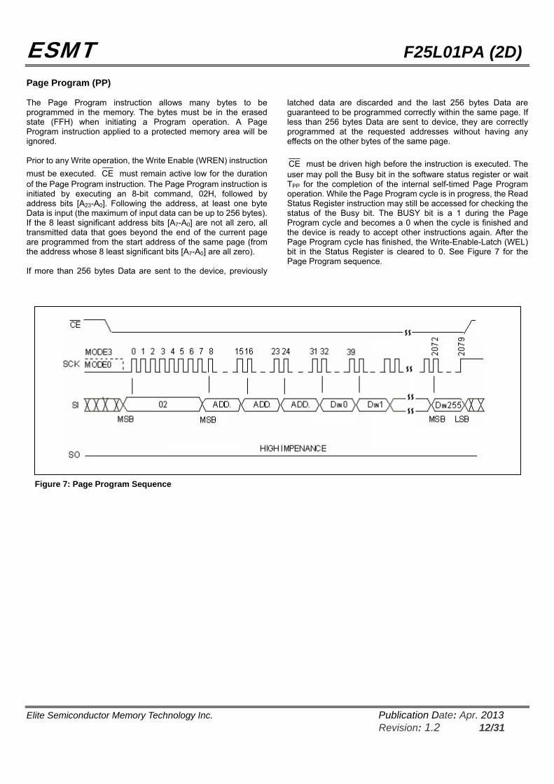
Page Program (PP) The Page Program instruction allows many bytes to be programmed in the memory. The bytes must be in the erased state (FFH) when initiating a Program operation. A Page Program instruction applied to a protected memory area will be ignored. Prior to any Write operation, the Write Enable (WREN) instruction must be executed. CE must remain active low for the duration of the Page Program instruction. The Page Program instruction is initiated by executing an 8-bit command, 02H, followed by address bits [A23-A0]. Following the address, at least one byte Data is input (the maximum of input data can be up to 256 bytes). If the 8 least significant address bits [A7-A0] are not all zero, all transmitted data that goes beyond the end of the current page are programmed from the start address of the same page (from the address whose 8 least significant bits [A7-A0] are all zero). If more than 256 bytes Data are sent to the device, previously
latched data are discarded and the last 256 bytes Data are guaranteed to be programmed correctly within the same page. If less than 256 bytes Data are sent to device, they are correctly programmed at the requested addresses without having any effects on the other bytes of the same page. CE must be driven high before the instruction is executed. The user may poll the Busy bit in the software status register or wait TPP for the completion of the internal self-timed Page Program operation. While the Page Program cycle is in progress, the Read Status Register instruction may still be accessed for checking the status of the Busy bit. The BUSY bit is a 1 during the Page Program cycle and becomes a 0 when the cycle is finished and the device is ready to accept other instructions again. After the Page Program cycle has finished, the Write-Enable-Latch (WEL) bit in the Status Register is cleared to 0. See Figure 7 for the Page Program sequence.
Figure 7: Page Program Sequence

ESMT F25L01PA (2D)
Elite Semiconductor Memory Technology Inc. Publication Date: Apr. 2013 Revision: 1.2 13/31
64K Byte Block Erase The 64K-byte Block Erase instruction clears all bits in the selected block to FFH. A Block Erase instruction applied to a protected memory area will be ignored. Prior to any Write operation, the Write Enable (WREN) instruction must be executed. CE must remain active low for the duration of the any command sequence. The Block Erase instruction is initiated by executing an 8-bit command, D8H, followed by address bits [A23
-A0]. Address bits [AMS -A16] (AMS = Most Significant address) are used to determine the block address (BAX), remaining address bits can be VIL or VIH. CE must be driven high before the instruction is executed. The user may poll the Busy bit in the Software Status Register or wait TBE for the completion of the internal self-timed Block Erase cycle. See Figure 8 for the Block Erase sequence.
Figure 8: 64K-byte Block Erase Sequence
4K Byte Sector Erase The Sector Erase instruction clears all bits in the selected sector to FFH. A Sector Erase instruction applied to a protected memory area will be ignored. Prior to any Write operation, the Write Enable (WREN) instruction must be executed. CE must remain active low for the duration of the any command sequence. The Sector Erase instruction is initiated by executing an 8-bit command, 20H, followed by address bits [A23 -A0]. Address bits
[AMS -A12] (AMS = Most Significant address) are used to determine the sector address (SAX), remaining address bits can be VIL or VIH. CE must be driven high before the instruction is executed. The user may poll the Busy bit in the Software Status Register or wait TSE for the completion of the internal self-timed Sector Erase cycle. See Figure 9 for the Sector Erase sequence.
CE
SCK
SI
0 1 2 3 4 5 6 7 8 15 16 23 24 31
MSBMSB
HIGH IMPENANCESO
20 ADD. ADD. ADD.
MODE3MODE0
Figure 9: 4K-byte Sector Erase Sequence

ESMT F25L01PA (2D)
Elite Semiconductor Memory Technology Inc. Publication Date: Apr. 2013 Revision: 1.2 14/31
Chip Erase The Chip Erase instruction clears all bits in the device to FFH. A Chip Erase instruction will be ignored if any of the memory area is protected. Prior to any Write operation, the Write Enable (WREN) instruction must be executed. CE must remain active low for the duration of the Chip-Erase instruction sequence. The Chip
Erase instruction is initiated by executing an 8-bit command, 60H or C7H. CE must be driven high before the instruction is executed. The user may poll the Busy bit in the Software Status Register or wait TCE for the completion of the internal self-timed Chip Erase cycle. See Figure 10 for the Chip Erase sequence.
Figure 10: Chip Erase Sequence Read Status Register (RDSR) The Read Status Register (RDSR) instruction allows reading of the status register. The status register may be read at any time even during a Write (Program/Erase) operation. When a Write operation is in progress, the Busy bit may be checked before sending any new commands to assure that the new commands are properly received by the device.
CE must be driven low before the RDSR instruction is entered and remain low until the status data is read. Read Status Register is continuous with ongoing clock cycles until it is terminated by a low to high transition of the CE . See Figure 11 for the RDSR instruction sequence.
Figure 11: Read Status Register (RDSR) Sequence
CE
SCK
SI
0 1 2 3 4 5 6 7
MSB
HIGH IMPENANCESO
60 or C7
MODE3MODE0
ESMT F25L01PA (2D)
Elite Semiconductor Memory Technology Inc. Publication Date: Apr. 2013 Revision: 1.2 15/31
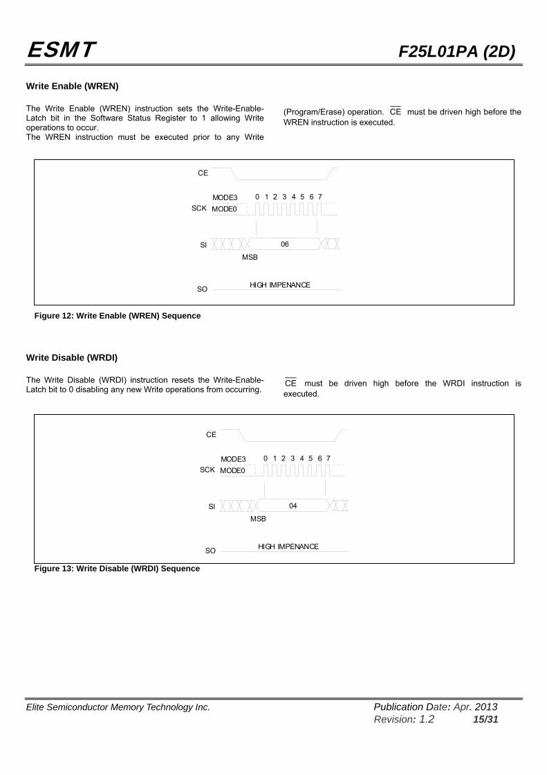
Write Enable (WREN) The Write Enable (WREN) instruction sets the Write-Enable- Latch bit in the Software Status Register to 1 allowing Write operations to occur. The WREN instruction must be executed prior to any Write
(Program/Erase) operation. CE must be driven high before the WREN instruction is executed.
Figure 12: Write Enable (WREN) Sequence
Write Disable (WRDI) The Write Disable (WRDI) instruction resets the Write-Enable- Latch bit to 0 disabling any new Write operations from occurring.
CE must be driven high before the WRDI instruction is executed.
Figure 13: Write Disable (WRDI) Sequence
CE
SCK
SI
0 1 2 3 4 5 6 7
MSB
HIGH IMPENANCESO
06
MODE3MODE0
CE
SCK
SI
0 1 2 3 4 5 6 7
MSB
HIGH IMPENANCESO
04
MODE3MODE0

ESMT F25L01PA (2D)
Elite Semiconductor Memory Technology Inc. Publication Date: Apr. 2013 Revision: 1.2 16/31
Write-Status-Register (WRSR)
The Write Status Register instruction writes new values to the BP2, BP1, BP0, TB and BPL bits of the status register. CE must be driven low before the command sequence of the WRSR instruction is entered and driven high before the WRSR instruction is executed. See Figure 14 for WREN and WRSR instruction sequences. Executing the Write Status Register instruction will be ignored when WP is low and BPL bit is set to “1”. When the WP is low, the BPL bit can only be set from “0” to “1” to lock down the status register, but cannot be reset from “1” to “0”.
When WP is high, the lock-down function of the BPL bit is disabled and the BPL, TB, BP0, BP1,and BP2 bits in the status register can all be changed. As long as BPL bit is set to 0 or WP pin is driven high (VIH) prior to the low-to-high transition of the CE pin at the end of the WRSR instruction, the bits in the status register can all be altered by the WRSR instruction. In this case, a single WRSR instruction can set the BPL bit to “1” to lock down the status register as well as altering the TB, BP0; BP1 and BP2 bits at the same time. See Table 4 for a summary description of WP and BPL functions.
Figure 14: Write-Enable (WREN) and Write-Status-Register (WRSR)
CE
SCK
SI
0 1 2 3 4 5 6 7
MSBMSB
HIGH IMPENANCESO
06
MODE3MODE0
7 6 5 4 3 2 1 001
0 1 2 3 4 5 6 7 8 9 10 11 12 13 14 15
Stauts RegisterData In

ESMT F25L01PA (2D)
Elite Semiconductor Memory Technology Inc. Publication Date: Apr. 2013 Revision: 1.2 17/31
Deep Power Down (DP) The Deep Power Down instruction is for minimizing power consumption (the standby current is reduced from ISB1 to ISB2.). This instruction is initiated by executing an 8-bit command, B9H, and then CE must be driven high. After CE is driven high, the device will enter to deep power down within the duration of TDP.
Once the device is in deep power down status, all instructions will be ignored except the Release from Deep Power Down instruction (RDP) and Read Electronic Signature instruction (RES). The device always power-up in the normal operation with the standby current (ISB1). See Figure 15 for the Deep Power Down instruction.
Figure 15: Deep Power Down Instruction
Release from Deep Power Down (RDP) and Read-Electronic-Signature (RES) The Release form Deep Power Down and Read-Electronic- Signature instruction is a multi-purpose instruction. The instruction can be used to release the device from the deep power down status. This instruction is initiated by driving CE
low and executing an 8-bit command, ABH, and then drive CE high. See Figure 16 for RDP instruction. Release from the deep power down will take the duration of TRES1 before the device will resume normal operation and other instructions are accepted. CE must remain high during TRES1. The instruction also can be used to read the 8-bit Electronic- Signature of the device on the SO pin. It is initiated by driving
CE low and executing an 8-bit command, ABH, followed by 3 dummy bytes. The Electronic-Signature byte is then output from the device. The Electronic-Signature can be read continuously until CE go high. See Figure 17 for RES sequence. After
driving CE high, it must remain high during for the duration of TRES2, and then the device will resume normal operation and other instructions are accepted. The instruction is executed while an Erase, Program or WRSR cycle is in progress is ignored and has no effect on the cycle in progress.
SCK0 1 2 3 4 5 6 7MODE3
MODE0
SI
CE
Standard Current
TDP
MSB
B9
Deep Power Down Current(ISB2)

ESMT F25L01PA (2D)
Elite Semiconductor Memory Technology Inc. Publication Date: Apr. 2013 Revision: 1.2 18/31
Figure 16: Release from Deep Power Down (RDP) Instruction
Figure 17: Read Electronic -Signature (RES) Sequence
Table 6: Electronic Signature Data
Command Electronic Signature Data
RES 10H
SCK0 1 2 3 4 5 6 7MODE3
MODE0
SI
CE
Standby Current
TRES1
MSB
AB
Deep Power Down Current(ISB2)
SOHIGH IMPEDANCE
SCK0 1 2 3 4 5 6 7 8 9MODE3
MODE0
SI
CE
StandbyCurrent
TRES2
MSB
AB
Deep Power Down Current(ISB2)
SOHIGH IMPEDANCE
SS
30 31 32 33 34 35 36 37 38
SS
Electronic-Signature Data OutSSMSB
3 Dummy Bytes
ESMT F25L01PA (2D)
Elite Semiconductor Memory Technology Inc. Publication Date: Apr. 2013 Revision: 1.2 19/31
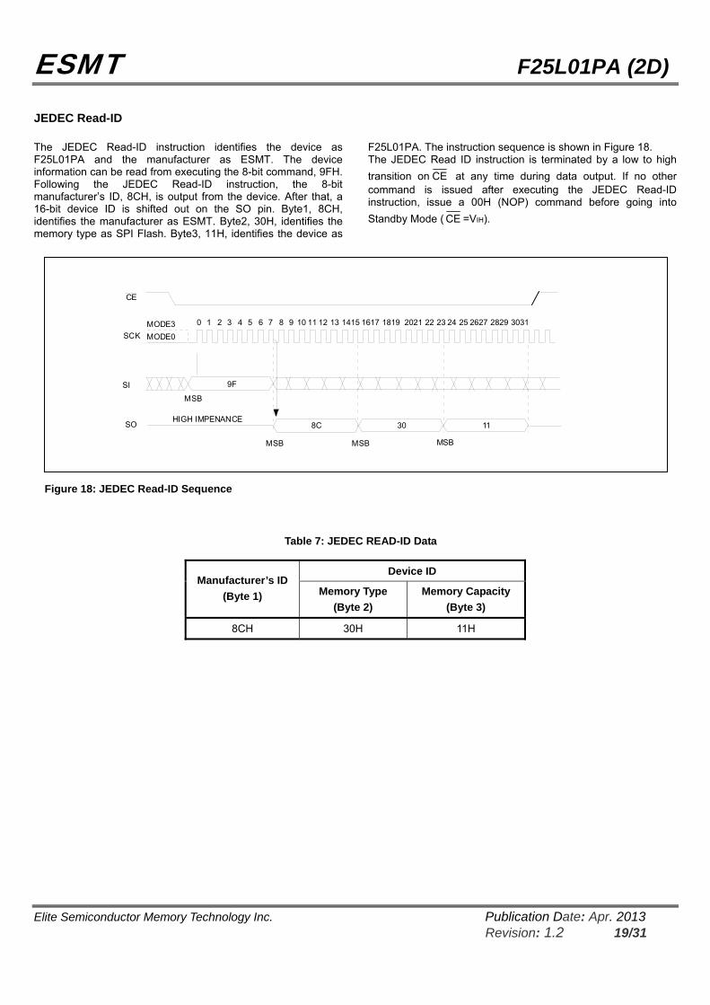
JEDEC Read-ID The JEDEC Read-ID instruction identifies the device as F25L01PA and the manufacturer as ESMT. The device information can be read from executing the 8-bit command, 9FH. Following the JEDEC Read-ID instruction, the 8-bit manufacturer’s ID, 8CH, is output from the device. After that, a 16-bit device ID is shifted out on the SO pin. Byte1, 8CH, identifies the manufacturer as ESMT. Byte2, 30H, identifies the memory type as SPI Flash. Byte3, 11H, identifies the device as
F25L01PA. The instruction sequence is shown in Figure 18. The JEDEC Read ID instruction is terminated by a low to high transition on CE at any time during data output. If no other command is issued after executing the JEDEC Read-ID instruction, issue a 00H (NOP) command before going into Standby Mode ( CE =VIH).
Figure 18: JEDEC Read-ID Sequence
Table 7: JEDEC READ-ID Data
Device ID Manufacturer’s ID
(Byte 1) Memory Type (Byte 2)
Memory Capacity (Byte 3)
8CH 30H 11H
CE
SCK
SIMSB
HIGH IMPENANCESO
9F
MODE3MODE0
0 1 2 3 4 5 6 7 8 9 10 11 12 13 1415 1617 1819 2021 22 23 24 25 2627 2829 3031
8C
MSB
30 11
MSB MSB
ESMT F25L01PA (2D)
Elite Semiconductor Memory Technology Inc. Publication Date: Apr. 2013 Revision: 1.2 20/31
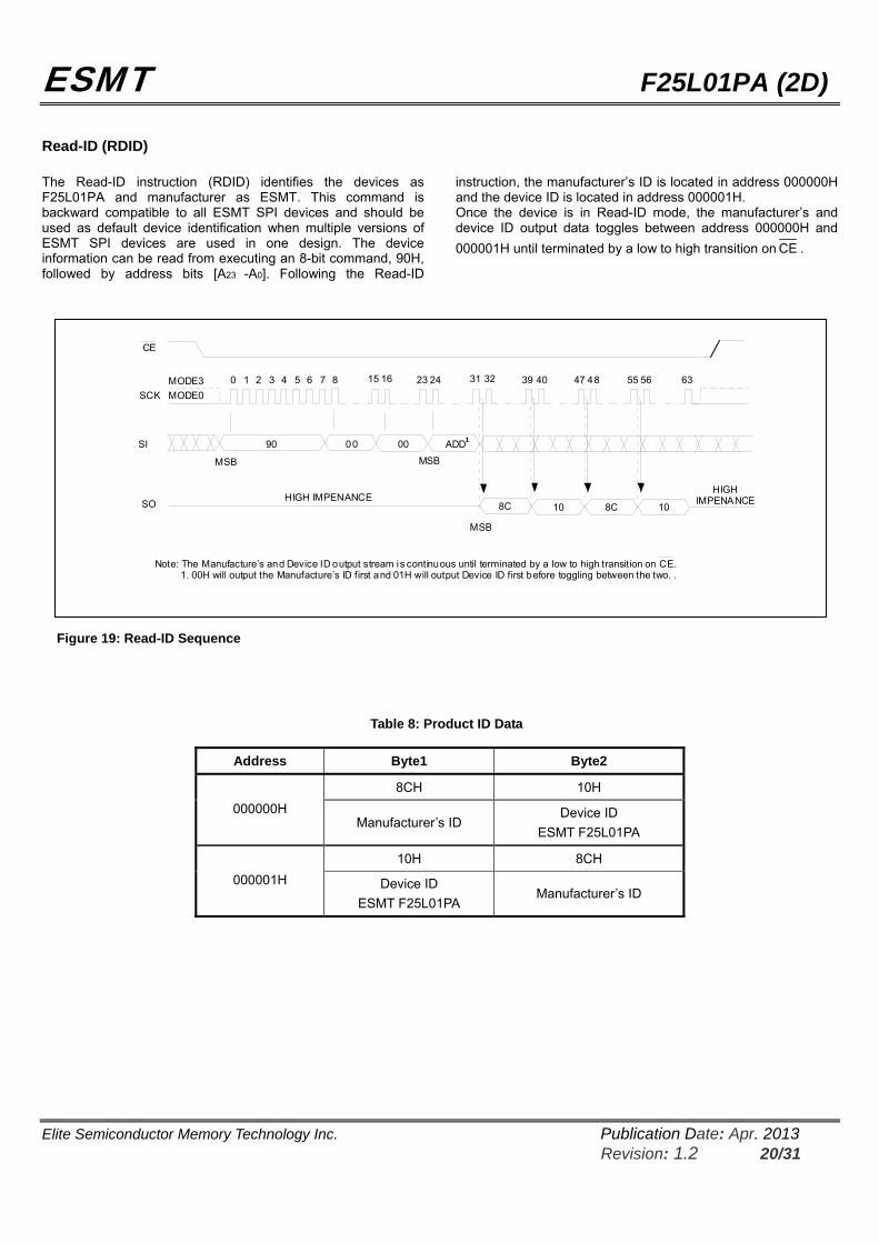
Read-ID (RDID) The Read-ID instruction (RDID) identifies the devices as F25L01PA and manufacturer as ESMT. This command is backward compatible to all ESMT SPI devices and should be used as default device identification when multiple versions of ESMT SPI devices are used in one design. The device information can be read from executing an 8-bit command, 90H, followed by address bits [A23 -A0]. Following the Read-ID
instruction, the manufacturer’s ID is located in address 000000H and the device ID is located in address 000001H. Once the device is in Read-ID mode, the manufacturer’s and device ID output data toggles between address 000000H and 000001H until terminated by a low to high transition on CE .
Figure 19: Read-ID Sequence
Table 8: Product ID Data
Address Byte1 Byte2
8CH 10H 000000H
Manufacturer’s ID Device ID
ESMT F25L01PA
10H 8CH 000001H Device ID
ESMT F25L01PA Manufacturer’s ID
CE
SCK
SI
0 1 2 3 4 5 6 7 8 15 16 23 24 31 32 39 40 47 48 55 56 63
MSBMSB
HIGH IMPENANCESO
90 00 00 ADD1
MODE3MODE0
Note: The Manufacture’s and Device ID output stream is continuous until terminated by a low to high transition on CE.1. 00H will output the Manufacture’s ID first and 01H will output Device ID first before toggling between the two. .
HIGHIMPENANCE8C 8C10 10
MSB
ESMT F25L01PA (2D)
Elite Semiconductor Memory Technology Inc. Publication Date: Apr. 2013 Revision: 1.2 21/31
ELECTRICAL SPECIFICATIONS
Absolute Maximum Stress Ratings (Applied conditions are greater than those listed under “Absolute Maximum Stress Ratings” may cause permanent damage to the device. This is a stress rating only and functional operation of the device at these conditions or conditions greater than those defined in the operational sections of this datasheet is not implied. Exposure to absolute maximum stress rating conditions may affect device reliability.) Storage Temperature . . . . . . . . . . . . . . . . . . . . . . . . . . . . . . . . . . . . . . . . . . . . . . . . . . . . . . . . . . . . . . . . . . . . . . . -65°C to +150°C D. C. Voltage on Any Pin to Ground Potential . . . . . . . . . . . . . . . . . . . . . . . . . . . . . . . . . . . . . . . . . . . . . . . . . . . . . . -0.5V to VDD+0.5V Transient Voltage (<20 ns) on Any Pin to Ground Potential . . . . . . . . . . . . . . . . . . . . . . . . . . . . . . . . . . . . . . . . . . . -2.0V to VDD+2.0V Package Power Dissipation Capability (TA = 25°C) . . . . . . . . . . . . . . . . . . . . . . . . . . . . . . . . . . . . . . . . . . . . . . . . . . 1.0W Surface Mount Lead Soldering Temperature (3 Seconds) . . . . . . . . . . . . . . . . . . . . . . . . . . . . . . . . . . . . . . . . . . . . . 260°C Output Short Circuit Current (Note 1). . . . . . . . . . . . . . . . . . . . . . . . . . . . . . . . . . . . . . . . . . . . . . . . . . . . . . . . . . . . . . 50 mA ( Note 1: Output shorted for no more than one second. No more than one output shorted at a time. ) AC CONDITIONS OF TEST
OPERATING RANGE
Parameter Symbol Value Unit
Operating Supply Voltage VDD 2.7 ~ 3.6 V
Ambient Operating Temperature TA -40 ~ +85 ℃
Table 9: DC OPERATING CHARACTERISTICS
Limits Symbol Parameter Min Max Unit
Test Condition
Standard 10 IDDR1 Read Current @ 33 MHz Dual 15
mA CE =0.1 VDD/0.9 VDD, SO=open
Standard 15 IDDR2 Read Current @ 50MHz Dual 20 mA CE =0.1 VDD/0.9 VDD, SO=open
Standard 17 IDDR3 Read Current @ 86MHz Dual 22 mA CE =0.1 VDD/0.9 VDD, SO=open
IDDR4 Read Current @ 100MHz Standard 22 mA CE =0.1 VDD/0.9 VDD, SO=open
IDDW Program and Erase Current 20 mA CE =VDD ISB1 Standby Current 25 µA CE =VDD, VIN =VDD or VSS ISB2 Deep Power Down Current 10 µA CE =VDD, VIN =VDD or VSS ILI Input Leakage Current ±2 µA VIN=GND to VDD, VDD=VDD Max ILO Output Leakage Current ±2 µA VOUT=GND to VDD, VDD=VDD Max VIL Input Low Voltage -0.5 0.3 x VDD V VDD=VDD Min VIH Input High Voltage 0.7 x VDD VDD +0.4 V VDD=VDD Max VOL Output Low Voltage 0.4 V IOL= 1.6 mA, VDD=VDD Min VOH Output High Voltage VDD-0.2 V IOH=-100 µA, VDD=VDD Min
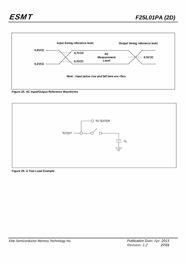
Input Rise/Fall Time . . . . . . . . . . . . . . . . . . . . . . . . . . . . . . . . . . 5 nsOutput Load . . . . . . . . . . . . . . . . . . . . . . . . CL = 15 pF for ≧75MHz. . . . . . . . . . . . . . . . . . . . . . . . . . . . . . . . . . .CL = 30 pF for ≦50MHzSee Figures 25 and 26
ESMT F25L01PA (2D)
Elite Semiconductor Memory Technology Inc. Publication Date: Apr. 2013 Revision: 1.2 22/31
Table 10: CAPACITANCE (TA = 25°C, f=1 MHz, other pins open)
Parameter Description Test Condition Maximum
COUT1 Output Pin Capacitance VOUT = 0V 8 pF
CIN1 Input Capacitance VIN = 0V 6 pF
Note 1: This parameter is measured only for initial qualification and after a design or process change that could affect this parameter.
Table 11: AC OPERATING CHARACTERISTICS
Normal 33MHz Fast 50 MHz Fast 86 MHz Fast 100 MHz UnitSymbol Parameter
Min Max Min Max Min Max Min Max
FCLK Serial Clock Frequency 33 50 86 100 MHz
TSCKH2 Serial Clock High Time 13 9 5 4 ns
TSCKL2 Serial Clock Low Time 13 9 5 4 ns
TCES1 CE Active Setup Time 5 5 5 5 ns
TCEH1 CE Active Hold Time 5 5 5 5 ns
TCHS1 CE Not Active Setup Time 5 5 5 5 ns
TCHH1 CE Not Active Hold Time 5 5 5 5 ns
TCPH CE High Time 100 100 100 100 ns
TCHZ CE High to High-Z Output 6 6 6 6 ns
TCLZ SCK Low to Low-Z Output 0 0 0 0 ns
TDS Data In Setup Time 3 3 3 3 ns
TDH Data In Hold Time 3 3 3 3 ns
THLS HOLD Low Setup Time 5 5 5 5 ns
THHS HOLD High Setup Time 5 5 5 5 ns
ESMT F25L01PA (2D)
Elite Semiconductor Memory Technology Inc. Publication Date: Apr. 2013 Revision: 1.2 23/31
Table 11: AC OPERATING CHARACTERISTICS - Continued
Normal 33MHz Fast 50 MHz Fast 86 MHz Fast 100 MHzSymbol Parameter
Min Max Min Max Min Max Min MaxUnit
THLH HOLD Low Hold Time 5 5 5 5 ns
THHH HOLD High Hold Time 5 5 5 5 ns
THZ3 HOLD Low to High-Z Output 6 6 6 6 ns
TLZ3 HOLD High to Low-Z Output 6 6 6 6 ns
TOH Output Hold from SCK Change 0 0 0 0 ns
TV Output Valid from SCK 12 8 7 7 ns
TWHSL4 Write Protect Setup Time before CE Low 20 20 20 20 ns
TSHWL4 Write Protect Hold Time after CE High 100 100 100 100 ns
TDP3 CE High to Deep Power Down Mode 3 3 3 3 us
TRES13 CE High to Standby Mode ( for DP) 3 3 3 3 us
TRES23 CE High to Standby Mode (for RES) 1.8 1.8 1.8 1.8 us
Note: 1. Relative to SCK. 2. TSCKH + TSCKL must be less than or equal to 1/ FCLK. 3. Value guaranteed by characterization, not 100% tested in production. 4. Only applicable as a constraint for a Write status Register instruction when Block- Protection-Look (BPL) bit is set at 1.
ERASE AND PROGRAMMING PERFORMANCE
Limit Parameter Symbol
Typ2 Max3 Unit
Sector Erase Time TSE 90 250 ms Block Erase Time TBE 0.75 1.5 s Chip Erase Time TCE 1 2 s Write Status Register Time TW 5 15 ms Page Programming Time TPP 1.5 5 ms Erase/Program Cycles1 100,000 - Cycles Data Retention 20 - Years
Notes:
1. Not 100% Tested, Excludes external system level over head. 2. Typical values measured at 25°C, 3V. 3. Maximum values measured at 85°C, 2.7V.
ESMT F25L01PA (2D)
Elite Semiconductor Memory Technology Inc. Publication Date: Apr. 2013 Revision: 1.2 24/31
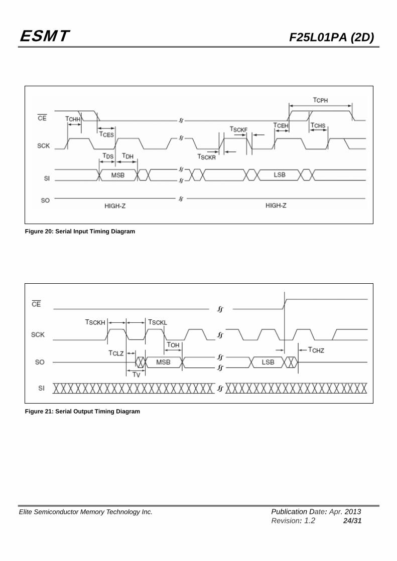
Figure 20: Serial Input Timing Diagram
Figure 21: Serial Output Timing Diagram

ESMT F25L01PA (2D)
Elite Semiconductor Memory Technology Inc. Publication Date: Apr. 2013 Revision: 1.2 25/31
Figure 22: HOLD Timing Diagram
Figure 23: Write Protect setup and hold timing during WRSR when BPL = 1
CE
SCK
SI
HIGH IMPENANCESO
TWHSLTSHWL
WP
ESMT F25L01PA (2D)
Elite Semiconductor Memory Technology Inc. Publication Date: Apr. 2013 Revision: 1.2 26/31
Time
VCC
VCC (max)
VCC (min)
VWI
TPUW
TVSLResetState
Read commandis allowed
Device is fullyaccessible
Program, Erase and Write command is ignored
CE must track VCC
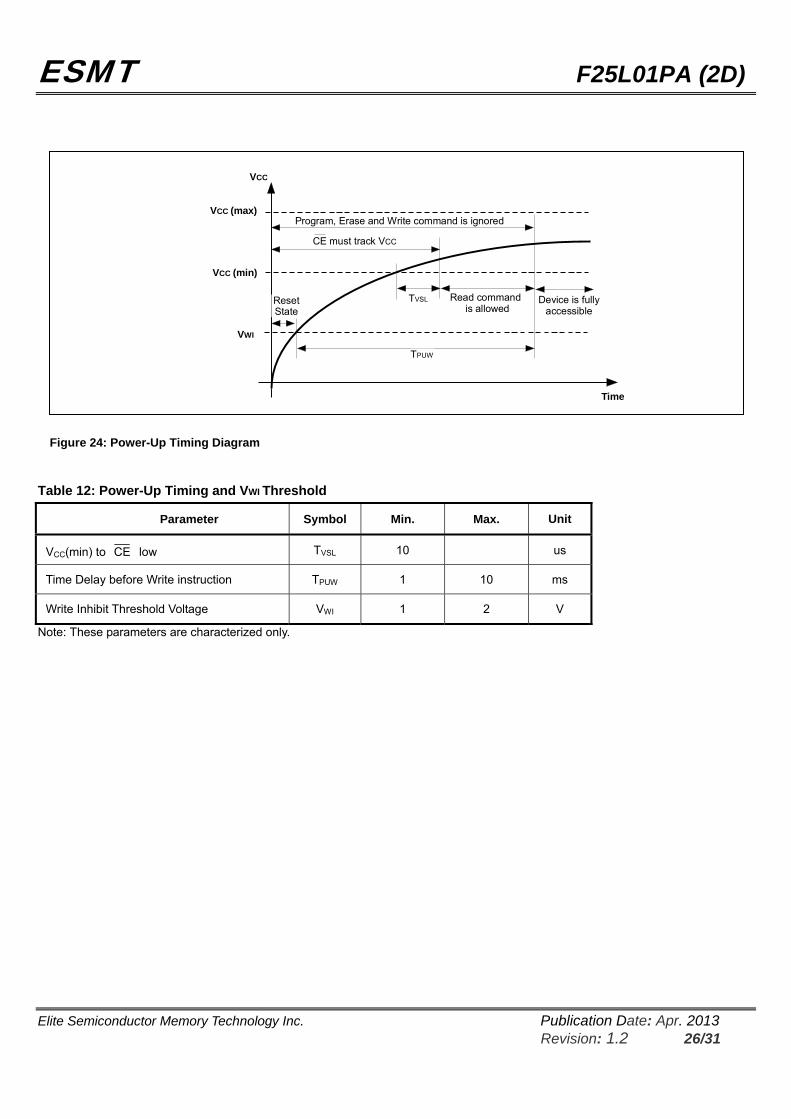
Figure 24: Power-Up Timing Diagram
Table 12: Power-Up Timing and VWI Threshold
Parameter Symbol Min. Max. Unit
VCC(min) to CE low TVSL 10 us
Time Delay before Write instruction TPUW 1 10 ms
Write Inhibit Threshold Voltage VWI 1 2 V
Note: These parameters are characterized only.
ESMT F25L01PA (2D)
Elite Semiconductor Memory Technology Inc. Publication Date: Apr. 2013 Revision: 1.2 27/31
Figure 25: AC Input/Output Reference Waveforms
Figure 26: A Teat Load Example
Input timing reference level Output timing reference level
0.8VCC
0.2VCC
0.7VCC
0.3VCC0.5VCC
ACMeasurement
Level
Note : Input pulse rise and fall time are <5ns
ESMT F25L01PA (2D)
Elite Semiconductor Memory Technology Inc. Publication Date: Apr. 2013 Revision: 1.2 28/31
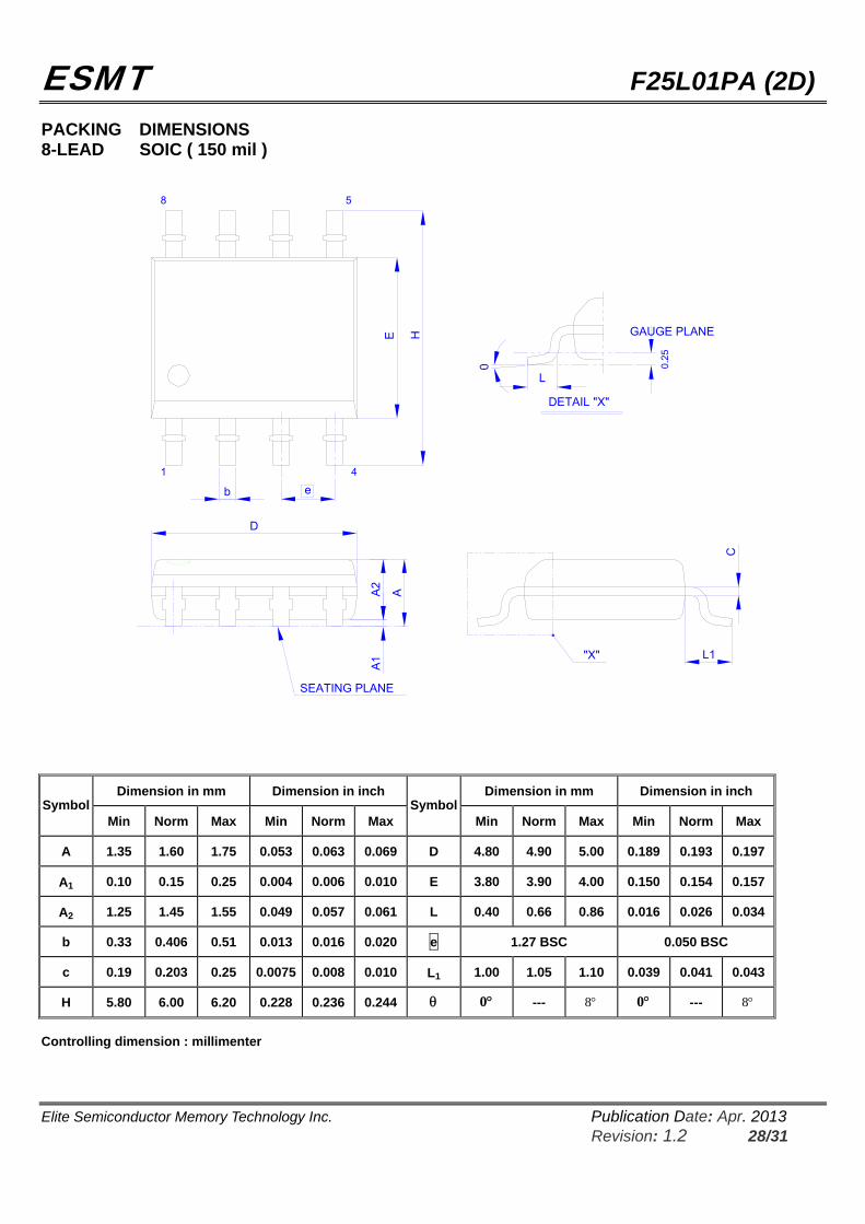
PACKING DIMENSIONS 8-LEAD SOIC ( 150 mil )
b e
0L
DETAIL "X"A
A1
SEATING PLANE
D
A2
L1 "X"
C
1 4
E H
8 5
0.25
GAUGE PLANE
Dimension in mm Dimension in inch Dimension in mm Dimension in inch Symbol
Min Norm Max Min Norm MaxSymbol
Min Norm Max Min Norm Max
A 1.35 1.60 1.75 0.053 0.063 0.069 D 4.80 4.90 5.00 0.189 0.193 0.197
A1 0.10 0.15 0.25 0.004 0.006 0.010 E 3.80 3.90 4.00 0.150 0.154 0.157
A2 1.25 1.45 1.55 0.049 0.057 0.061 L 0.40 0.66 0.86 0.016 0.026 0.034
b 0.33 0.406 0.51 0.013 0.016 0.020 e 1.27 BSC 0.050 BSC
c 0.19 0.203 0.25 0.0075 0.008 0.010 L1 1.00 1.05 1.10 0.039 0.041 0.043
H 5.80 6.00 6.20 0.228 0.236 0.244 θ °0 --- °8 °0 --- °8
Controlling dimension : millimenter
ESMT F25L01PA (2D)
Elite Semiconductor Memory Technology Inc. Publication Date: Apr. 2013 Revision: 1.2 29/31
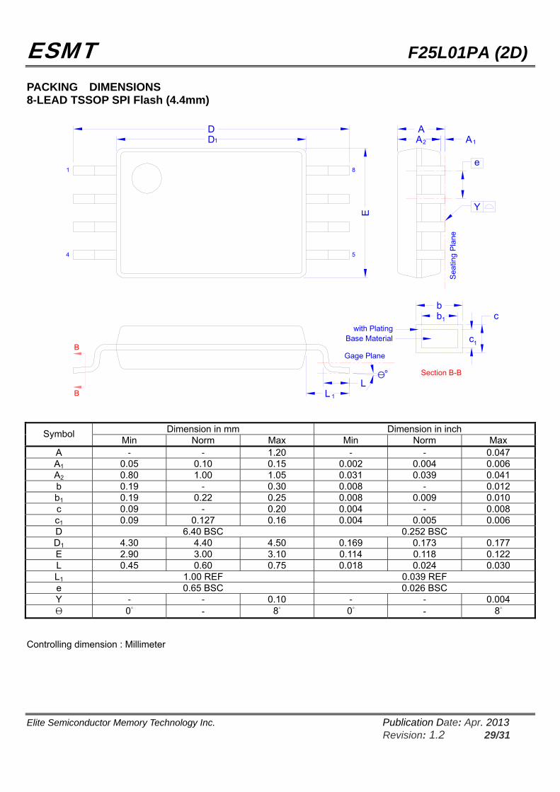
PACKING DIMENSIONS 8-LEAD TSSOP SPI Flash (4.4mm)
1
E
DD
1
4
8
5
e
LL 1
Gage Plane
°
A2 A1
A
Sea
ting
Pla
ne
Y
B
B
bb
1
c
c
1
Section B-B
Base Materialwith Plating
Dimension in mm Dimension in inch Symbol Min Norm Max Min Norm Max
A - - 1.20 - - 0.047 A1 0.05 0.10 0.15 0.002 0.004 0.006 A2 0.80 1.00 1.05 0.031 0.039 0.041 b 0.19 - 0.30 0.008 - 0.012 b1 0.19 0.22 0.25 0.008 0.009 0.010 c 0.09 - 0.20 0.004 - 0.008 c1 0.09 0.127 0.16 0.004 0.005 0.006 D 6.40 BSC 0.252 BSC D1 4.30 4.40 4.50 0.169 0.173 0.177 E 2.90 3.00 3.10 0.114 0.118 0.122 L 0.45 0.60 0.75 0.018 0.024 0.030 L1 1.00 REF 0.039 REF e 0.65 BSC 0.026 BSC Y - - 0.10 - - 0.004 Θ 0° - 8° 0° - 8°
Controlling dimension : Millimeter

ESMT F25L01PA (2D)
Elite Semiconductor Memory Technology Inc. Publication Date: Apr. 2013 Revision: 1.2 30/31
Revision History
Revision Date Description
0.1 2010.11.26 Original
0.2 2010.12.10 Delete speed grade -100
0.3 2011.05.20 1.Add device can support 100MHz in signal output (Max
load capacitance is 15pF) 2.Remove Byte program time
1.0 2011.08.17 Delete “Preliminary”
1.1 2011.09.21 Modify Ambient Operating Temperature
1.2 2013.04.03 1. Correct the description of Block Protection,
Block Protection Lock-Down 2. Correct protection level (0) of block protection table
ESMT F25L01PA (2D)
Elite Semiconductor Memory Technology Inc. Publication Date: Apr. 2013 Revision: 1.2 31/31
Important Notice All rights reserved. No part of this document may be reproduced or duplicated in any form or by any means without the prior permission of ESMT. The contents contained in this document are believed to be accurate at the time of publication. ESMT assumes no responsibility for any error in this document, and reserves the right to change the products or specification in this document without notice. The information contained herein is presented only as a guide or examples for the application of our products. No responsibility is assumed by ESMT for any infringement of patents, copyrights, or other intellectual property rights of third parties which may result from its use. No license, either express, implied or otherwise, is granted under any patents, copyrights or other intellectual property rights of ESMT or others. Any semiconductor devices may have inherently a certain rate of failure. To minimize risks associated with customer's application, adequate design and operating safeguards against injury, damage, or loss from such failure, should be provided by the customer when making application designs.
ESMT's products are not authorized for use in critical applications such as, but not limited to, life support devices or system, where failure or abnormal operation may directly affect human lives or cause physical injury or property damage. If products described here are to be used for such kinds of application, purchaser must do its own quality assurance testing appropriate to such applications.


