
Data Sheet
OXU210HP USB2.0 High-Speed Host, Peripheral and OTG Controller
Features High‐performance, high‐speed USB dual‐role (host/peripheral) controller
Compatible with the Universal Serial Bus Specification, Revision 2.0 for high‐speed (480 Mb/s), full‐speed (12 Mb/s), and low‐speed (1.5 Mb/s) operations
High‐speed optimized host controller with transaction translator for complete backward compatibility with full‐speed and low‐speed products
Two high‐speed USB ports; one port remains host while the other can be configured as peripheral, host, or OTG (dual role)
Simultaneous operation of both ports
Processor interface is either 16 bits (BGA) or configurable 16 or 32 bits (LQFP)
Fast microprocessor access cycle and double/multi buffering support for USB transfers
Host interface contains support for common SoC DMA modes including bursting and slave request/acknowledge protocols
Complete host, peripheral and OTG software solutions for popular microprocessors using many of the most popular operating systems
Advanced power management controls chip clocking and PHY function for very low power consumption
Integrated on‐chip VBUS voltage comparator and 100 mA charge pump
72 Kbytes of single‐port SRAM provides space for data structures and buffer space for transfer data
True transfer level operation, with transaction scheduling and handling (data sequence toggle, error retry, etc.), implemented in hardware
Integrated PLL runs from a single 12‐MHz crystal or an external 12‐MHz clock source
DS-0037 Dec 06 External—Free Release 1

OXU210HP Data Sheet Oxford Semiconductor, Inc.
Packaging7×7 mm BGA, 84‐ball, RoHS compliant14×14 mm LQFP, 128‐pin, RoHS compliant
Operating temperature range: ‐40° to 85° C
Device Overview
The Oxford Semiconductor OXU210HP is a single‐chip, high‐speed USB host and high‐speed USB peripheral controller with integrated transceivers. It is the fourth controller in the family of integrated low‐cost, high‐performance, OTG controllers that have been specifically designed for embedded systems.
The OXU210HP operates at up to 480 Mb/s, using a compatible EHCI‐based core. It also includes an integrated transaction translator that supports full‐speed (12 Mb/s) and low‐speed (1.5 Mb/s) USB peripherals.
The selectable 16‐ and 32‐bit processor interface is compatible with a variety of CPUs. A large 72‐Kbyte buffer has also been integrated to reduce interrupts and minimize CPU overhead.
The OXU210HP supports all USB transfer modes (control, interrupt, bulk and isochronous) and is supported with USB device drivers and the Oxford Semiconductor USBLink product suite. The USBLink host, peripheral and OTG stacks have been ported to a wide variety of real time operating systems including VxWorks®, ThreadX®, and Nucleus®.
In addition, Oxford Semiconductor also makes available low‐level controller drivers for other native USB stacks such as those included with Windows® CE and Linux® 2.6.x.
2 External—Free Release DS-0037 Dec 06
Oxford Semiconductor, Inc. OXU210HP Data Sheet
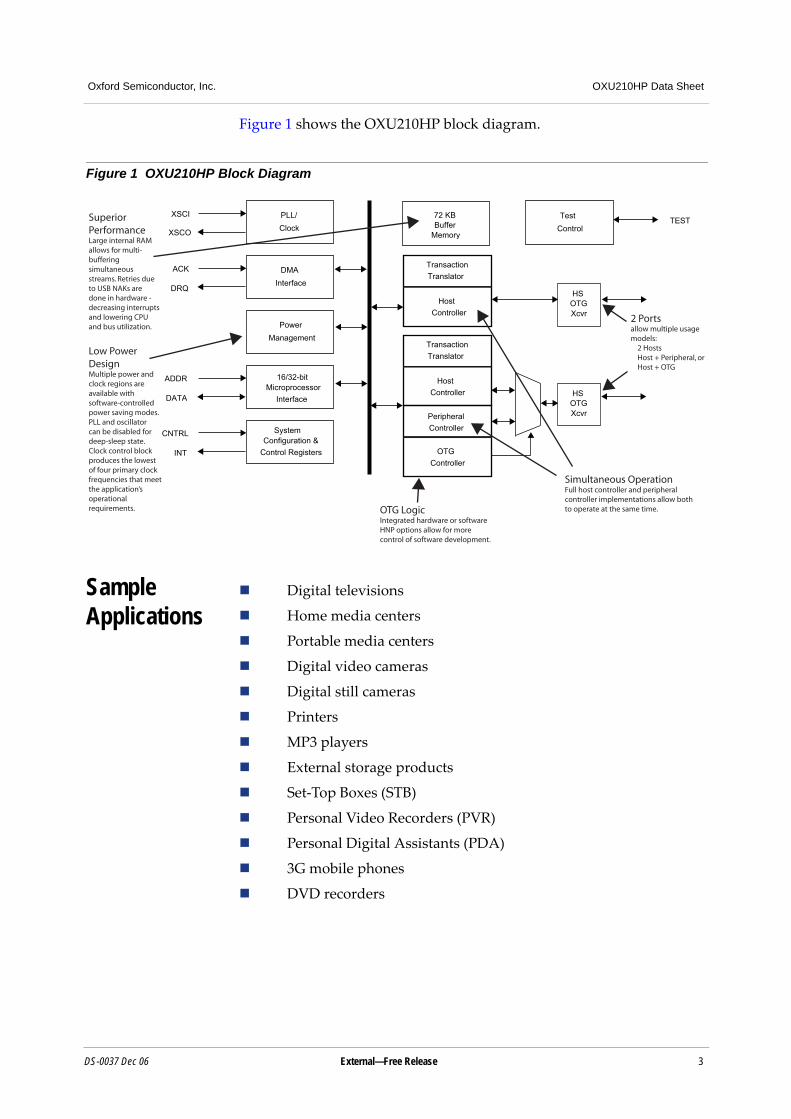
Figure 1 shows the OXU210HP block diagram.
Figure 1 OXU210HP Block Diagram
Sample Applications
Digital televisions
Home media centers
Portable media centers
Digital video cameras
Digital still cameras
Printers
MP3 players
External storage products
Set‐Top Boxes (STB)
Personal Video Recorders (PVR)
Personal Digital Assistants (PDA)
3G mobile phones
DVD recorders
XSCI PLL/ Clock XSCO
ACK DMA Interface DRQ
Power Management
ADDR
DATA
CNTRL
INT
16/32-bit Microprocessor
Interface
System Configuration &
Control Registers
72 KB
Memory Buffer
Transaction Translator
Host Controller
Transaction Translator
Host Controller
Peripheral Controller
OTG Controller
Test Control
HS
Xcvr OTG
HS
Xcvr OTG
TEST
2 Portsallow multiple usagemodels: 2 Hosts Host + Peripheral, or Host + OTG
SuperiorPerformanceLarge internal RAMallows for multi-bufferingsimultaneousstreams. Retries dueto USB NAKs aredone in hardware -decreasing interruptsand lowering CPUand bus utilization.
Low PowerDesignMultiple power andclock regions areavailable withsoftware-controlledpower saving modes.PLL and oscillatorcan be disabled fordeep-sleep state.Clock control blockproduces the lowestof four primary clockfrequencies that meetthe application’soperationalrequirements. OTG Logic
Integrated hardware or softwareHNP options allow for morecontrol of software development.
Simultaneous OperationFull host controller and peripheralcontroller implementations allow bothto operate at the same time.
DS-0037 Dec 06 External—Free Release 3

OXU210HP Data Sheet Oxford Semiconductor, Inc.
Development Support
The OXU210HP product suite includes the USB controller as well as the protocol stacks and the driver software that enable a wide variety of USB applications. This unique ability to deliver a total hardware and software solution sets Oxford Semiconductor apart from other semiconductor companies and benefits customers by:
Shortening time to market
Reducing risk
Offering a single source for hardware and software, thereby reducing the number of suppliers the customer has to deal with
Oxford Semiconductor is a Microsoft® Windows® Embedded Partner and has developed host and peripheral controller drivers for Windows CE 5.0. Similar software support is also available for Linux® 2.6.x.
For customers using an RTOS such as VxWorks®, ThreadX®, Nucleus®, OSE, LynxOS®, and AMXTM, among others, Oxford Semiconductor offers its USBLinkTM host, peripheral and On‐The‐Go software solutions.
The USBLink Product Suite is a modularized approach to providing USB connectivity for a wide variety of embedded products. Due to its flexible architecture and broad based support for USB host, peripheral and OTG applications, Oxford Semiconductor can tailor the USBLink software deliverables to meet each customer’s USB requirements.
The USBLink solutions are configurable and can support systems with:
Big or little endian processors
DMA or non‐DMA USB controllers
A wide variety of USB controllers, including the OXU210HP
Complex to simple operating systems
Oxford Semiconductor has over eight years of experience developing embedded USB technology. Its USBLink software has been ported to twenty different operating systems and a wide variety of embedded architectures. USBLink is shipping in many millions of units.
4 External—Free Release DS-0037 Dec 06

Oxford Semiconductor, Inc. OXU210HP Data Sheet
Electrical Characteristics
Table 1 to Table 10 detail the required operating conditions for the device and the DC and AC electrical characteristics.
Note: 1 Permanent device damage may occur if absolute maximum ratings are exceeded. Functional operation should be restricted to the normal operating conditions specified in the following section. Exposure to absolute maximum rating conditions for extended periods may affect device reliability.
Table 1 Absolute Maximum Device Ratings
Symbol Parameter Condition Min Max UnitVPWM3, VDD3IO
3.3 V digital power supply -0.3 4.0 V
VDD3.3A 3.3 V analog power supply -0.3 4.0 V
VDD1.8 1.8 V power supply -0.3 2.16 V
VIO 1.65 V to 3.3 V power supply
-0.3 4.0 V
VI DC input voltage -0.3 4.0 V
TS Storage temperature -40 +150 °C
Table 2 Recommended Operating Conditions
Symbol Parameter Condition Min Max UnitVPWM3, VDD3IO
3.3 V digital power supply 3.0 3.6 V
VDD3.3A 3.3 V analog power supply 3.0 3.6 V
VDD1.8 1.8 V power supply 1.62 1.98 V
VIO 1.65 - 3.3 Vwide-range I/O power supply
1.65 3.6 V
VI3.3 DC input voltage of 3.3 V pins 0 3.6 V
VIW DC input voltage of wide-range pins 0 VIO + 0.3 V
TO Operating temperature -40 +85 °C
Table 3 DC Characteristics, Full-Speed USB I/O Signals: DP_HOST, DM_HOST, DP_OTG, DM_OTG
Symbol Parameter Condition Min Max UnitVDI Diff. input sensitivity |VI(DP) – VI(DM)| 0.2 -- V
VCM Diff. comm. mode range 0.8 2.5 V
VOL Static output low -- 0.3 V
VOH Static output high 2.8 3.6 V
VCRS Output signal crossover 1.3 2.0 V
CIN Input capacitance 20 pF
DS-0037 Dec 06 External—Free Release 5

OXU210HP Data Sheet Oxford Semiconductor, Inc.
Note: 1 The charge pump supply VCPSUPPLY supplies the external components of the charge pump circuit. This is not a pin on the chip.
Table 4 DC Characteristics, High-Speed USB I/O Signals: DP_HOST, DM_HOST, DP_OTG, DM_OTG
Symbol Parameter Condition Min Max UnitVHSDIFF High-speed differential input
sensitivity|VI(DP) – VI(DM)| 300 -- mV
VHSCM High-speed data signaling common mode range
-50 500 mV
VHSSQ High-speed squelch detection threshold
Squelch detected -- 100 mVNo squelch detected 150 -- mV
VHSOI High-speed idle output voltage (differential)
-10 10 mV
VHSOL High speed low level output voltage (differential)
-10 10 mV
VHSOH High speed high level output voltage (differential)
-360 400 mV
VCHIRPJ Chirp-J output voltage (differential)
700 1100 mV
VCHIRPK Chirp-K output voltage (differential)
-900 -500 mV
Table 5 DC Characteristics, Logic Signals
Symbol Parameter Condition Min Max UnitVOL Low level output voltage -- 0.4 V
VOH High level output voltage VIO = 3.3 V 2.4 -- V
VIO = 2.5 V 1.85 -- V
VIO = 1.8 V 0.75 * VIO
VIL Low level input voltage VIO = 3.3 V -- 0.8 V
VIO = 2.5 V -- 0.25 * VIO V
VIO = 1.8 V 0.3 * VIO --
VIH High level input voltage VIO = 3.3 V 2.0 -- V
VIO = 2.5 V 0.625 * VIO -- V
VIO = 1.8 V 0.7 * VIO --
CIN Input capacitance 2.2 (typical) pF
COUT Output capacitance 2.2 (typical) pF
CBI Bi-directional capacitance 2.2 (typical) pF
IIN Input leakage current No pull up or pull down -10 10 µA
6 External—Free Release DS-0037 Dec 06

Oxford Semiconductor, Inc. OXU210HP Data Sheet
Table 6 DC Characteristics, ID Resistance
Symbol Parameter Condition Min Max UnitRB-PLUG-ID Resistance to ground on
Mini-B plug100 K -- Ω
RA-PLUG-ID Resistance to ground on Mini-B plug
-- 10 Ω
Table 7 DC Characteristics, Charge Pump
Symbol Parameter Condition Min Max UnitCVout Output voltage Driving current <= 100 mA 4.75 5.07 V
CIdrive Driving current VCPSUPPLY = 3.3 VOutput voltage = 5 V
-- 100 mA
Ctst Start-up time when enabled VCPSUPPLY = 3.3 VRVout = 4.5 V (90%)
400 (typical) µs
Table 8 AC Characteristics, DP_HOST, DM_HOST, DP_OTG, DM_OTG Driver Characteristics (High Speed)
Symbol Parameter Condition Min Max UnittHSRt High speed differential rise
time500 -- ps
tHSF High speed differential fall time
500 -- ps
RDRV Driver output impedance Equivalent resistance used as internal chip
40.5 49.5 Ω
Table 9 AC Characteristics, DP_HOST, DM_HOST, DP_OTG, DM_OTG Driver Characteristics (Full Speed)
Symbol Parameter Condition Min Max UnittFR Rise time CL = 50 pF 4 20 ns
tFF Fall time CL = 50 pF 4 20 ns
tFRFM TR/TF matching 90 110 %
ZDRV Driver output resistance Steady state drive with external 33 Ω series resistor
3 9 Ω
Table 10 AC Characteristics, DP_HOST, DM_HOST, DP_OTG, DM_OTG Driver Characteristics (Low Speed)
Symbol Parameter Condition Min Max UnittLR Rise time CL = 200 - 600 pF 75 300 ns
tFF Fall time CL = 200 - 600 pF 75 300 ns
tFRFM TR/TF matching 80 125 %
DS-0037 Dec 06 External—Free Release 7

OXU210HP Data Sheet Oxford Semiconductor, Inc.
Power Consumption
Table 11 gives the power consumption figures for the OXU210HP.
The above measurements are at typical process corner and room temperature and do not account for process and temperature variations. Bulk transfer current measurements are made at the peak of each transfer. Actual average current in customer application will be lower. Transmit of test packet measurements are taken in test mode and represent maximum switching on the bus.
Table 11 OXU210HP Power Consumption
Mode 3.3 V (mA) 1.8 V (mA) Power (mW)Full-power down 0.06 0.2 0.56Power down, remote wakeup enabled (PHY PLL enabled during power down)
0.66 0.24 2.61
Idle but clocking @ 120 MHz (port suspend) 23 56 177FS bulk in/out transfers @ OTG port, peak current (120 MHz), SPH idle 33 60 217FS transmit of test packet, both ports (60 MHz) 25 35 146HS bulk in/out transfers @ OTG port, peak current (120 MHz), SPH idle 61 70 327HS transmit of test packet, OTG port only (120 MHz) 56 59 291HS transmit of test packet, both ports (120 MHz) 91 59 407
8 External—Free Release DS-0037 Dec 06

Oxford Semiconductor, Inc. OXU210HP Data Sheet
Pin Layout The device is supplied as a 128‐pin LQFP package and as an 84‐ball BGA package. Figure 2 shows the chip layout of the 128‐pin LQFP package. Figure 3 shows the chip layout of the 84‐ball BGA package.
Figure 2 OXU210HP 128-Pin LQFP Package (Top View)
PD
_PM
OS
DEB
UG
1
BE3
40 41 42
33 34 35 36 37 38 39
43 44 45 46 47 48 49 50 51 52 53 54 55 56 57 58 59 60 61 62
64 63
D 15 D 16
D 17
D 18 D 19 D 20
D 21 D 22 D 23 BE0 BE1 BE2
VSSA VDD3.3A DP_HOST DM_HOST REF_HOST
XSCI
VSSA VDD3.3A VDD1.8 VDD1.8 VSS VSS
XSCO VDD3.3A VSSA REF_OTG DM_OTG DP_OTG
AC
K0
AC
K1
GP
IO0
V SS
V IO
DR
Q0
TEST
DEB
UG
3
DEB
UG
2
DEB
UG
0
/INT
/R
ES
ET
V IO
V SS
V DD
1.8
V SS
/PO
/OC
/E
XV
BO
V D
D3I
O
V SSA
VO
UT
DR
Q1
V SSA
V D
D3.
3A
VB
US
V PW
M3
EX
T
V SSA
9
D29
88
10
D30
87
11
D31
86
12
V IO
85
13
V SS
84
14
D0
15
D1
82
17
D3
80
18
VD
D1.
8
79
19
D4
78
20
D5
77
21
D6
76
22
D7
75
23
D8
74
24
D9
73
25
D10
72
16
D2
81
26
D11
71
27
V IO
70
28
V SS
69
29
V SS
68
30
D12
67
31
D13
66
32
D14
65 D
28
89
7
V SS
90
6
V IO
91
5
D27
92
4
D26
93
3
D25
94
2
D24
95
1
/RD
96
121 120 119
128 127 126 125 124 123 122
118 117 116 115 114 113 112 111 110 109 108 107 106 105 104 103 102 101 100 99
97 98
VSS /WR /CS A 16 A 15 A 14
VIO
VSS VDD1.8
A5 A4 A3 A2 A1
VSS
DEBUG 5
DEBUG 4 GPIO3 GPIO2 GPIO1
DEBUG 6
DEBUG 7
VIO
A6 A7 A8
A9 A 10 A 11 A 12 A 13
83 VDD3.3A
VSS
8
ID
LQBG
DS-0037 Dec 06 External—Free Release 9

OXU210HP Data Sheet Oxford Semiconductor, Inc.
Table 12 lists the LQFP pin allocations.
Table 12 OXU210HP 128-Pin LQFP Pin Allocations (Sheet 1 of 2)
Pin No. Bits
Type(1) Name Description
Processor Interface (61 pins)14, 15, 16, 17, 19, 20, 21, 22, 23, 24, 25, 26, 30, 31, 32, 33
16 MSBCT D0 - D15 16-bit data bus
2, 3, 4, 5, 8, 9, 10, 11, 34, 35, 36, 37, 38, 39, 40, 41
16 MSBCT D16 - D31 Additional 16-bits of data bus for optional 32-bit mode. In 16-bit mode, these signals have an internal pull down
106, 107, 108, 109, 110, 111, 112, 113, 116, 117, 118, 119, 120, 123, 124, 125
16 MSI A1 - A16 Address bus for direct address space of 72 Kbytes plus memory mapped registers
127 1 MSIU /WR Write strobe1 1 MSIU /RD Read strobe126 1 MSIU /CS Chip select83 1 MOCT /INT Interrupt to the MCU.This pin can be software
configured as a driven output or WO. WO is the default
84 1 I /RESET Hardware reset
90, 91 2 MOCT DRQ1, DRQ0 DMA request outputs to support two channels
92, 93 2 SI ACK1, ACK0 DMA acknowledge
42, 43 2 MSI BE0, BE1 Byte enables
44, 45 2 MSID BE2, BE3 Byte enables. These signals have an internal pull down.
General Purpose I/O (4 pins)96, 97, 98, 99 4 BC GPIO0 - GPIO3 General purpose I/O
Power and Ground (38 pins)7, 13, 28, 29, 55, 56, 79, 82, 95, 105, 115, 122, 128
13 VSS Digital ground
46, 51, 60, 65, 68, 73
6 VSSA Analog ground
18, 53, 54, 81, 114
5 VDD1.8 1.8 V core power. VREGOUT may be used for the supplies
47, 52, 59, 64, 72 5 VDD3.3A Analog +3.3 V power
6, 12, 27, 80, 94, 104, 121
7 VIO Wide-range I/O voltage. If using +1.8 V, VREGOUT may be used for the supplies
74 1 VDD3IO Digital +3.3 V power
10 External—Free Release DS-0037 Dec 06

Oxford Semiconductor, Inc. OXU210HP Data Sheet
67 1 VPWM3 Analog 3.3 V power for the charge pump Pulse Width Modulator (PWM)
USB Interface (9 pins)48, 49 2 B DP_HOST, DM_HOST Data lines for host port. If not used, these pins should
be left floating62, 63 2 B DP_OTG, DM_OTG Data lines for OTG port. If not used, these pins
should be left floating71 1 5I VBUS VBUS input used by the voltage comparators of the
OTG port for connection. This pin should be left floating in a host-only application
75 1 P5O /EXVBO Turn on/off the external VBUS (5 V) for OTG operation (1:VBUS off, 0: VBUS on) when using the external VBUS source
76 1 P5IU /OC Over current condition indicator for powered host ports
77 1 P5IU ID Connected to the ID pin of the mini-AB connector for OTG applications. With the help of an internal pull-up resistor, this pin determines the chip’s responsibility in an OTG application (0: A-device, 1:B-device)
78 1 P5OT /PO Turn on/off gang power for all host portsClock Interface (2 pins)57 1 I XSCI Input. A 12 MHz passive crystal should be connected
across the two pins (XSCI and XSCO). Optionally, a 12 MHz oscillator can be sourced through XSCI while keeping XSCO unconnected
58 1 O XSCO OutputInternal VBUS Charge Pump (3 pins)
69 1 O PD_PMOS Internal charge pump output for P-MOSFET (optional switch on the VOUT)
66 1 O EXT Internal charge pump output for N-MOSFET70 1 I VOUT Internal charge pump output voltage feedback pin
Test (9 pins)85, 86, 87, 88, 100, 101, 102, 103
8 OC DEBUG0 - DEBUG7 Debug outputs
89 1 I TEST Factory test mode. This pin should be grounded or left floating (has an internal pull-down) for normal operation
Miscellaneous (2 pins)50 1 B REF_HOST Connect external reference resistor (12 KW +/‐
1%) to VSSA. One per port61 1 B REF_OTG
Table 12 OXU210HP 128-Pin LQFP Pin Allocations (Sheet 2 of 2)
Pin No. Bits
Type(1) Name Description
DS-0037 Dec 06 External—Free Release 11

OXU210HP Data Sheet Oxford Semiconductor, Inc.
Note to Table 12: 1 Type key: format is [(L)(W_)X(Y)(_Z(T))] where the following conventions apply:
2 Program to OD or 3.3 V CMOS via the ASO register (0x0068).3 Program to 3.3, 2.5, or 1.8 V by setting the VIO voltage level.4 Program to 2 mA, 4 mA, 6 mA, or 8 mA via the I/O Control register (0x006C).
L—Logic Level W—Tolerance X—Type Y—Pull Z—Drive T—Tristate
P(2) OD3.3 CMOS
5 5 V I Input U Pull up C(4) T Tristate
M(3) Multi-voltage:3.3 V CMOS2.5 V CMOS1.8 V CMOS
3.3 V O Output D Pull down Normal
S Schmitt Trigger B Bidirectional None
12 External—Free Release DS-0037 Dec 06

Oxford Semiconductor, Inc. OXU210HP Data Sheet
Figure 3 OXU210HP 84-Ball BGA Package (Top View)
1 2 3 4 5 6 7 8 9 10
A /CS A 15 A 13 A 11 A 10 A 7 A 6 A 4 A 2 ACK0
B /RD /WR A 14 A 12 A 9 A 8 A 5 A 3 GPIO0 DRQ0
C D 0 A16 VSS VIO VSS VDD1.8 VSS VDD1.8 A 1 TEST
D D 1 D 2 VSS VIO /INT /RESET
E D 3 D 4 VDD1.8 VSS ID /PO
F D6 D 5 D7 VSSA /EXVBO /OC
G D 8 D 9 VSS VDD3.3A VBUS VOUT
H D 11 D 10 VSSA VDD3.3A VDD3.3A VDD3.3A VSSA VSSA VPWM3 PD_PMOS
J D 13 D 12 BE 1 BE 0 VSSA VDD3IO VIO VDD3.3A VSSA EXT
K D 15 D 14 DM_HOST DP_HOST REF_HOST XSCI XSCO DM_OTG DP_OTG REF_OTG
OXU210HP-TBBG
DS-0037 Dec 06 External—Free Release 13

OXU210HP Data Sheet Oxford Semiconductor, Inc.
Table 13 lists the BGA pin allocations.
Table 13 OXU210HP 84-Ball BGA Pin Allocations (Sheet 1 of 2)
Pin No. Bits
Type(1) Name Description
Processor Interface (41 pins)C1, D1, D2, E1, E2, F2, F1, F3, G1, G2, H2, H1, J2, J1, K2, K1
16 MSBCT D0 - D15 16-bit data bus
C9, A9, B8, A8, B7, A7, A6, B6, B5, A5, A4, B4, A3, B3, A2, C2
16 MSI A1 - A16 Address bus for direct address space of 72 Kbytes plus memory mapped registers
B2 1 MSIU /WR Write strobeB1 1 MSIU /RD Read strobeA1 1 MSIU /CS Chip selectD9 1 MOCT /INT Interrupt to the MCU.This pin can be software configured
as a driven output or WO. WO is the defaultD10 1 I /RESET Hardware resetB10 1 MOT DRQ0 DMA request outputs to support two channels
A10 1 SI ACK0 DMA acknowledge
J4, J3 2 MSI BE0, BE1 Byte enables
General Purpose I/O (1 pin)B9 1 B GPIO0 General purpose I/O
Power and Ground (25 pins)C3, C5, C7, D3, E8, G3
6 VSS Digital ground
F8, H3, H7, H8, J5, J9 6 VSSA Analog ground
C6, C8, E3 3 VDD1.8 1.8 V core power. VREGOUT may be used for the supplies
G8, H4, H5, H6, J8 5 VDD3.3A Analog +3.3 V power
C4, D8, J7 3 VIO Wide-range I/O voltage. If using +1.8 V, VREGOUT may be used for the supplies
J6 1 VDD3IO Digital +3.3 V power
H9 1 VPWM3 Analog 3.3 V power for the charge pump Pulse Width Modulator (PWM)
USB Interface (9 pins)K4, K3 2 B DP_HOST, DM_HOST Data lines for host port. If not used, these pins should be
left floatingK8, K9 2 B DM_OTG, DP_OTG Data lines for OTG port. If not used, these pins should be
left floating.G9 1 5I VBUS VBUS input used by the voltage comparators of the OTG
port for connection. This pin should be left floating in a host only application
14 External—Free Release DS-0037 Dec 06

Oxford Semiconductor, Inc. OXU210HP Data Sheet
Note to Table 13: 1 Type key: format is [(L)(W_)X(Y)(_Z(T))] where the following conventions apply:
2 Program to OD or 3.3 V CMOS via the ASO register (0x0068).3 Program to 3.3, 2.5, or 1.8 V by setting the VIO voltage level.4 Program to 2 mA, 4 mA, 6 mA, or 8 mA via the I/O Control register (0x006C).
F9 1 P5O /EXVBO Turn on/off the external VBUS (5 V) for OTG operation (1:VBUS off, 0:VBUS on) when using the external charge pump
F10 1 P5IU /OC Over current condition indicator for powered host portsE9 1 P5IU ID Connected to the ID pin of the mini-AB connector for
OTG applications. With the help of an internal pull-up resistor, this pin determines the chip’s responsibility in an OTG application (0: A-peripheral, 1:B-peripheral)
E10 1 P5O /PO Turn on/off the gang power for all host portsClock Interface (2 pins)K6 1 I XSCI Input. A 12 MHz passive crystal should be connected
across the two pins (XSCI and XSCO). Optionally, a 12 MHz oscillator can be connected to XSCI while keeping XSCO unconnected
K7 1 O XSCO OutputInternal VBUS Charge Pump (3 pins)
H10 1 O PD_PMOS Internal charge pump output for P-MOSFET (optional switch on the VOUT)
J10 1 O EXT Internal charge pump output for N-MOSFETG10 1 I VOUT Internal charge pump output voltage feedback pin
Test (1 pin)C10 1 SIUC TEST Factory test mode. This pin should be grounded or left
floating (has an internal pull-down) for normal operationMiscellaneous (2 pins)K5 1 B REF_HOST Connect external reference resistor (12 KΩ +/- 1%) to
VSSA. One per portK10 1 B REF_OTG
Table 13 OXU210HP 84-Ball BGA Pin Allocations (Sheet 2 of 2)
Pin No. Bits
Type(1) Name Description
L—Logic Level W—Tolerance X—Type Y—Pull Z—Drive T—Tristate
P(2) OD3.3 CMOS
5 5 V I Input U Pull up C(4) T Tristate
M(3) Multi-voltage:3.3 V CMOS2.5 V CMOS1.8 V CMOS
3.3 V O Output D Pull down Normal
S Schmitt Trigger B Bidirectional None
DS-0037 Dec 06 External—Free Release 15

OXU210HP Data Sheet Oxford Semiconductor, Inc.
Package Layout
Figure 4 shows the package layout for the 128‐pin LQFP package. Figure 5 on page 17 shows the layout for the 84‐ball TFBGA.
Figure 4 128-Pin LQFP
16 External—Free Release DS-0037 Dec 06

Oxford Semiconductor, Inc. OXU210HP Data Sheet
Figure 5 84-Ball TFBGA Package
Ordering Information
The following conventions are used to identify Oxford Semiconductor products:
OXU210HP - LQBG
Revision
Package Type: LQ 128-Pin LQFP
Part Number
Green (RoHS compliant)
OXU210HP - TBBG
Revision
Package Type: TB 84-Ball TF-BGA
Part Number
Green (RoHS compliant)
DS-0037 Dec 06 External—Free Release 17
OXU210HP Data Sheet Oxford Semiconductor, Inc.
© Oxford Semiconductor, Inc. 2006
The content of this document is furnished for informational use only, is subject to change without notice, and should not be construed as a commitment by Oxford Semiconductor, Inc. Oxford Semiconductor, Inc. assumes no responsibility or liability for any errors or inaccuracies that may appear in this document.
USBLink is a trademark of Oxford Semiconductor, Inc.VxWorks is a registered trademark of Wind River Systems.ThreadX is a registered trademark of Express Logic, Inc.
Nucleus is a registered trademark of Mentor Graphics Corporation.Windows is a trademark of Microsoft, Inc., registered in the US and other countries.
LynxOS is a registered trademark of LynuxWorks, Inc.AMX is a trademark of KADAK Products LTD.Linux is a registered trademark of Linus Torvalds.
All other trademarks are the property of their respective owners.
Contacting Oxford Semi-conductor
See the Oxford Semiconductor website (http://www.oxsemi.com) for further detail about Oxford Semiconductor devices, or email [email protected].
Revision Information
Table 14 documents the revisions of this data sheet.
Table 14 Revision Information
Revision ModificationJun 06 First publicationDec 06 Miscellaneous editorial changes
18 External—Free Release DS-0037 Dec 06
![[2014] UKUT 0214 (TCC) Case number FS/2010/0037](https://cdn.vdocuments.us/doc/165x107/618d96b8391d253f61587b82/2014-ukut-0214-tcc-case-number-fs20100037.jpg)


