
Overview of PV Standards Activities
at SEMI
Updated 19 November 2012

Updated November 19, 2012
Outline
• Why PV Standards?
• Why SEMI?
• Global SEMI PV Standards Organization and Charters
• Regional Updates
• Background Information
Updated November 19, 2012
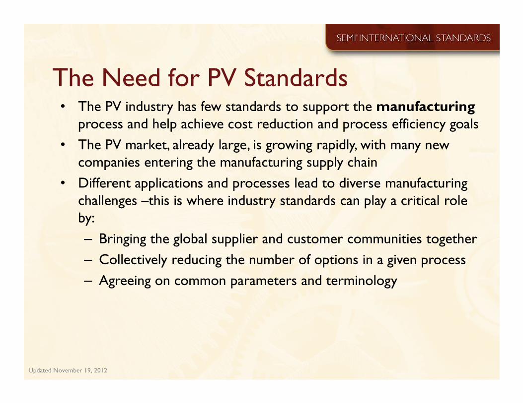
The Need for PV Standards• The PV industry has few standards to support the manufacturing
process and help achieve cost reduction and process efficiency goals
• The PV market, already large, is growing rapidly, with many new
companies entering the manufacturing supply chain
• Different applications and processes lead to diverse manufacturing
challenges –this is where industry standards can play a critical role
by:
– Bringing the global supplier and customer communities together
– Collectively reducing the number of options in a given process
– Agreeing on common parameters and terminology

Updated November 19, 2012
Outline
• Why PV Standards?
• Why SEMI?
• Global SEMI PV Standards Organization and Charters
• Regional Updates
• Background Information

Updated November 19, 2012
Why SEMI?• Similarity between semiconductor, FPD and PV manufacturing – many SEMI Standards immediately applicable
• Well-established (35+years), transparent process for developing international consensus manufacturing Standards
• Global infrastructure serving major PV manufacturing regions
• Over 500 volunteer experts working in SEMI PV Standards Activities, led by PV industry veterans

Updated November 19, 2012
PV Standards Developing Organizations

Updated November 19, 2012
Outline
• Why PV Standards?
• Why SEMI?
• Global SEMI PV Standards Organization and Charters
• Regional Updates
• Background Information

Updated November 19, 2012
Notable Companies Involved in Developing SEMI PV Standards
acp-IT AG
Air Liquide
Air Products
AIS Automation Dresden GmbH
AIST
Applied Materials
Asahi/America, Inc.
ATMI
Bosch Solar Energy AG
BP Solar
Brewer Science
CA Solar
Canon ANELVA Corporation
CH2M Hill
China Sunergy
Chroma ATE INC
Cimetrix
Corning
Covalent Materials Corporation
Daihen Corporation
Dainichi Shoji K.K.
DAINIPPON
Delsolar
Despatch Industries
Deutsche Solar AG
Dow Corning
DuPont
Entegris, Inc.
Evans Analytical Group
Ever Energy Co. Ltd.
Evergreen Engineering
First Solar
Fraunhofer
Freiberg
GCL
George Fischer
GT Solar
Hemlock Semiconductor
Hirata Corporation
Hitachi Kokusai Electric Inc.
Hynix Semiconductor Inc.
ICL Performance Products LLC
IMEC
ITRI
Japan Solar Silicon
Jonas&Redmann Automation
KANEKA CORPORATION
KLA-Tencor
Korea Institute of Lighting Technology
LDK
LG. Display
Linde LLC
M+W Zander FE GmbH
Manz Automation AG
Matheson Tri-Gas
MEMC Electronic Materials, Inc.
Meyer Burger
Mitsubishi Heavy Industries,LTD
Motech (Solar Division)
Nippon Steel Corp.
Nisshinbo Mechatronics Inc.
NIST
NREL
OC Oerlikon Balzers AG
OCI
Pall Corporation
Parker Hannifin
PEER Group GmbH
Q-Cells SE
REC Silicon
RENA GmbH
Renesola
Roth & Rau - Ortner GmbH
Schiller Automation
Schott Solar AG
Semilab
Sinton Instruments
Solar World
SUMCO
Sunicon AG
Suntech
Swagelok
Tokuyama corporation
Tokyo Electron Ltd.
Trina Solar
TUV
UL
ULVAC
Wacker Chemie AG
Updated November 19, 2012
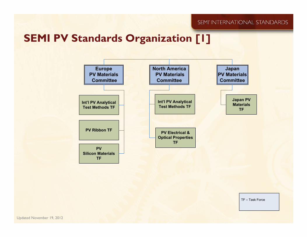
SEMI PV Standards Organization [1]
North America
PV Materials
Committee
Japan
PV Materials
Committee
Europe
PV Materials
Committee
PV Ribbon TF
Int’l PV Analytical
Test Methods TF
PV
Silicon Materials
TF
Int’l PV Analytical
Test Methods TF
PV Electrical &
Optical Properties
TF
Japan PV
Materials
TF
TF – Task Force
Updated November 19, 2012
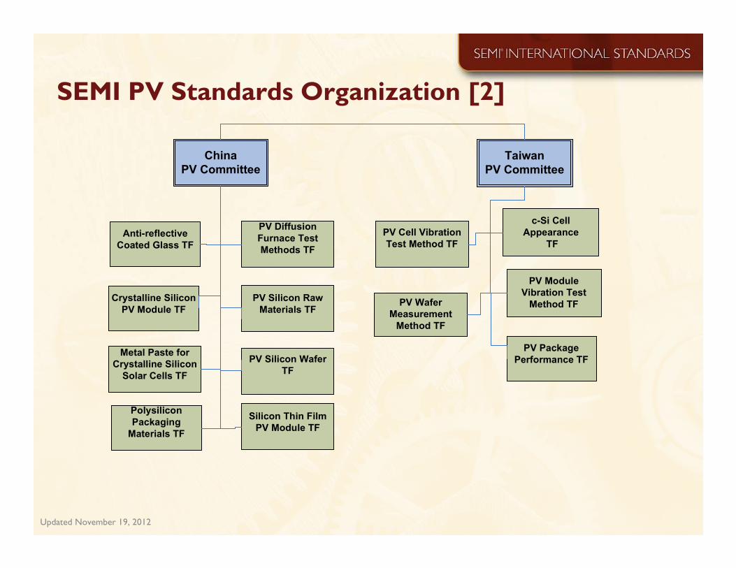
SEMI PV Standards Organization [2]
Taiwan
PV Committee
c-Si Cell
Appearance
TF
PV Module
Vibration Test
Method TFPV Wafer
Measurement
Method TF
PV Cell Vibration
Test Method TF
China
PV Committee
Polysilicon
Packaging
Materials TF
PV Diffusion
Furnace Test
Methods TF
PV Package
Performance TF
PV Silicon Raw
Materials TF
PV Silicon Wafer
TF
Silicon Thin Film
PV Module TF
Metal Paste for
Crystalline Silicon
Solar Cells TF
Anti-reflective
Coated Glass TF
Crystalline Silicon
PV Module TF

Updated November 19, 2012
SEMI PV Standards Organization [3]
Japan
PV Automation
Committee
Int’l PV Equipment
Interface Spec. TF
Europe
PV Automation
Committee
Int’l PV Equipment
Interface Spec. TF
Int’l PV Transport
Carrier TF
PV Wafer Traceability
TF
Int’l PV Transport
Carrier TF

Updated November 19, 2012
Global PV Standards Committee
• Formation approved July, 2007.
• Initial Committee in Europe. Committees also now formed in
China, Japan, NA, and Taiwan.
• Charter - Explore, evaluate, discuss, and create consensus-
based standard measurement methods, specifications,
guidelines, and practices that, through voluntary compliance,
will:
• promote mutual understanding and improved communication between users and suppliers of photovoltaic manufacturing equipment, materials and services, and
• enhance the manufacturing efficiency and capability so as to reduce manufacturing cost of the photovoltaic (PV) industry.
Updated November 19, 2012
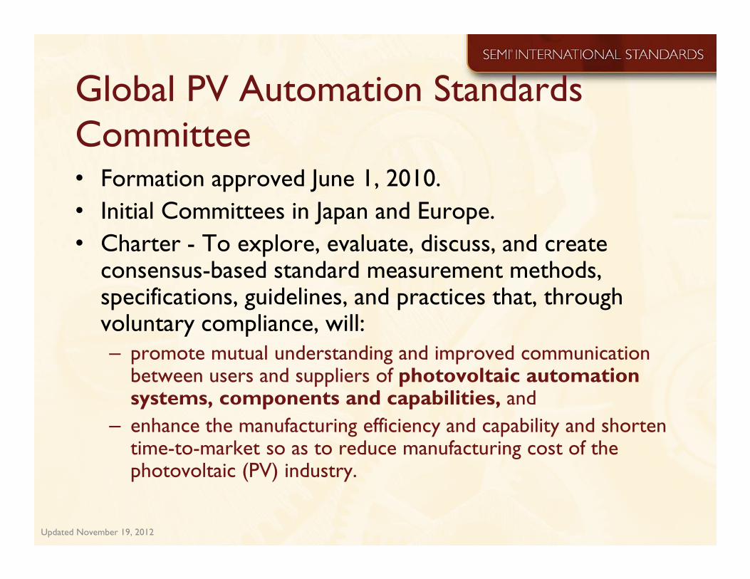
Global PV Automation Standards
Committee• Formation approved June 1, 2010.
• Initial Committees in Japan and Europe.
• Charter - To explore, evaluate, discuss, and create consensus-based standard measurement methods, specifications, guidelines, and practices that, through voluntary compliance, will:– promote mutual understanding and improved communication
between users and suppliers of photovoltaic automation systems, components and capabilities, and
– enhance the manufacturing efficiency and capability and shorten time-to-market so as to reduce manufacturing cost of the photovoltaic (PV) industry.
Updated November 19, 2012
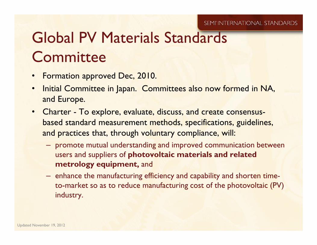
Global PV Materials Standards
Committee• Formation approved Dec, 2010.
• Initial Committee in Japan. Committees also now formed in NA,
and Europe.
• Charter - To explore, evaluate, discuss, and create consensus-
based standard measurement methods, specifications, guidelines,
and practices that, through voluntary compliance, will:
– promote mutual understanding and improved communication between users and suppliers of photovoltaic materials and related
metrology equipment, and
– enhance the manufacturing efficiency and capability and shorten time-to-market so as to reduce manufacturing cost of the photovoltaic (PV) industry.

Updated November 19, 2012
SEMI PV Standards [1]• PV1-0211 – Test Method for Measuring Trace Elements in Silicon
Feedstock for Silicon Solar Cells by High-Mass Resolution Glow Discharge Mass Spectrometry
– First standard test method that specifically addresses the evaluation of some types of PV Silicon feedstock.
• PV2-0709E – Guide for PV Equipment Communication Interfaces
– Unified communication standard between PV production equipment and the shop floor
• PV4-0311 – Specification for Range of 5th Generation Substrate Sizes for Thin Film Photovoltaic Applications
– Provides a range of substrate sizes for equipment applicable to 5th generation substrates
Updated November 19, 2012
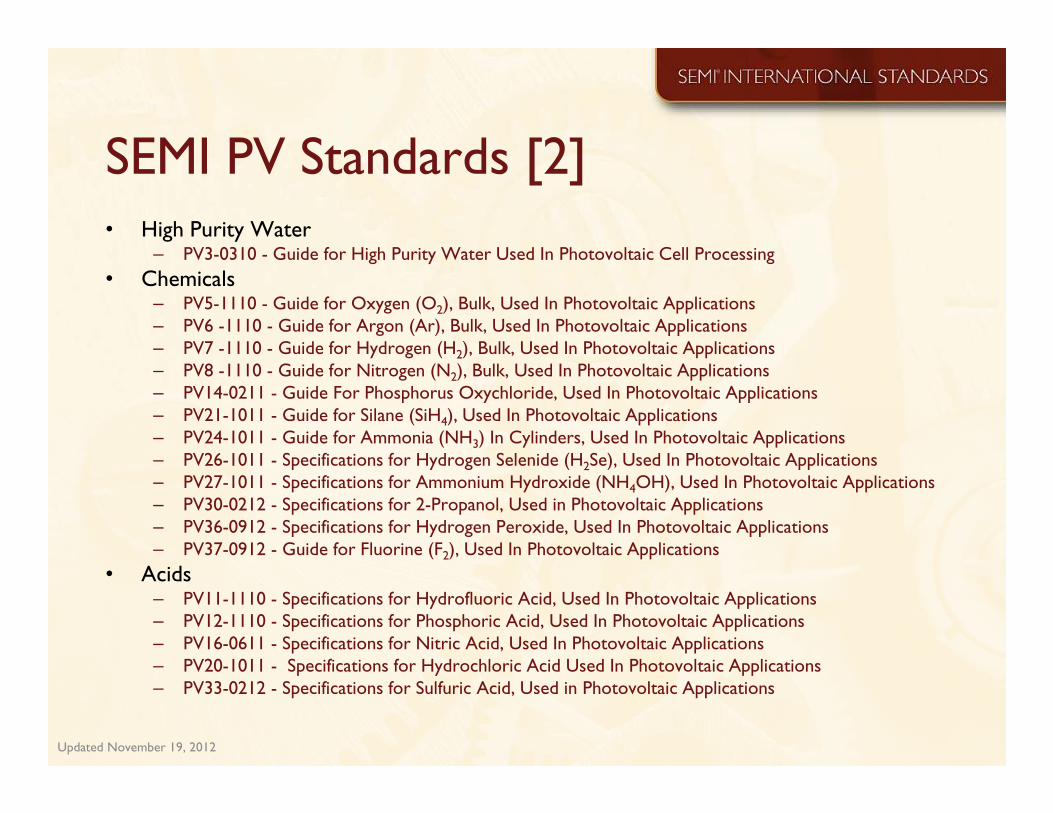
SEMI PV Standards [2]• High Purity Water
– PV3-0310 - Guide for High Purity Water Used In Photovoltaic Cell Processing
• Chemicals– PV5-1110 - Guide for Oxygen (O2), Bulk, Used In Photovoltaic Applications– PV6 -1110 - Guide for Argon (Ar), Bulk, Used In Photovoltaic Applications– PV7 -1110 - Guide for Hydrogen (H2), Bulk, Used In Photovoltaic Applications– PV8 -1110 - Guide for Nitrogen (N2), Bulk, Used In Photovoltaic Applications– PV14-0211 - Guide For Phosphorus Oxychloride, Used In Photovoltaic Applications– PV21-1011 - Guide for Silane (SiH4), Used In Photovoltaic Applications– PV24-1011 - Guide for Ammonia (NH3) In Cylinders, Used In Photovoltaic Applications– PV26-1011 - Specifications for Hydrogen Selenide (H2Se), Used In Photovoltaic Applications– PV27-1011 - Specifications for Ammonium Hydroxide (NH4OH), Used In Photovoltaic Applications– PV30-0212 - Specifications for 2-Propanol, Used in Photovoltaic Applications– PV36-0912 - Specifications for Hydrogen Peroxide, Used In Photovoltaic Applications– PV37-0912 - Guide for Fluorine (F2), Used In Photovoltaic Applications
• Acids– PV11-1110 - Specifications for Hydrofluoric Acid, Used In Photovoltaic Applications– PV12-1110 - Specifications for Phosphoric Acid, Used In Photovoltaic Applications– PV16-0611 - Specifications for Nitric Acid, Used In Photovoltaic Applications– PV20-1011 - Specifications for Hydrochloric Acid Used In Photovoltaic Applications– PV33-0212 - Specifications for Sulfuric Acid, Used in Photovoltaic Applications
Updated November 19, 2012
SEMI PV Standards [3]
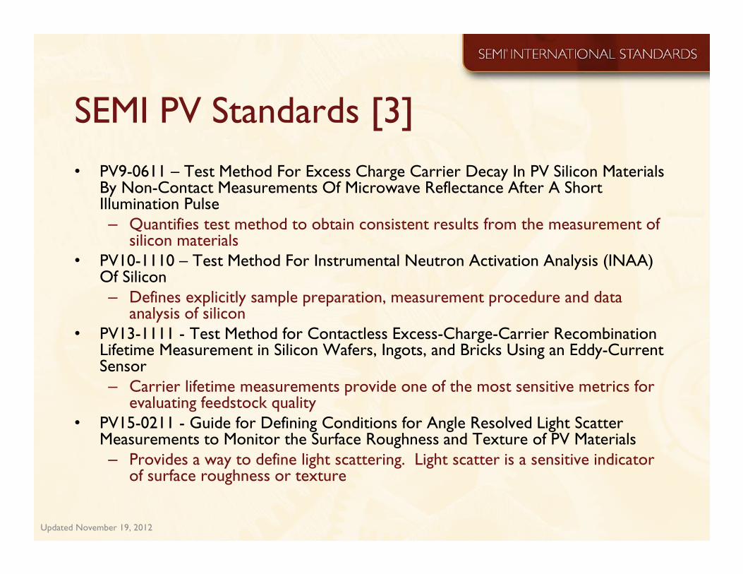
• PV9-0611 – Test Method For Excess Charge Carrier Decay In PV Silicon Materials By Non-Contact Measurements Of Microwave Reflectance After A Short Illumination Pulse
– Quantifies test method to obtain consistent results from the measurement of silicon materials
• PV10-1110 – Test Method For Instrumental Neutron Activation Analysis (INAA) Of Silicon
– Defines explicitly sample preparation, measurement procedure and data analysis of silicon
• PV13-1111 - Test Method for Contactless Excess-Charge-Carrier Recombination Lifetime Measurement in Silicon Wafers, Ingots, and Bricks Using an Eddy-Current Sensor
– Carrier lifetime measurements provide one of the most sensitive metrics for evaluating feedstock quality
• PV15-0211 - Guide for Defining Conditions for Angle Resolved Light Scatter Measurements to Monitor the Surface Roughness and Texture of PV Materials
– Provides a way to define light scattering. Light scatter is a sensitive indicator of surface roughness or texture
Updated November 19, 2012
SEMI PV Standards [4]
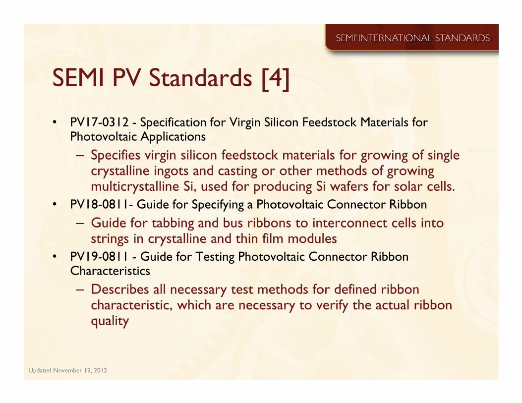
• PV17-0312 - Specification for Virgin Silicon Feedstock Materials for Photovoltaic Applications
– Specifies virgin silicon feedstock materials for growing of single crystalline ingots and casting or other methods of growing multicrystalline Si, used for producing Si wafers for solar cells.
• PV18-0811- Guide for Specifying a Photovoltaic Connector Ribbon
– Guide for tabbing and bus ribbons to interconnect cells into strings in crystalline and thin film modules
• PV19-0811 - Guide for Testing Photovoltaic Connector Ribbon Characteristics
– Describes all necessary test methods for defined ribbon characteristic, which are necessary to verify the actual ribbon quality
SEMI PV Standards [5]• PV22-1011- Specification for Silicon Wafers for Used in Photovoltaic Solar
Cells
– Requirements for silicon wafers for use in PV solar cell manufacture
• PV23-1011 - Test Method for Mechanical Vibration of Crystalline Silicon Photovoltaic (PV) Modules in Shipping Environment
– Evaluation of damaging to PV modules due to mechanical vibration during
transportation
• PV25-1011- Test Method for Simultaneously Measuring Oxygen, Carbon, Boron and Phosphorus in Solar Silicon Wafers and Feedstock by Secondary Ion Mass Spectrometry
– Measuring impurities in silicon by Second Ion Mass Spectrometry (SIMS)
• PV28-0212 - Test Methods for Measuring Resistivity or Sheet Resistance with a Single-Sided Noncontact Eddy-Current Gauge
– Measure resistivity in substrate used in PV devices using Eddy-Current
Updated November 19, 2012

SEMI PV Standards [6]
• PV29-0212 - Specification for Front Surface Marking of PV Silicon Wafers with Two-Dimensional Matrix Symbols
– Defines geometric and content of mark in 2-D code, machine-readable
• PV31-0212 - Test Method for Spectrally Resolved Reflective and Transmissive Haze of Transparent Conducting Oxide (TCO) Films for PV Application
– Measures haze in TCO film to characterize properties of material
• PV32-0312- Specification for Marking of PV Silicon Brick Face and PV Wafer Edge
– Defines brick slice code (BSC) mark for identifying and tracking wafers and bricks
• PV34-0712 - Practice for Assigning Identification Numbers to PV Si Wafer and Solar Cell Manufacturers
– Covers the assignment of identification numbers for crystalline PV Si wafer as well as
solar cell manufacturers and their locations.
Updated November 19, 2012

Updated November 19, 2012
SEMI PV Standards [7]
• PV35 - Specification for Horizontal Communication between Equipment for Photovoltaic Fabrication System
– Horizontal communication standard between PV equipment
• PV38 - Test Method for Mechanical Vibration of c-Si PV Cells in Shipping Environment
– Evaluation of damaging to PV cell due to mechanical vibration during transportation
• PV39 - Test Method for In-Line Measurement of Cracks in PV Silicon Wafers by Dark Field Infrared Imaging
– Inline measurement of crack on PV wafer
• PV40 - Test Method for In-Line Measurement of Saw Marks on PV Silicon Wafers by a Light Sectioning Technique Using Multiple Line Segments
– Inline measurement of saw mark on PV wafer
• PV41 - Test Method for In-Line, Non-Contact Measurement of Thickness and Thickness Variation of Silicon Wafers for PV Applications Using Capacitive Probes
– Inline measurement of thickness and thickness variation of PV wafer
Updated November 19, 2012
SEMI PV Auxiliary Information
• AUX017-0310E – Contactless Carrier-Lifetime Measurement in Silicon Wafer, Ingots, and Blocks
– Summary of a common framework for contactless carrier lifetime measurement in silicon photovoltaic
• AUX019-0211 – Interlaboratory Study Results For Determining the Precision of SEMI PV1
– Eight laboratories reports to establish precision for PV1
• AUX022-0611 - Conversion of Units For Impurity Concentrations In Silicon
– Converting concentration units (ppma, ppba or ppta) and absolute units (atoms/cm3)
• AUX024-0712 - List of PV and Semiconductor Shared Gases and Liquid Chemicals Standards
• AUX025-0712 - List of suppliers of Si bricks, Si Wafers and Photovoltaic c-SI Solar Cells for Use in the PV Industry
Updated November 19, 2012
Other SEMI Standards Applicable for
PV Manufacturing [1/2]• SEMI E10 - Specification for Definition and Measurement of Equipment
Reliability, Availability, and Maintainability (RAM)
• SEMI F47 - Specification for Semiconductor Processing Equipment Voltage Sag Immunity
• SEMI F108 - Guide for Integration of Liquid Chemical Piping Components for Semiconductor, Flat Panel Display, and Solar Cell Manufacturing Applications
• SEMI M6 - Specification for Silicon Wafers for Use as Photovoltaic Solar Cells
• SEMI M44 - Guide to Conversion Factors for Interstitial Oxygen in Silicon
• SEMI MF391 - Test Method for Minority Carrier Diffusion Length in Extrinsic Semiconductors by Measurement of Steady-State Surface Photovoltage
• SEMI MF1188 - Test Method for Interstitial Oxygen Content of Silicon by Infrared Absorption With Short Baseline
Updated November 19, 2012
Other SEMI Standards Applicable for
PV Manufacturing [2/2]• SEMI MF1619 - Test Method for Measurement of Interstitial Oxygen
Content of Silicon Wafers by Infrared Absorption Spectroscopy with p-Polarized Radiation Incident at the Brewster Angle
• SEMI MF1708 - Practice for Evaluation of Granular Polysilicon by Melter-Zoner Spectroscopies
• SEMI MF1727 - Practice for Detection of Oxidation Induced Defects in Polished Silicon Wafers
• SEMI MF1809 - Guide for Selection and Use of Etching Solutions to Delineate Structural Defects in Silicon
• SEMI MF1810 - Test Method for Counting Preferentially Etched or Decorated Surface Defects in Silicon Wafers
• SEMI S2 - Environmental, Health, and Safety Guideline for Semiconductor Manufacturing Equipment
• SEMI S26 - Environmental, Health, and Safety Guideline for FPD Manufacturing System

Updated November 19, 2012
Topics currently being worked on include
• Aluminum and silver pastes
• Analytical test methods
• Anti-reflective coated glass
• Cell appearance and defect detection
• Connector ribbon
• Equipment to equipment communication
• Minority carrier lifetime
• Process chemicals and gases
•Thin-film silicon module light soaking test method
• PV diffusion furnace test method
• PV wafer defect metrology
• PV wafer and cell transport carriers
• PV wafer mark and ID
• PV wafer and brick traceability
• Polysilicon and modules packaging
• Mono-like silicon wafer for PV cells
• Single substrate tracking
• Solar grade silicon feedstock
• Transparent conductive oxide
• Wafer defect in-line test methods
Updated November 19, 2012
Outline
• Why PV Standards?
• Why SEMI?
• Global SEMI PV Standards Organization and
Charters
• Regional Updates
• Background Information

Updated November 19, 2012
Europe PV Materials Standards Committee
• Co-Chairs
– Peter Wagner – Self
– Hubert Aulich – PV Crystalox Solar
• Task Forces
– PV Silicon Materials
– PV Ribbon
– PV Analytical Test Methods
EUROPE

Updated November 19, 2012
PV Silicon Materials TF [1/3]• Leader:
– Peter Wagner
– Several PV silicon producers are involved in the activity: Dow Corning, Elkem Solar, Hemlock, PV Crystalox Solar Silicon, Wacker Chemie, REC, Siliken and Sunicon.
• Charter: Develop and maintain standards regarding specifications for bulk silicon materials used in manufacturing solar cells.
– Identify missing standardized test methods for PV Silicon Materials
– Define and develop common understanding of terms used in PV industry
– Educate industry about new standards
– Develop new standardized test methods for PV Si Materials
EUROPE
Updated November 19, 2012
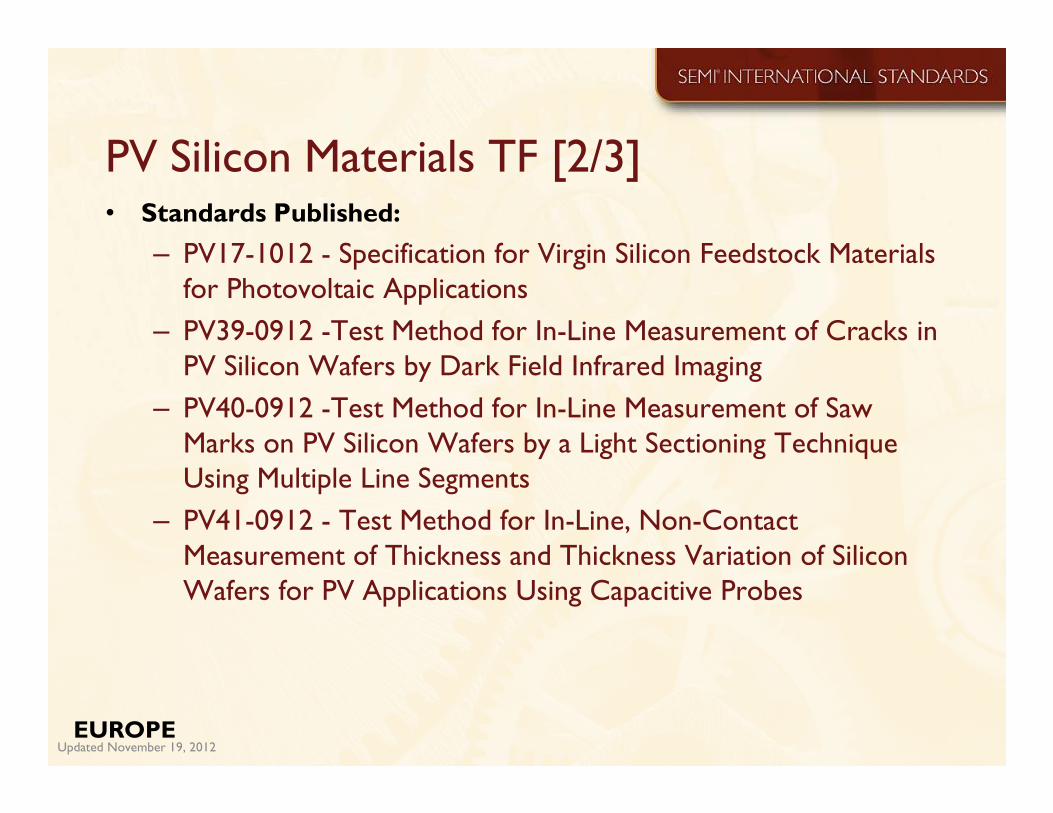
PV Silicon Materials TF [2/3]• Standards Published:
– PV17-1012 - Specification for Virgin Silicon Feedstock Materials
for Photovoltaic Applications
– PV39-0912 -Test Method for In-Line Measurement of Cracks in
PV Silicon Wafers by Dark Field Infrared Imaging
– PV40-0912 -Test Method for In-Line Measurement of Saw
Marks on PV Silicon Wafers by a Light Sectioning Technique
Using Multiple Line Segments
– PV41-0912 - Test Method for In-Line, Non-Contact
Measurement of Thickness and Thickness Variation of Silicon
Wafers for PV Applications Using Capacitive Probes
EUROPE

Updated November 19, 2012
PV Silicon Materials TF [3/3]
• New Activities:
– Ballot 5333, Test Method for In-Line Measurement of Waviness
on PV Silicon Wafers by a Light Sectioning Technique
• Approved by TC in October 2012, pending ISC A&R SC
review
– Doc. 5432, Test Method for In-Line Characterization of PV
Silicon Wafers by Using Photoluminescence
– Doc. 5433, Test Method for In-line Characterization of PV
Silicon Wafers Regarding Grain Size
– Doc. 5434, Test Method for In-Line Measurement of Lateral
Dimensions of PV Silicon Wafers for PV Applications
– Doc. 5530, Specification for Orientation Fiducials for PV Silicon
Wafers
EUROPE

Updated November 19, 2012
Other EU PV Materials Committee Task Forces• PV Ribbon TF
– Leader
• Christian Prischmann/Ulbrich
– Charter: Identify standardization needs for connector ribbon specifications and ribbon quality testing procedures
– Current Activities
• Guide for Specifying a Photovoltaic Connector Ribbon
– published as PV18-0912
• Guide for Testing Photovoltaic Connector Ribbon Characteristics
– published as PV19-0712
• Int’l PV Analytical Test Methods TF
– Refer to NA slides for latest update
EUROPE

Updated November 19, 2012
Europe PV Automation Committee
• Co-Chairs
– Eberhard Teichmann – Peer Group
• Task Forces
–PV Equipment Interface Specification (EIS)
–PV Transport Carrier
–PV Wafer Traceability
EUROPE

Updated November 19, 2012
PV Equipment Interface Specification
(EIS) Task Force [1/2]• Leader:
– C. Born/Viltronic
• Charter: Specify and define a unified equipment
communication interface for photovoltaic production
systems.
• Published
– SEMI PV2-0709E Guide for PV Equipment Communication
Interfaces, simplifying the application of the original SECS/GEM
(Semiconductor Equipment Communication Standards/Generic
Equipment Model)
EUROPE
Updated November 19, 2012
PV Equipment Interface Specification
(EIS) Task Force [2/2]
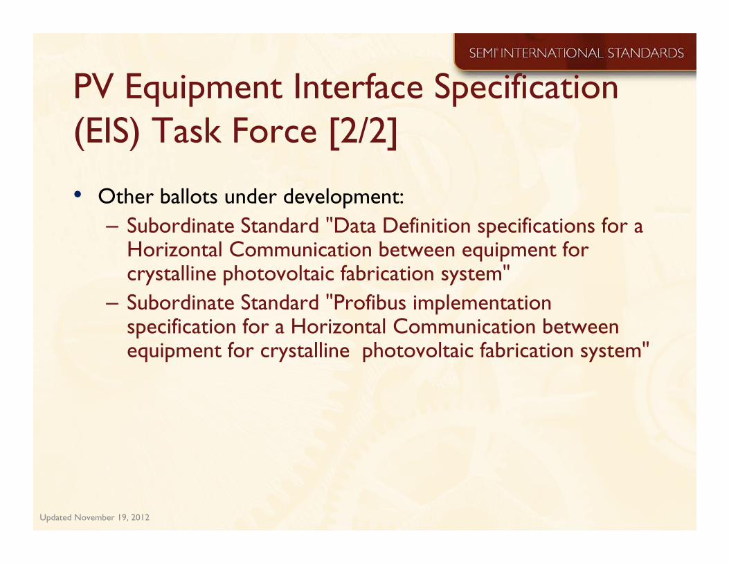
• Other ballots under development:
– Subordinate Standard "Data Definition specifications for a Horizontal Communication between equipment for crystalline photovoltaic fabrication system"
– Subordinate Standard "Profibus implementation specification for a Horizontal Communication between equipment for crystalline photovoltaic fabrication system"
Updated November 19, 2012
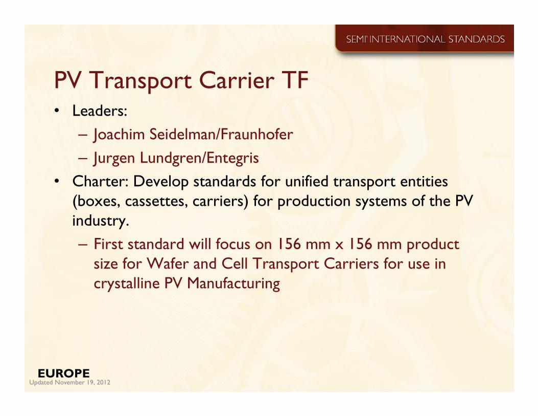
PV Transport Carrier TF • Leaders:
– Joachim Seidelman/Fraunhofer
– Jurgen Lundgren/Entegris
• Charter: Develop standards for unified transport entities
(boxes, cassettes, carriers) for production systems of the PV
industry.
– First standard will focus on 156 mm x 156 mm product
size for Wafer and Cell Transport Carriers for use in
crystalline PV Manufacturing
EUROPE

Updated November 19, 2012
PV Wafer Traceability TF [1/2]
• Leader
– Andreas Behr/Innolas Semiconductor
• Charter: Define standards for PV-wafer identification from the cut ingot (wafer) to the end of - and including - module production.
• Published
– PV29-0212 Specification for Front Surface Marking of PV Silicon Wafers with Two-Dimensional Matrix Symbols
– PV32-0312 Specification for Marking of PV Silicon Brick Face and PV Wafer Edge
– PV34-0712 Practice for Assigning Identification Numbers to PV Si Wafer and Solar Cell Manufacturers
EUROPE

Updated November 19, 2012
PV Wafer Traceability TF [2/2]
• Ballot under development– Ballot 5388 – Revision of PV34, Practice for Assigning Identification Numbers to PV Si Wafer and Solar Cell Manufacturers
• Approved by TC in October 2012, pending ISC A&R SC review
– Ballot 5418A - Revision of PV29, Specification for Front Surface Marking of PV Silicon Wafers with Two-Dimensional Matrix Symbols
• To be issued in cycle 1-2013 for review at PVFMF meeting
– Ballot 5151, Specification to Transfer Wafer Mark Reader Data To Host System (MES)
• Future work may include
– Investigation of anti-counterfeiting possibilities and PV recycling issues
EUROPE

Updated November 19, 2012
Crystalline Technology and
Manufacturing (CTM) Group• European group of eight crystalline solar cell manufacturers
(Q-Cells, Deutsche Cell, Bosch Solar Energy, Schott Solar, Sovello,
Sunways, SolarWatt and Solland) is working together within SEMI.
• The priority of the CTM Group will be the definition of the
development processes for raw materials, cell technology and cell
manufacturing.
• The CTM Group has established a crystalline solar cell technology
roadmap up to the year 2020
– www.itrpv.net
EUROPE
Updated November 19, 2012
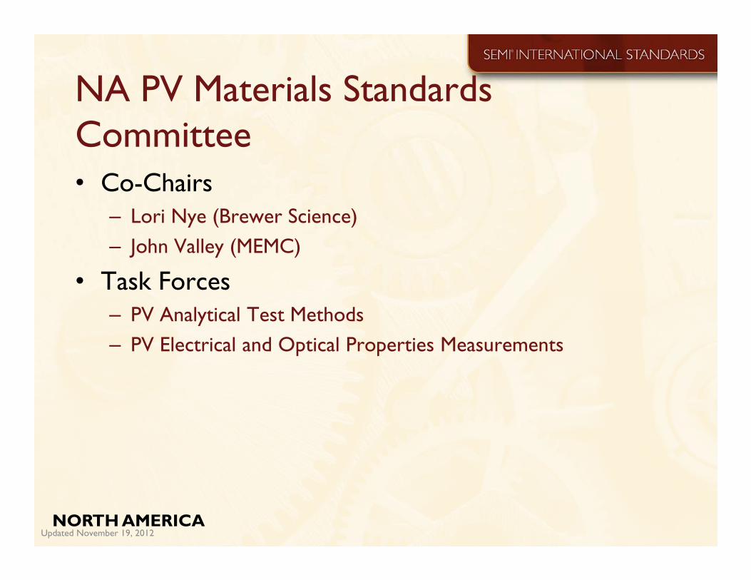
NA PV Materials Standards
Committee• Co-Chairs
– Lori Nye (Brewer Science)
– John Valley (MEMC)
• Task Forces– PV Analytical Test Methods
– PV Electrical and Optical Properties Measurements
NORTH AMERICA

Updated November 19, 2012
PV Analytical Test Methods TF [1]• Leader
– Hugh Gotts/Balazs Analytical Services
• Charter: develop standard analytical test methods for PV industry– Standards published
• PV1-0211, Test Method for Measuring Trace Elements in Silicon Feedstock for Silicon Solar Cells by High-Mass Resolution Glow Discharge Mass Spectrometry
• PV9-0611, Test Method for Excess Charge Carrier Decay in PV Silicon Materials by Non-Contact Measurements of Microwave Reflectance After a Short Illumination Pulse
• PV10-1110, Test Method For Instrumental Neutron Activation Analysis (INAA) Of Silicon
• PV13-1111, Test Method for Contactless Excess-Charge-Carrier Recombination Lifetime Measurement in Silicon Wafers, Ingots, and Bricks Using an Eddy-Current Sensor
• PV25-1011, Test Method for Simultaneously Measuring Oxygen, Carbon, Boron and Phosphorus in Solar Silicon Wafers and Feedstock by Secondary Ion Mass Spectrometry
•
NORTH AMERICA

Updated November 19, 2012
PV Analytical Test Methods TF [2]
• Published Auxiliary Information
– AUX017-0310, Contactless Measurement of Carrier Recombination Lifetime in Silicon
Wafers and Ingots
– AUX019-0211, Interlaboratory Study Results for Determining the Precision of PV1
– AUX022-0611, Conversion of Units for Impurity Concentrations in Silicon
• Drafting:
– Ballot 4675C, Test Method for Inductively-Coupled-Plasma Mass Spectrometry (ICP-MS) in Silicon Feedstock
• To be issued for Cycle 1-13 for review at NA Spring 2013
– Ballot 5438, Test Method for the Measurement of Oxygen Concentration in PV Silicon Materials by Inert Gas Fusion Infrared Detection Method
• Approved by TC in October 2012, pending ISC A&R SC review
NORTH AMERICA

Updated November 19, 2012
PV Analytical Test Methods TF [3]
• Drafting Auxiliary Information:
– Round Robin Report (Multi-laboratory Test) of SEMI PV9-1110, Test Method for Excess Charge Carrier Decay in PV Silicon Materials by Non-Contact Measurement of Microwave Reflectance After a Short Illumination Pulse
– Round Robin Report (Multi-laboratory Test) of SEMI PV25-1011, Test Method for Simultaneously Measuring Oxygen, Carbon, Boron and Phosphorus in Solar Silicon Wafers and Feedstock by Secondary Ion Mass Spectrometry
– Round Robin Report (Multi-laboratory Test) of doc. 5438, Test Method for the Measurement of Oxygen Concentration in PV Silicon Materials for Silicon Solar Cells by Inert Gas Fusion Infrared Detection Method
NORTH AMERICA

Updated November 19, 2012
PV Electrical and Optical Properties Measurements TF
• Leaders
– Chris Moore/Semilab and Austin Blew/LEI
• Charter: To develop standards or practices for non-destructive electrical properties measurements for the PV industry.
– Standards Published
• SEMI PV15-0211 - Guide for Defining Conditions for Angle Resolved Light Scatter Measurements to Monitor the Surface Roughness and Texture of PV Materials
• SEMI PV28-0212 - Test Methods for Measuring Resistivity or Sheet Resistance with a Single-Sided Noncontact Eddy-Current Gauge
• SEMI PV31-0212 - Test Method for Spectrally Resolved Reflective and Transmissive Haze of Transparent Conducting Oxide (TCO) Films for PV Application
• Drafting
– Doc. 4825, New standard: Test Methods for Hg Probe Measurements of Crystalline Silicon PV Materials and Devices
– Doc. 5394, New Standard: Test Method for QSS Microwave PCD measurements of Carrier Decay and Lifetime
NORTH AMERICA

Updated November 19, 2012
PV Materials Committee
– Published PV22-1011, Specification for Silicon Wafers for Use as Photovoltaic Solar Cells
• Withdrawal of SEMI M6-1108 Specification for Silicon Wafers for Use as Photovoltaic Solar Cells, was approved by Silicon Wafer Committee
NORTH AMERICA
Updated November 19, 2012
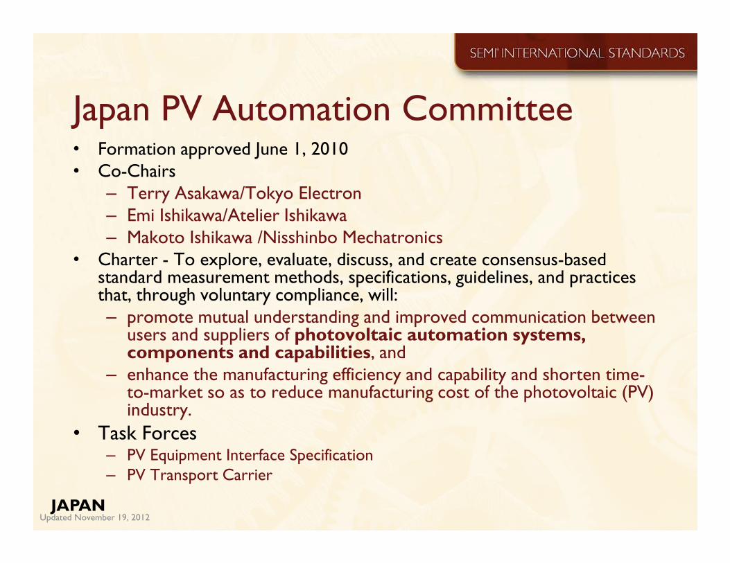
Japan PV Automation Committee• Formation approved June 1, 2010• Co-Chairs
– Terry Asakawa/Tokyo Electron– Emi Ishikawa/Atelier Ishikawa– Makoto Ishikawa /Nisshinbo Mechatronics
• Charter - To explore, evaluate, discuss, and create consensus-based standard measurement methods, specifications, guidelines, and practices that, through voluntary compliance, will:– promote mutual understanding and improved communication between
users and suppliers of photovoltaic automation systems, components and capabilities, and
– enhance the manufacturing efficiency and capability and shorten time-to-market so as to reduce manufacturing cost of the photovoltaic (PV) industry.
• Task Forces– PV Equipment Interface Specification
– PV Transport Carrier
JAPAN
Updated November 19, 2012
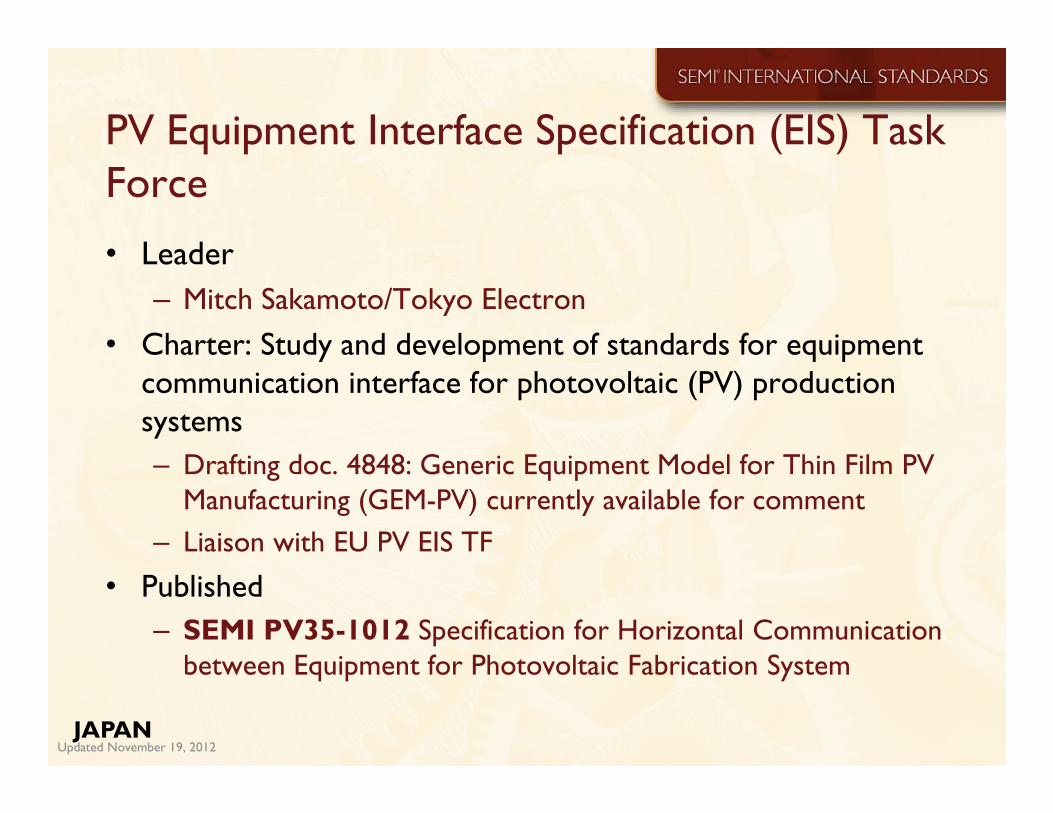
PV Equipment Interface Specification (EIS) Task
Force
• Leader
– Mitch Sakamoto/Tokyo Electron
• Charter: Study and development of standards for equipment
communication interface for photovoltaic (PV) production
systems
– Drafting doc. 4848: Generic Equipment Model for Thin Film PV
Manufacturing (GEM-PV) currently available for comment
– Liaison with EU PV EIS TF
• Published
– SEMI PV35-1012 Specification for Horizontal Communication
between Equipment for Photovoltaic Fabrication System
JAPAN
Updated November 19, 2012
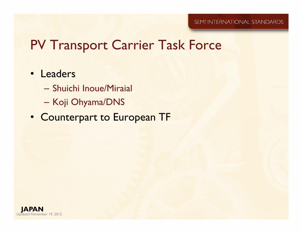
PV Transport Carrier Task Force
• Leaders
– Shuichi Inoue/Miraial
– Koji Ohyama/DNS
• Counterpart to European TF
JAPAN

Updated November 19, 2012
Japan PV Materials Committee
• Co-Chairs
– Takashi Ishihara/Mitsubishi Electric
– Kazuhiko Kashima/Covalent Materials
– Tetsuo Fukuda/Advanced Industrial Science and Technology
• Task Force
– PV Materials
JAPAN
Updated November 19, 2012
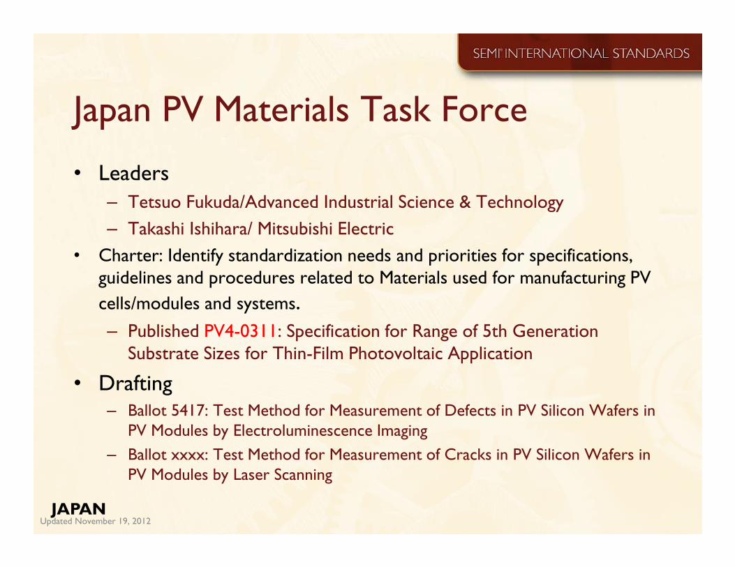
Japan PV Materials Task Force
• Leaders
– Tetsuo Fukuda/Advanced Industrial Science & Technology
– Takashi Ishihara/ Mitsubishi Electric
• Charter: Identify standardization needs and priorities for specifications, guidelines and procedures related to Materials used for manufacturing PV
cells/modules and systems.
– Published PV4-0311: Specification for Range of 5th Generation Substrate Sizes for Thin-Film Photovoltaic Application
• Drafting– Ballot 5417: Test Method for Measurement of Defects in PV Silicon Wafers in
PV Modules by Electroluminescence Imaging
– Ballot xxxx: Test Method for Measurement of Cracks in PV Silicon Wafers in
PV Modules by Laser Scanning
JAPAN
Updated November 19, 2012
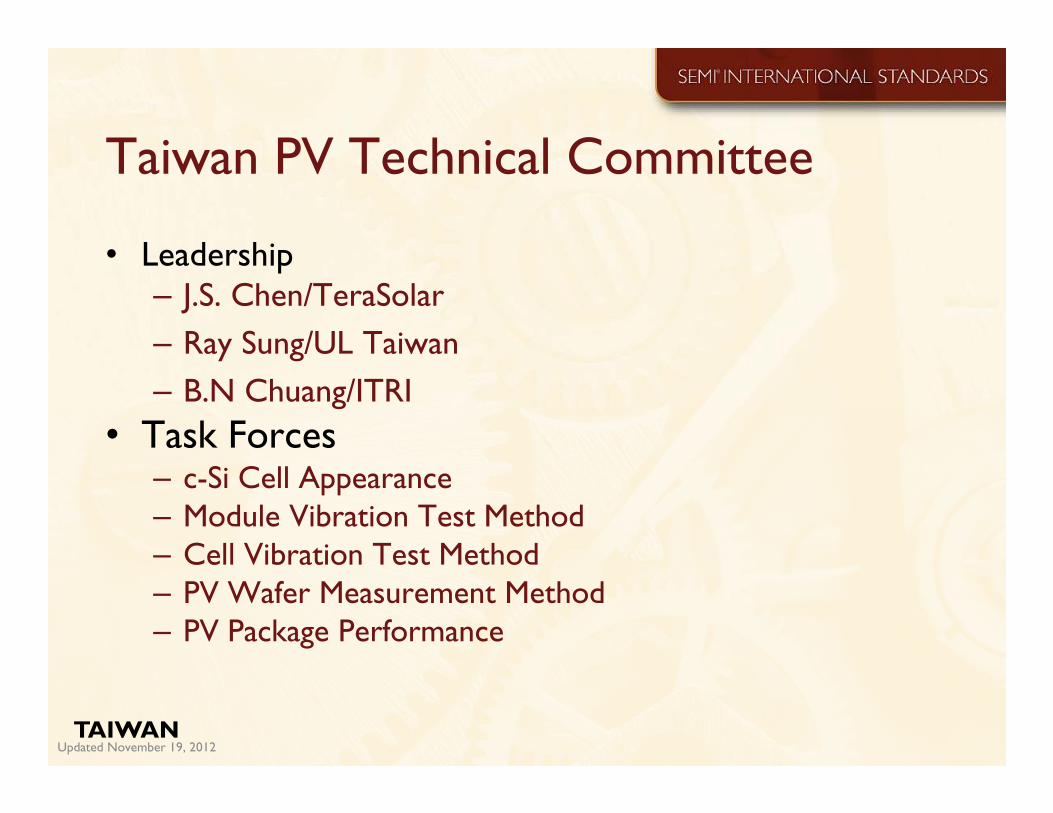
Taiwan PV Technical Committee
• Leadership– J.S. Chen/TeraSolar
– Ray Sung/UL Taiwan
– B.N Chuang/ITRI
• Task Forces– c-Si Cell Appearance
– Module Vibration Test Method
– Cell Vibration Test Method
– PV Wafer Measurement Method
– PV Package Performance
TAIWAN

Updated November 19, 2012
c-Si Cell Appearance TF
• Leader
– Jeff Lee/Chroma
• Charter: Due to increasing demand for quality, c-Si solar cell appearance characteristics such as chipped cell, stain on cell surface, cell color etc., have become standard test requirements for c-Si solar cell manufacturing. However, no standard has been set in this field. As a result, c-Si solar cell manufacturers may receive very different specs from different customers, which dramatically increases the cost and add loading in process control. This standard aims to gather industry consensus and provide a qualification and/or classification criteria for c-Si cell appearance.
– Drafting a Specification for Color reference cell and Detection of c-Si PV cell surface visible defects
TAIWAN
Updated November 19, 2012
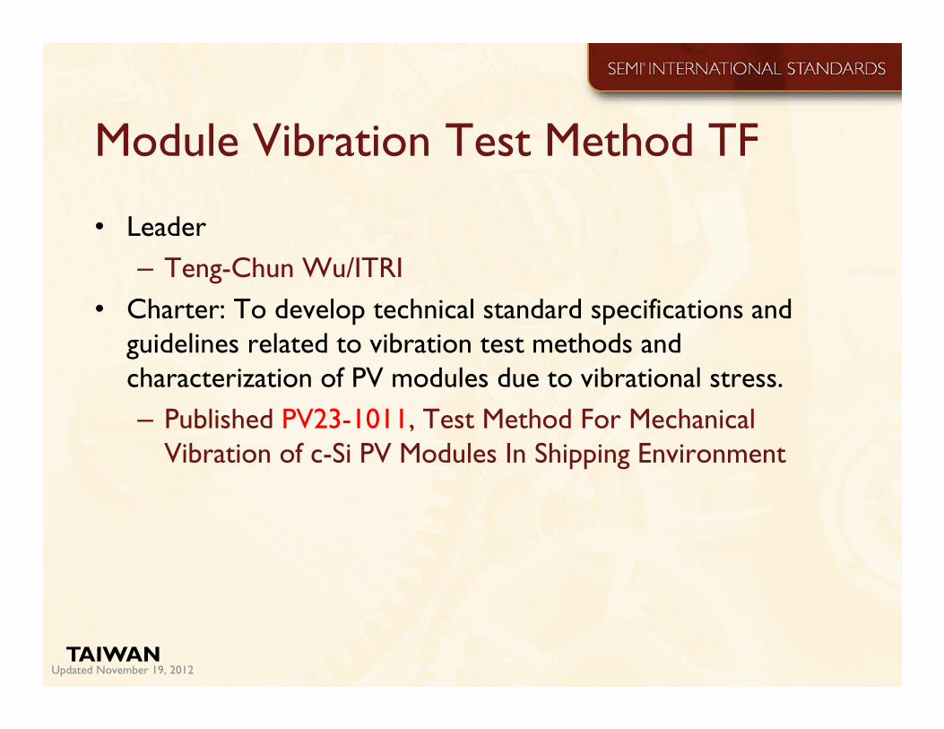
Module Vibration Test Method TF
• Leader
– Teng-Chun Wu/ITRI
• Charter: To develop technical standard specifications and
guidelines related to vibration test methods and
characterization of PV modules due to vibrational stress.
– Published PV23-1011, Test Method For Mechanical
Vibration of c-Si PV Modules In Shipping Environment
TAIWAN

Updated November 19, 2012
Cell Vibration Test Method TF
• Leader
– Teng-Chun Wu/ITRI
• Charter: The objective is to develop technical standard specifications and guidelines related to vibration test methods and characterization of PV cells due to the stress during shipping.
– Published PV35-0912 Test Method for Mechanical
Vibration of c-Si PV Cells in Shipping Environment
TAIWAN

Updated November 19, 2012
PV Wafer Measurement Method TF
• Leader– J.C Lin/Chunson
• Charter: Due to increasing demand for quality, PV Si Wafer
Metrology such as Geometry (Dimensions, TTV, Warp/Sori)
Electrical Character (Resistivity, Carrier Lifetime), Visible and
Non-Visible Defect, Saw-Mark, Stain on Wafer Surface, etc.,
have become standard test requirements for c-Si (both
Mono- and Multi- ) wafer manufacturing. However, no
standard has been set in this field.
TAIWAN

PV Package Performance TF
• Leader
– Teng-Chun Wu/ITRI
• Charter: The objective is to develop technical standard criteria related to PV wafer, cell and module package performance.
• Drafting:
– Ballot 5431: Test Method for Performance Criteria of
Photovoltaic (PV) Wafer, Cell, and Module Package
TAIWANUpdated November 19, 2012

Updated November 19, 2012
China PV Technical Committee
• Formation of China SEMI PV Standards Committee approved December 8, 2011, at SEMICON/PV Japan.
• Leadership– Guangchun Zhang/Suntech and Jun Liu/CESI
• Task Forces– Anti-Reflective Coated Glass – Crystalline Silicon PV Module– Metal Paste for Crystalline Silicon Solar Cells– Polysilicon Packaging Materials– PV Diffusion Furnace Test Methods– PV Silicon Raw Materials– PV Silicon Wafer– Silicon Thin Film PV Module
CHINA

Updated November 19, 2012
Anti-reflective Coated Glass TF
• Leaders
– Yin Bing/Suntech
– Zhu Xiaogang/CPVT
• Charter: Identify standardization needs and priorities and
develop specifications, guides and test methods for Anti-
reflective coated glass used in the manufacturing of crystalline
silicon solar modules.
• Drafting:
– Ballot 5475: Specification for Anti-Reflective Coated Glass, Used in Crystalline Silicon Photovoltaic Modules
CHINA
Updated November 19, 2012
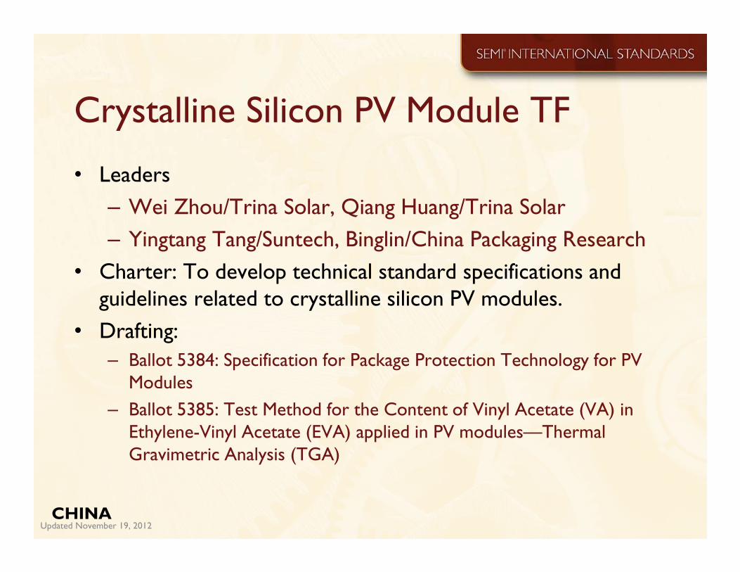
Crystalline Silicon PV Module TF
• Leaders
– Wei Zhou/Trina Solar, Qiang Huang/Trina Solar
– Yingtang Tang/Suntech, Binglin/China Packaging Research
• Charter: To develop technical standard specifications and
guidelines related to crystalline silicon PV modules.
• Drafting:
– Ballot 5384: Specification for Package Protection Technology for PV Modules
– Ballot 5385: Test Method for the Content of Vinyl Acetate (VA) in Ethylene-Vinyl Acetate (EVA) applied in PV modules—Thermal Gravimetric Analysis (TGA)
CHINA
Updated November 19, 2012
Metal Paste for Crystalline Silicon
Solar Cells TF• Leaders
– Chen Rulong/Suntech, Zhang Weiming/Heraeus
– Wang Mao/DuPont, Xu Shan/Rutech
• Charter: Identify standardization needs and priorities and
develop specifications, guides and test methods for metal
pastes used in the manufacturing of crystalline silicon solar
cells.
• Drafting:
– Ballot 5426: Specification for Aluminum Paste, Used in Back Surface Field of Crystalline Silicon Solar Cells
– Ballot 5427: Specification for Front Surface Silver Paste, Used in P-Type Crystalline Silicon Solar Cells
CHINA

Updated November 19, 2012
Polysilicon Packaging Materials TF
• Leaders
– Jinbiao Lv/GCL Poly
– Xiaoxia Liu/GCL
• Charter: Based on the input and feedback of polysilicon
manufacturers, develop standards for materials used for
packaging polysilicon.
• Drafting:
– Ballot 5428: Specification for Impurities in Polyethylene
Packaging Materials for Polysilicon Feedstock
CHINA
Updated November 19, 2012
PV Diffusion Furnace Test Methods TF
• Leaders
– Liu Liangyu/48th Institute
• Charter: Identify standardization needs and priorities and
develop test methods related to diffusion furnaces to help
evaluate the performance of heater tubes.
• Drafting:
– Ballot 5429: Test Method for In-line Monitoring of Flat
Temperature Zone in Horizontal Diffusion Furnaces
CHINA
Updated November 19, 2012
PV Silicon Raw Materials TF
• Leaders
– Dazhou Yan/SINOSICO and Li He/CPVT
• Charter: Identify standardization needs and priorities for
specifications, guides and test methods related to silicon raw
materials used for manufacturing solar-grade polysilicon.
• Drafting:
– Ballot 5476: Test Method for Determination Of Total Carbon Content in Silicon Powder by Infrared Absorption After Combustion in an Induction Furnace
– Ballot 5477: Test Method for Determining B, P, Fe, Al, Ca Contents in Silicon Powder for PV Applications by Inductively-Coupled-Plasma Optical Emission Spectrometry
CHINA
Updated November 19, 2012
PV Silicon Wafer TF
• Leaders
– Yuepeng Wan/LDK, Xiaoyong Wang/JAsolar
– Jingang Lu/Suntech,
• Charter: Identify standardization needs and priorities for
specifications, guidelines and procedures related to silicon
wafer used for manufacturing PV cells. Develop standards for
measuring electrical, physical and optical properties of silicon
wafer used for manufacturing PV cells.
• Drafting:
– Ballot 5382: Specification for Mono-Like Silicon Wafer for Use in Photovoltaic Solar Cells
CHINA

Updated November 19, 2012
Silicon Thin Film PV Module TF
• Leaders
– Mai Yaohua/Baoding Tianwei Solarfilms
– Niu Xinwei/Chint Solar
– Wu Zhenyu/Hanergy
• Charter: To develop new standardized test methods,
technical specifications and guides for thin film silicon PV
modules.
• Drafting:
– Ballot 5478: Test method for thin-film silicon PV modules
light soaking
CHINA
Participating Companies
• Increasing participation
from major Chinese PV
companies
Industry Segment Company Name
Wafer/C-Si Cell/Module Suntech
Wafer/C-Si Cell/Module JA Solar
Poly/Wafer/C-Si
Cell/ModuleYingli
Wafer/C-Si Cell/Module Trina
C-Si Cell/Module/TF Astronergy
Poly/Wafer/C-Si
Cell/ModuleLDK
Poly/Wafer/Installation GCL
Poly/Wafer Sinosico
Equipment/C-Si
Cell/ModuleCETC-48
Equipment Sevenstar
Standardization Institute CESI
Equipment Jingyuntong
C-Si Cell/Module Canadian Solar
PVApplication ERI of NDRC
Updated November 19, 2012
CHINA

Updated November 19, 2012
Korea
• PV Standards WG in the process of forming– Industry open forum in 2010
• Participating segments included: equipment, polysilicon, wafer-based cell/module
– Next steps
• Additional polysilicon suppliers invited for next meeting
• Once consensus on standards activities is reached, a PV Standards WG will be formed
– Target 4th quarter of 2012
KOREA
Updated November 19, 2012
Next PV Standards Committee and Task Force Meetings 2012 & 2013• Japan
– PV Japan, December 5-7, 2012
• Taiwan
– SEMI Taiwan office, December 21, 2012
• Europe
– PV Fab Managers Forum, Berlin, March 12-13, 2013
• China
– Solarcon China, Shangai, March 18, 2013
• NA
– Spring Standards Meetings, San Jose, CA, April 2-3, 2013
• www.semi.org/standards (calendar of events)

Updated November 19, 2012
International PV Module Quality
Assurance Forum• Environment-Specific Module Durability Testing
• July 15-16, 2011, San Francisco, CA, USA (Completed)
• Hosted By NREL and AIST, supported by SEMI PV Group.
• There are currently no standards that quickly assess a module’s ability to withstand regional stresses or a module’s durability over decades of use.
• A rating system that provides comparative information about the durability of PV modules against a variety of stresses will be a useful tool to PV consumers and provide a starting point for improving the accuracy of quantitative PV lifetime predictions.
• Proceedings at
– http://www.nrel.gov/ce/ipvmqa_forum/proceedings.cfm

Updated November 19, 2012
International PV Module Quality
Assurance Forum
• A standard PV module rating system would be valuable for:
– Incentive programs: define a minimum durability for module designs
– Investors: reduce interest rates for modules meeting a minimum criterion
– Insurance companies: reduce rates for modules meeting a minimum criterion
– Community: reduce installed PV cost by providing durability standards that lead to the desired durability without adding unnecessary cost
– PV module suppliers: optimize module design to minimize cost and secure desired reliability for specific market/customer
– PV module materials suppliers: reduce cost of materials by better communication with customers.
Updated November 19, 2012
For more information:
• www.pvgroup.org/standards
• www.semi.org/standards

Updated November 19, 2012
Contact Information• PV Standards – General
– James Amano ([email protected])
• PV Standards – Europe
– Yann Guillou ([email protected])
• PV Standards – North America
– Kevin Nguyen ([email protected])
• PV Standards – Japan
– Hiro’fumi Kanno ([email protected])
• PV Standards – China
– Kris Shen ([email protected])
• PV Standards – Taiwan
– Catherine Chang ([email protected])
• PV Standards – Korea
– Natalie Shim ([email protected])
• PV Standards – India
– Vijay Kundaji ([email protected])
Updated November 19, 2012
Outline
• Why PV Standards?
• Why SEMI/PV Group?
• Global SEMI PV Committee Organization and
Charter
• Regional Updates
• Background Information

Updated November 19, 2012
SEMI : The Global Association
• SEMI products and services include:• Expositions: SEMICON®, FPD, PV• International Standards
• Market research & statistics• Public policy/EHS• Technical & Business Conferences • Website: semi.org
SEMI is the industry association serving the
manufacturing supply chains for the
microelectronic, display and photovoltaic
industries.
HsinchuHsinchu
SeoulSeoul TokyoTokyo
SingaporeSingapore
BeijingBeijing
San JoseSan Jose BrusselsBrussels
MoscowMoscow
Washington DCWashington DC
ShanghaiShanghai HsinchuHsinchu
BerlinBerlin
BangaloreBangalore

Updated November 19, 2012
About PV Group
•SEMI members actively involved in PV manufacturing form the PV Group to address opportunities and obstacles to bringing low-cost PV technology and sustainable clean energy to the world.
Updated November 19, 2012
Why Standards?
• Define interfaces (hardware and software)
• Clearly characterize materials
• Improve supply chain communication
• Optimize environment, health and safety for the operators and others in the industry
• Results
– Cost reduction
– Focus on product differentiation
– Acceleration of product development
– Accepted verification procedures (test methods)
Updated November 19, 2012
Economic Impact of Standards• US National Institute of Standards and Technology (NIST)
Study
– Calibration, Standard Test Methods, and Software Standards
• $9.6 billion in benefits between 1996 and 2011
• Association Française de Normalisation (AFNOR) Study
– Over 70% of companies participating in standardization reported that it enabled them to anticipate future market requirements
• German Industry Study (DIN)
– Standards contribute more to economic growth than patents and licenses
• UK Department of Trade and Industry
– Standards contribute £2.5 billion annually to economic growth in the UK
Updated November 19, 2012
SEMI International Standards
Program History• Key Topics
– 1973• Silicon Wafers
– Late 1970’s• Chemicals and Gases• Metrology• Facilities
– Late 1980’s• Factory Automation
– Early 1990’s• Safety Guidelines
– 1994• 300mm
– 2007• Photovoltaics
– 2008• 450mm
– 2011• HB LED and 3DS-IC
• New Regions– 1973
• United States
– 1980’s
• Japan
• Europe
– 1990’s
• Taiwan
• Korea
– 2010
• China
Updated November 19, 2012
Document Development Path
• Technology Trends
• Suppliers
• Users
• Other Stakeholders
INDUSTRY NEEDS
Use
Ballot
Submission
Ballot Distribution
Approval
Draft
(Task Force)
Idea to
Committee
Ballot
Voting /Tallying
Publishing
Ballot
Adjudication
Procedural
Review

Updated November 19, 2012
The SEMI Standards Program Today
• All aspects of an automated fab are addressed
• Over 4000 volunteer experts
– 23 global technical committees
– 200 task forces
• Currently over 800 SEMI Standards and Safety Guidelines available
Updated November 19, 2012
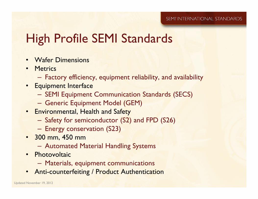
High Profile SEMI Standards
• Wafer Dimensions
• Metrics
– Factory efficiency, equipment reliability, and availability
• Equipment Interface
– SEMI Equipment Communication Standards (SECS)
– Generic Equipment Model (GEM)
• Environmental, Health and Safety
– Safety for semiconductor (S2) and FPD (S26)
– Energy conservation (S23)
• 300 mm, 450 mm
– Automated Material Handling Systems
• Photovoltaic
– Materials, equipment communications
• Anti-counterfeiting / Product Authentication

Updated November 19, 2012
Organizational Structure
SEMI Board of Directors Oversees the SEMI Standards Program
International Standards
Committee
Develops and maintains the SEMI Standard Regulations. Oversees
program coordination among geographical regions
Regional Standards
Committee
Provides continuing supervision of standards development in a
given geographical area
Technical Committees Provides the technical expertise in the standards process
Subcommittees Oversees task force activities and submits their reports to the
technical committee
Task Forces Develops and maintains most of the standards

Updated November 19, 2012
Get involved!
• Get your company support
• Register at http://www.semi.org/standards
– Sign up for Standards Watch Newsletter
• Establish ties with other regions’ Technical Committees and Task Forces
– Gather information on activities and trends
– Attend regional meetings
• Use SEMI Standards
– Benefit from cost reduction
– Download from SEMI Standards Web Site
– Purchase a SEMIViews license
Updated November 19, 2012
Chroma ATE INC
CI Industrial Safety Consulting, LLC
CiS Forschungsinstitut für Mikrosensorik und Photovoltaik GmbH
CMS/ITRI
Conexant Systems
Cook Engineering, Inc.
Covalent Materials Corporation
Daewon SPIC
Daihen Corporation
Dainichi Shoji K.K.
DAINIPPON
Delsolar
Despatch Industries
Deutsche Solar AG
Dow Corning
DuPont De Nemours International S.A.
DuPont Teijin Films
ECN Solar Energy
Energy Innovation Associates
ENspring
Entegris, Inc.
Evans Analytical Group
Ever Energy Co. Ltd.
Evergreen Engineering
Exponent Inc.
Fraunhofer
Freiberg
Fuji Electric Advanced Technology Co., Ltd.
GEASOL ltd
Gintech Energy Cooperation
Gnostic Systems
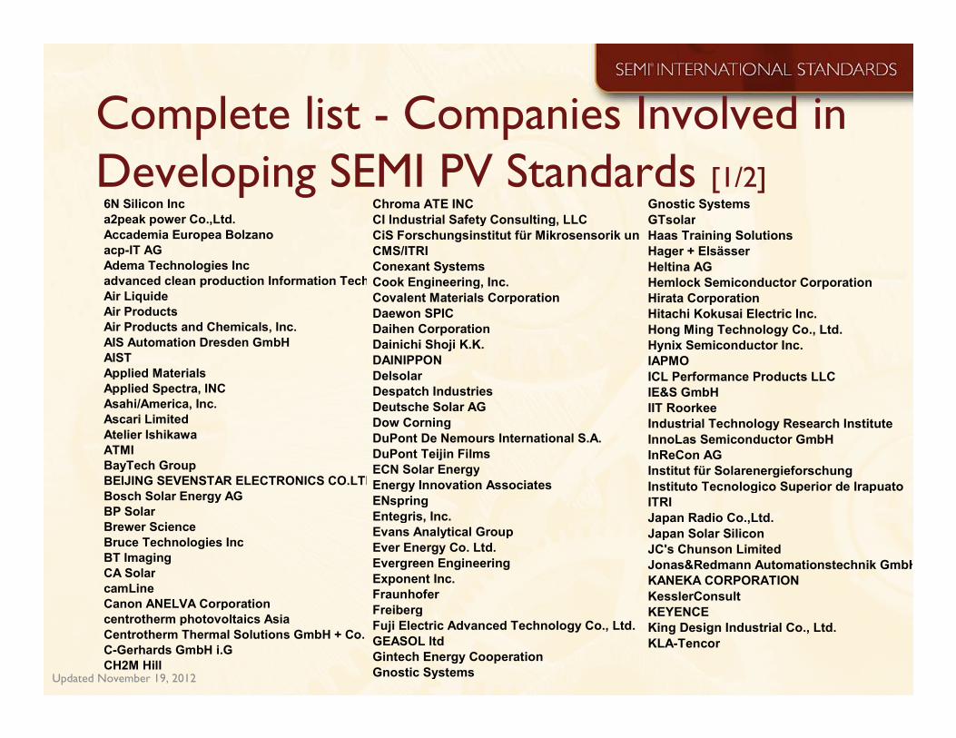
Complete list - Companies Involved in
Developing SEMI PV Standards [1/2]6N Silicon Inc
a2peak power Co.,Ltd.
Accademia Europea Bolzano
acp-IT AG
Adema Technologies Inc
advanced clean production Information Technology
Air Liquide
Air Products
Air Products and Chemicals, Inc.
AIS Automation Dresden GmbH
AIST
Applied Materials
Applied Spectra, INC
Asahi/America, Inc.
Ascari Limited
Atelier Ishikawa
ATMI
BayTech Group
BEIJING SEVENSTAR ELECTRONICS CO.LTD
Bosch Solar Energy AG
BP Solar
Brewer Science
Bruce Technologies Inc
BT Imaging
CA Solar
camLine
Canon ANELVA Corporation
centrotherm photovoltaics Asia
Centrotherm Thermal Solutions GmbH + Co. KG
C-Gerhards GmbH i.G
CH2M Hill
Gnostic Systems
GTsolar
Haas Training Solutions
Hager + Elsässer
Heltina AG
Hemlock Semiconductor Corporation
Hirata Corporation
Hitachi Kokusai Electric Inc.
Hong Ming Technology Co., Ltd.
Hynix Semiconductor Inc.
IAPMO
ICL Performance Products LLC
IE&S GmbH
IIT Roorkee
Industrial Technology Research Institute
InnoLas Semiconductor GmbH
InReCon AG
Institut für Solarenergieforschung
Instituto Tecnologico Superior de Irapuato
ITRI
Japan Radio Co.,Ltd.
Japan Solar Silicon
JC's Chunson Limited
Jonas&Redmann Automationstechnik GmbH
KANEKA CORPORATION
KesslerConsult
KEYENCE
King Design Industrial Co., Ltd.
KLA-Tencor

Updated November 19, 2012
Companies Involved in Developing
SEMI PV Standards [2/2]Korea Institute of Lighting Technology
Lanco Solar Pvt Ltd
Lewis Bass International Inc
LG Electronics, Inc.
LG. Display
Linde LLC
M+W Zander FE GmbH
Malema Engineering
Manz Automation AG
Materials & Metrology
Matheson Tri-Gas
MEMC Electronic Materials, Inc.
Meyer Burger AG
Micronit
Mitsubishi Electric Corporation
Mitsubishi Heavy Industries,LTD
Mitsuishi Bussan Corporation Limited
Mizuho Information & Research Institute, Inc.
MOSERBAER PHOTOVOLTAIC LIMITED
Motech (Solar Division)
Nippon Steel Corp.
Nisshinbo Mechatronics Inc.
NIST
Nokia Siemens Networks
NREL
NS Solar Material Co., Ltd.
NSN
OC Oerlikon Balzers AG
OCI
Omron
Op-tection GmbH
OptiSolar
Orient Service Corporation
Pall Corporation
Parker Hannifin
PEER Group GmbH
Polar Star Research, LLC
Prediktor AS
PVTC/ITRI
Q-Cells SE
QSES Inc.
R.A.Smythe, Management Consultants
RAPT Industries, Inc.
Raytex Corporation
REC Silicon
RENA GmbH
Roth & Rau - Ortner GmbH
RTS Corporation
Safe Techno Limited
Salmon Leap Associates India (p) Ltd
Salus
Schott Solar AG
Semilab
Semisol
SEMITRAC
Sentech Instruments GmbH
Sigma-Aldrich
Silicon Solar
Siliken Chemicals
SINTEF Materials and Chemistry
Sinton Instruments
SITEX 45 SRL
Sixtron Advanced Materials
Solar World
SolarTech
Solland Solar Cells GmbH
SPIL
SUMCO
Sunicon AG
Suntech Power Holdings Co., Ltd.
Swagelok
Tainergy Tech Co., Ltd
TAIYO NIPPON SANSO CORPORATION
The Scatter Works, Inc.
TNO Industrie en Techniek
Tokuyama corporation
Tokyo Electron Ltd.
Toray Research Center,Inc.
Tronic International Pte Ltd
TUV
ULVAC
Underwriters Laboratories Taiwan
UNI3 Ssytem Co., Ltd.
Universidad Carlos III de Madrid
University of Oxford
Voltaix. LLC
VQC
Wacker Chemie AG
Yaskawa Electric Corporation


