
Chemical Structure and Physical Properties of
Organic-Inorganic Metal Halide Materials for
Solid State Solar Cells
Majid Safdari
Doctoral Thesis
KTH Royal Institute of Technology
School of Chemical Science and Engineering
Department of Chemistry
Stockholm 11428, Sweden January 2017

Copy right © Majid Safdari
All rights reserved
TRITA-CHE- Report 2017:4
ISSN 1654-1081
ISBN 978-91-7729-233-3
Akademisk avhandling som med tillstånd av Kungliga Tekniska Högskolan i Stockholm
framlägges till offentlig granskning för avläggande av doktorsexamen i kemi fredagen
den 27 januari 2017 kl 13.30 i sal F3, KTH, Lindstedtsvägen 26, Stockholm.
Avhandlingen försvaras på engelska. Opponent är Dr. Timothy Kelly, University of
Saskatchewan, Kanada.

To my family

Abstract Methylammonium lead (II) iodide has recently attracted considerable
interest which may lead to substantial developments of efficient and
inexpensive industrial photovoltaics. The application of this material as
a light-absorbing layer in solid-state solar cells leads to impressive
efficiency of over 22% in laboratory devices. However, for industrial
applications, fundamental issues regarding their thermal and moisture
stability need to be addressed. MAPbI3 belongs to the perovskite family
of materials with the general formula ABX3 ,where is the organic cation
(methylammonium) which is reported to be a major source of
instability. In this work, a variety of alkyammonium lead (II) iodide
materials have been synthesized by changing the organic cation, to
study the relationship between the structural and physical properties of
these materials. Methylammonium, ethylammonium and
propylammonium were used for the [(A)PbI3] series. In another set of
experiments, butyldiammonium, hexyldiammonium, and
octyldiammonium cations were studied as (A)PbI4 perovskite materials.
Various dimensionalities for the structures of these materials were
found; three dimensional (3D) networks (MAPbI3, MAPbBr3), two
dimensional (2D) layered systems (BdAPbI4, HdAPbI4, OdAPbI4), and
one dimensional (1D) columns (EAPbI3, PAPbI3, EAPb2I6). Several new
lower dimensional materials (2D and 1D) were investigated and
reported for the first time. X-ray single crystallography was used to
obtain the detailed structures of the products. Bulk structures were
confirmed by comparison of the X-ray diffraction patterns with single
crystal data. [PbI6] octahedral structural units were repeated through the
material network depending on the dimensionality and connectivity of
the materials. Where a bulkier cation was introduced, the
crystallographic unit cell increased in size which resulted in lower
symmetry crystals. The connectivity of the unit cells along the material
networks was found to be based on corner-sharing and face-sharing.
Lower dimensionality resulted in larger bandgaps and lower
photoconductivity, and hence a lower light conversion efficiency for the
related solar cells. The thermal and moisture stability was greater in the
1D and 2D materials with bulkier organic cations than with

methylammonium. The electronic structure of the new 2D layered
perovskites was investigated by X-ray photoelectron spectroscopy, X-
ray absorption spectroscopy and X-ray emission spectroscopy. Density
functional theory was applied to calculate band structures, densities of
states and partial densities of states. These findings were in agreement
with the experimental part, indicating that the valence band is
composed mainly of iodine orbitals, while lead orbitals predominate in
the conduction band. The iodide/lead ratio obtained from surface
analysis of the material deposited on the TiO2 films matched the
proposed general formula from single crystal data.
In total, an overview is provided of the relationship between the
chemical dimensionality and physical properties of the organic-
inorganic lead halide materials with focus on the solar cell application.
Keywords: Perovskite, Solar cells, Organic-inorganic lead halide,
Dimensionality, Bandgap, X-ray diffraction, X-ray spectroscopy.

Svenska sammandrag:
Metylammoniumbly(II)jodid har under de senaste åren genererat ett
stort intresse som ett möjligt material for utveckling av effektiva och på
industriell skala billiga solceller. Detta material har använts som
ljusabsorberande skikt i fasta solceller med imponerande
omvandlingseffektiviteter på över 22% för solceller i laboratorieskala.
För att denna nya typ av solceller ska bli intressanta för produktion på
industriell skala, så behöver grundläggande frågeställningar kring
materialens stabilitet avseende högre temperaturer och fukt klargöras.
MAPbI3 har formellt perovskitstruktur med den allmänna formel ABX3,
där A utgörs av den organiska katjonen (metyammoniumjonen) och
som kan kopplas till materialets instabilitet. I denna avhandling har
olika alkylammoniumbly(II)jodidmaterial syntetiserats där den
organiska katjonen modifierats med syftet att studera växelverkan
mellan struktur och fysikaliska egenskaper hos de resulterande
materialen. Material av olika dimensionalitet erhölls; tredimensionella
(3D) nätverk (MAPbI3, MAPbBr3), tvådimensionella (2D) skiktade
strukturer (BdAPbI4, HdAPbI4, OdAPbI4), och endimensionella (1D)
kedjestrukturer (EAPbI3, PAPbI3, EAPb2I6). Flera nya lågdimensionella
material (2D och 1D) tillverkats och karaktäriserats för första gången.
Enkristalldiffraktometri har använts för att erhålla materialens atomära
struktur. Strukturen hos material tillverkade i större mängder
konfirmerades genom jämförelse mellan resultat från pulverdiffraktion
och enkristalldiffraktion. Den oktaedriska strukturenheten [PbI6] utgör
ett återkommande tema i materialen sammankopplade till olika
dimensioner. Då större organiska katjoner används karaktäriseras i
regel strukturerna av större enhetsceller och lägre symmetri. De
lågdimensionella materialen ger typiskt störe elektroniskt bandgap,
lägre fotoinducerad ledningsförmåga och därför sämre
omvandlingseffektiviteter då de används i solceller. De
lågdimensionella materialen (1D och 2D) som baseras på de större
organiska katjonerna uppvisar bättre stabilitet med avseende på högre
tempereratur och fukt. De tvådimensionella materialens elektroniska
struktur har karaktäriserats med hjälp av
röntegenfotoelektronspektroskopi, liksom röntgenabsorptions- och

emissionsspektroskopi. Resultat från teoretiska beräkningar stämmer
väl överens med de experimentella resultaten, och de visar att
materialens valensband huvudsakligen består av bidrag från
atomorbitaler hos jod, medan atomorbitaler från bly främst bidrar till
edningsbandet.
Sammantaget erbjuder avhandlingen en översikt av sambandet mellan
kemisk dimensionalitet och fysikaliska egenskaper hos ett antal
organiska/oorganiska blyhalogenidmaterial med fokus på tillämpning i
solceller.
Abbreviations
Mtoe Million tonnes of oil equivalent
W Watt
TW TeraWatt
AM Air Mass
AMG Air Mass Global
t Tolerance Factor
LHE Light Harvesting Efficiency
η Power Conversion Efficiency
Pmax maximum output Power
Pin Power of Incident Light
CIGS Copper Indium Gallium Selenide
CZTS Copper Zinc Tin Sulfide/Selenide
CdTe Cadmium telluride
OSC Organic Solar Cells
DSSC Dye-Sensitized Solar Cells
ISC Inorganic Solar Cells
DFT Density Functional Theory
XRD X-ray Diffraction
PXRD Powder X-ray Diffraction
SXRD Single X-ray Diffraction
OIH Organic-Inorganic Hybrid
LED Light Emitting Diode
3D Three Dimensional
2D Two Dimensional
1D One Dimensional
AMI Alkylammonium Iodide
LCA Life Cycle Assessment
DMF Dimetylformamide
GBL Gamma-Butyrolactone
HI Hydroiodic acid
MAI Methylammonium Iodide
EAI Ethylammonium Iodide
PAI Propylammonium Iodide
BdAI2 Butyl di-ammonium Iodide
HdAI2 Hexyl di-ammonium Iodide
OdAI2 Octyl di-ammonium Iodide
MAPbI3 Methylammonium Lead (II) Iodide
MAPbBr3 Methylammonium Lead (II) Bromide
EAPbI3 Ethylammonium Lead (II) Iodide
PAPbI3 Propylammonium Lead (II) Iodide
AdAPbI4 Alkyl di-ammonium Lead (II) Iodide

BdAPbI4 Butyl-1,4-di-ammonium Lead (II) Iodide
HdAPbI4 Hexyl-1,6-di-ammonium Lead (II) Iodide
OdAPbI4 Octyl-1,8-di-ammonium Lead (II) Iodide
HAXPES Hard X-ray Photoelectron Spectropscopy
HERFD-XANES High Energy Resolution Fluorescence Detection-X-Ray
Absorption Spectroscopy (Near Edge)
RIXS Resonant Inelastic X-ray Scattering
NMR Nuclear Magnetic Resonance

List of Publications
This thesis is based on the following papers, which are referred to
in the text by their Roman numerals:
I. Structure and function relationships in alkylammonium
lead (II) iodide solar cells.
Majid Safdari, Andreas Fischer, Bo Xu, Lars Kloo, and
James M. Gardner
J. Mater. Chem. A, 2015,3, 9201-9207
II. Layered 2D Alkyldiammonium Pb2+ Iodide Perovskites:
Synthesis, Characterization, and Use in Solar Cells
Majid Safdari, Per H. Svensson, Minh Tam Hoang, Ilwhan
Oh, Lars Kloo, and James M. Gardner.
J. Mater. Chem. A, , 2016,4, 15638-15646
III. Spectroscopic Material Characterization of Organic
Lead Halide Perovskite Materials
Majid Safdari, Andreas Fischer, Sergey V. Dvinskikh,
István Furó, Lars Kloo, and James M. Gardner
Manuscript
IV. Impact of Synthetic Route on Structural and Physical
Properties of Butyl-1,4-Diammonium Lead Iodide
Semiconductors
Majid Safdari, Dibya Phuyal, Bertrand Philippe, Per H
Svensson , Sergei M. Butorin, Kristina O. Kvashnina,
Håkan Rensmo, Lars Kloo, and James M. Gardner
Decision of Journal of Material Chemistry A
Revision
V. Electronic structure of 2D Lead (II) Iodide Perovskite.
An Experimental and Theoretical Study

Majid Safdari, Dibya Phuyal, Peng Liu, Bertrand Philippe,
Kristina O. Kvashnina, Sergei M. Butorin, Håkan Rensmo,
Olof Karis, Lars Kloo and James M. Gardner
Manuscript
The author ’s contribution in the papers is as follows:
Paper I, II, and III, I initiated the project and performed most of the
experiments, analysis of data and wrote the first draft of the manuscript.
Paper IV, I initiated the project and performed most of the experiments (except
X-ray single crystallography, X-ray spectroscopy), analysis of data and wrote
the first draft of the manuscript.
Paper V, I initiated the project and contributed to the experiments, analysis of
data, and writing the first draft of the manuscript.
Papers not included in this thesis:
VI. A quasi-liquid polymer-based cobalt redox mediator
electrolyte for dye-sensitized solar cells
Muthuraaman Bhagavathi Achari, Viswanathan Elumalai,
Nick Vlachopoulos, Majid Safdari, Jiajia Gao, James M.
Gardner, and Lars Kloo
Phys. Chem. Chem. Phys., 2013, 15, 17419-17425.
VII. 1,1,2,2-Tetrachloroethane (TeCA) as a Solvent Additive
for Organic Hole Transport Materials and Its
Application in Highly Efficient Solid-State Dye-
Sensitized Solar Cells
Bo Xu, Erik Gabrielsson, Majid Safdari, Ming Cheng,
Yong Hua, Haining Tian, James M. Gardner, Lars Kloo, and
Licheng Sun
Adv. Energy Mater. 2015, 5, 1402340
VIII. Investigation of cobalt redox mediators and effects of
TiO2 film topology in dye-sensitized solar cells
Majid Safdari, Peter W. Lohse, Leif Häggman, Sara
Frykstrand, Daniel Högberg, Mark William Rutland, Rubén
Álvarez Asencio, James Michael Gardner, Lars Kloo,
Anders Hagfeldt, and Gerrit Boschloo
RSC Adv., 2016,6, 56580-56588
IX. NMR longitudinal relaxation enhancement in metal
halides by heteronuclear polarization exchange during
magic-angle spinning
Anna A. Shmyreva1, Majid Safdari, István Furó, and
Sergey V. Dvinskikh
J. Chem. Phys. 2016, 144, 224201

Contents 1. Introduction ........................................................................................... 15
1.1. Energy Demands and Solar Energy ......................................................... 15
1.2. Organic-Inorganic Hybrid Materials ........................................................ 17
1.3 Solar Cells ............................................................................................ 20
1.3.1 Thin Film Solar cells ........................................................................... 21
1.3.1.1 CIGS solar cells............................................................................ 22
1.3.2.2 CdTe/CdS Solar Cells ................................................................... 22
1.3.2. Dye Sensitized Solar Cells (DSSCs)..................................................... 23
1.3.3 Perovskite Solar Cells (PSCs) .............................................................. 23
1.4. The aim of thesis .................................................................................. 28
2. Experimental Methods & Characterization Techniques .......................... 30
2.1. Material Synthesis and Crystal growth .................................................... 30
2.2. Chemical Structure Characterization ...................................................... 35
2.2.1 X-ray Diffraction (XRD) ..................................................................... 35
2.2.2. Raman Spectroscopy .......................................................................... 37
2.3. Physical Characterization ....................................................................... 38
2.3.1. Steady state (UV-Visible) Absorption Spectroscopy .............................. 38
2.3.2. Conductivity measurements ................................................................ 39
2.3.3. DFT Calculation ................................................................................ 40
2.3.4. X-ray Spectroscopy ............................................................................ 40
2.3.5. Nuclear Magnetic Resonance (NMR) Spectroscopy ............................... 41
2.4. Photovoltaic Characterization ................................................................. 41
2.4.1. Current Voltage (IV) Characterization .................................................. 42
2.4.2. Incident Photon-to-Current Conversion Efficiency (IPCE) ..................... 43
3. Result and Discussion ............................................................................... 44
3.1. Structural characterizations and effect of Dimensionality .......................... 44
3.1.1 Introduction........................................................................................ 44
3.1.2 Three-Dimensional Network ................................................................ 45
3.1.3 Layered Two-Dimensional (2D) Systems .............................................. 47
3.1.4 One-Dimensional Rod ......................................................................... 51
3.1.5 Raman spectroscopy............................................................................ 55
3.1.6 Summary ........................................................................................... 57
3.2. Dimensionality impact on Physical Properties ......................................... 58
3.2.1. Introduction ....................................................................................... 58
3.2.2. Absorption Spectroscopy and Band-gap ............................................... 58
3.2.3. Conductivity Data .............................................................................. 60
3.2.4. Electronic Structure DFT Calculation ................................................... 61
3.2.5. X-ray Spectroscopy ............................................................................ 62
3.2.6. Nuclear Magnetic Resonance (NMR) Spectroscopy ............................... 67
3.2.7 Summary ........................................................................................... 69
3.3. Solar Cell Assembly and Characterization............................................... 70
3.3.1. Solar Cell Architecture ....................................................................... 70
3.3.2. Photovoltaic Characterization .............................................................. 71
3.3.3. Summary .......................................................................................... 80
4. Concluding remarks ............................................................................... 81
5. Future outlook ....................................................................................... 83
Acknowledgements ...................................................................................... 84
References ................................................................................................... 85

15
1. Introduction
1.1. Energy Demands and Solar Energy
Energy (difference in distribution of energy) drives the universe. It can
be defined as the “ability to make a change”. We use energy in every
possible aspect of our lives. Energy moves our cars, trains, boats. It
grows and bakes our foods, etc.
There are different forms of energy which can be categorized into two
major classes: Potential energy and Kinetic energy.
Different sources of energy can be classified as Non-renewable and
Renewable energy sources. Non-renewable sources include fossil fuels,
coal, uranium, etc. while renewable sources include solar, wind,
biomass etc.
All living creatures have used energy ̶ in some form ̶ for thousands of
years. Nowadays the energy consumption is increasing and it plays a
vital role in development of the human society. The population of the
world is increasing and so is the demand for energy. More than 80% of
the world population is living in developing countries, and they are
trying to boost their living standards, and this results in a higher energy
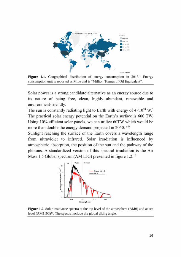
consumption. Figure 1.1 shows that the energy consumption is not
evenly distributed over the world. Based on these facts energy demand
is expanding. According to the statistics in the “Global Energy
Statistical Yearbook 2016” the world’s total energy consumption has
increased by over 2% during the last 15 years1 and it is expected to
increase in the near future.
The extensive use of limited sources of energy like fossil fuels
generates problems such as pollution, global warming, etc. Hence, the
search for new sustainable energy sources is inevitable and crucial.2-4
16
Figure 1.1. Geographical distribution of energy consumption in 2015.1 Energy
consumption unit is reported as Mtoe and is “Million Tonnes of Oil Equivalent”.
Solar power is a strong candidate alternative as an energy source due to
its nature of being free, clean, highly abundant, renewable and
environment-friendly.
The sun is constantly radiating light to Earth with energy of 4×1024 W.5
The practical solar energy potential on the Earth’s surface is 600 TW.
Using 10% efficient solar panels, we can utilize 60TW which would be
more than double the energy demand projected in 2050. 6-9
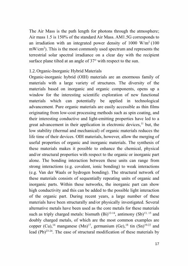
Sunlight reaching the surface of the Earth covers a wavelength range
from ultraviolet to infrared. Solar irradiation is influenced by
atmospheric absorption, the position of the sun and the pathway of the
photons. A standardized version of this spectral irradiation is the Air
Mass 1.5 Global spectrum(AM1.5G) presented in figure 1.2.10
Figure 1.2. Solar irradiance spectra at the top level of the atmosphere (AM0) and at sea
level (AM1.5G)10. The spectra include the global tilting angle.
17
The Air Mass is the path length for photons through the atmosphere;
Air mass 1.5 is 150% of the standard Air Mass. AM1.5G corresponds to
an irradiation with an integrated power density of 1000 W/m2 (100
mW/cm2). This is the most commonly used spectrum and represents the
terrestrial solar spectral irradiance on a clear day with the recipient
surface plane tilted at an angle of 37° with respect to the sun.
1.2. Organic-Inorganic Hybrid Materials
Organic-inorganic hybrid (OIH) materials are an enormous family of
materials with a large variety of structures. The diversity of the
materials based on inorganic and organic components, opens up a
window for the interesting scientific exploration of new functional
materials which can potentially be applied in technological
advancement. Pure organic materials are easily accessible as thin films
originating from low-cost processing methods such as spin coating, and
their interesting conductive and light-emitting properties have led to a
great advancement in their application in electronic devices,11 but, the
low stability (thermal and mechanical) of organic materials reduces the
life time of their devices. OIH materials, however, allow the merging of
useful properties of organic and inorganic materials. The synthesis of
these materials makes it possible to enhance the chemical, physical
and/or structural properties with respect to the organic or inorganic part
alone. The bonding interaction between these units can range from
strong interactions (e.g. covalent, ionic bonding) to weak interactions
(e.g. Van der Waals or hydrogen bonding). The structural network of
these materials consists of sequentially repeating units of organic and
inorganic parts. Within these networks, the inorganic part can show
high conductivity and this can be added to the possible light interaction
of the organic part. During recent years, a large number of these
materials have been structurally and/or physically investigated. Several
alternative metals have been used as the core metals for these materials
such as triply charged metals: bismuth (Bi)12-14, antimony (Sb)13, 15 and
doubly charged metals, of which are the most common examples are
copper (Cu),16 manganese (Mn)17, germanium (Ge),18 tin (Sn)19-22 and
lead (Pb)23-26. The ease of structural modification of these materials by

18
altering the dimensionality of the inorganic frame or the functionality
of the organic part leads to unique impressive photo-electrochemical
properties, and these materials have shown advanced physical
properties such as a band-gap range leading to a broad spectrum of light
absorption and luminescence, high electron and charge conductivity,
and potential thermal stability.11, 26 These characteristics are the main
inspirations for the application of these materials in modern
optoelectronic devices e.g. solar cells, light-emitting diodes (LEDs),
etc.27, 28 Although some of these materials have amorphous structures,
most of them are crystalline materials.11, 29 Their high degree of
crystallinity means that they can be structurally investigated by
methods such as X-ray diffraction. This thesis focuses on the
relationships between the chemical structures of these materials and
their possible functionality.
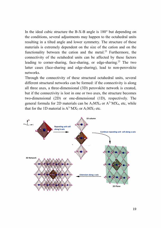
Perovskite structure is one of the important families of large organic-
inorganic hybrid materials. This structure was first found in a purely
inorganic material, calcium titanium oxide (CaTiO3) by Gustav Rose
and it was named perovskite after the Russian mineralogist Lev
Perovski. 30 The structure has the general formula ABX3, where B is a
metal cation and X is an anion either singly charged like a halide, Cl-,
Br-, I- or doubly charged like O2-, S2-, etc. 31 The cation can be either
organic or inorganic. The unit cell is a BX6 octahedron where B is at the
center surrounded by six bonded Xs. The network is built through the
repeating of unit cells by corner connection. The A cations are placed in
the 12 coordinated holes between the consecutive unit cells (See Figure
1.3).
Figure 1.3. The basic unit cell for ABX3 perovskite showing the cubic structure in the
ideal form.
19
In the ideal cubic structure the B-X-B angle is 180° but depending on
the conditions, several adjustments may happen to the octahedral units
resulting in a tilted angle and lower symmetry. The structure of these
materials is extremely dependent on the size of the cation and on the
functionality between the cation and the metal.25 Furthermore, the
connectivity of the octahedral units can be affected by these factors
leading to corner-sharing, face-sharing, or edge-sharing.25 The two
latter cases (face-sharing and edge-sharing), lead to non-perovskite
networks.
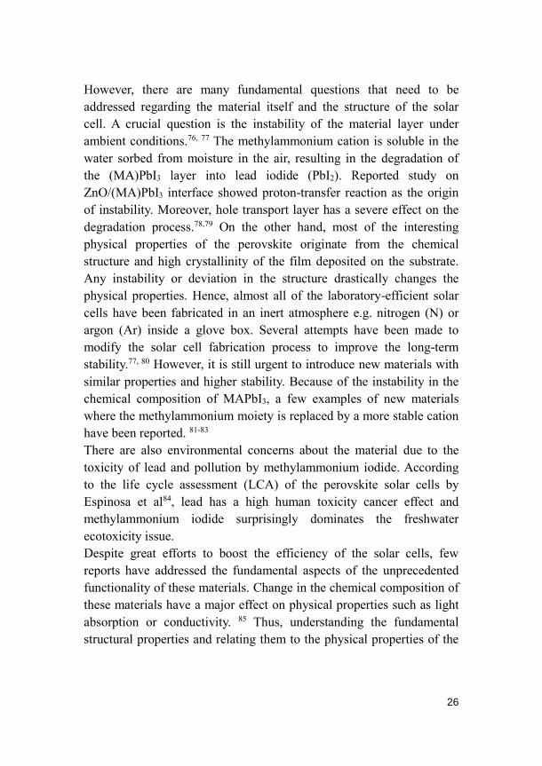
Through the connectivity of these structural octahedral units, several
different structural networks can be formed: if the connectivity is along
all three axes, a three-dimensional (3D) perovskite network is created,
but if the connectivity is lost in one or two axes, the structure becomes
two-dimensional (2D) or one-dimensional (1D), respectively. The
general formula for 2D materials can be A2MX4 or A2+MX4, etc, while
that for the 1D material is A3+MX5 or A3MX5 etc.
Repeating unit cell along b axis
Continue repeating unit cell along a axis
1D column
Extension along c axis
2D Plane
3D Network

20
Figure 1.4. Schematic diagram of the building of structural units from octahedral unit
cells. Three unit cells were added in each axis leading to 3-units 1D rods, 3×3 2D
structural planes, and 3×3×3 3D networks respectively. The connectivity of the unit
cells is through corner-sharing. For the sake of simplicity the A cation is not shown.
Doubly charged cations can also be used to replace two singly charged
A cations, for example in 2D-A2MX4 or 1D-A2M2X6. Several examples
of new structures based on the doubly charged cations have been
introduced and investigated in this work.
In many cases, structural distortions have been observed in the
perovskite structure. The reason for existence of these lower symmetry
structures is that A and/or B ions are not fitted to the size that is
provided by the remaining components.31 A tolerance factor (t) is
determined by the atomic radii of the three components and is
calculated as
𝑡 = (𝑅𝐴+𝑅𝑥)
√2 (𝑅𝑋+𝑅𝐵) (1.1)
where RA, RB, and RX are the atomic radii of the three components in
the perovskite structure. To maintain a perfect cubic three-dimensional
structure, t should be in the range of 0.813˂t˂ 1.107. 31-33
The structural dimensionality is also highly dependent on the ratio
between the metal and the anions, the solvent reactivity and the
temperature and pressure of reaction. The synthetic route is crucial, as it
can lead to different structural and physical properties. Some of the
findings in the present studies cover these facts (see section 3.4).
1.3 Solar Cells
A solar cell or photovoltaic device is a device that absorbs sunlight and
converts it to electricity. The efficiency of this device is the absorbed
light divided by the total illumination, and power conversion efficiency
(η) of a solar cell is the maximum output power (Pmax) divided by the
input power (Pin).
There are different types of solar cells which can be divided into three
different classes or generations of solar cells. They differ in both their
light-harvesting material component and their mechanism of
conversion of light into charge carriers. The first generation of solar

21
cells was based mainly on crystalline silicon, which dominated in
technological applications of photovoltaics because of its high
efficiency and stability. The second generation was based on
amorphous silicon, copper indium gallium selenide (CIGS), or
cadmium telluride (CdTe). They had a lower conversion efficiency than
the first generation but were cheaper. In the third generation, solar cells
are based on the organic materials and were intended to break the
Shockley-Queisser limit, although none actually have achieved this
breakthrough. A wide range of materials can be sensitized for
applications in these solar cells,34, 35 giving several benefits such as the
potential for absorption of a larger fraction of sunlight, cheaper
materials, fabrication simplicity, etc.6 Organic solar cells (OSC), and
dye-sensitized solar cells (DSSC) are examples of these devices. The
working principle of inorganic solar cells (ISC) and DSSC is
summarized in Figure 1.5. The charge separation in junction solar cells
is governed by an electric field generated at the p-n contact intersection. 36 In the dye-sensitized solar cells, light absorption and charge injection
are decoupled from the charge diffusion processes that occur in the
semiconductor.6
Figure 1.5. The basic working principle of the generation of exciton in a. Junction
(inorganic and organic) solar cell and b. Dye-sensitized solar cell.6, 36
1.3.1 Thin Film Solar cells
This family of solar cells also known as second generation solar cells,
which includes amorphous silicon, cadmium telluride (CdTe), cadmium
sulfide(CdS), copper-indium-gallium-selenide (CIGS) and copper-zinc-
tin-sulfide/selenide (CZTS).34 These solar cells have an inorganic light-
absorbing layer with a high extinction coefficient so that a thin film is

22
enough for light absorption. Therefore they are called thin film solar
cells.
The greatest efficiency for crystalline silicon solar cells is reported to
be 25.6%37 but their high production cost is the main disadvantage of
these solar cells in close competition with other solar cell technology.
Solar cells with a much lower production cost, based on a chalcopyrite
(copper, indium, gallium, selenide) absorbing layer are the main
competitor for silicon solar cells.
1.3.1.1 CIGS solar cells
From the first report in 197438 till now the growing interest in CIGS
solar cells resulted in the record efficiency of 21.0%37 on a glass
substrate and over 18% on a flexible substrate. 39-41 To make a typical
CIGS solar cell, a glass substrate is covered by a back contact
molybdenum layer followed by a copper, (indium, gallium) selenide
(sulfur) light-absorbing layer. A cadmium sulfide buffer layer is then
deposited. Finally, solar cell is completed by a layer of zinc oxide
(ZnO) and/or zinc oxide-aluminum on the front surface.39, 42, 43 Vacuum-
based techniques are used to make this type of solar cells. The CIGS
absorbing layer is produced through two processes. In the one-step
method, all materials (CIGS) are deposited in a single step by using
various evaporation processes. In the two-step process, the Copper,
Indium and Gallium are first deposited, and the sulfurization or
selenization sulfur(S) or selenide (Se) process then follows.
1.3.2.2 CdTe/CdS Solar Cells
Solar cells based on a CdTe layer have reached an efficiency of 21.0 %
on a glass substrate.37 Through a vacuum-based method, the conductive
glass substrate is covered by an n-layer of CdS and then a p-layer of
CdTe. The final layer is a back contact, usually aluminium (Al).44 The
structural simplicity of these solar cell means that they are easy to make
and therefore a competitive candidate in solar cells technology.45, 46 In
addition, the band gap for the CdTe is 1.5 eV, very close to the optimum
band gap for the p-n junction solar cells due to their black body limit.47

23
1.3.2. Dye Sensitized Solar Cells (DSSCs)
The manufacture of the efficient solar cells discussed so far requires
specific techniques (such as high vacuum and temperature) and high
purity materials in a clean environment. This leads to the consumption
of a large amount of energy in the production process. DSSC and
perovskite solar cells (PSC-section 1.3.3) are however usually
processed in solution resulting in a lower potential production cost.
A dye-sensitized solar cell consists of a sensitized photo-anode, cathode
and electrolyte (in liquid DSSC) or a solid state hole transport layer (in
solid state DSSC). The anode is based on a metal-oxide high band-gap
semiconductor (e.g. titanium dioxide: TiO2, zinc oxide: ZnO2, etc)
chemically bound to a dye molecule through a sensitization process.
The redox couple (in liquid DSSC) or hole transport layer (in solid state
DSSC) acts as a charge transport bridge between the anode and
cathode. Conventional liquid DSSC uses platinum cathode, and solid
state DSSC has silver as cathode.6, 48-50
As it was presented in Figure 1.5.b, the exciton is produced after light
absorption by the dye molecule. Charge separation occurs first by
electron injection into the conduction band of the oxide semiconductor
/TiO2. Then the oxidized dye is regenerated by either a redox couple or
a hole transport layer. Since the discovery of dye-sensitization by
Moser in the late 19th century51 great efforts have been made to increase
our knowledge and to boost the efficiency of these solar cells, but the
milestone was in 1991, when O’Regan and Grätzel reported a 7%
efficiency for liquid dye sensitized solar cells.50 the current world
record for these solar cells is over 14% 52 for liquid DSSC and 7.7% 53
for solid state DSSC.
1.3.3 Perovskite Solar Cells (PSCs)
A perovskite solar cell is defined as a solar cell which uses mainly
organic-inorganic halide perovskite as light-absorbing component and
in some cases as a hole transporting material.54, 55 Perovskite materials
have been known for many years (Section 1.2) but their application in
solar cells started only recently. Methylammonium lead (II) iodide
[(MA)PbI3] is the most famous material for this application. The cubic

24
structure of (MA)PbI3 was first reported by Weber in 1978.56 The cubic
structure is stable at temperatures above 56 ˚C and at lower
temperatures it transforms to a structural phase with a tetragonal and
orthorhombic structure.23-25, 57 This phase transition is due to the
molecular motion of the methylammonium cation along the C─N
axis.58, 59 Due to the unique properties of this material such as a medium
direct band gap of 1.5eV,24, 57 relatively high absorption coefficient,60
and high carrier mobility61, it is a strong candidate for solar cell
application. In addition, the fact that they are processable in solution
and maintain high crystallinity with few defects in the mesoscopic
semiconductor films62, 63 strengthens their utilization in solar cells. The
solution-based synthesis is one of the cheapest ways to achieve for
efficient crystalline films for these materials, in contrast to high-
vacuum-based synthetic routes which have a high energy consumption.
The high-vacuum-based synthetic routes are still applicable for some
types of thin solar cells e.g. CIGS and CdTe solar cells. The use of
(MA)PbI3 in solar cells started in 2009 by Kojima et al. where they
used it as light-absorbing material in liquid dye-sensitized solar cells.54
The fabricated solar cells had 3.8% conversion efficiency but very poor
stability due to the solubility of the organic cation of the perovskite in
the electrolyte solution.54 The novelty of the work was nevertheless
noticed 2-3 years later and led to the development of perovskite solar
cells. The key turning point was changing from liquid solar cells to
solid state solar cells using a hole transport material. This leads to a
very rapid development in conversion efficiency starting from 9%.64
The conventional solid state hole transport material is a p-type organic
semiconductor named Spiro-OMeTAD (2,2’,7,7’-tetrakis-(N,N-di-p-
methoxy-phentl-amine)9,9’spirobioflurene ) which is still used in the
most efficient perovskite solar cells. Several modifications have been
made to the composition and procedure for solar cells. Mixed halide
perovskite with the composition (MA)PbI3-xClx has gained attention
since Lee et al first used it in solar cells.65 Previously reported data66
have shown that most of the chlorine evaporates during the annealing
step, but a very small portion of the chlorine (depending on the

25
concentration of chlorine reagents) remains in the structure of the
materials. A higher crystallinity was reported for the chlorine-
containing perovskite which led to longer charge carrier diffusion
lengths62 but a band-gap similar to that of the pure iodine perovskite.
The effect of changing the halide composition has been investigated in
several reports mainly leading to band gap changes. The halide moiety
affects the electronic structure rather than the chemical structure,
resulting in a variety of band-gap values while maintaining the 3D
perovskite structure. This observations mainly led to obtaining a higher
open circuit voltage for solar cells67 or band-gap tuning for possible
application of the materials in tandem solar cells. 68, 69
A boost in the efficiency of these solar cells was achieved when the
perovskite film properties were improved by using mixed halide
composition, mixed cation composition, and/or solvent engineering,63,
70-72 reaching a current efficiency of 22.1%.62, 63, 65, 72-75 Currently the
most efficient solar cells are based on a complex light-absorbing layer
composed of triple cation (methylammonium, formamidinium, and
cesium) lead iodide/bromide.70, 75 Some of the major advances in
perovskite solar cell efficiency are summarized in Figure 1.6.
2009 2010 2011 2012 2013 2014 2015 2016 2017
0
5
10
15
20
25
12.3%(KRICT. Korea)
22.1%(KRICT/UNIST. Korea)
19.3%(UCLA. USA)
15.3%(Oxford. UK)
14.1%(EPFL. Switzerland)
10.9%(Oxford. UK)
9.7%(SKKU/EPFL. Korea/Switzerland)
6.5%(SKKU. Korea)
PC
E (
%)
Reported Year
3.8%(T.U. Japan)
Figure 1.6. Development of Perovskite Solar Cells.
Due to this rapid advance in the efficiency of the solar cells, there is an
urgent need to work on the industrialization of these types of solar cells.
26
However, there are many fundamental questions that need to be
addressed regarding the material itself and the structure of the solar
cell. A crucial question is the instability of the material layer under
ambient conditions.76, 77 The methylammonium cation is soluble in the
water sorbed from moisture in the air, resulting in the degradation of
the (MA)PbI3 layer into lead iodide (PbI2). Reported study on
ZnO/(MA)PbI3 interface showed proton-transfer reaction as the origin
of instability. Moreover, hole transport layer has a severe effect on the
degradation process.78,79 On the other hand, most of the interesting
physical properties of the perovskite originate from the chemical
structure and high crystallinity of the film deposited on the substrate.
Any instability or deviation in the structure drastically changes the
physical properties. Hence, almost all of the laboratory-efficient solar
cells have been fabricated in an inert atmosphere e.g. nitrogen (N) or
argon (Ar) inside a glove box. Several attempts have been made to
modify the solar cell fabrication process to improve the long-term
stability.77, 80 However, it is still urgent to introduce new materials with
similar properties and higher stability. Because of the instability in the
chemical composition of MAPbI3, a few examples of new materials
where the methylammonium moiety is replaced by a more stable cation
have been reported. 81-83
There are also environmental concerns about the material due to the
toxicity of lead and pollution by methylammonium iodide. According
to the life cycle assessment (LCA) of the perovskite solar cells by
Espinosa et al84, lead has a high human toxicity cancer effect and
methylammonium iodide surprisingly dominates the freshwater
ecotoxicity issue.
Despite great efforts to boost the efficiency of the solar cells, few
reports have addressed the fundamental aspects of the unprecedented
functionality of these materials. Change in the chemical composition of
these materials have a major effect on physical properties such as light
absorption or conductivity. 85 Thus, understanding the fundamental
structural properties and relating them to the physical properties of the

27
material is a crucial step to meet the challenge of making new
materials.

28
1.4. The aim of thesis Organic-inorganic halide (OIH) materials are a family of materials that
have attracted a lot of interest in several fields, from fundamental
studies to their possible technological applications. Among the OIH
materials, methylammonium lead (II) iodide perovskite has contributed
enormously to the advancement of solar cell research, but some
fundamental question regarding the properties of these materials need
to be addressed. Their poor stability toward heat and moisture is one of
the main questions. The methylammonium moiety shows very low
stability and dissolves in water from moisture in the air or evaporates at
high temperature, and this leaves PbI2 with completely different
chemical and physical properties. In the present work, attempts have
been made to produce new materials with new chemical structures.
Several new OIH lead (II) halide materials have been synthesized and
characterized. The new materials were based on varying the cation
moiety in the methylammonium lead(II) halide perovskite. These
materials showed very high stability compare to methylammonium
based material. Detailed structural information was obtained by single
crystal X-ray characterization, followed by X-ray powder diffraction
and in some cases Raman spectroscopy, showing whether these
materials crystalized in three-dimensions networks, two-dimensional
planes, or one-dimensional columns. Examples of perovskite and non-
perovskite structures were obtained. The stability of the new materials
was assessed and compared with that of methylammonium lead(II)
iodide. Change in the structure has effect on the physical properties of
these materials and investigation of these properties is one of the main
aims of this work. Several methods were used to investigate physical
properties such as conductivity, and light absorption. Higher bandgaps
and lower conductivities were obtained for the lower dimensional
structures. This originates from the limited atomic connection for these
material compare to convention three dimensional methylammonium
lead(II) iodide. Several X-ray spectroscopy techniques have been used
to investigate the electronic structure of these materials and track the
changes due to changes in the chemical structure. The electronic
structures of new materials were thoroughly investigated near both
29
valence bands and conduction bands, and the electronic structures were
related to their chemical structures, to show the effect of bonding
environment and local coordination in the valence band and conduction
band compositions.
The functionality of these materials in the solar cells has finally been
investigated. The efficiency of the fabricated solar cells was up to
1.1%. Despite rather high band-gap values for these materials, the
recorded efficiencies were impressive. As a first step, the solar cells
were prepared based on the optimized condition for the conventional
perovskite solar cells. Further improvement can be expected with
device engineering.
In total, the main aim of this thesis is to present a comprehensive
database for the structural and physical properties of these materials,
and to relate the functionality of the materials in the solar cells to these
properties.

30
2. Experimental Methods & Characterization Techniques
2.1. Material Synthesis and Crystal growth
Solution techniques are the most feasible methods for the synthesis and
crystal growth of the OIH materials. Hence, a feasible way to make
OIH lead-based perovskite materials is to mix lead halide with the salt
of an organic halide in a suitable solvent. Based on the solubility of the
organic and inorganic components, dimethylformamide (DMF),
gamma-Butyrolactone (GBL), and water (H2O) have been used. The
important physical properties of these solvents for the synthesis of OIH
materials are presented in table 2.1. Hydriodic acid (HI) has also been
used as additive to some of aqueous solutions.
Table 2.1. Properties of solvents used for the synthesis of OIH materials.86, 87
Boiling point
(°C)
Vapor pressure
(mmHg) at 20 °C
Viscosity
(cP)
DMF 153 2.7 0.92
GBL 204 1.5 1.9
H2O 100 17.5 1.00
Depending on the activities of the components and the products,
different stoichiometries of starting materials were chosen to initiate the
synthesis. Optimization of the temperature and time is necessary for
completion of the reaction in the solvent. Figure 2.1 illustrates the
synthetic routes which have been used in this work.
Figure 2.1. Schematic diagram of the synthesis of OIH lead halide materials.

31
Chemicals were purchased from Sigma-Aldrich unless otherwise stated.
Hydriodic acid was purchased from Alfa Aesar. For the synthesis of the
mono-ammonium iodide salt, the 1:1 mole equivalent stoichiometry of
the HI (57% w/w in water with 1.5% hypophosphorous acid as
stabilizer) was mixed with the relevant alkylamine. For
methylammonium iodide (MAI), ethylammonium iodide (EAI), and
propylammonium iodide (PAI), 15 mL of HI was mixed with 13.9 mL
of methyl amine(40% w/w in methanol), 10.8mL of ethylamine (70%
in water), or 11.2 mL of propylamine (>99%). For methylammonium
bromide, hydrobromic acid (15.3 mL of 48 wt. % in water) was mixed
with methylamine (14.1 mL of 40% methyl amine in methanol).
The solutions were stirred at 0°C for two hours, and the
alkylammonium halide salts were recovered by evaporation of the
solvent at 50°C using a rotary evaporator. Products were washed three
times with diethylether (≥99.0%), followed by drying at 60°C
overnight:
(2.1)
The same procedure was used for the preparation of methyl ammonium
bromide, where 15.3 mL hydrobromic acid (48 wt. % in water) was
mixed with the 14.1 mL methylamine (40% in methanol).
For the preparation of diammonium iodide salts, 1 mole equivalent of
the relevant alkyldiamine was mixed with 2 mole equivalents of
hydriodic acid. For the preparation of butyldiammonium iodide
(BdAI2), hexyldiammonium iodide (HdAI2), and octyldiammonium
iodide (OdAI2), 3.18g of 1,4-diaminobutane (99%), 4.22 g of 1,6-
diaminohexane (98%), or 5.30g of 1,8-diaminooctane (98%) were
mixed with 13.4 g of HI (57% w/w in water with 1.5%
hypophosphorous acid as stabilizer). The solutions were stirred at 0°C

32
for two hours. After evaporation of solvent, the recovered products
were washed with diethyl ether and dried at 60 °C overnight:
(2.2)
Note: Extra alkylamine or alkyldiamine (~12 w%) was added to the
reaction mixture to avoid any residual HI in the products. The
remaining alkylamine or alkyldiamine were washed away from the
minor residual solution during the evaporation of solvent and washing
with diethyl ether after the reaction.
For materials synthesis, a mixture of the relevant alkyl (di)ammonium
iodide salt and lead iodide salt was stirred in a suitable solvent. The
details of the experimental conditions are given below.
For alkylammonium lead iodide [(A)PbI3], a 1:1 equivalent molar ratio
of alkylammonium iodide and lead iodide (99.999%) (PbI2) were
dissolved in dimethylformamide (anhydrous, 99.8%, DMF). For the
syntheses of methylammonium lead iodide, ethylammonium lead
iodide [(EA)PbI3], and propylammonium lead iodide [(PA)PbI3], 207
mg of MAI, 225 mg EAI, or 243 mg PAI were mixed with 600 mg of
lead(II) iodide in 10 ml of DMF. Methylammonium lead bromide
[(MA)PbBr3], was synthesized through a mixture in 1:1 molar ratio of
145 mg of methylammonium bromide mixed with 477 mg of lead(II)
bromide (PbBr2) (99.999%) in 10ml DMF.
The solutions were stirred at 60°C overnight, and any precipitate was
filtered with a 0.45 µm PTFE syringe filter. The powder products were
recovered by evaporation of the DMF and drying under vacuum
overnight:
(2.3)

33
The procedure for crystal growth of the (A)PbI3 materials has been
reported elsewhere.24 Solutions of (A)PbI3 in GBL with a concentration
of 400 mg mL-1 were heated to 100 °C. After 30 minutes, the solutions
were slowly cooled at a rate of 3 °C per hour. Crystals started growing
at ~70 °C. For (MA)PbI3 crystals were obtained at a temperature above
55°C due to the phase transition at this temperature, but (PA)PbI3
crystals were picked from the solution at room temperature.
For synthesis of one-dimensional butyldiammonium lead iodide
([NH3(CH2)4NH3]Pb2I6, (BdA)Pb2I6), BdAI2 and PbI2 with a mole ratio
of 1:2 were mixed in DMF. 0.739 g of BdAI2 with 1.982g PbI2 were
dissolved in 5ml of DMF, stirred at 60 °C overnight. 1 ml of the
solution was used for crystal growth. When the solvent was evaporated
from the remaining part, a yellow powder remained. The product was
washed with diethyl ether three times, and finally dried under vacuum
overnight:
(2.4)
For the synthesis of two-dimensional alkyldiammonium lead(II) iodide
[(AdA)PbI4] perovskites, a solution in HI of 1 mole equivalent of dAI2
mixed with a solution in HI of 2 mole equivalents of PbI2. For the
synthesis of two-dimensional butyldiammonium lead(II) iodide
[(BdA)PbI4], hexyldiammonium lead(II) iodide [(had)PbI4],
Octyldiammonium lead(II) iodide [(OdA]PbI4], 0.5157g of BdAI2,
0.5577g HdAI2, or 0.5997g OdAI2 was dissolved in 3ml of HI. Each of
these solutions was mixed with a solution of 1.383 g PbI2 in 4 ml HI
and stirred at 90 °C for 1 hour. After evaporation of half (or slightly
more than half) of the solvent, the magnetic stir bar was taken out and
the solution was cooled slowly at a rate of 3-5°C per hour. The cooling
process was continued to -10°C in order to grow single crystals with a
size suitable for crystallography. After removal of some of the
applicable crystals, the remaining precipitate was washed with diethyl
ether and dried under vacuum overnight:

34
(2.5)
Note: To recover powders of the products during evaporation of the
solvent, a small portion of the solution was kept, the precipitate was
filtered and washed with diethyl ether followed by drying under
vacuum.
35
2.2. Chemical Structure Characterization
2.2.1 X-ray Diffraction (XRD)
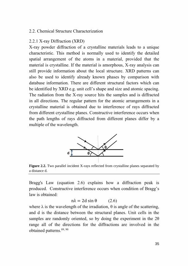
X-ray powder diffraction of a crystalline materials leads to a unique
characteristic. This method is normally used to identify the detailed
spatial arrangement of the atoms in a material, provided that the
material is crystalline. If the material is amorphous, X-ray analysis can
still provide information about the local structure. XRD patterns can
also be used to identify already known phases by comparison with
database information. There are different structural factors which can
be identified by XRD e.g. unit cell’s shape and size and atomic spacing.
The radiation from the X-ray source hits the samples and is diffracted
in all directions. The regular pattern for the atomic arrangements in a
crystalline material is obtained due to interference of rays diffracted
from different crystalline planes. Constructive interference occurs when
the path lengths of rays diffracted from different planes differ by a
multiple of the wavelength.
Figure 2.2. Two parallel incident X-rays reflected from crystalline planes separated by
a distance d.
Bragg's Law (equation 2.6) explains how a diffraction peak is
produced. Constructive interference occurs when condition of Bragg’s
law is obtained:
nλ = 2d sin θ (2.6)
where λ is the wavelength of the irradiation, θ is angle of the scattering,
and d is the distance between the structural planes. Unit cells in the
samples are randomly oriented, so by doing the experiment in the 2θ
range all of the directions for the diffractions are involved in the
obtained patterns.89, 90

36
Powder X-ray diffraction (PXRD)
A PANalytical- X'Pert PRO diffractometer equipped with an X-ray tube
for Cu-Kα radiation has been used. Homogenized fine powder samples
were prepared by grinding in a mortar. For the thin film samples, a
fixed angle for the X-ray radiation was chosen. Diffraction patterns
were obtained over a 2θ range of 5-80° or 5-40°. Depending on the
important peaks, the appropriate 2θ range was chosen for presentation
of the data.
Single Crystal X-ray Diffraction (SXRD)
With this non-destructive technique, detailed information about the
crystalline sample can be obtained, including types of atoms, unit cell
parameters, bond lengths and angles, lattice ordering, etc. During the
analysis, the interaction between X-ray irradiation and the electrons of
the atoms in the single crystal results in an image pattern89 and a
structural report is prepared based on the data collection after solving
and refining the structure.
Two instruments were used for the single crystallography of the
samples.
For characterization of (A)PbI3 and (MA)PbBr3, data were collected on
a Bruker-Nonius KappaCCD diffractometer in the Applied Physical
Chemistry Division at KTH. Corrections of the absorption based on
multiple scans (SADABS) were applied.91 The structures were resolved
using direct methods, and these structures were refined on F2 with
anisotropic thermal parameters for all non-hydrogen atoms. 92
For single crystallography of the (BdA)Pb2I6 and (AdA)PbI4 series, a
Bruker APEXII diffractometer (MoKα radiation) with a CCD detector
at SP Process Development, Södertälje was used. Data collection was
carried at 200K. Crystals were placed on a cryoloop using low-
temperature immersion oil and placed in a N2 cold stream. Data were
recorded by ω-scans and -scans and integrated with the Bruker
SAINT software. A function of the empirical transmission surface was

37
used for fitting and correcting the absorption (Bruker SADABS). To
solve and refine the structures, SHELXS and SHELX were used. A
direct method was used to resolve the structure, resulting in positioning
of the non-hydrogen atoms, after which the positions of the hydrogen
atoms were calculated. Using the anisotropic thermal parameters, final
refinements were achieved for all non-hydrogen atoms.
2.2.2. Raman Spectroscopy
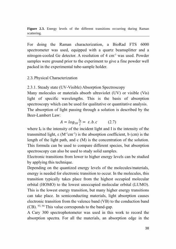
Raman Spectroscopy is based on the inelastic interaction of light with
molecular energy levels. The samples are illuminated by radiation from
a strong light source and a detector collects the scattered light. The
interactions between the incident light and the samples lead to changes
in the frequency of the incident light monitored by the detector.90 The
scattered light with frequencies different from that of the incident light
is presented as a Raman spectrum. Raman spectra are presented as
intensity vs Raman shift in cm-1. Although most of the scattered light
has the frequency of the incident light (elastic scattering), a small part
has a different frequency and is used to construct the Raman spectrum.
Scattered light with a frequency less than that of the incident light
(energy has been absorbed by systems in predominantly the ground
state) represents Stokes lines. On the other hand, recorded scattered
light having a frequency higher than that of the incident light is
considered as anti-Stokes (energy has been emitted by the systems in
predominantly excited states). The Stokes bands represents transitions
from lower to higher excited vibrational levels; hence, they have higher
intensities measured in conventional Raman spectroscopy (there are
simply more systems in the ground state than in excited states).90 Figure
2.3 shows the different Raman shifts.
38
Figure 2.3. Energy levels of the different transitions occurring during Raman
scattering.
For doing the Raman characterization, a BioRad FTS 6000
spectrometer was used, equipped with a quartz beamsplitter and a
nitrogen-cooled Ge detector. A resolution of 4 cm-1 was used. Powder
samples were ground prior to the experiment to give a fine powder well
packed in the experimental tube-sample holder.
2.3. Physical Characterization
2.3.1. Steady state (UV-Visible) Absorption Spectroscopy
Many molecules or materials absorb ultraviolet (UV) or visible (Vis)
light of specific wavelengths. This is the basis of absorption
spectroscopy which can be used for qualitative or quantitative analysis.
The absorption of light passing through a solution is described by the
Beer-Lambert Law:
𝐴 = 𝑙𝑜𝑔10𝐼0
𝐼= 𝜀. 𝑏. 𝑐 (2.7)
where I0 is the intensity of the incident light and I is the intensity of the
transmitted light, ε (M-1cm-1) is the absorption coefficient, b (cm) is the
length of the light path, and c (M) is the concentration of the solution.
This formula can be used to compare different species, but absorption
spectroscopy can also be used to study solid samples.
Electronic transitions from lower to higher energy levels can be studied
by applying this technique.
Depending on the quantized energy levels of the molecules/materials,
energy is needed for electronic transition to occur. In the molecules, this
transition typically takes place from the highest occupied molecular
orbital (HOMO) to the lowest unoccupied molecular orbital (LUMO).
This is the lowest energy transition, but many higher energy transitions
can take place. In semiconducting materials, light absorption causes
electronic transition from the valence band (VB) to the conduction band
(CB). 93, 94 This value corresponds to the band-gap.
A Cary 300 spectrophotometer was used in this work to record the
absorption spectra. For all the materials, an absorption edge in the

39
visible region was observed. For the band-gap calculation the Tauc
equation was used. 95
(𝛼ℎ𝜈)1/𝑛 = 𝐴 (ℎ𝜈 − 𝐸𝑔) (2.8)
where α is the absorption coefficient, h is Planck constant, ν is the
frequency in eV, Eg (eV) is the bandgap and A is normalization
constant. n is equal to ½ and 2 for indirect and direct band-gap
semiconductors respectively.
2.3.2. Conductivity measurements
Electrical conductivity is an important property of materials for solar
cell applications. For semiconducting films, such as the materials used
in this work, the dimensionality of the materials, the orbital overlap
between different atoms, and the crystallinity of the films affect the
conductivity. The conductivity measurements were made with a two
probe device.
Figure 2.4. Schematic diagram of the devices used for the conductivity measurement.
The conductivity value was reported as the average of the values obtained from the
different illustrated measurements.
For preparation of the device, a defined thickness of mesoporous TiO2
layer was coated on a non-conducting glass, followed by spin coating a
layer of the DMF solution of the hybrid materials on top of the TiO2
film. A crystalline film was created by annealing, and a 200nm thick
layer of silver (Ag) was thermally evaporated as the final step. A bias
voltage in the range of -1V to 1V was applied across the two electrodes,
and the photocurrent response was recorded (See Figure 2.4). The slope
of the current-voltage curve was determined as the reverse of resistance
(R) and the conductivity (S.cm-1) was calculated as
𝜎 = 𝑊
𝑅𝐿𝑑 (2.9)
40
where W is the distance between two neighboring Ag contacts, L (cm)
is the length of the Ag contact and d (cm) is the thickness of the film of
TiO2 and hybrid material (Figure 2.2). The thickness was corrected for
the porosity of the TiO2 film by multiplying the thickness of TiO2 by a
factor of 0.6. The thickness of top layer of the material (if any) was
considered in the calculations.96, 97
2.3.3. DFT Calculation
Data based on Density Functional Theory (DFT) were obtained through
collaboration and the author did not personally perform the
calculations. DFT calculations were applied to obtain the band structure
of the two-dimensional materials in paper V. Density of states (DOS)
and partial density of states (PDOS) near the valence band (VB) and
conduction band (CB) edge were obtained. This data support the X-ray
spectroscopic data obtained on the VB and CB and have been used to
create the electronic structure of these materials.
CRYSTAL 09 code was used to perform the theoretical calculations.98
To correct for the exchange-correlation interaction, the Perdew-Burke-
Ernzerhof function was applied.99 Effective core potentials (ECP) of the
Stuttgart-Dresden type [3] were used for the lead and iodine atoms and
the 6-3111G basis sets were used for carbon, nitrogen and hydrogen
atoms.100 To calculate the density of states (DOSs), a k-point mesh was
chosen using Monkhorst−Pack net and a 6×6 shrinking factor was also
used.101
2.3.4. X-ray Spectroscopy
Three techniques based on X-ray illumination have been used in the
work described in papers IV and V. The author has not made these
characterizations. The electronic structure of the materials was
investigated using Hard X-ray Photoelectron Spectropscopy
(HAXPES), High Energy Resolution Fluorescence Detection X-Ray
Absorption Spectroscopy (HERFD-XANES), and Resonant Inelastic
X-ray Scattering (RIXS). Valence band of the OIH samples were
investigated and minor shifts of the VB edges are detected. Occupied

41
and unoccupied states of the iodine were characterized indicating the
iodine orbital contribution in VB and CB.
HAXPES
HAXPES was performed at BESSY II (Helmholtz Zentrum Berlin) at
the KMC-1 beamline using the HIKE end-station.102 The photon energy
was fixed at 4000 eV. A Model R4000 analyzer (Scienta) optimized for
high kinetic energies was used to record the photoelectron kinetic
energies (KE).
HERFD-XANES and RIXS
The HERFD-XANES and RIXS experiments were performed at
beamline ID26 at the European Synchrotron Radiation Facility.103 RIXS
spectra and XANES in the high-energy resolution fluorescence
detection (HERFD) mode were measured using an X-ray emission
spectrometer.104, 105
2.3.5. Nuclear Magnetic Resonance (NMR) Spectroscopy
Solid-state NMR Spectroscopy data have been obtained through
scientific collaborations. A Bruker Avance-HD 500 MHz spectrometer
equipped with a 4 mm CP-MAS probe was used. To record the 14N
spectra, a resonance frequency of 21.7 MHz was applied. The 14N
NMR characterizations were performed on a Bruker Avance-II 300
MHz spectrometer equipped with a 4 mm CP-MAS probe.
Corresponding signals of TMS (for 1H and 13C) and NH4Cl (for 14N)
were set to 0ppm to reference the chemical shifts. In the 207Pb spectra,
the chemical shift was referenced by setting the signal of 207PbSO4 to -
3611 ppm.106
2.4. Photovoltaic Characterization
For solar cell characterization, Current Voltage (IV) and Incident
Photon-to-Current Conversion Efficiency (IPCE) measurements were
made under simulated solar radiation and monochromatic light,
respectively.
42
2.4.1. Current Voltage (IV) Characterization
IV measurement is the most common and essential measurement for
solar cells, where the short circuit current density (Jsc), open circuit
voltage (Voc), fill factor (FF), and power conversation efficiency (PCE
or η) are investigated.
The source is simulated based on the similarity of the emitted spectrum
to the solar AM1.5G spectrum. The intensity of the spectrum is
normally calibrated to 1 Sun corresponding to 1000 Wcm-2 light
intensity. The efficiency of a solar cell (η) is given by the ratio of the
maximum output power (Pmax) to the power of the input light (Pin).
𝜂 = 𝑃𝑚𝑎𝑥
𝑃𝑖𝑛 (2.10)
The measurement is performed by applying a voltage at a desirable
range and recording the photocurrent response. Measuring the voltage
in open circuit conditions gives Voc, and this defines the range of
applied bias voltage between the Voc and zero for the IV measurement.
The highest possible current density under short circuit condition is
measured as Jsc. The theoretical power is defined as PT = Jsc.Voc. FF is
an quality factor in the solar cells that is represented by the shape of the
IV-curve of the solar cell and is defined as the ratio between Pmax and
the product of Jsc and Voc:
𝐹𝐹 = 𝑃𝑚𝑎𝑥
𝑃𝑇=
𝐽𝑚𝑎𝑥𝑉𝑚𝑎𝑥
𝐽𝑠𝑐𝑉𝑜𝑐 (2.11)
and the efficiency of the solar cell can thus be defined as:
𝜂 = 𝐽𝑠𝑐.𝑉𝑜𝑐 .𝐹𝐹
𝑃𝑖𝑛 (2.12)
In this work, after an external potential bias had been applied, the
generated photocurrent was recorded with a Keithley model 2400
digital source meter. A 300 W collimated xenon lamp (Newport) was
used as illumination lamp, and this was calibrated with a certified
silicon solar cell (Fraunhofer ISE) at a light intensity of 100 mW·cm-2
under AM1.5G solar light conditions. A mask with an area of 0.126 cm2
was used during the measurement to expose the solar cells to the
illumination.
43
2.4.2. Incident Photon-to-Current Conversion Efficiency (IPCE)
The IPCE of a solar cell is a wavelength-dependent measure that
describes how many incoming photons are converted to photocurrent.
The solar cell is illuminated by monochromatic light, and the generated
photocurrent is recorded. This photocurrent is dependent on various
processes in the solar cells; the amount of light absorbed (ηabs), the
proportion of the generated electrons that are injected from the light-
absorbing layer to the electron transport layer (ηinj), and the efficiency
of the device in charge collection (ηcoll). The IPCE value is defined as
the product of these three efficiencies.
𝐼𝑃𝐶𝐸 = 𝜂𝑎𝑏𝑠. 𝜂𝑖𝑛𝑗. 𝜂𝑐𝑜𝑙𝑙 (2.13)
The absorbed photon-to-current conversion efficiency (APCE) is
another term used to compare the photovoltaic performances of the
materials.
APCE reflects the ηinj and ηcoll and corrects for the ηabs from IPCE data.
𝐴𝑃𝐶𝐸 = 𝐼𝑃𝐶𝐸
η𝑎𝑏𝑠 (2.14)
Since the materials used in this thesis have shown varying band-gap
and absorption properties, the APCE values were calculated (or
estimated) to compare their charge injection and charge collection
efficiencies. By choosing a wavelength lower than the wavelengths
corresponding to the band-gaps of the materials (e.g. 450nm), APCE
values were calculated from IPCE values.
IPCE spectra were recorded on a computer-controlled unit equipped
with a xenon lamp (Spectral Products ASB-XE-175), a monochromator
(Spectral Products CM110) and a Keithley digital multimeter (Model
2700). A certified silicon solar cell (Fraunhofer ISE) was used to
calibrate the source.

44
3. Result and Discussion
3.1. Structural characterizations and effect of Dimensionality
3.1.1 Introduction
Recent substantial advances in the conversion efficiency of perovskite
solar cells have led to an increased interest in the fundamental
properties of these materials. Structural studies can give useful
information about the atomic positions of the material components and
their arrangement in the structure. Such information may address some
of the fundamental questions about the properties of the materials. In
this section, structural studies on the OIH lead-based materials are
presented. Lead-based metal halide materials have shown different
structural properties with very broad dimensionalities. In the present
work, single crystals obtained by wet methods have been characterized.
3D networks, layered 2D systems, and 1D columns were obtained by
altering the organic cations. X-ray powder diffraction patterns were
obtained for the materials as complementary data for comparison
between the single crystal data and the bulk materials. When the data
were found to be well-matched, single crystallography results were
used as reliable representatives of the bulk materials. The structural
properties of these materials were discussed in relation to the physical
properties (section 3.2.) Several articles have reported the importance
of the solvent in the crystallization of perovskite materials on a TiO2
film. Differences in crystallization affect the film density and
uniformity and this affect the light absorption and more importantly the
conductivity.63, 107, 108 The effect of the solvent on the crystallization of
some of the products has been examined.

45
3.1.2 Three-Dimensional Network As was briefly mentioned in the introduction, the basic perovskite
structure is a systematic repeat of corner-sharing octahedral unit cells of
BX6 and A cations imbedded in a cuboctahedral hole surrounded by 12
X atoms. Among the materials here characterized by X-ray single
crystallography, methylammonium lead (II) iodide [(MA)PbI3] and
methylammonium lead (II) bromide [(MA)PbBr3] have three-
dimensional perovskite structures. The structures of these materials
were first investigated in the 1970s and 1980s23, 56, but after their
application in solar cells, these structures have been more extensively
investigated in recent years.
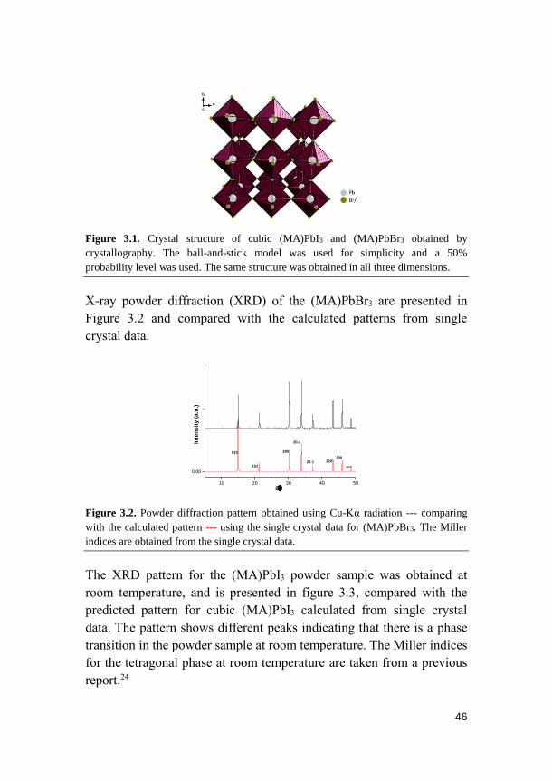
For (MA)PbI3 (at 60°C) and (MA)PbBr3 (at room temperature) cubic
structures with a space group of Pm3m were found in agreement with
previous reports.23, 24 Detailed structural data including lattice
parameters for the two structures are presented in Table 3.1. The
structural details are similar except for some small differences due to
the smaller atomic radius for bromide than for iodide. The distance
between lead atoms is 6.284Å in (MA)PbI3 and 5.913Å in (MA)PbBr3.
The Pb-X-Pb angle in both structures is 180° and X-Pb-X angle is 90°.
Table 3.1. Crystallographic structural data of (MA)PbI3 and (MA)PbBr3.
(MA)PbI3 (MA)PbBr3
Space group P m -3 m P m -3 m
Cell lengths (Å)
a 6.284
b 6.284
c 6.284
a 5.913
b 5.913
c 5.913
Cell angles
α 90.00
β 90.00
γ 90.00
α 90.00
β 90.00
γ 90.00
Cell volume (Å3) 248.15 206.74
Z 1 1
A phase transition of (MA)PbI3 occurs at a temperature below 56°C
resulting in a tetragonal structure with I4/mcm space group,24, 25and
according to our findings (in agreement with previous reports23),
(MA)PbBr3 showed a cubic structure at room temperature. These
findings were confirmed by the X-ray powder diffraction patterns.
46
Figure 3.1. Crystal structure of cubic (MA)PbI3 and (MA)PbBr3 obtained by
crystallography. The ball-and-stick model was used for simplicity and a 50%
probability level was used. The same structure was obtained in all three dimensions.
X-ray powder diffraction (XRD) of the (MA)PbBr3 are presented in
Figure 3.2 and compared with the calculated patterns from single
crystal data.
10 20 30 40 50
0.00103
30022021-1
20-1
200
101
Inte
ns
ity
(a
.u.)
2
010
Figure 3.2. Powder diffraction pattern obtained using Cu-Kα radiation --- comparing
with the calculated pattern --- using the single crystal data for (MA)PbBr3. The Miller
indices are obtained from the single crystal data.
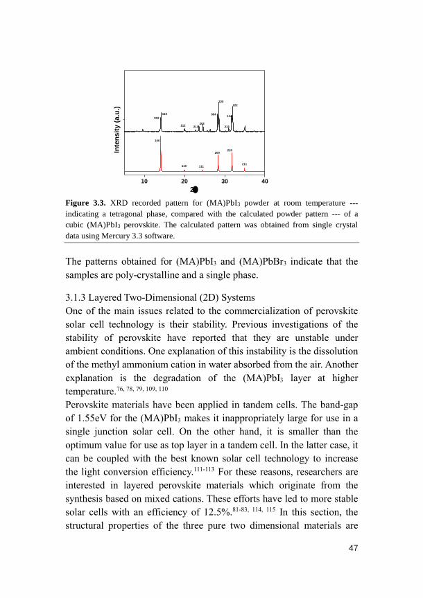
The XRD pattern for the (MA)PbI3 powder sample was obtained at
room temperature, and is presented in figure 3.3, compared with the
predicted pattern for cubic (MA)PbI3 calculated from single crystal
data. The pattern shows different peaks indicating that there is a phase
transition in the powder sample at room temperature. The Miller indices
for the tetragonal phase at room temperature are taken from a previous
report.24
47
10 20 30 40
210
211
200
111110
100
222
114
213
220
004
202211
002
112
110In
ten
sit
y (
a.u
.)
2
Figure 3.3. XRD recorded pattern for (MA)PbI3 powder at room temperature ---
indicating a tetragonal phase, compared with the calculated powder pattern --- of a
cubic (MA)PbI3 perovskite. The calculated pattern was obtained from single crystal
data using Mercury 3.3 software.
The patterns obtained for (MA)PbI3 and (MA)PbBr3 indicate that the
samples are poly-crystalline and a single phase.
3.1.3 Layered Two-Dimensional (2D) Systems
One of the main issues related to the commercialization of perovskite
solar cell technology is their stability. Previous investigations of the
stability of perovskite have reported that they are unstable under
ambient conditions. One explanation of this instability is the dissolution
of the methyl ammonium cation in water absorbed from the air. Another
explanation is the degradation of the (MA)PbI3 layer at higher
temperature.76, 78, 79, 109, 110
Perovskite materials have been applied in tandem cells. The band-gap
of 1.55eV for the (MA)PbI3 makes it inappropriately large for use in a
single junction solar cell. On the other hand, it is smaller than the
optimum value for use as top layer in a tandem cell. In the latter case, it
can be coupled with the best known solar cell technology to increase
the light conversion efficiency.111-113 For these reasons, researchers are
interested in layered perovskite materials which originate from the
synthesis based on mixed cations. These efforts have led to more stable
solar cells with an efficiency of 12.5%.81-83, 114, 115 In this section, the
structural properties of the three pure two dimensional materials are
48
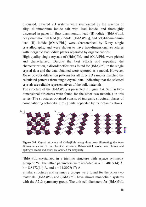
discussed. Layered 2D systems were synthesized by the reaction of
alkyl di-ammonium iodide salt with lead iodide, and thoroughly
discussed in paper II. Butyldiammonium lead (II) iodide [(BdA)PbI4],
hexyldiammonium lead (II) iodide [(HdA)PbI4], and octyldiammonium
lead (II) iodide [(OdA)PbI4] were characterized by X-ray single
crystallography, and were shown to have two-dimensional structures
with inorganic lead iodide planes separated by organic cations.
High quality single crystals of (HdA)PbI4 and (OdA)PbI4 were picked
and characterized. Despite the best efforts and repeating the
characterization, a disorder effect was found for (BdA)PbI4 in the single
crystal data and the data obtained were reported as a model. However,
X-ray powder diffraction patterns for all three 2D samples matched the
calculated patterns from single crystal data, indicating that the selected
crystals are reliable representatives of the bulk materials.
The structure of the (HdA)PbI4 is presented in Figure 3.4. Similar two-
dimensional structures were found for the other two materials in this
series. The structures obtained consist of inorganic structural planes of
corner-sharing octahedral [PbI6] units, separated by the organic cations.
Figure 3.4. Crystal structure of (HdA)PbI4 along three axes illustrating the two-
dimension nature of the chemical structure. Bal-and-stick model was chosen and
hydrogen atoms and bonds are omitted for simplicity.
(BdA)PbI4 crystalized in a triclinic structure with aspace symmetry
group of P1. The lattice parameters were recorded as a = 8.4815(14) Å,
b = 8.8472(14) Å, and c = 11.2028(17) Å.
Similar structures and symmetry groups were found for the other two
materials. (HdA)PbI4 and (OdA)PbI4 have shown monoclinic systems
with the P21/c symmetry group. The unit cell diameters for (HdA)PbI4
a. b. c.
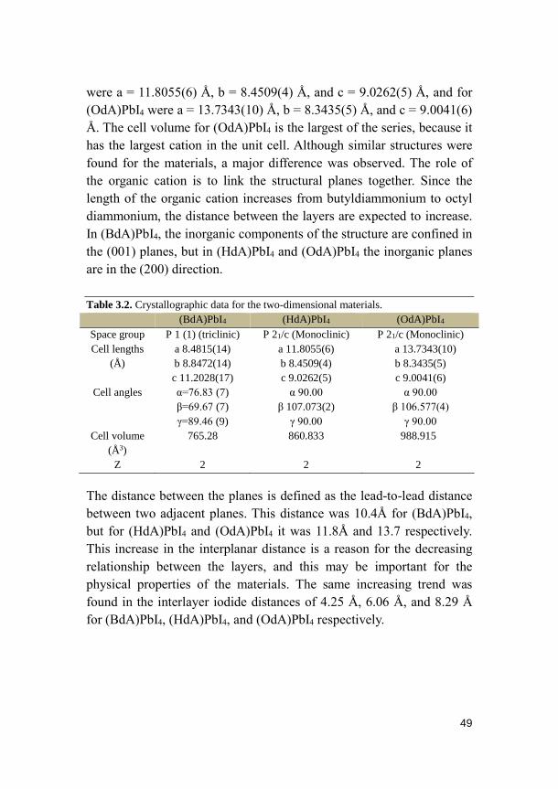
49
were a = 11.8055(6) Å, b = 8.4509(4) Å, and c = 9.0262(5) Å, and for
(OdA)PbI4 were a = 13.7343(10) Å, b = 8.3435(5) Å, and c = 9.0041(6)
Å. The cell volume for (OdA)PbI4 is the largest of the series, because it
has the largest cation in the unit cell. Although similar structures were
found for the materials, a major difference was observed. The role of
the organic cation is to link the structural planes together. Since the
length of the organic cation increases from butyldiammonium to octyl
diammonium, the distance between the layers are expected to increase.
In (BdA)PbI4, the inorganic components of the structure are confined in
the (001) planes, but in (HdA)PbI4 and (OdA)PbI4 the inorganic planes
are in the (200) direction.
Table 3.2. Crystallographic data for the two-dimensional materials.
(BdA)PbI4 (HdA)PbI4 (OdA)PbI4
Space group P 1 (1) (triclinic) P 21/c (Monoclinic) P 21/c (Monoclinic)
Cell lengths
(Å)
a 8.4815(14)
b 8.8472(14)
c 11.2028(17)
a 11.8055(6)
b 8.4509(4)
c 9.0262(5)
a 13.7343(10)
b 8.3435(5)
c 9.0041(6)
Cell angles α=76.83 (7)
β=69.67 (7)
γ=89.46 (9)
α 90.00
β 107.073(2)
γ 90.00
α 90.00
β 106.577(4)
γ 90.00
Cell volume
(Å3)
765.28 860.833 988.915
Z 2 2 2
The distance between the planes is defined as the lead-to-lead distance
between two adjacent planes. This distance was 10.4Å for (BdA)PbI4,
but for (HdA)PbI4 and (OdA)PbI4 it was 11.8Å and 13.7 respectively.
This increase in the interplanar distance is a reason for the decreasing
relationship between the layers, and this may be important for the
physical properties of the materials. The same increasing trend was
found in the interlayer iodide distances of 4.25 Å, 6.06 Å, and 8.29 Å
for (BdA)PbI4, (HdA)PbI4, and (OdA)PbI4 respectively.

50
Figure 3.5. Illustrated structural planes with different distances in the three two-
dimensional materials a. (BdA)PbI4 b. (HdA)PbI4, and c. (OdA)PbI4. The increasing
trend is evident from left to right.
The lead-to-lead distance between two adjacent octahedral units in one
structural plane can also be compared. These distances were found to
be 6.1 Å, 6.16 Å, and 6.14 Å for (BdA)PbI4, (HdA)PbI4, and (OdA)PbI4
respectively, which distances can be compared with 6.28 Å for
(MA)PbI3 and 5.91 Å for (MA)PbBr3.
Another important feature of these two-dimensional structures is the
structural organization of the octahedral units in the planes. The Pb-I-
Pb angles were found to be 150°, 148°, and 147° for (BdA)PbI4,
(HdA)PbI4, and (OdA)PbI4 respectively. By comparing these angles
with the 180° for cubic (MA)PbI3 and (MA)PbBr3, it can be concluded
that there is less ordered structural arrangement in the repeating unit
cells in these 2D systems than in the cubic 3D networks.
Bulk powder X-ray diffraction patterns were obtained at room
temperature and compared with the calculated powder XRD pattern
from single crystal data. The matched patterns in figure 3.6 imply that
the chosen crystals are reliable representative for the bulk of the
material. Hence, structural properties can confidently be used in
discussions of the relationships between structural and physical
properties.
13.73Å 11.81Å
a. (001)
b. (200)
c. (200)
10.38Å

51
10 20 30 40
0
51-14
1-32
31
420
411
023
2223
02
131
32-24
10
013
21-3
400
22-2
221
202
12-2
22-1
30-2
220
31
0
31-1
12-1
012
20-2
020
00210-2
201
111
200
11-1
011
101
100
2
b.
20 40
0
322
213
421
330
113
420
50-21
3-1
411
302
21-3
11-3
401
003
22-2
10-3410
41-1
202
400
31-21
21
30-2
12-1
021
310
31-1
2110
20
300
10-2
21-1
111
11-1
011
101
200
100
2
c.
20 40
0.00
31
43
-203
-1-1
2-2
3
11
-33
13
30
3
22
-1
3-1
11
-3-1
13
11
-1-32
-21
2-2
01
-13
21
3
00
3
21
01
13
21
22
11
20
102
1
1-1
-10
02
1-1
1
11
0
1-1
000
1
Inte
nsit
y (
a.u
.)
2
a.
Figure 3.6. XRD powder patterns --- compared with the calculated patterns --- from
single crystal data of a. (BdA)PbI4 b. (HdA)PbI4 and c. (OdA)PbI4. Miller indices are
generated from single crystal data.
3.1.4 One-Dimensional Rod
In organic-inorganic metal halide materials, one-dimensional structures
consist of metal halide units along chains with organic cations between
the chains. The structural order in these materials is usually less than
that in the 2D and 3D systems and the distance between the inorganic
units is greater.
X-ray single crystallography was performed on the two 1D materials,
propylammonium lead iodide [(PA)PbI3] and 1D-butylammonium lead
iodide [(BdA)Pb2I6]. No suitable single crystal of ethylammonium lead
iodide [(EA)PbI3] was obtained and literature data were used to discuss
its structure. 85
Single crystallography of (PA)PbI3 showed the incorporation of a single
γ-butyrolactone molecule in the unit cell of the crystalline material. A
monoclinic structure with a space group of Cc was recorded with X-ray
single crystal experiment. While Park et al 85 reported an orthorhombic
structure in the space group of Pmmn for (EA)PbI3. Comparing these
structures with the findings for (MA)PbI3 reveals that the addition of
one or two [CH2] groups to the organic cation has a significant impact
on the structural properties of this type of OIH material. The
incorporation of a bulkier cation in the space between the octahedral
[PbI6] in (EA)PbI3 and (PA)PbI3 units leads to a reduction in the
symmetry compared to that of (MA)PbI3. One-dimensional chains were
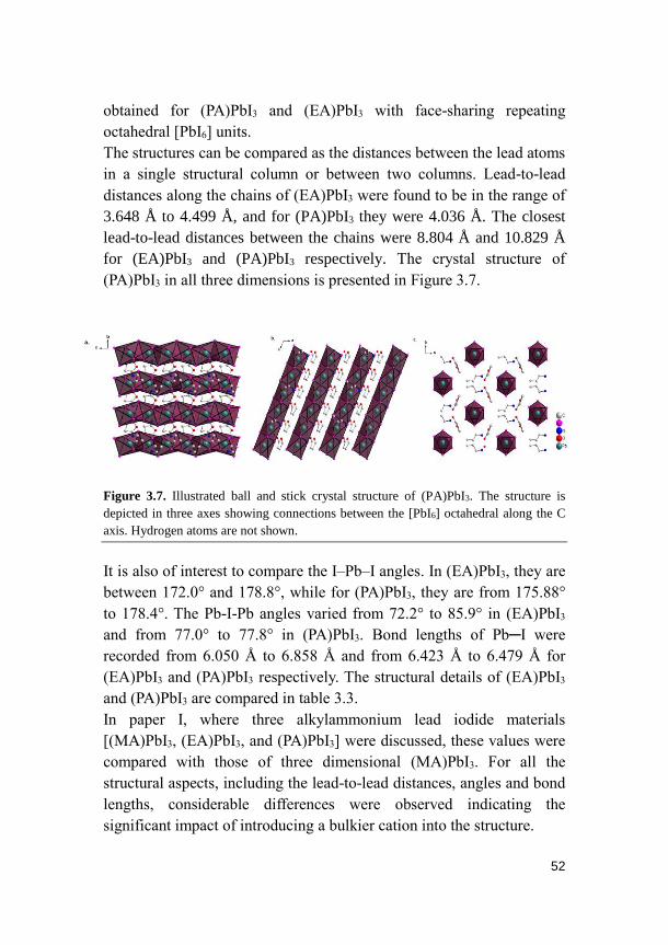
52
obtained for (PA)PbI3 and (EA)PbI3 with face-sharing repeating
octahedral [PbI6] units.
The structures can be compared as the distances between the lead atoms
in a single structural column or between two columns. Lead-to-lead
distances along the chains of (EA)PbI3 were found to be in the range of
3.648 Å to 4.499 Å, and for (PA)PbI3 they were 4.036 Å. The closest
lead-to-lead distances between the chains were 8.804 Å and 10.829 Å
for (EA)PbI3 and (PA)PbI3 respectively. The crystal structure of
(PA)PbI3 in all three dimensions is presented in Figure 3.7.
Figure 3.7. Illustrated ball and stick crystal structure of (PA)PbI3. The structure is
depicted in three axes showing connections between the [PbI6] octahedral along the C
axis. Hydrogen atoms are not shown.
It is also of interest to compare the I–Pb–I angles. In (EA)PbI3, they are
between 172.0° and 178.8°, while for (PA)PbI3, they are from 175.88°
to 178.4°. The Pb-I-Pb angles varied from 72.2° to 85.9° in (EA)PbI3
and from 77.0° to 77.8° in (PA)PbI3. Bond lengths of Pb─I were
recorded from 6.050 Å to 6.858 Å and from 6.423 Å to 6.479 Å for
(EA)PbI3 and (PA)PbI3 respectively. The structural details of (EA)PbI3
and (PA)PbI3 are compared in table 3.3.
In paper I, where three alkylammonium lead iodide materials
[(MA)PbI3, (EA)PbI3, and (PA)PbI3] were discussed, these values were
compared with those of three dimensional (MA)PbI3. For all the
structural aspects, including the lead-to-lead distances, angles and bond
lengths, considerable differences were observed indicating the
significant impact of introducing a bulkier cation into the structure.
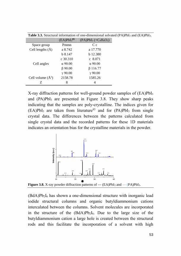
53
10 20 30 40
2.64
1 3 -1
310
4 0 4
4 0 0
3 1 2
2 2 4
3 0 2
1 2 2
2 0 0
2 0 2
2 4 0
2 2 0
2 2 1
0 0 1
200
1 1 2
2 1 4
Inte
ns
ity
(a
.u.)
2
1 0 2
3 1 1
Table 3.3. Structural information of one-dimensional solvated (PA)PbI3 and (EA)PbI3.
(EA)PbI385 (PA)PbI3 (+C4H6O2)
Space group Pmmn C c
Cell lengths (Å) a 8.742
b 8.147
c 30.310
a 17.770
b 12.380
c 8.071
Cell angles α 90.00
β 90.00
γ 90.00
α 90.00
β 116.77
γ 90.00
Cell volume (Å3) 2158.78 1585.26
Z 8 4
X-ray diffraction patterns for well-ground powder samples of (EA)PbI3
and (PA)PbI3 are presented in Figure 3.8. They show sharp peaks
indicating that the samples are poly-crystalline. The indices given for
(EA)PbI3 are taken from literature85 and for (PA)PbI3 from single
crystal data. The differences between the patterns calculated from
single crystal data and the recorded patterns for these 1D materials
indicates an orientation bias for the crystalline materials in the powder.
Figure 3.8. X-ray powder diffraction patterns of --- (EA)PbI3 and --- (PA)PbI3.
(BdA)Pb2I6 has shown a one-dimensional structure with inorganic lead
iodide structural columns and organic butyldiammonium cations
intercalated between the columns. Solvent molecules are incorporated
in the structure of the (BdA)Pb2I6. Due to the large size of the
butyldiammonium cation a large hole is created between the structural
rods and this facilitate the incorporation of a solvent with high
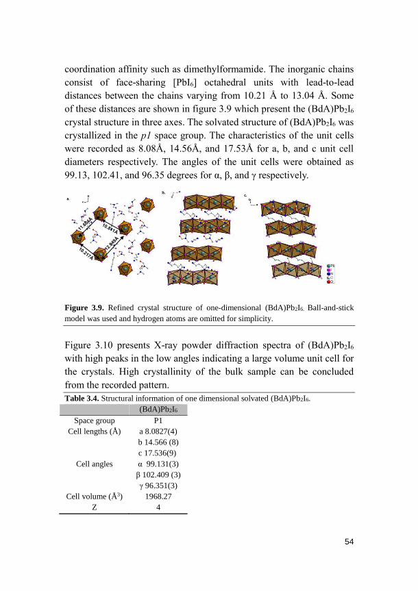
54
coordination affinity such as dimethylformamide. The inorganic chains
consist of face-sharing [PbI6] octahedral units with lead-to-lead
distances between the chains varying from 10.21 Å to 13.04 Å. Some
of these distances are shown in figure 3.9 which present the (BdA)Pb2I6
crystal structure in three axes. The solvated structure of (BdA)Pb2I6 was
crystallized in the p1 space group. The characteristics of the unit cells
were recorded as 8.08Å, 14.56Å, and 17.53Å for a, b, and c unit cell
diameters respectively. The angles of the unit cells were obtained as
99.13, 102.41, and 96.35 degrees for α, β, and γ respectively.
Figure 3.9. Refined crystal structure of one-dimensional (BdA)Pb2I6. Ball-and-stick
model was used and hydrogen atoms are omitted for simplicity.
Figure 3.10 presents X-ray powder diffraction spectra of (BdA)Pb2I6
with high peaks in the low angles indicating a large volume unit cell for
the crystals. High crystallinity of the bulk sample can be concluded
from the recorded pattern.
Table 3.4. Structural information of one dimensional solvated (BdA)Pb2I6.
(BdA)Pb2I6
Space group P1
Cell lengths (Å) a 8.0827(4)
b 14.566 (8)
c 17.536(9)
Cell angles α 99.131(3)
β 102.409 (3)
γ 96.351(3)
Cell volume (Å3) 1968.27
Z 4
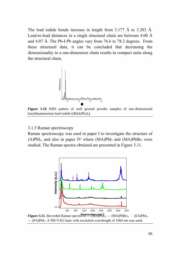
55
10 20 30 40
Inte
nsit
y (
a.u
.)
2
400 800 1200 1600 2000 2400 2800 3200
0.0
Wavenumber (cm-1)
Inte
ns
ity
(a
.u.)
The lead iodide bonds increase in length from 3.177 Å to 3.283 Å.
Lead-to-lead distances in a single structural chain are between 4.00 Å
and 4.07 Å. The Pb-I-Pb angles vary from 76.6 to 78.2 degrees. From
these structural data, it can be concluded that decreasing the
dimensionality to a one-dimension chain results in compact units along
the structural chain.
Figure 3.10 XRD pattern of well ground powder samples of one-dimensional
butyldiammonium lead iodide [(BdA)Pb2I6].
3.1.5 Raman spectroscopy
Raman spectroscopy was used in paper I to investigate the structure of
(A)PbI3, and also in paper IV where (MA)PbI3 and (MA)PbBr3 were
studied. The Raman spectra obtained are presented in Figure 3.11.
Figure 3.11. Recorded Raman spectra of --- (MA)PbI3, --- (MA)PbBr3, --- (EA)PbI3,
--- (PA)PbI3. A ND-YAG laser with excitation wavelength of 1064 nm was used.
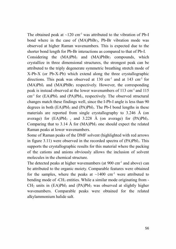
56
The obtained peak at ~120 cm-1 was attributed to the vibration of Pb-I
bond where in the case of (MA)PbBr3, Pb-Br vibration mode was
observed at higher Raman wavenumbers. This is expected due to the
shorter bond length for Pb-Br interactions as compared to that of Pb-I.
Considering the (MA)PbI3 and (MA)PbBr3 compounds, which
crystallize in three dimensional structures, the strongest peak can be
attributed to the triply degenerate symmetric breathing stretch mode of
X-Pb-X (or Pb-X-Pb) which extend along the three crystallographic
directions. This peak was observed at 130 cm-1 and at 143 cm-1 for
(MA)PbI3 and (MA)PbBr3 respectively. However, the corresponding
peak is instead observed at the lower wavenumbers of 113 cm-1 and 115
cm-1 for (EA)PbI3 and (PA)PbI3, respectively. The observed structural
changes match these findings well, since the I-Pb-I angle is less than 90
degrees in both (EA)PbI3 and (PA)PbI3. The Pb-I bond lengths in these
materials are reported from single crystallography to 3.246 Å (on
average) for (EA)PbI3 , and 3.228 Å (on average) for (PA)PbI3.
Comparing that to 3.14 Å for (MA)PbI3 one should expect the related
Raman peaks at lower wavenumbers.
Some of Raman peaks of the DMF solvent (highlighted with red arrows
in figure 3.11) were observed in the recorded spectra of (PA)PbI3. This
supports the crystallographic results for this material where the packing
of the cations and anions obviously allows the inclusion of solvent
molecules in the chemical structure.
The detected peaks at higher wavenumbers (at 900 cm-1 and above) can
be attributed to the organic moiety. Comparable features were obtained
for the samples, where the peaks at ~1400 cm-1 were attributed to
bending mode of -CH3 entities. While a similar mode originating from -
CH2 units in (EA)PbI3 and (PA)PbI3 was observed at slightly higher
wavenumbers. Comparable peaks were obtained for the related
alkylammonium halide salt.

57
3.1.6 Summary
The synthesized materials were successfully investigated representing
three different structural dimensionalities including 3D, 2D, and 1D.
The connectivity of the inorganic network is highly dependent on the
choice of organic cations. Three-dimensional networks were obtained
for (MA)PbI3 and (MA)PbBr3, in accordance with previous findings.
Two-dimensional structures were found for (BdA)PbI4, (HdA)PbI4, and
(OdA)PbI4. These two-dimensional structures differ with respect to the
distances between their structural planes. The inorganic structural plane
consists of a lead iodide system and the organic cations are embedded
between them. (PA)PbI3 and (BdA)Pb2I6 formed one-dimensional
systems, with inorganic lead iodide columns with organic cations
between them.
The lead-to-lead distances were the same along all three axes in the 3D
systems, while in the lower dimensional structures it increased in one or
two directions. The longer distances between the structural units in the
lower dimensional systems allow the incorporation of e.g. solvent
between the unit cells in these directions. The X-ray powder diffraction
patterns of the bulk samples matched the single crystal data. Raman
spectroscopy data confirmed the various structural differences between
the chemical bonds and angles of the different samples.
The detailed structural database obtained has been used in the next
section to discuss the differences in the physical properties of these
materials.

58
400 600
0.000
Ab
so
rpti
on
In
ten
sit
y (
a.u
.)
Wavelength (nm)
(BdA)Pb2I6
(BdA)PbI4
(HdA)PbI4
(OdA)PbI4
500 600 700 800
0.000
Ab
so
rpti
on
In
ten
sit
y (
a.u
.)
Wavelength (nm)
(MA)PbI3
(EA)PbI3
(PA)PbI3
(MA)PbBr3
3.2. Dimensionality impact on Physical Properties
3.2.1. Introduction
After the synthesis and structural characterization of the organic-
inorganic hybrid materials, it was important to determine their physical
properties. Through these experiments, it is possible to relate the
physical properties to the chemical structure of the materials as a step
torwards the possible industrial application of these materials.
The conductivity and light absorption were investigated as two key
properties. Furthermore, the electronic structure was investigated to
see how changes in the chemical bonding through the structural
systems affected the valence band and conduction band edges.
3.2.2. Absorption Spectroscopy and Band-gap
For all of the samples [(MA)PbI3, (MA)PbI3, (EA)PbI3, (PA)PbI3,
(BdA)PbI4, (HdA)PbI4, (OdA)PbI4, and (BdA)Pb2I6] the optical
properties were investigated by UV-Visible absorption spectroscopy. In
the absorption spectra, absorption edges were recorded in the near-IR
and visible regions representing the related energy gaps between the
valence band and conduction band. Figure 3.11 shows the absorption
spectra of thin films of the different materials.
Figure 3.11. UV-Visible absorption spectra of monoammounium and diammonium
(right) OIH films on mesoporous TiO2.
The band-gap values (previously described) have been estimated using
the Tauc equation95:
(𝛼ℎ𝜈)1/𝑛 = 𝐴 (ℎ𝜈 − 𝐸𝑔) (3.1)
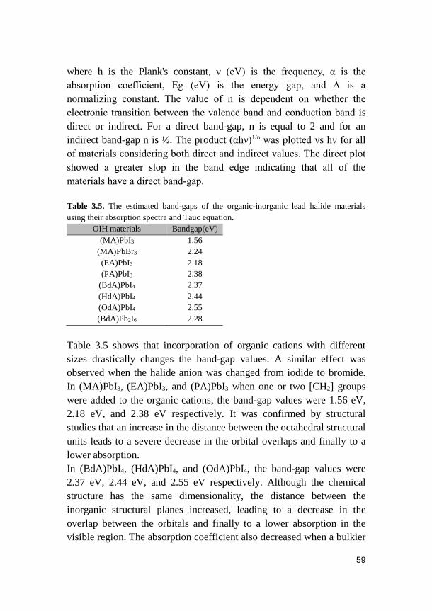
59
where h is the Plank's constant, ν (eV) is the frequency, α is the
absorption coefficient, Eg (eV) is the energy gap, and A is a
normalizing constant. The value of n is dependent on whether the
electronic transition between the valence band and conduction band is
direct or indirect. For a direct band-gap, n is equal to 2 and for an
indirect band-gap n is ½. The product (αhν)1/n was plotted vs hν for all
of materials considering both direct and indirect values. The direct plot
showed a greater slop in the band edge indicating that all of the
materials have a direct band-gap.
Table 3.5. The estimated band-gaps of the organic-inorganic lead halide materials
using their absorption spectra and Tauc equation.
OIH materials Bandgap(eV)
(MA)PbI3 1.56
(MA)PbBr3 2.24
(EA)PbI3 2.18
(PA)PbI3 2.38
(BdA)PbI4 2.37
(HdA)PbI4 2.44
(OdA)PbI4 2.55
(BdA)Pb2I6 2.28
Table 3.5 shows that incorporation of organic cations with different
sizes drastically changes the band-gap values. A similar effect was
observed when the halide anion was changed from iodide to bromide.
In (MA)PbI3, (EA)PbI3, and (PA)PbI3 when one or two [CH2] groups
were added to the organic cations, the band-gap values were 1.56 eV,
2.18 eV, and 2.38 eV respectively. It was confirmed by structural
studies that an increase in the distance between the octahedral structural
units leads to a severe decrease in the orbital overlaps and finally to a
lower absorption.
In (BdA)PbI4, (HdA)PbI4, and (OdA)PbI4, the band-gap values were
2.37 eV, 2.44 eV, and 2.55 eV respectively. Although the chemical
structure has the same dimensionality, the distance between the
inorganic structural planes increased, leading to a decrease in the
overlap between the orbitals and finally to a lower absorption in the
visible region. The absorption coefficient also decreased when a bulkier
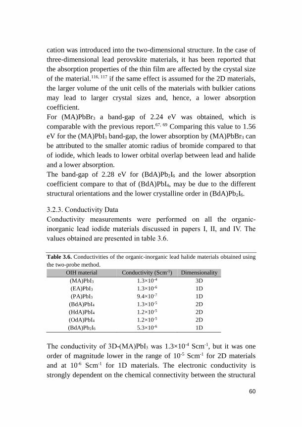
60
cation was introduced into the two-dimensional structure. In the case of
three-dimensional lead perovskite materials, it has been reported that
the absorption properties of the thin film are affected by the crystal size
of the material.116, 117 if the same effect is assumed for the 2D materials,
the larger volume of the unit cells of the materials with bulkier cations
may lead to larger crystal sizes and, hence, a lower absorption
coefficient.
For (MA)PbBr3 a band-gap of 2.24 eV was obtained, which is
comparable with the previous report.67, 69 Comparing this value to 1.56
eV for the (MA)PbI3 band-gap, the lower absorption by (MA)PbBr3 can
be attributed to the smaller atomic radius of bromide compared to that
of iodide, which leads to lower orbital overlap between lead and halide
and a lower absorption.
The band-gap of 2.28 eV for (BdA)Pb2I6 and the lower absorption
coefficient compare to that of (BdA)PbI4, may be due to the different
structural orientations and the lower crystalline order in (BdA)Pb2I6.
3.2.3. Conductivity Data
Conductivity measurements were performed on all the organic-
inorganic lead iodide materials discussed in papers I, II, and IV. The
values obtained are presented in table 3.6.
Table 3.6. Conductivities of the organic-inorganic lead halide materials obtained using
the two-probe method.
OIH material Conductivity (Scm-1) Dimensionality
(MA)PbI3 1.3×10⁻⁴ 3D
(EA)PbI3 1.3×10⁻⁶ 1D
(PA)PbI3 9.4×10⁻⁷ 1D
(BdA)PbI4 1.3×10⁻⁵ 2D
(HdA)PbI4 1.2×10⁻⁵ 2D
(OdA)PbI4 1.2×10⁻⁵ 2D
(BdA)Pb2I6 5.3×10⁻⁶ 1D
The conductivity of 3D-(MA)PbI3 was 1.3×10⁻⁴ Scm-1, but it was one
order of magnitude lower in the range of 10-5 Scm-1 for 2D materials
and at 10-6 Scm-1 for 1D materials. The electronic conductivity is
strongly dependent on the chemical connectivity between the structural
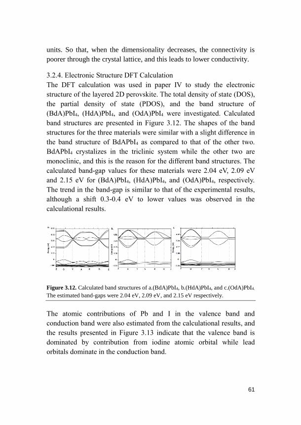
61
units. So that, when the dimensionality decreases, the connectivity is
poorer through the crystal lattice, and this leads to lower conductivity.
3.2.4. Electronic Structure DFT Calculation
The DFT calculation was used in paper IV to study the electronic
structure of the layered 2D perovskite. The total density of state (DOS),
the partial density of state (PDOS), and the band structure of
(BdA)PbI4, (HdA)PbI4, and (OdA)PbI4 were investigated. Calculated
band structures are presented in Figure 3.12. The shapes of the band
structures for the three materials were similar with a slight difference in
the band structure of BdAPbI4 as compared to that of the other two.
BdAPbI4 crystalizes in the triclinic system while the other two are
monoclinic, and this is the reason for the different band structures. The
calculated band-gap values for these materials were 2.04 eV, 2.09 eV
and 2.15 eV for (BdA)PbI4, (HdA)PbI4, and (OdA)PbI4, respectively.
The trend in the band-gap is similar to that of the experimental results,
although a shift 0.3-0.4 eV to lower values was observed in the
calculational results.
Figure 3.12. Calculated band structures of a.(BdA)PbI4, b.(HdA)PbI4, and c.(OdA)PbI4.
The estimated band-gaps were 2.04 eV, 2.09 eV, and 2.15 eV respectively.
The atomic contributions of Pb and I in the valence band and
conduction band were also estimated from the calculational results, and
the results presented in Figure 3.13 indicate that the valence band is
dominated by contribution from iodine atomic orbital while lead
orbitals dominate in the conduction band.
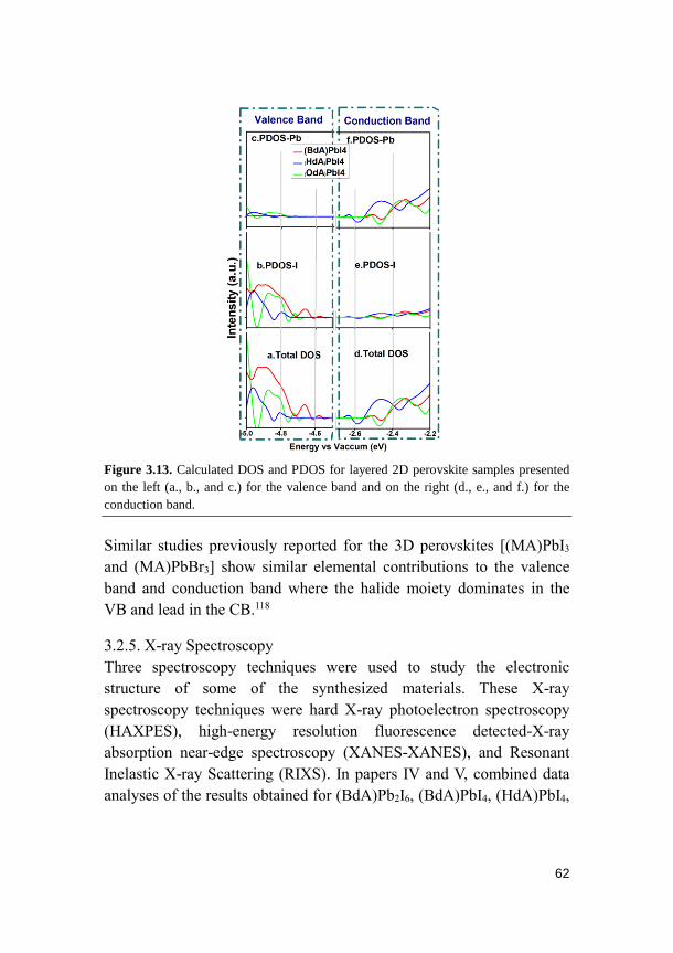
62
Figure 3.13. Calculated DOS and PDOS for layered 2D perovskite samples presented
on the left (a., b., and c.) for the valence band and on the right (d., e., and f.) for the
conduction band.
Similar studies previously reported for the 3D perovskites [(MA)PbI3
and (MA)PbBr3] show similar elemental contributions to the valence
band and conduction band where the halide moiety dominates in the
VB and lead in the CB.118
3.2.5. X-ray Spectroscopy
Three spectroscopy techniques were used to study the electronic
structure of some of the synthesized materials. These X-ray
spectroscopy techniques were hard X-ray photoelectron spectroscopy
(HAXPES), high-energy resolution fluorescence detected-X-ray
absorption near-edge spectroscopy (XANES-XANES), and Resonant
Inelastic X-ray Scattering (RIXS). In papers IV and V, combined data
analyses of the results obtained for (BdA)Pb2I6, (BdA)PbI4, (HdA)PbI4,
63
and (OdA)PbI4 were used to deepen the understanding of the valence
and conduction band configurations of these materials.
The measured iodine 4d and lead 5d core level intensities orbitals were
used to estimate the I/Pb ratio on the surface of each material (Figure
3.14).
Figure 3.14. PES spectra of the I (4d) and Pb (5d) binding energy levels. The
stoichiometry of the materials on the surface has been estimated using the recorded
peak intensities in these spectra.
Appropriate ratios obtained for the materials are presented in table 3.7.
Table 3.7. I/Pb ratio surface analysis estimated from the recorded intensities of the
iodide and lead core levels.
Sample I/Pb Formula
(BdA)PbI4 –[NH3(CH2)4NH3]PbI4 3.82 4
(BdA)Pb2I6 –[NH3(CH2)4NH3]Pb2I6 2.65 3
(HdA)PbI4 –[NH3(CH2)6NH3]PbI4 4.09 4
(OdA)PbI4 – [NH3(CH2)8NH3]PbI4 3.85 4
PbI2 1.78 2
The obtained experimental results matched the expected ratios from the
chemical formula reasonably well. The recorded intensities were
corrected for the photo-ionization cross-section for each element, using
database values. The intensity ratios between different core levels were
calculated from the experimental results.119
The valence band spectra of the materials on the mesoporous TiO2
substrates are presented in the Figure 3.15. These spectra were
calibrated against the Fermi level at zero binding energy. The most
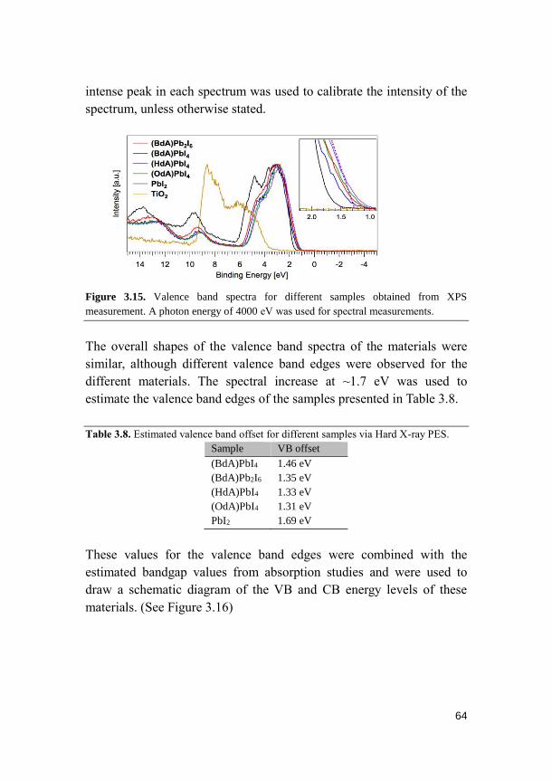
64
intense peak in each spectrum was used to calibrate the intensity of the
spectrum, unless otherwise stated.
Figure 3.15. Valence band spectra for different samples obtained from XPS
measurement. A photon energy of 4000 eV was used for spectral measurements.
The overall shapes of the valence band spectra of the materials were
similar, although different valence band edges were observed for the
different materials. The spectral increase at ~1.7 eV was used to
estimate the valence band edges of the samples presented in Table 3.8.
Table 3.8. Estimated valence band offset for different samples via Hard X-ray PES.
Sample VB offset (BdA)PbI4 1.46 eV (BdA)Pb2I6 1.35 eV
(HdA)PbI4 1.33 eV (OdA)PbI4 1.31 eV PbI2 1.69 eV
These values for the valence band edges were combined with the
estimated bandgap values from absorption studies and were used to
draw a schematic diagram of the VB and CB energy levels of these
materials. (See Figure 3.16)
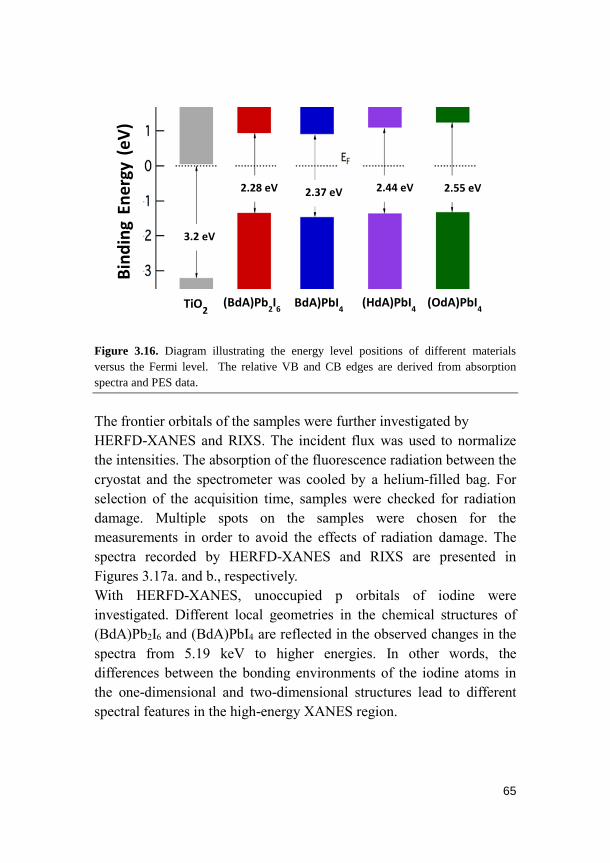
65
Figure 3.16. Diagram illustrating the energy level positions of different materials
versus the Fermi level. The relative VB and CB edges are derived from absorption
spectra and PES data.
The frontier orbitals of the samples were further investigated by
HERFD-XANES and RIXS. The incident flux was used to normalize
the intensities. The absorption of the fluorescence radiation between the
cryostat and the spectrometer was cooled by a helium-filled bag. For
selection of the acquisition time, samples were checked for radiation
damage. Multiple spots on the samples were chosen for the
measurements in order to avoid the effects of radiation damage. The
spectra recorded by HERFD-XANES and RIXS are presented in
Figures 3.17a. and b., respectively.
With HERFD-XANES, unoccupied p orbitals of iodine were
investigated. Different local geometries in the chemical structures of
(BdA)Pb2I6 and (BdA)PbI4 are reflected in the observed changes in the
spectra from 5.19 keV to higher energies. In other words, the
differences between the bonding environments of the iodine atoms in
the one-dimensional and two-dimensional structures lead to different
spectral features in the high-energy XANES region.
(HdA)PbI4 (BdA)PbI
4
2.55 eV
Bin
din
g En
ergy
(eV
)
TiO2 (OdA)PbI
4 (BdA)Pb
2I6
2.44 eV 2.37 eV 2.28 eV
3.2 eV

66
Figure 3.17. a. HERFD-XANES spectra showing the unoccupied states of iodine b.
RIXS spectra showing the occupied states of iodine in the samples.
In the 2D series, small shifts in the absorption edge toward higher
energies were clearly observed in the (BdA)PbI4 ˂ (HdA)PbI4 ˂
(OdA)PbI4 series. Hence, the conduction band edge in the 2D series is
slightly shifted to higher energies with increasing length of the organic
chain. The detected spectra indicate that, although the contribution of
the iodine in the conduction band is small, the effect of the iodine can
be observed in the shifts. The small contributions of iodine in the
conduction bands of the 2D materials were supported by DFT
calculations (see Figure 3.13.e).
RIXS spectra characterize the occupied states of Iodine which were
taken at the first maximum of the iodine L1 absorption edge. The
dipole-allowed transitions from iodine in the 5p orbitals are the origin
of the RIXS spectrum, which shows the partial density of states near
the valence band edge position.
A shift was observed rise at ca. 5.188 in the RIXS spectra of
(BdA)Pb2I6 and (BdA)PbI4, This indicates that the observed valence
band shift of these materials is due mainly to the iodine contribution.
A small wing was observed at ca. 5.18 keV corresponding to the degree
of hybridization between the iodine 5p and lead 6s orbitals. This feature
is expected to exhibit only minor changes in the 2D materials due to the
small differences in the I-Pb-I bonds and angles.
b. a.

67
70 60 50 40 30 20 10 020 15 10 5 0 -5 -10
100 80 60 40 20 0 -20 -40 -60 -80 -100 1200 800 400 0 -400
b) 13
C NMR
ppm
a) 1H NMR
ppm
(CH3NH
3)PbBr
3
c) 14
N NMR
ppm ppm
d) 207
Pb NMR
3.2.6. Nuclear Magnetic Resonance (NMR) Spectroscopy
Through collaboration, NMR spectroscopy was employed in order to
characterize MAPbBr3. NMR spectroscopy, as an element specific
technique, may provide information about the unique local chemical
environment. This may give more information about possible defects in
the lattice of the materials studied. You may also get information
whether the formally equivalent crystal sites in fact also are chemically
equivalent. Recorded 1H NMR, 13C NMR, and 14N NMR spectra of
crystalline MAPbBr3 are depicted in Figure 3.18 a., b., and c.
respectively. In the 1H NMR spectra two signals at ~3.6 ppm and at
~6.6 ppm are attributed to the CH3 and NH3 parts in the
methylammonium cation, respectively. Carbon and Nitrogen single
peaks in the related NMR spectra are representing the carbon atom in
the methyl group and the nitrogen atom in the amine group,
respectively. These finding are in agreement with the previous
reports.120, 121
Figure 3.18. Recoded solid state a. 1H NMR b. 13C NMR c. 14N NMR and d. 207Pb
NMR spectra of methylammonium powder. In d. spectra recorded under both static
(black) and magic angle spinning (red, with 10 kHz spinning rate) conditions are
shown.
The 207Pb NMR spectra of MAPbBr3 recorded under static and spinning
conditions are illustrated in Figure 3.18. d. Comparing the 207Pb NMR
spectra of MAPbBr3 and MAPbI3 a clear difference in chemical shift is
observed (figure 3.19).
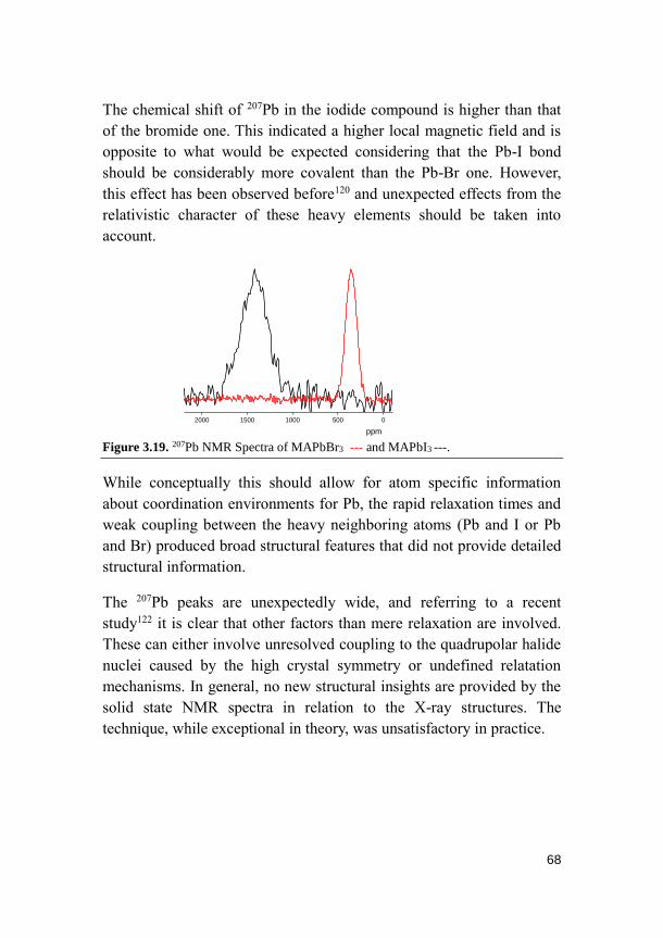
68
2000 1500 1000 500 0
ppm
The chemical shift of 207Pb in the iodide compound is higher than that
of the bromide one. This indicated a higher local magnetic field and is
opposite to what would be expected considering that the Pb-I bond
should be considerably more covalent than the Pb-Br one. However,
this effect has been observed before120 and unexpected effects from the
relativistic character of these heavy elements should be taken into
account.
Figure 3.19. 207Pb NMR Spectra of MAPbBr3 --- and MAPbI3 ---.
While conceptually this should allow for atom specific information
about coordination environments for Pb, the rapid relaxation times and
weak coupling between the heavy neighboring atoms (Pb and I or Pb
and Br) produced broad structural features that did not provide detailed
structural information.
The 207Pb peaks are unexpectedly wide, and referring to a recent
study122 it is clear that other factors than mere relaxation are involved.
These can either involve unresolved coupling to the quadrupolar halide
nuclei caused by the high crystal symmetry or undefined relatation
mechanisms. In general, no new structural insights are provided by the
solid state NMR spectra in relation to the X-ray structures. The
technique, while exceptional in theory, was unsatisfactory in practice.
69
3.2.7 Summary Absorption spectroscopy was successfully applied to obtain the
absorption band edge representing the energy difference between the
valence band and conduction band. Higher band-gap values were
obtained for the lower dimensional materials with the exception of
(BdA)Pb2I6. The highest conductivity value was obtained for MAPbI3
with a three-dimensional network and a highly crystalline film. The
conductivity of the lower dimensional materials was less than that of
3D materials due to the connectivity loss in one or two directions.
In the case of the diammonium-based materials, detailed electronic
structures were presented, providing a comprehensive understanding of
the contributions of the different atomic orbitals in the valence band
and conduction band of each material. The effect of chemical
coordination and bonding environment on the results were discussed.
A strong relationship between the physical properties and the chemical
structure of the materials was observed.
70
3.3. Solar Cell Assembly and Characterization
3.3.1. Solar Cell Architecture
Pilkington TEC15 Fluorine-doped tin-oxide (FTO) coated glass was
used as substrate. The substrates were cleaned by sonication for 30
minutes each in 2% detergent solution, ethanol and acetone. One side of
the substrate with a 3 mm edge was etched using zinc powder and 2M
hydrochloric acid (Figure 3.20.a). A compact blocking layer was
deposited by spin coating at 2000 rpm for 30 seconds of a solution of
titanium isopropoxide in ethanol and hydrochloric acid (a mixture of
175μL of titanium isopropoxide in 1.25 ml ethanol and 175μL of 2 M
HCl in 1.25ml ethanol).76 This was followed by sintering at 500°C for
30 minutes giving a ca. 100 nm thick compact layer. A TiO2 compact
layer was also prepared by another method. The FTO substrates were
pre-heated to 500°C for 15 minutes, and a blocking layer was then
prepared by spray pyrolysis of a 2M titanium isopropoxide solution in
propanol followed by sintering at 500°C for 30 minutes. A solution of
80 mM SpiroOMeTAD, 200 mM 4-tert-butylpyridine (TBP, 99%) and
30 mM bis(trifluoromethane) sulfonimide lithium salt (LiTFSI, 99%,
Io-li-tec) in acetonitrile:chlorobenzene(1:9) was used as a solution of
hole transport material (HTM). The HTM solution was spin coated at
2000 rpm for 30 seconds, and the final layer was deposited by thermal
evaporation of 200 nm silver or 80 nm gold. The solar cells were in all
cases fabricated in ambient air at ambient temperature, except for the
thermal evaporation of the back contact. The humidity varied a lot in
our labratory and it changed from 33% to 56.7% depending on the
season.

71
Figure 3.20. a. the etched substrate for solar cell assembly and b. the schematic
architecture of a solid-state solar cell.
3.3.2. Photovoltaic Characterization
Since the performance of a solar cell is highly dependent on the TiO2
film thickness, the type of back contact (Gold or Silver), and the
ambient conditions (especially for (MA)PbI3-based solar cells), the
solar cell characterization results were discussed in papers I, II, and IV
with respect to the preparation conditions. In these three papers, the
current-voltage characterization was carried out at 10mV/s scan rate for
the bias voltage in order to reduce the risk of hysteresis.123
In paper I, the solar cells were based on alkyammonium lead iodide
[(A)PbI3] with changes in the organic cations by adding one [CH2].
Based on (MA)PbI3-(CH3NH3)PbI3, (EA)PbI3-(CH3CH2NH3)PbI3, and
(PA)PbI3-(CH3CH2CH2NH3)PbI3 as light-absorbing layer, solar cells
were prepared and characterized. In this series, 600 nm thick TiO2 films
were used as electron conductor layer, Spiro-OMeTAD was used as the
HTM, and a 200 nm layer of silver was used as back contact. The
recorded data are presented in table 3.9 and figure 3.21.
a. b.

72
Figure 3.21. a. Photographs of spin-coated DMF-solution of (A)PbI3 on the TiO2
mesoporous layer b. Current-voltage (IV) and c. IPCE curves of the solar cells based on
--- (MA)PbI3, --- (EA)PbI3, and --- (PA)PbI3 as light-absorbing layer. The solar
simulator was calibrated to 1 sun AM1.5G.
The best efficiency was recorded as 7.4% (average of 5 devices) for
(MA)PbI3-based solar cells with a short circuit current density(Jsc) of
16.29 mAcm-2, an open circuit voltage (Voc) of 0.784 V, and a fill
factor (FF) of 0.580. The solar cell efficiency was drastically reduced to
0.26% for (EA)PbI3 and to 0.016% for (PA)PbI3. For (MA)PbI3 , a
relatively low band-gap of 1.56 eV and conductivity of 1.1×10⁻⁴ Scm-1
were obtained. The high performance of the (MA)PbI3 solar cells can
be attributed to their efficient light-harvesting property based on the
low band-gap and rather high extinction coefficient, and to the efficient
charge collection originating from the promoted conductivity. IPCE
curves for the solar cells (see Figure 3.21.c) showed much higher
values for the (MA)PbI3-based solar cells.
a.
0,0 0,2 0,4 0,6 0,8
0,000
0,005
0,010
0,015
0,020
Js
c (
A c
m-2)
V (V)
Jsc
x 10
Jsc
x 100
b.
400 600 800
0
10
20
30
40
50
60
70
80
90
IPC
E (
%)
Wavelength (nm)
IPCE x 10
IPCE x 100
c.
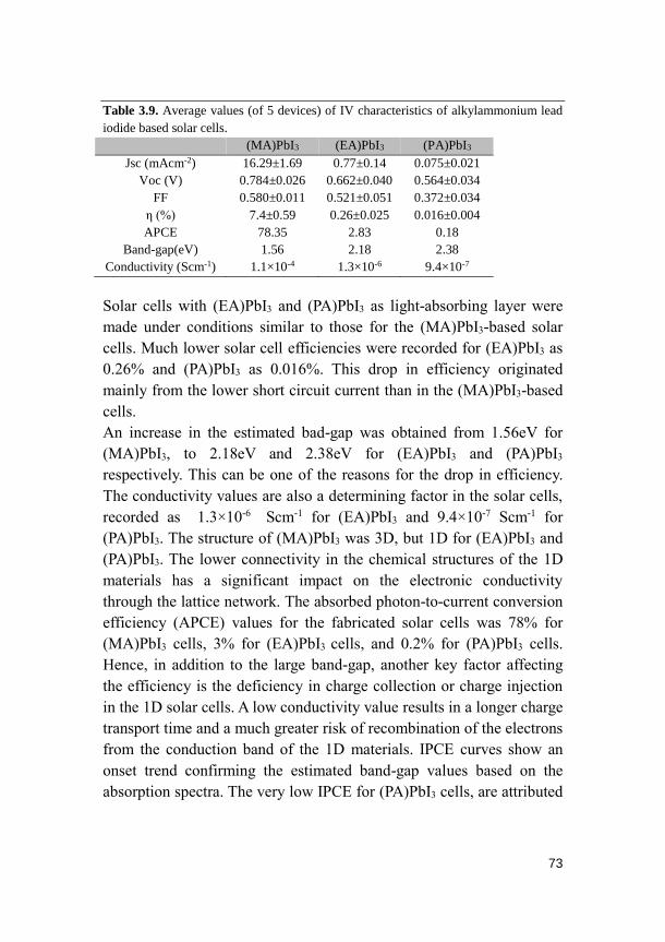
73
Table 3.9. Average values (of 5 devices) of IV characteristics of alkylammonium lead
iodide based solar cells.
(MA)PbI3 (EA)PbI3 (PA)PbI3
Jsc (mAcm-2) 16.29±1.69 0.77±0.14 0.075±0.021
Voc (V) 0.784±0.026 0.662±0.040 0.564±0.034
FF 0.580±0.011 0.521±0.051 0.372±0.034
η (%) 7.4±0.59 0.26±0.025 0.016±0.004
APCE 78.35 2.83 0.18
Band-gap(eV) 1.56 2.18 2.38
Conductivity (Scm-1) 1.1×10⁻⁴ 1.3×10⁻⁶ 9.4×10⁻⁷
Solar cells with (EA)PbI3 and (PA)PbI3 as light-absorbing layer were
made under conditions similar to those for the (MA)PbI3-based solar
cells. Much lower solar cell efficiencies were recorded for (EA)PbI3 as
0.26% and (PA)PbI3 as 0.016%. This drop in efficiency originated
mainly from the lower short circuit current than in the (MA)PbI3-based
cells.
An increase in the estimated bad-gap was obtained from 1.56eV for
(MA)PbI3, to 2.18eV and 2.38eV for (EA)PbI3 and (PA)PbI3
respectively. This can be one of the reasons for the drop in efficiency.
The conductivity values are also a determining factor in the solar cells,
recorded as 1.3×10⁻⁶ Scm-1 for (EA)PbI3 and 9.4×10⁻⁷ Scm-1 for
(PA)PbI3. The structure of (MA)PbI3 was 3D, but 1D for (EA)PbI3 and
(PA)PbI3. The lower connectivity in the chemical structures of the 1D
materials has a significant impact on the electronic conductivity
through the lattice network. The absorbed photon-to-current conversion
efficiency (APCE) values for the fabricated solar cells was 78% for
(MA)PbI3 cells, 3% for (EA)PbI3 cells, and 0.2% for (PA)PbI3 cells.
Hence, in addition to the large band-gap, another key factor affecting
the efficiency is the deficiency in charge collection or charge injection
in the 1D solar cells. A low conductivity value results in a longer charge
transport time and a much greater risk of recombination of the electrons
from the conduction band of the 1D materials. IPCE curves show an
onset trend confirming the estimated band-gap values based on the
absorption spectra. The very low IPCE for (PA)PbI3 cells, are attributed

74
400 500 600 700 800
0
10
20
30
IPC
E (
%)
Wavelength (nm)
IPCE x 100
b.
0.0 0.2 0.4 0.6 0.8
0.0
1.4
2.8
4.2
5.6
7.0
Jsc(m
Acm
-2)
V (v)
a.
Jsc x 10
to the high band-gap, and low conductivity of this material compared to
(EA)PbI3 and (MA)PbI3.
In paper II, the two dimensional materials were used as light-absorbing
layer in the solid state solar cells, and for comparison, (MA)PbI3-based
solar cells were prepared under similar conditions. Table 3.10 presents
the characteristics of these solar cells.
Table 3.10. Recorded IV data for the solar cells based on 2D materials under 1 sun
illumination. Date are compared with (MA)PbI3-based solar cells.
(BdA)PbI4 (HdA)PbI4 (OdA)PbI4 (MA)PbI3
Eff (%) 1.08 0.59 0.012 2.11
Voc (V) 0.870 0.725 0.730 0.805
Jsc (mAcm-2) 2.894 1.735 0.047 5.858
FF 0.430 0.471 0.340 0.449
APCE (%) 24.2 8.1 0.23 31.2
Bandgap (eV) 2.37 2.44 2.55 1.56
Conductivity (Scm-1) 1.3×10⁻⁵ 1.2×10⁻⁵ 1.2×10⁻⁵ 1.3×10⁻⁴
The (BdA)PbI4 cells showed an efficiency of 1.082% with 0.870 V,
2.894 mAcm-2, and 0.430 as open circuit voltage, short circuit current
density, and fill factor respectively. To my knowledge, this is the
highest reported efficiency for a solar cell based on a pure 2D
perovskite light-absorbing layer. For the (HdA)PbI4 and (OdA)PbI4 the
cell conversion efficiency was 0.592% and 0.012% respectively.
Figure 3.22. a. IV, b. IPCE curves for (BdA)PbI4 ─▲─, (HdA)PbI4 ─■─, (OdA)PbI4
─♦─ and (MA)PbI3 ─■─. Solar cells were fabricated under the same conditions.
Mesoprous TiO2 films were used as substrate and the IV curves were recorded under
1sun AM1.5G illumination.

75
5 17 29
0.00
Inte
nsit
y (
a.u
.)
2
a.
5 17 29
0.000
2
c.
5 17 29
0.00
2
b.
The open circuit voltage was 0.870 V for (BdA)PbI4, 0.725 V for
(HdA)PbI4, and 0.732 V for (OdA)PbI4 compared to 0.805 V for
(MA)PbI3 cells. For the (HdA)PbI4 and (OdA)PbI4 cells, a lower Voc
was recorded than for the 3D perovskite cells. A large recombination
loss for (HdA)PbI4 and (OdA)PbI4 cells can originate from exciton
trapping between the layers of the 2D systems. This reduces the
difference in quasi-Fermi levels for TiO2 and Spiro-OMeTAD, and
finally reduces the Voc.124
The band-gap values for these materials were estimated to be 2.37 eV
for (BdA)PbI4, 2.44 eV for (HdA)PbI4, and 2.55 eV for (OdA)PbI4.
Considering the relatively large band-gap for (BdA)PbI4 and the lost
portion of sunlight, an impressive efficiency of 1.08% was obtained for
the related solar cell. Despite small changes in the band-gap values and
the similar conductivities of the three 2D materials, their conversion
efficiency was very low. The low extinction coefficient for the
(OdA)PbI4 could be one explanation for the efficiency drop.
Furthermore, due to the relatively large interplanar distances and larger
volume for the unit cell, crystalline (OdA)PbI4 may not be compatible
with the small pore size of the TiO2 substrate. XRD patterns of the
three 2D materials after deposition on the mesoporous TiO2, show some
level of mismatch for (OdA)PbI4 but the match is better for the other
2D materials (see Figure 3.23).
Figure 3.23. X-ray diffraction patterns of --- powder sample,--- calculated pattern from
single crystal data, and --- spin coated sample on mesoporous TiO2 for a. (BdA)PbI4, b.
(HdA)PbI4 and c. (OdA)PbI4.
The much greater moisture stability of the 2D materials than of the
(MA)PbI3 was a notable property for the solar cell assembly under
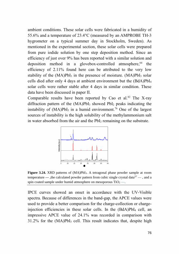
76
5 10 15 20 25 30 35 40
Inte
ns
ity
(a
.u.)
2
ambient conditions. These solar cells were fabricated in a humidity of
55.6% and a temperature of 23.4°C (measured by an AMPROBE TH-3
hygrometer on a typical summer day in Stockholm, Sweden). As
mentioned in the experimental section, these solar cells were prepared
from pure iodide solution by one step deposition method. Since an
efficiency of just over 9% has been reported with a similar solution and
deposition method in a glovebox-controlled atmosphere,64 the
efficiency of 2.11% found here can be attributed to the very low
stability of the (MA)PbI3 in the presence of moisture. (MA)PbI3 solar
cells died after only 4 days at ambient environment but the (BdA)PbI4
solar cells were rather stable after 4 days in similar condition. These
data have been discussed in paper II.
Comparable results have been reported by Cao et al.82 The X-ray
diffraction pattern of the (MA)PbI3 showed PbI2 peaks indicating the
instability of (MA)PbI3 in a humid environment.76 One of the largest
sources of instability is the high solubility of the methylammonium salt
in water absorbed from the air and the PbI2 remaining on the substrate.
Figure 3.24. XRD patterns of (MA)PbI3. A tetragonal phase powder sample at room
temperature --- ,the calculated powder pattern from cubic single crystal data57 --- , and a
spin coated sample under humid atmosphere on mesoporous TiO2 ---.
IPCE curves showed an onset in accordance with the UV-Visible
spectra. Because of differences in the band-gap, the APCE values were
used to provide a better comparison for the charge-collection or charge-
injection efficiencies in these solar cells. In the (BdA)PbI4 cell, an
impressive APCE value of 24.1% was recorded in comparison with
31.2% for the (MA)PbI3 cell. This result indicates that, despite high

77
band-gap values, the (BdA)PbI4 cells have an efficient charge collection
and charge injection. APCE values of 8.1% and 0.23% were obtained
for the (HdA)PbI4 and (OdA)PbI4 cells respectively.
Using a perovskite solar cell in combination with another type of solar
cell in a tandem cell is a novel and interesting idea. Despite the
importance of the idea and previous reports112, 125, 126 a band-gap of 1.56
eV for (MA)PbI3 is not in the best range for coupling to other types of
solar cells. It is lower than the optimal value for use as top layer. For
coupling to silicon with a band-gap of 1.1 eV, a top layer of 1.8 eV is
needed. This combined tandem cell can reach a theoretical efficiency of
42%.127 The band-gap obtained for these 2D perovskite (2.2-2.5 eV)
indicates that it is more appropriate to couple them with for instance
CdTe with a 1.5 eV band-gap. This tandem cell has a theoretical
efficiency of 35%. 127 Since solar cells based on (BdA)PbI4 showed a
promising efficiency, considering their energy diagram, there is
sufficient driving force for electron injection from the conduction band.
Their high thermal and moisture stability can make these materials
more competitive candidates for use in a tandem cell.
In paper IV, one-dimensional (BdA)Pb2I6 solar cells were studied and
compared with the two-dimensional (BdA)PbI4 solar cells. New set of
solar cells were fabricated based on these two materials with only
minor changes in the fabrication process. Compared with the solar cells
previously described, a thinner mesoporous TiO2 layer (~200nm) was
employed with a back contact of gold (Au) instead of silver (Ag). The
detailed structural configuration is presented in the cross-sectional SEM
pictures in Figure 3.25. The recorded characteristic data are presented
in Table 3.11.
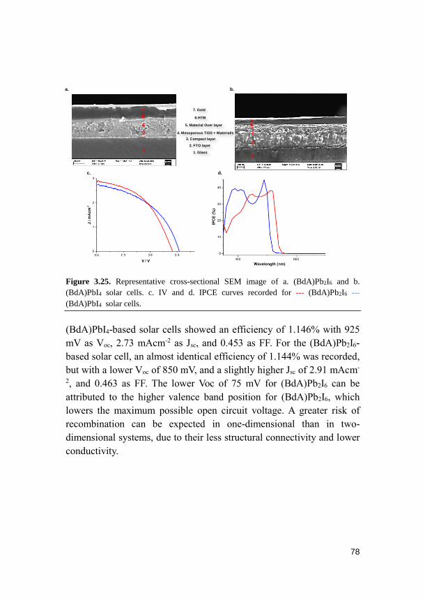
78
Figure 3.25. Representative cross-sectional SEM image of a. (BdA)Pb2I6 and b.
(BdA)PbI4 solar cells. c. IV and d. IPCE curves recorded for --- (BdA)Pb2I6 ---
(BdA)PbI4 solar cells.
(BdA)PbI4-based solar cells showed an efficiency of 1.146% with 925
mV as Voc, 2.73 mAcm-2 as Jsc, and 0.453 as FF. For the (BdA)Pb2I6-
based solar cell, an almost identical efficiency of 1.144% was recorded,
but with a lower Voc of 850 mV, and a slightly higher Jsc of 2.91 mAcm-
2, and 0.463 as FF. The lower Voc of 75 mV for (BdA)Pb2I6 can be
attributed to the higher valence band position for (BdA)Pb2I6, which
lowers the maximum possible open circuit voltage. A greater risk of
recombination can be expected in one-dimensional than in two-
dimensional systems, due to their less structural connectivity and lower
conductivity.
1. Glass
3. Compact layer
2. FTO layer
4. Mesoporous TiO2 + Material/s
5. Material Over layer
6.HTM
7. Gold
1
2
3
5 7
4
1
2
5
4
7
a. b.
c. d.
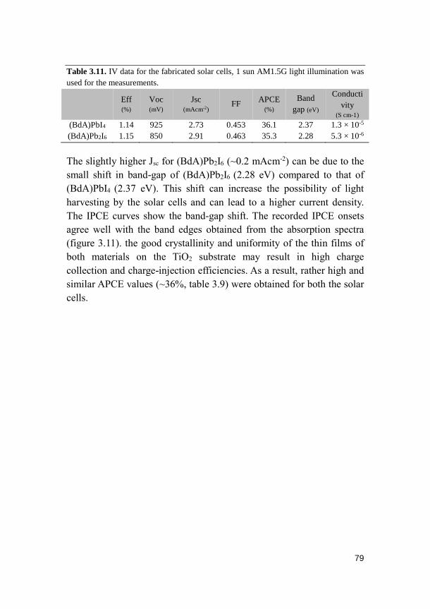
79
Table 3.11. IV data for the fabricated solar cells, 1 sun AM1.5G light illumination was
used for the measurements.
Eff (%)
Voc (mV)
Jsc (mAcm-2)
FF APCE
(%)
Band
gap (eV)
Conducti
vity (S cm-1)
(BdA)PbI4 1.14 925 2.73 0.453 36.1 2.37 1.3 × 10⁻⁵
(BdA)Pb2I6 1.15 850 2.91 0.463 35.3 2.28 5.3 × 10⁻⁶
The slightly higher Jsc for (BdA)Pb2I6 (~0.2 mAcm-2) can be due to the
small shift in band-gap of (BdA)Pb2I6 (2.28 eV) compared to that of
(BdA)PbI4 (2.37 eV). This shift can increase the possibility of light
harvesting by the solar cells and can lead to a higher current density.
The IPCE curves show the band-gap shift. The recorded IPCE onsets
agree well with the band edges obtained from the absorption spectra
(figure 3.11). the good crystallinity and uniformity of the thin films of
both materials on the TiO2 substrate may result in high charge
collection and charge-injection efficiencies. As a result, rather high and
similar APCE values (~36%, table 3.9) were obtained for both the solar
cells.
80
3.3.3. Summary
As an initial application, the new materials were used in solar cells and
characterized. MAPbI3-based solar cells were prepared in each step for
comparison. In a high humidity, stable solar cells based on (BdA)PbI4
and (BdA)Pb2I6 materials showed 1.1% efficiency, compared with the
2.1% efficient MAPbI3 solar cell which showed very low stability
under ambient condition. IPCE spectra were in agreement with the
recorded absorption spectra (presented in previous chapter).
81
4. Concluding remarks
Overall, the work presented in this thesis has focused on the synthesis
of new OIH materials, understanding their properties, and examining
their functionality in solar cells. It provides an insight into the main
structural properties of the characterized materials and relates their
physical properties to these structures, with an emphasis on solar cell
applications.
The chemical structure of the synthesized materials was first
characterized by X-ray techniques leading to the identification of the
specific chemical coordination and bonding environments of the
different components in each material. The materials have been
designed to give a diverse range of dimensionalities. Different groups
of 3D perovskites, 2D perovskites, and 1D non-perovskites were
investigated. The detailed structural properties of these materials were
compared and their differences were discussed. Different bond lengths
and angles were obtained depending on the structural design of the
crystalline network of each material. This led to unique physical
properties for each material.
The introduction of a bulkier cation than methylammonium into the
structure has substantially increased the stability of the material
towards moisture and heat.
A band-gap range from 1.55 eV to 2.55 eV was obtained for the
different materials, indicating a great versatility of the OIH materials
for band-gap engineering. Conductivity measurement confirmed that
when moving from a 3D network to a 2D plane, the conductivity
droped one order of magnitude. The values were even lower for 1D
materials. This decrease in conductivity was attributed to the loss of
connectivity in one and two crystallographic directions in the 2D and
1D systems.
X-ray spectroscopy characterization of the di-ammonium based
materials showed detailed differences in the electronic structures of the
materials. The valence band edge and conduction bad edge were
investigated and showed the dominant contribution of the iodine orbital
in the VB edge and of the lead orbital in the CB edge value. A

82
schematic energy band diagram was presented based on the XPS and
UV-Vis absorption data, and this can be used to identify further
possible applications of these materials in various device architectures.
Characterization of solar cells based on the different materials showed
that methylammonium lead iodide has the highest light conversion
efficiency, but solar cells based on the new di-ammonium materials
have shown up to 1.1% light-conversion efficiency with a substantially
higher stability. The bandgap values of these materials (2.2-2.4 eV),
show that they are suitable for use as top layers in tandem devices.
They can for example be combined with CdTe in a tandem cell to
obtain 35% theoretical efficiency. 128

83
5. Future outlook
To the best of my knowledge, some of the materials presented in this
thesis have here been structurally characterized for the first time. In
addition, most of the lower dimensional materials were subjected to
physical characterization and applied in solar cells for the first time.
The relationship shown between the structure and the function of the
materials can be utilized in the further development of new materials.
New materials can be oriented toward lead-free systems, as this seems
to be an urgent matter in the perovskite research community. In another
approach, one can focus on the improvement of the light-absorption
properties of these materials in order to improve the efficiency of these
types of solar cells.
The synthesized materials have shown a greater stability, and their
band-gap values make them suitable for use as top layer in tandem
devices.
Significant improvements in the efficiency of the solar cells based on
the conventional perovskite have been achieved by choosing mixed
halide compositions for the perovskite. This approach may help to
improve the solar cell efficiency of the materials presented in this
thesis.

84
Acknowledgements
My PhD journey has been concluded to this thesis, but this would not have
happened without the academic, educational and daily life support of many
enthusiastic individuals. Here, I would like to express my sincere appreciation
to you all:
To Associate Prof. James M. Gardner and Prof. Lars Kloo, my great
supervisors who have me the opportunity to work under their supervision. I am
very thankful for your full support, patience, and continuous encouragement.
To my collaborators: Dibya Phuyal, Peng Liu, Dr. Per H. Svensson, Prof.
Håkan Rensmo, Dr. Andreas Fischer, Dr. Bo Xu, Dr. Bertrand Philippe, Minh
Tam Hoang, Prof. Ilwhan Oh, Dr. Sergey V. Dvinskikh, who openly shared
their knowledge and experience with me; thank you so much for your inspiring
scientific discussion and collaborations.
To all my current and former group-mates: Muthuraaman, Jiajia, Azar,
Valentina, Wei, Jiayan, Johnny, Jan; thank you for providing a positive
environment in the group and in the laboratory.
To all my CMD colleagues from Uppsala
To the funding agencies, STandUP for ENERGY, The Swedish Energy
Agency, The Swedish Research Council, the Knut & Alice Wallenberg
Foundation which have financially supported me during my PhD studies.
To all members of “Elburs Futsal Klubb” and all of my friends, my great
appreciation of your positive energy
To my family, both on my side and on Sareh’s side, and to my father’s soul,
who always wanted me educated; thank you for your endless support and all
your help
Last but of course not the least, to my dearest Sareh, my greatest support;
thank you so much for your endless love
And finally, to my little man, Radin, the most incredible gift; thank you!

85
References
1. https://yearbook.enerdata.net/.
2. Vidal-Amaro, J. J.; Østergaard, P. A.; Sheinbaum-Pardo, C., Optimal
energy mix for transitioning from fossil fuels to renewable energy sources – The
case of the Mexican electricity system. Applied Energy 2015, 150, 80-96.
3. McGlade, C.; Ekins, P., The geographical distribution of fossil fuels
unused when limiting global warming to 2 [deg]C. Nature 2015, 517, (7533),
187-190.
4. Long, X.; Naminse, E. Y.; Du, J.; Zhuang, J., Nonrenewable energy,
renewable energy, carbon dioxide emissions and economic growth in China
from 1952 to 2012. Renewable and Sustainable Energy Reviews 2015, 52,
680-688.
5. http://nssdc.gsfc.nasa.gov/planetary/factsheet/sunfact.html.
6. Hagfeldt, A.; Boschloo, G.; Sun, L.; Kloo, L.; Pettersson, H., Dye-
Sensitized Solar Cells. Chemical Reviews 2010, 110, (11), 6595-6663.
7. Service, R. F., Is It Time to Shoot for the Sun? Science 2005, 309,
(5734), 548-551.
8. Potočnik, J., Renewable Energy Sources and the Realities of Setting
an Energy Agenda. Science 2007, 315, (5813), 810-811.
9. Schiermeier, Q.; Tollefson, J.; Scully, T.; Witze, A.; Morton, O., Energy
alternatives: Electricity without carbon. Nature 2008, 454, 816-823.
10. http://www.nrel.gov/solar_radiation/.
11. Mitzi, D. B.; Chondroudis, K.; Kagan, C. R., Organic-inorganic
electronics. IBM Journal of Research and Development 2001, 45, (1), 29-45.
12. Hoye, R. L. Z.; Brandt, R. E.; Osherov, A.; Stevanović, V.; Stranks, S.
D.; Wilson, M. W. B.; Kim, H.; Akey, A. J.; Perkins, J. D.; Kurchin, R. C.;
Poindexter, J. R.; Wang, E. N.; Bawendi, M. G.; Bulović, V.; Buonassisi, T.,
Methylammonium Bismuth Iodide as a Lead-Free, Stable Hybrid Organic–
Inorganic Solar Absorber. Chemistry – A European Journal 2016, 22, (8), 2605-
2610.
13. Mitzi, D. B., Organic−Inorganic Perovskites Containing Trivalent Metal
Halide Layers: The Templating Influence of the Organic Cation Layer.
Inorganic Chemistry 2000, 39, (26), 6107-6113.
14. Park, B.-W.; Philippe, B.; Zhang, X.; Rensmo, H.; Boschloo, G.;
Johansson, E. M. J., Bismuth Based Hybrid Perovskites A3Bi2I9 (A:
Methylammonium or Cesium) for Solar Cell Application. Advanced Materials
2015, 27, (43), 6806-6813.
15. Saparov, B.; Hong, F.; Sun, J.-P.; Duan, H.-S.; Meng, W.; Cameron,
S.; Hill, I. G.; Yan, Y.; Mitzi, D. B., Thin-Film Preparation and Characterization
86
of Cs3Sb2I9: A Lead-Free Layered Perovskite Semiconductor. Chemistry of
Materials 2015, 27, (16), 5622-5632.
16. Willett, R., Structures of the antiferrodistortive layer perovskites
bis(phenethylammonium) tetrahalocuprate(II), halo = Cl-, Br. Acta
Crystallographica Section C 1990, 46, (4), 565-568.
17. Flandrois, S.; Chanh, N. B.; Duplessix, R.; Maris, T.; Négrier, P.,
Structural and magnetic phase transitions in bis-(alkyl ammonium) manganese
tetrachlorides (CnH2n+1NH3)2MnCl4 with In = 5, 7, and 9. physica status solidi
(a) 1995, 149, (2), 697-710.
18. Stoumpos, C. C.; Frazer, L.; Clark, D. J.; Kim, Y. S.; Rhim, S. H.;
Freeman, A. J.; Ketterson, J. B.; Jang, J. I.; Kanatzidis, M. G., Hybrid
Germanium Iodide Perovskite Semiconductors: Active Lone Pairs, Structural
Distortions, Direct and Indirect Energy Gaps, and Strong Nonlinear Optical
Properties. Journal of the American Chemical Society 2015, 137, (21), 6804-
6819.
19. Scaife, D. E.; Weller, P. F.; Fisher, W. G., Crystal preparation and
properties of cesium tin(II) trihalides. Journal of Solid State Chemistry 1974, 9,
(3), 308-314.
20. Shum, K.; Chen, Z.; Qureshi, J.; Yu, C.; Wang, J. J.; Pfenninger, W.;
Vockic, N.; Midgley, J.; Kenney, J. T., Synthesis and characterization of CsSnI3
thin films. Applied Physics Letters 2010, 96, (22), 221903.
21. Chung, I.; Song, J.-H.; Im, J.; Androulakis, J.; Malliakas, C. D.; Li, H.;
Freeman, A. J.; Kenney, J. T.; Kanatzidis, M. G., CsSnI3: Semiconductor or
Metal? High Electrical Conductivity and Strong Near-Infrared
Photoluminescence from a Single Material. High Hole Mobility and Phase-
Transitions. Journal of the American Chemical Society 2012, 134, (20), 8579-
8587.
22. Yu, C.; Chen, Z.; J. Wang, J.; Pfenninger, W.; Vockic, N.; Kenney, J.
T.; Shum, K., Temperature dependence of the band gap of perovskite
semiconductor compound CsSnI3. Journal of Applied Physics 2011, 110, (6),
063526.
23. Poglitsch, A.; Weber, D., Dynamic disorder in
methylammoniumtrihalogenoplumbates (II) observed by millimeter‐wave
spectroscopy. The Journal of Chemical Physics 1987, 87, (11), 6373-6378.
24. Baikie, T.; Fang, Y.; Kadro, J. M.; Schreyer, M.; Wei, F.; Mhaisalkar,
S. G.; Graetzel, M.; White, T. J., Synthesis and crystal chemistry of the hybrid
perovskite (CH3NH3)PbI3 for solid-state sensitised solar cell applications.
Journal of Materials Chemistry A 2013, 1, (18), 5628-5641.
25. Stoumpos, C. C.; Malliakas, C. D.; Kanatzidis, M. G., Semiconducting
Tin and Lead Iodide Perovskites with Organic Cations: Phase Transitions, High
Mobilities, and Near-Infrared Photoluminescent Properties. Inorganic Chemistry
2013, 52, (15), 9019-9038.
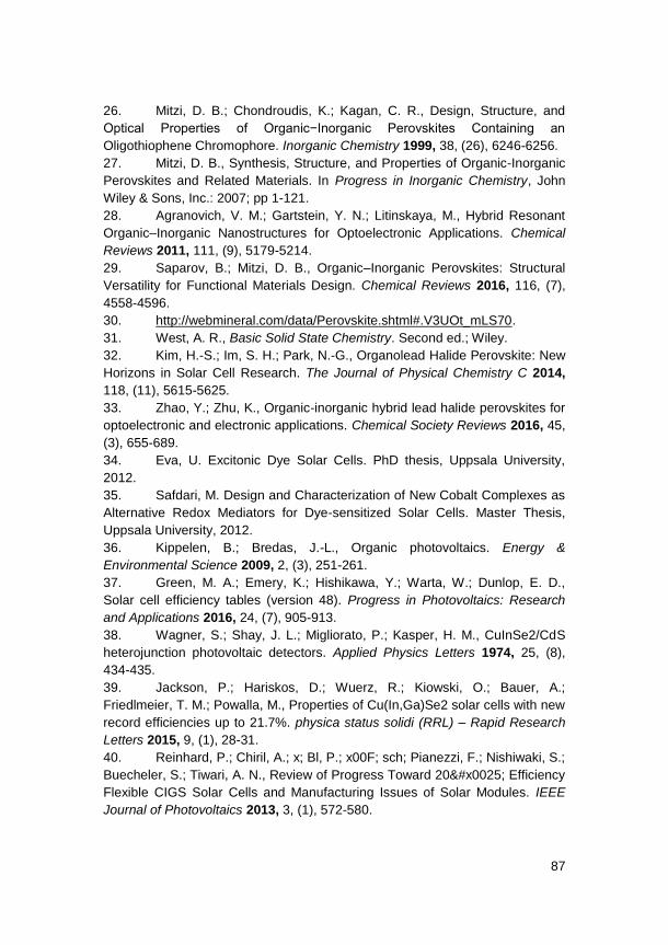
87
26. Mitzi, D. B.; Chondroudis, K.; Kagan, C. R., Design, Structure, and
Optical Properties of Organic−Inorganic Perovskites Containing an
Oligothiophene Chromophore. Inorganic Chemistry 1999, 38, (26), 6246-6256.
27. Mitzi, D. B., Synthesis, Structure, and Properties of Organic-Inorganic
Perovskites and Related Materials. In Progress in Inorganic Chemistry, John
Wiley & Sons, Inc.: 2007; pp 1-121.
28. Agranovich, V. M.; Gartstein, Y. N.; Litinskaya, M., Hybrid Resonant
Organic–Inorganic Nanostructures for Optoelectronic Applications. Chemical
Reviews 2011, 111, (9), 5179-5214.
29. Saparov, B.; Mitzi, D. B., Organic–Inorganic Perovskites: Structural
Versatility for Functional Materials Design. Chemical Reviews 2016, 116, (7),
4558-4596.
30. http://webmineral.com/data/Perovskite.shtml#.V3UOt_mLS70.
31. West, A. R., Basic Solid State Chemistry. Second ed.; Wiley.
32. Kim, H.-S.; Im, S. H.; Park, N.-G., Organolead Halide Perovskite: New
Horizons in Solar Cell Research. The Journal of Physical Chemistry C 2014,
118, (11), 5615-5625.
33. Zhao, Y.; Zhu, K., Organic-inorganic hybrid lead halide perovskites for
optoelectronic and electronic applications. Chemical Society Reviews 2016, 45,
(3), 655-689.
34. Eva, U. Excitonic Dye Solar Cells. PhD thesis, Uppsala University,
2012.
35. Safdari, M. Design and Characterization of New Cobalt Complexes as
Alternative Redox Mediators for Dye-sensitized Solar Cells. Master Thesis,
Uppsala University, 2012.
36. Kippelen, B.; Bredas, J.-L., Organic photovoltaics. Energy &
Environmental Science 2009, 2, (3), 251-261.
37. Green, M. A.; Emery, K.; Hishikawa, Y.; Warta, W.; Dunlop, E. D.,
Solar cell efficiency tables (version 48). Progress in Photovoltaics: Research
and Applications 2016, 24, (7), 905-913.
38. Wagner, S.; Shay, J. L.; Migliorato, P.; Kasper, H. M., CuInSe2/CdS
heterojunction photovoltaic detectors. Applied Physics Letters 1974, 25, (8),
434-435.
39. Jackson, P.; Hariskos, D.; Wuerz, R.; Kiowski, O.; Bauer, A.;
Friedlmeier, T. M.; Powalla, M., Properties of Cu(In,Ga)Se2 solar cells with new
record efficiencies up to 21.7%. physica status solidi (RRL) – Rapid Research
Letters 2015, 9, (1), 28-31.
40. Reinhard, P.; Chiril, A.; x; Bl, P.; x00F; sch; Pianezzi, F.; Nishiwaki, S.;
Buecheler, S.; Tiwari, A. N., Review of Progress Toward 20% Efficiency
Flexible CIGS Solar Cells and Manufacturing Issues of Solar Modules. IEEE
Journal of Photovoltaics 2013, 3, (1), 572-580.
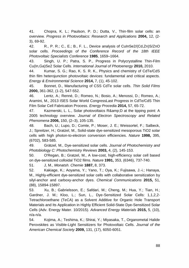
88
41. Chopra, K. L.; Paulson, P. D.; Dutta, V., Thin-film solar cells: an
overview. Progress in Photovoltaics: Research and Applications 2004, 12, (2-
3), 69-92.
42. R., P. R.; C., E.; B., F. L., Device analysis of CuInSe2/(Cd,Zn)S/ZnO
solar cells. Proceedings of the Conference Record of the 18th IEEE
Photovoltaic Specialists Conference 1985, 1659–1664.
43. Singh, U. P.; Patra, S. P., Progress in Polycrystalline Thin-Film
Cu(In,Ga)Se2 Solar Cells. International Journal of Photoenergy 2010, 2010.
44. Kumar, S. G.; Rao, K. S. R. K., Physics and chemistry of CdTe/CdS
thin film heterojunction photovoltaic devices: fundamental and critical aspects.
Energy & Environmental Science 2014, 7, (1), 45-102.
45. Bonnet, D., Manufacturing of CSS CdTe solar cells. Thin Solid Films
2000, 361-362, (1-2), 547-552.
46. Lentz, A.; Renné, D.; Romeo, N.; Bosio, A.; Menossi, D.; Romeo, A.;
Aramini, M., 2013 ISES Solar World CongressLast Progress in CdTe/CdS Thin
Film Solar Cell Fabrication Process. Energy Procedia 2014, 57, 65-72.
47. Kazmerski, L. L., Solar photovoltaics R&D at the tipping point: A
2005 technology overview. Journal of Electron Spectroscopy and Related
Phenomena 2006, 150, (2–3), 105-135.
48. Bach, U.; Lupo, D.; Comte, P.; Moser, J. E.; Weissortel, F.; Salbeck,
J.; Spreitzer, H.; Gratzel, M., Solid-state dye-sensitized mesoporous TiO2 solar
cells with high photon-to-electron conversion efficiencies. Nature 1998, 395,
(6702), 583-585.
49. Grätzel, M., Dye-sensitized solar cells. Journal of Photochemistry and
Photobiology C: Photochemistry Reviews 2003, 4, (2), 145-153.
50. O'Regan, B.; Gratzel, M., A low-cost, high-efficiency solar cell based
on dye-sensitized colloidal TiO2 films. Nature 1991, 353, (6346), 737-740.
51. J, M., Monatsh. Chemie 1887, 8, 373.
52. Kakiage, K.; Aoyama, Y.; Yano, T.; Oya, K.; Fujisawa, J.-i.; Hanaya,
M., Highly-efficient dye-sensitized solar cells with collaborative sensitization by
silyl-anchor and carboxy-anchor dyes. Chemical Communications 2015, 51,
(88), 15894-15897.
53. Xu, B.; Gabrielsson, E.; Safdari, M.; Cheng, M.; Hua, Y.; Tian, H.;
Gardner, J. M.; Kloo, L.; Sun, L., Dye-Sensitized Solar Cells: 1,1,2,2-
Tetrachloroethane (TeCA) as a Solvent Additive for Organic Hole Transport
Materials and Its Application in Highly Efficient Solid-State Dye-Sensitized Solar
Cells (Adv. Energy Mater. 10/2015). Advanced Energy Materials 2015, 5, (10),
n/a-n/a.
54. Kojima, A.; Teshima, K.; Shirai, Y.; Miyasaka, T., Organometal Halide
Perovskites as Visible-Light Sensitizers for Photovoltaic Cells. Journal of the
American Chemical Society 2009, 131, (17), 6050-6051.
89
55. Chung, I.; Lee, B.; He, J.; Chang, R. P. H.; Kanatzidis, M. G., All-solid-
state dye-sensitized solar cells with high efficiency. Nature 2012, 485, (7399),
486-489.
56. Dieter, W., CH3NH3PbX3, ein Pb(II)–system mit kubischer
perowskitstruktur. Zeitschrift für Naturforschung B 1978, 33, 1443–1445.
57. Safdari, M.; Fischer, A.; Xu, B.; Kloo, L.; Gardner, J. M., Structure and
function relationships in alkylammonium lead(ii) iodide solar cells. Journal of
Materials Chemistry A 2015, 3, (17), 9201-9207.
58. Wasylishen, R. E.; Knop, O.; Macdonald, J. B., Cation rotation in
methylammonium lead halides. Solid State Communications 1985, 56, (7), 581-
582.
59. Jung, H. S.; Park, N.-G., Perovskite Solar Cells: From Materials to
Devices. Small 2015, 11, (1), 10-25.
60. Im, J.-H.; Lee, C.-R.; Lee, J.-W.; Park, S.-W.; Park, N.-G., 6.5%
efficient perovskite quantum-dot-sensitized solar cell. Nanoscale 2011, 3, (10),
4088-4093.
61. Kagan, C. R.; Mitzi, D. B.; Dimitrakopoulos, C. D., Organic-Inorganic
Hybrid Materials as Semiconducting Channels in Thin-Film Field-Effect
Transistors. Science 1999, 286, (5441), 945-947.
62. Stranks, S. D.; Eperon, G. E.; Grancini, G.; Menelaou, C.; Alcocer, M.
J. P.; Leijtens, T.; Herz, L. M.; Petrozza, A.; Snaith, H. J., Electron-Hole
Diffusion Lengths Exceeding 1 Micrometer in an Organometal Trihalide
Perovskite Absorber. Science 2013, 342, (6156), 341-344.
63. Jeon, N. J.; Noh, J. H.; Kim, Y. C.; Yang, W. S.; Ryu, S.; Seok, S. I.,
Solvent engineering for high-performance inorganic–organic hybrid perovskite
solar cells. Nat Mater 2014, 13, (9), 897-903.
64. Kim, H.-S.; Lee, C.-R.; Im, J.-H.; Lee, K.-B.; Moehl, T.; Marchioro, A.;
Moon, S.-J.; Humphry-Baker, R.; Yum, J.-H.; Moser, J. E.; Gratzel, M.; Park,
N.-G., Lead Iodide Perovskite Sensitized All-Solid-State Submicron Thin Film
Mesoscopic Solar Cell with Efficiency Exceeding 9%. Sci. Rep. 2012, 2.
65. Lee, M. M.; Teuscher, J.; Miyasaka, T.; Murakami, T. N.; Snaith, H. J.,
Efficient Hybrid Solar Cells Based on Meso-Superstructured Organometal
Halide Perovskites. Science 2012, 338, (6107), 643-647.
66. Unger, E. L.; Bowring, A. R.; Tassone, C. J.; Pool, V. L.; Gold-Parker,
A.; Cheacharoen, R.; Stone, K. H.; Hoke, E. T.; Toney, M. F.; McGehee, M. D.,
Chloride in Lead Chloride-Derived Organo-Metal Halides for Perovskite-
Absorber Solar Cells. Chemistry of Materials 2014, 26, (24), 7158-7165.
67. Edri, E.; Kirmayer, S.; Cahen, D.; Hodes, G., High Open-Circuit
Voltage Solar Cells Based on Organic–Inorganic Lead Bromide Perovskite. The
Journal of Physical Chemistry Letters 2013, 4, (6), 897-902.
68. Jesper Jacobsson, T.; Correa-Baena, J.-P.; Pazoki, M.; Saliba, M.;
Schenk, K.; Gratzel, M.; Hagfeldt, A., Exploration of the compositional space for
90
mixed lead halogen perovskites for high efficiency solar cells. Energy &
Environmental Science 2016, 9, (5), 1706-1724.
69. Noh, J. H.; Im, S. H.; Heo, J. H.; Mandal, T. N.; Seok, S. I., Chemical
Management for Colorful, Efficient, and Stable Inorganic–Organic Hybrid
Nanostructured Solar Cells. Nano Letters 2013, 13, (4), 1764-1769.
70. Bi, D.; Tress, W.; Dar, M. I.; Gao, P.; Luo, J.; Renevier, C.; Schenk, K.;
Abate, A.; Giordano, F.; Correa Baena, J.-P.; Decoppet, J.-D.; Zakeeruddin, S.
M.; Nazeeruddin, M. K.; Grätzel, M.; Hagfeldt, A., Efficient luminescent solar
cells based on tailored mixed-cation perovskites. Science Advances 2016, 2,
(1).
71. Yang, W. S.; Noh, J. H.; Jeon, N. J.; Kim, Y. C.; Ryu, S.; Seo, J.;
Seok, S. I., High-performance photovoltaic perovskite layers fabricated through
intramolecular exchange. Science 2015, 348, (6240), 1234-1237.
72. Jeon, N. J.; Noh, J. H.; Yang, W. S.; Kim, Y. C.; Ryu, S.; Seo, J.;
Seok, S. I., Compositional engineering of perovskite materials for high-
performance solar cells. Nature 2015, 517, (7535), 476-480.
73. Burschka, J.; Pellet, N.; Moon, S.-J.; Humphry-Baker, R.; Gao, P.;
Nazeeruddin, M. K.; Gratzel, M., Sequential deposition as a route to high-
performance perovskite-sensitized solar cells. Nature 2013, 499, (7458), 316-
319.
74. Liu, M.; Johnston, M. B.; Snaith, H. J., Efficient planar heterojunction
perovskite solar cells by vapour deposition. Nature 2013, 501, (7467), 395-398.
75. http://www.nrel.gov/ncpv/images/efficiency_chart.jpg.
76. Pathak, S.; Sepe, A.; Sadhanala, A.; Deschler, F.; Haghighirad, A.;
Sakai, N.; Goedel, K. C.; Stranks, S. D.; Noel, N.; Price, M.; Hüttner, S.;
Hawkins, N. A.; Friend, R. H.; Steiner, U.; Snaith, H. J., Atmospheric Influence
upon Crystallization and Electronic Disorder and Its Impact on the
Photophysical Properties of Organic–Inorganic Perovskite Solar Cells. ACS
Nano 2015, 9, (3), 2311-2320.
77. You, J.; Meng, L.; Song, T.-B.; Guo, T.-F.; Yang, Y.; Chang, W.-H.;
Hong, Z.; Chen, H.; Zhou, H.; Chen, Q.; Liu, Y.; De Marco, N.; Yang, Y.,
Improved air stability of perovskite solar cells via solution-processed metal
oxide transport layers. Nat Nano 2016, 11, (1), 75-81.
78. Yang, J.; Siempelkamp, B. D.; Mosconi, E.; De Angelis, F.; Kelly, T. L.,
Origin of the Thermal Instability in CH3NH3PbI3 Thin Films Deposited on ZnO.
Chemistry of Materials 2015, 27, (12), 4229-4236.
79. Yang, J.; Siempelkamp, B. D.; Liu, D.; Kelly, T. L., Investigation of
CH3NH3PbI3 Degradation Rates and Mechanisms in Controlled Humidity
Environments Using in Situ Techniques. ACS Nano 2015, 9, (2), 1955-1963.
80. Guarnera, S.; Abate, A.; Zhang, W.; Foster, J. M.; Richardson, G.;
Petrozza, A.; Snaith, H. J., Improving the Long-Term Stability of Perovskite

91
Solar Cells with a Porous Al2O3 Buffer Layer. The Journal of Physical
Chemistry Letters 2015, 6, (3), 432-437.
81. Smith, I. C.; Hoke, E. T.; Solis-Ibarra, D.; McGehee, M. D.;
Karunadasa, H. I., A Layered Hybrid Perovskite Solar-Cell Absorber with
Enhanced Moisture Stability. Angewandte Chemie International Edition 2014,
53, (42), 11232-11235.
82. Cao, D. H.; Stoumpos, C. C.; Farha, O. K.; Hupp, J. T.; Kanatzidis, M.
G., 2D Homologous Perovskites as Light-Absorbing Materials for Solar Cell
Applications. Journal of the American Chemical Society 2015, 137, (24), 7843-
7850.
83. Tsai, H.; Nie, W.; Blancon, J.-C.; Stoumpos, C. C.; Asadpour, R.;
Harutyunyan, B.; Neukirch, A. J.; Verduzco, R.; Crochet, J. J.; Tretiak, S.;
Pedesseau, L.; Even, J.; Alam, M. A.; Gupta, G.; Lou, J.; Ajayan, P. M.;
Bedzyk, M. J.; Kanatzidis, M. G.; Mohite, A. D., High-efficiency two-dimensional
Ruddlesden–Popper perovskite solar cells. Nature 2016, advance online
publication.
84. Espinosa, N.; Serrano-Luján, L.; Urbina, A.; Krebs, F. C., Solution and
vapour deposited lead perovskite solar cells: Ecotoxicity from a life cycle
assessment perspective. Solar Energy Materials and Solar Cells 2015, 137,
303-310.
85. Im, J.-H.; Chung, J.; Kim, S.-J.; Park, N.-G., Synthesis, structure, and
photovoltaic property of a nanocrystalline 2H perovskite-type novel sensitizer
(CH3CH2NH3)PbI3. Nanoscale Research Letters 2012, 7, (1), 1-7.
86. Christian, R.; Thomas, W., Solvents and Solvent Effects in Organic
Chemistry. 2010.
87. CRC Handbook of Chemistry and Physics. In 63 ed.; Weast, R. C.,
Ed. CRC press, 1983.
88. Nishikata, E.; Ishii, T.; Ohta, T., Viscosities of aqueous hydrochloric
acid solutions, and densities and viscosities of aqueous hydroiodic acid
solutions. Journal of Chemical & Engineering Data 1981, 26, (3), 254-256.
89. Kimiko, H., Introduction to single crystal X-ray analysis. The Rikago
Journal 2012, 28, (1), 14-18.
90. Peter, A.; Julio, D. P., Physical Chemistry. Seven ed.; Oxford
University Press: 2002.
91. M., S. G., SADABS v.2.10; Program for empirical absorption
correction of area detector data, . University ofGöttingen, Germany 2003.
92. Sheldrick, G., A short history of SHELX. Acta Crystallographica
Section A 2008, 64, (1), 112-122.
93. http://www.rsc.org/learn-
chemistry/resource/res00000941/spectroscopy-in-a-suitcase-uv-vis-teacher-
resources?cmpid=CMP00001304.
94. http://www.chemguide.co.uk/analysis/uvvisiblemenu.html.
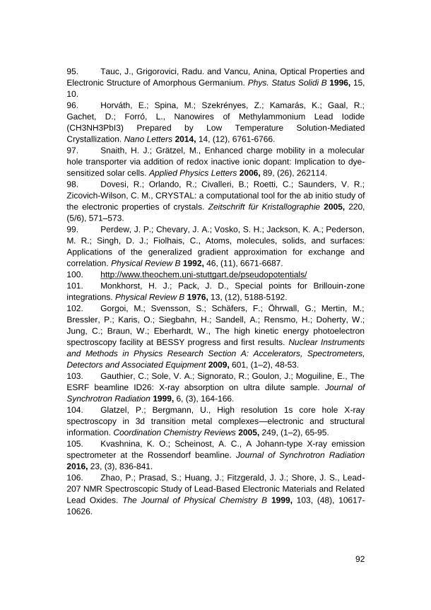
92
95. Tauc, J., Grigorovici, Radu. and Vancu, Anina, Optical Properties and
Electronic Structure of Amorphous Germanium. Phys. Status Solidi B 1996, 15,
10.
96. Horváth, E.; Spina, M.; Szekrényes, Z.; Kamarás, K.; Gaal, R.;
Gachet, D.; Forró, L., Nanowires of Methylammonium Lead Iodide
(CH3NH3PbI3) Prepared by Low Temperature Solution-Mediated
Crystallization. Nano Letters 2014, 14, (12), 6761-6766.
97. Snaith, H. J.; Grätzel, M., Enhanced charge mobility in a molecular
hole transporter via addition of redox inactive ionic dopant: Implication to dye-
sensitized solar cells. Applied Physics Letters 2006, 89, (26), 262114.
98. Dovesi, R.; Orlando, R.; Civalleri, B.; Roetti, C.; Saunders, V. R.;
Zicovich-Wilson, C. M., CRYSTAL: a computational tool for the ab initio study of
the electronic properties of crystals. Zeitschrift für Kristallographie 2005, 220,
(5/6), 571–573.
99. Perdew, J. P.; Chevary, J. A.; Vosko, S. H.; Jackson, K. A.; Pederson,
M. R.; Singh, D. J.; Fiolhais, C., Atoms, molecules, solids, and surfaces:
Applications of the generalized gradient approximation for exchange and
correlation. Physical Review B 1992, 46, (11), 6671-6687.
100. http://www.theochem.uni-stuttgart.de/pseudopotentials/
101. Monkhorst, H. J.; Pack, J. D., Special points for Brillouin-zone
integrations. Physical Review B 1976, 13, (12), 5188-5192.
102. Gorgoi, M.; Svensson, S.; Schäfers, F.; Öhrwall, G.; Mertin, M.;
Bressler, P.; Karis, O.; Siegbahn, H.; Sandell, A.; Rensmo, H.; Doherty, W.;
Jung, C.; Braun, W.; Eberhardt, W., The high kinetic energy photoelectron
spectroscopy facility at BESSY progress and first results. Nuclear Instruments
and Methods in Physics Research Section A: Accelerators, Spectrometers,
Detectors and Associated Equipment 2009, 601, (1–2), 48-53.
103. Gauthier, C.; Sole, V. A.; Signorato, R.; Goulon, J.; Moguiline, E., The
ESRF beamline ID26: X-ray absorption on ultra dilute sample. Journal of
Synchrotron Radiation 1999, 6, (3), 164-166.
104. Glatzel, P.; Bergmann, U., High resolution 1s core hole X-ray
spectroscopy in 3d transition metal complexes—electronic and structural
information. Coordination Chemistry Reviews 2005, 249, (1–2), 65-95.
105. Kvashnina, K. O.; Scheinost, A. C., A Johann-type X-ray emission
spectrometer at the Rossendorf beamline. Journal of Synchrotron Radiation
2016, 23, (3), 836-841.
106. Zhao, P.; Prasad, S.; Huang, J.; Fitzgerald, J. J.; Shore, J. S., Lead-
207 NMR Spectroscopic Study of Lead-Based Electronic Materials and Related
Lead Oxides. The Journal of Physical Chemistry B 1999, 103, (48), 10617-
10626.
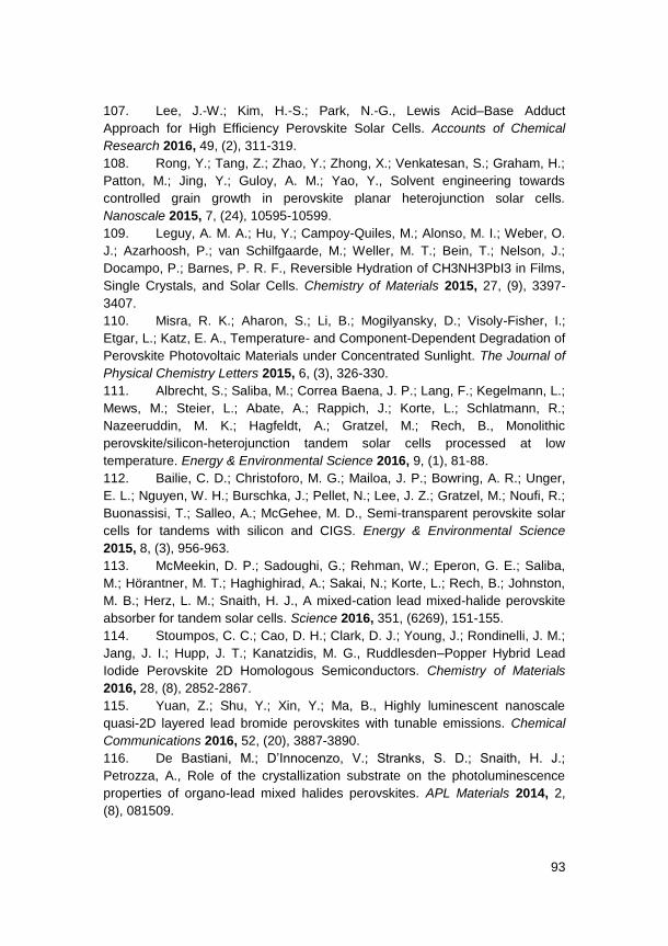
93
107. Lee, J.-W.; Kim, H.-S.; Park, N.-G., Lewis Acid–Base Adduct
Approach for High Efficiency Perovskite Solar Cells. Accounts of Chemical
Research 2016, 49, (2), 311-319.
108. Rong, Y.; Tang, Z.; Zhao, Y.; Zhong, X.; Venkatesan, S.; Graham, H.;
Patton, M.; Jing, Y.; Guloy, A. M.; Yao, Y., Solvent engineering towards
controlled grain growth in perovskite planar heterojunction solar cells.
Nanoscale 2015, 7, (24), 10595-10599.
109. Leguy, A. M. A.; Hu, Y.; Campoy-Quiles, M.; Alonso, M. I.; Weber, O.
J.; Azarhoosh, P.; van Schilfgaarde, M.; Weller, M. T.; Bein, T.; Nelson, J.;
Docampo, P.; Barnes, P. R. F., Reversible Hydration of CH3NH3PbI3 in Films,
Single Crystals, and Solar Cells. Chemistry of Materials 2015, 27, (9), 3397-
3407.
110. Misra, R. K.; Aharon, S.; Li, B.; Mogilyansky, D.; Visoly-Fisher, I.;
Etgar, L.; Katz, E. A., Temperature- and Component-Dependent Degradation of
Perovskite Photovoltaic Materials under Concentrated Sunlight. The Journal of
Physical Chemistry Letters 2015, 6, (3), 326-330.
111. Albrecht, S.; Saliba, M.; Correa Baena, J. P.; Lang, F.; Kegelmann, L.;
Mews, M.; Steier, L.; Abate, A.; Rappich, J.; Korte, L.; Schlatmann, R.;
Nazeeruddin, M. K.; Hagfeldt, A.; Gratzel, M.; Rech, B., Monolithic
perovskite/silicon-heterojunction tandem solar cells processed at low
temperature. Energy & Environmental Science 2016, 9, (1), 81-88.
112. Bailie, C. D.; Christoforo, M. G.; Mailoa, J. P.; Bowring, A. R.; Unger,
E. L.; Nguyen, W. H.; Burschka, J.; Pellet, N.; Lee, J. Z.; Gratzel, M.; Noufi, R.;
Buonassisi, T.; Salleo, A.; McGehee, M. D., Semi-transparent perovskite solar
cells for tandems with silicon and CIGS. Energy & Environmental Science
2015, 8, (3), 956-963.
113. McMeekin, D. P.; Sadoughi, G.; Rehman, W.; Eperon, G. E.; Saliba,
M.; Hörantner, M. T.; Haghighirad, A.; Sakai, N.; Korte, L.; Rech, B.; Johnston,
M. B.; Herz, L. M.; Snaith, H. J., A mixed-cation lead mixed-halide perovskite
absorber for tandem solar cells. Science 2016, 351, (6269), 151-155.
114. Stoumpos, C. C.; Cao, D. H.; Clark, D. J.; Young, J.; Rondinelli, J. M.;
Jang, J. I.; Hupp, J. T.; Kanatzidis, M. G., Ruddlesden–Popper Hybrid Lead
Iodide Perovskite 2D Homologous Semiconductors. Chemistry of Materials
2016, 28, (8), 2852-2867.
115. Yuan, Z.; Shu, Y.; Xin, Y.; Ma, B., Highly luminescent nanoscale
quasi-2D layered lead bromide perovskites with tunable emissions. Chemical
Communications 2016, 52, (20), 3887-3890.
116. De Bastiani, M.; D’Innocenzo, V.; Stranks, S. D.; Snaith, H. J.;
Petrozza, A., Role of the crystallization substrate on the photoluminescence
properties of organo-lead mixed halides perovskites. APL Materials 2014, 2,
(8), 081509.

94
117. Zhang, W.; Saliba, M.; Moore, D. T.; Pathak, S. K.; Hörantner, M. T.;
Stergiopoulos, T.; Stranks, S. D.; Eperon, G. E.; Alexander-Webber, J. A.;
Abate, A.; Sadhanala, A.; Yao, S.; Chen, Y.; Friend, R. H.; Estroff, L. A.;
Wiesner, U.; Snaith, H. J., Ultrasmooth organic–inorganic perovskite thin-film
formation and crystallization for efficient planar heterojunction solar cells. Nat
Commun 2015, 6.
118. Lindblad, R.; Jena, N. K.; Philippe, B.; Oscarsson, J.; Bi, D.; Lindblad,
A.; Mandal, S.; Pal, B.; Sarma, D. D.; Karis, O.; Siegbahn, H.; Johansson, E. M.
J.; Odelius, M.; Rensmo, H., Electronic Structure of CH3NH3PbX3 Perovskites:
Dependence on the Halide Moiety. The Journal of Physical Chemistry C 2015,
119, (4), 1818-1825.
119. Scofield, J., Electron Spectrosc. Relat. Phenom. 1976, 8.
120. Roiland, C.; Trippe-Allard, G.; Jemli, K.; Alonso, B.; Ameline, J.-C.;
Gautier, R.; Bataille, T.; Le Polles, L.; Deleporte, E.; Even, J.; Katan, C.,
Multinuclear NMR as a tool for studying local order and dynamics in
CH3NH3PbX3 (X = Cl, Br, I) hybrid perovskites. Physical Chemistry Chemical
Physics 2016, 18, (39), 27133-27142.
121. Baikie, T.; Barrow, N. S.; Fang, Y.; Keenan, P. J.; Slater, P. R.; Piltz,
R. O.; Gutmann, M.; Mhaisalkar, S. G.; White, T. J., A combined single crystal
neutron/X-ray diffraction and solid-state nuclear magnetic resonance study of
the hybrid perovskites CH3NH3PbX3 (X = I, Br and Cl). Journal of Materials
Chemistry A 2015, 3, (17), 9298-9307.
122. Shmyreva, A. A.; Safdari, M.; Furó, I.; Dvinskikh, S. V., NMR
longitudinal relaxation enhancement in metal halides by heteronuclear
polarization exchange during magic-angle spinning. The Journal of chemical
physics 2016, 144, (22), 224201.
123. Unger, E. L.; Hoke, E. T.; Bailie, C. D.; Nguyen, W. H.; Bowring, A. R.;
Heumuller, T.; Christoforo, M. G.; McGehee, M. D., Hysteresis and transient
behavior in current-voltage measurements of hybrid-perovskite absorber solar
cells. Energy & Environmental Science 2014, 7, (11), 3690-3698.
124. Muljarov, E. A.; Tikhodeev, S. G.; Gippius, N. A.; Ishihara, T., Excitons
in self-organized semiconductor/insulator superlattices: PbI-based perovskite
compounds. Physical Review B 1995, 51, (20), 14370-14378.
125. Loper, P.; Moon, S.-J.; Martin de Nicolas, S.; Niesen, B.; Ledinsky, M.;
Nicolay, S.; Bailat, J.; Yum, J.-H.; De Wolf, S.; Ballif, C., Organic-inorganic
halide perovskite/crystalline silicon four-terminal tandem solar cells. Physical
Chemistry Chemical Physics 2015, 17, (3), 1619-1629.
126. Liu, Y.; Renna, L. A.; Bag, M.; Page, Z. A.; Kim, P.; Choi, J.; Emrick,
T.; Venkataraman, D.; Russell, T. P., High Efficiency Tandem Thin-
Perovskite/Polymer Solar Cells with a Graded Recombination Layer. ACS
Applied Materials & Interfaces 2016, 8, (11), 7070-7076.
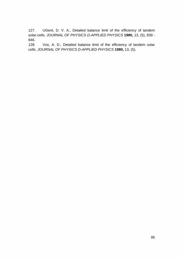
95
127. UGent, D. V. A., Detailed balance limit of the efficiency of tandem
solar-cells. JOURNAL OF PHYSICS D-APPLIED PHYSICS 1980, 13, (5), 839 -
846.
128. Vos, A. D., Detailed balance limit of the efficiency of tandem solar
cells. JOURNAL OF PHYSICS D-APPLIED PHYSICS 1980, 13, (5).


