Datasheet 1 Rev. 1.11www.infineon.com/OPTIREG-Linear 2019-10-21
OPTIREG™ Linear TLE4263-2ES
5 V low drop voltage regulator
Features
• Output voltage tolerance ≤ ±2%
• 180 mA output current capability
• Low-drop voltage
• Very low standby current consumption
• Overtemperature protection
• Reverse polarity protection
• Short-circuit proof
• Adjustable reset threshold
• Watchdog for monitoring microprocessor
• Power-on and undervoltage reset with programmable delay time
• Reset low down to VQ = 1V
• Wide temperature range
• Exposed pad package with excellent thermal behavior
• Suitable for use in automotive electronics
• Green Product (RoHS compliant)
Potential applications
General automotive applications.
Product validation
Qualified for automotive applications. Product validation according to AEC-Q100/101.
Description
The OPTIREG™ Linear TLE4263-2ES is a monolithic integrated very low dropout voltage regulator in a SMD
package PG-DSO-8 exposed pad, especially designed for automotive applications. An input voltage up to 45 Vis regulated to an output voltage of 5.0 V. The component is able to drive loads up to 180 mA. The IC is short-circuit proof by the implemented current limitation and has an integrated overtemperature shutdown.
It additionally provides features like power-on and undervoltage reset with adjustable reset threshold, awatchdog circuit for monitoring a connected microcontroller and an inhibit input for enabling or disabling thecomponent.

Datasheet 2 Rev. 1.11 2019-10-21
OPTIREG™ Linear TLE4263-2ES5 V low drop voltage regulator
The reset output RO is set to “low” in case the output voltage falls below the reset switching threshold VQ,rt.This threshold can be decreased down to 3.5 V by an external resistor divider. The power-on reset delay timecan be programmed by the external delay capacitor CD.
The watchdog circuit provides a monitoring function for microcontrollers: At missing pulses on thewatchdog’s input W the reset output RO is set to “low”. The trigger time for the watchdog pulses can be set bythe external capacitor CD.
The IC can be switched off by the inhibit input, reducing the current consumption to typically 0 mA.
Type Package Marking
TLE4263-2ES PG-DSO-8 exposed pad 4263-2

Datasheet 3 Rev. 1.11 2019-10-21
OPTIREG™ Linear TLE4263-2ES5 V low drop voltage regulator
Features . . . . . . . . . . . . . . . . . . . . . . . . . . . . . . . . . . . . . . . . . . . . . . . . . . . . . . . . . . . . . . . . . . . . . . . . 1
Potential applications . . . . . . . . . . . . . . . . . . . . . . . . . . . . . . . . . . . . . . . . . . . . . . . . . . . . . . . . . . . . . 1
Product validation . . . . . . . . . . . . . . . . . . . . . . . . . . . . . . . . . . . . . . . . . . . . . . . . . . . . . . . . . . . . . . . . 1
Description . . . . . . . . . . . . . . . . . . . . . . . . . . . . . . . . . . . . . . . . . . . . . . . . . . . . . . . . . . . . . . . . . . . . . . 1
Table of contents . . . . . . . . . . . . . . . . . . . . . . . . . . . . . . . . . . . . . . . . . . . . . . . . . . . . . . . . . . . . . . . . . 3
1 Block diagram . . . . . . . . . . . . . . . . . . . . . . . . . . . . . . . . . . . . . . . . . . . . . . . . . . . . . . . . . . . . . . . . . . . 4
2 Pin configuration . . . . . . . . . . . . . . . . . . . . . . . . . . . . . . . . . . . . . . . . . . . . . . . . . . . . . . . . . . . . . . . . . 5
3 General product characteristics . . . . . . . . . . . . . . . . . . . . . . . . . . . . . . . . . . . . . . . . . . . . . . . . . . . . 6
3.1 Absolute maximum ratings . . . . . . . . . . . . . . . . . . . . . . . . . . . . . . . . . . . . . . . . . . . . . . . . . . . . . . . . . . . . . . . . 63.2 Functional range . . . . . . . . . . . . . . . . . . . . . . . . . . . . . . . . . . . . . . . . . . . . . . . . . . . . . . . . . . . . . . . . . . . . . . . . . 73.3 Thermal resistance . . . . . . . . . . . . . . . . . . . . . . . . . . . . . . . . . . . . . . . . . . . . . . . . . . . . . . . . . . . . . . . . . . . . . . . 7
4 Functional description . . . . . . . . . . . . . . . . . . . . . . . . . . . . . . . . . . . . . . . . . . . . . . . . . . . . . . . . . . . . 8
4.1 Choosing external components . . . . . . . . . . . . . . . . . . . . . . . . . . . . . . . . . . . . . . . . . . . . . . . . . . . . . . . . . . . . 8
4.2 Electrical characteristics . . . . . . . . . . . . . . . . . . . . . . . . . . . . . . . . . . . . . . . . . . . . . . . . . . . . . . . . . . . . . . . . . . 84.3 Typical performance characteristics . . . . . . . . . . . . . . . . . . . . . . . . . . . . . . . . . . . . . . . . . . . . . . . . . . . . . . . 10
5 Application information . . . . . . . . . . . . . . . . . . . . . . . . . . . . . . . . . . . . . . . . . . . . . . . . . . . . . . . . . . 14
5.1 Reset . . . . . . . . . . . . . . . . . . . . . . . . . . . . . . . . . . . . . . . . . . . . . . . . . . . . . . . . . . . . . . . . . . . . . . . . . . . . . . . . . . . 155.2 Power-on reset delay time . . . . . . . . . . . . . . . . . . . . . . . . . . . . . . . . . . . . . . . . . . . . . . . . . . . . . . . . . . . . . . . . 15
5.3 Reset adjust function . . . . . . . . . . . . . . . . . . . . . . . . . . . . . . . . . . . . . . . . . . . . . . . . . . . . . . . . . . . . . . . . . . . . 165.4 Watchdog . . . . . . . . . . . . . . . . . . . . . . . . . . . . . . . . . . . . . . . . . . . . . . . . . . . . . . . . . . . . . . . . . . . . . . . . . . . . . . . 16
6 Package information . . . . . . . . . . . . . . . . . . . . . . . . . . . . . . . . . . . . . . . . . . . . . . . . . . . . . . . . . . . . . 18
7 Revision history . . . . . . . . . . . . . . . . . . . . . . . . . . . . . . . . . . . . . . . . . . . . . . . . . . . . . . . . . . . . . . . . . 19
Table of contents
Datasheet 4 Rev. 1.11 2019-10-21
OPTIREG™ Linear TLE4263-2ES5 V low drop voltage regulator
Block diagram
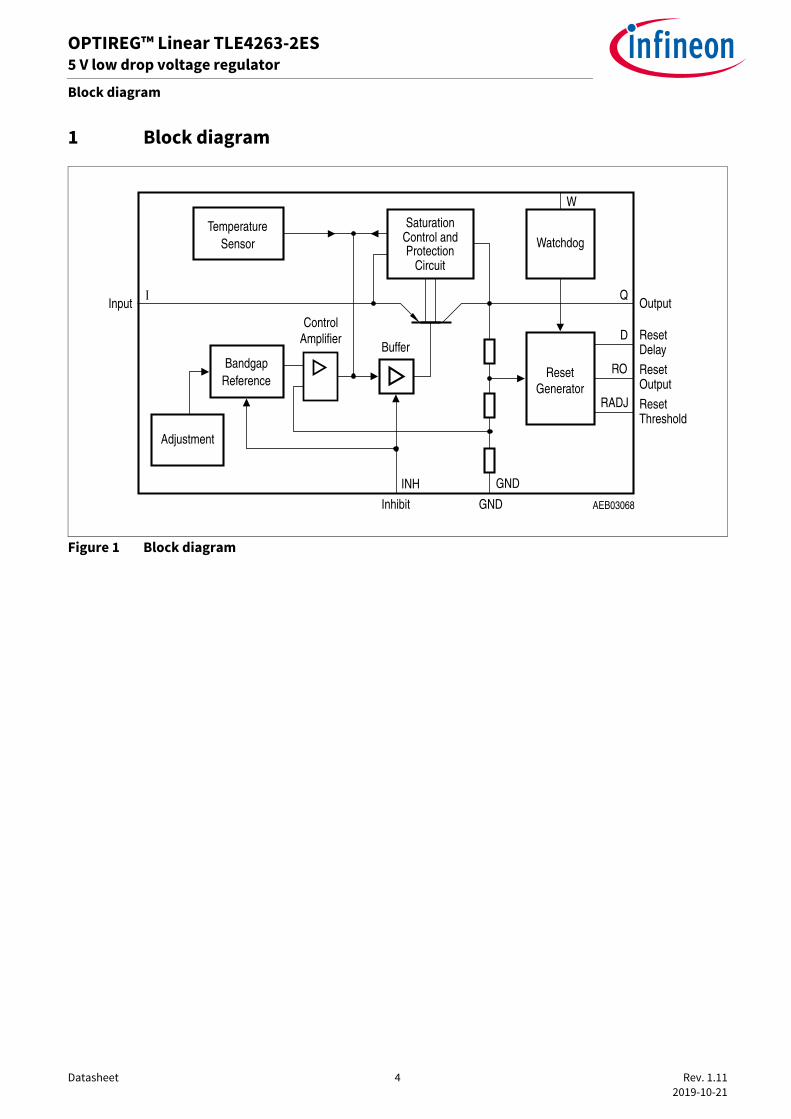
1 Block diagram
Figure 1 Block diagram
Input
AEB03068
INH
GND
Output
D
RO
RADJ
ResetDelay
ResetOutput
ResetThreshold
Watchdog
W
TemperatureSensor
GeneratorReset
ReferenceBandgap
Adjustment
Buffer
ControlAmplifier
SaturationControl andProtection
Circuit
Inhibit
Ι Q
GND
Datasheet 5 Rev. 1.11 2019-10-21
OPTIREG™ Linear TLE4263-2ES5 V low drop voltage regulator
Pin configuration
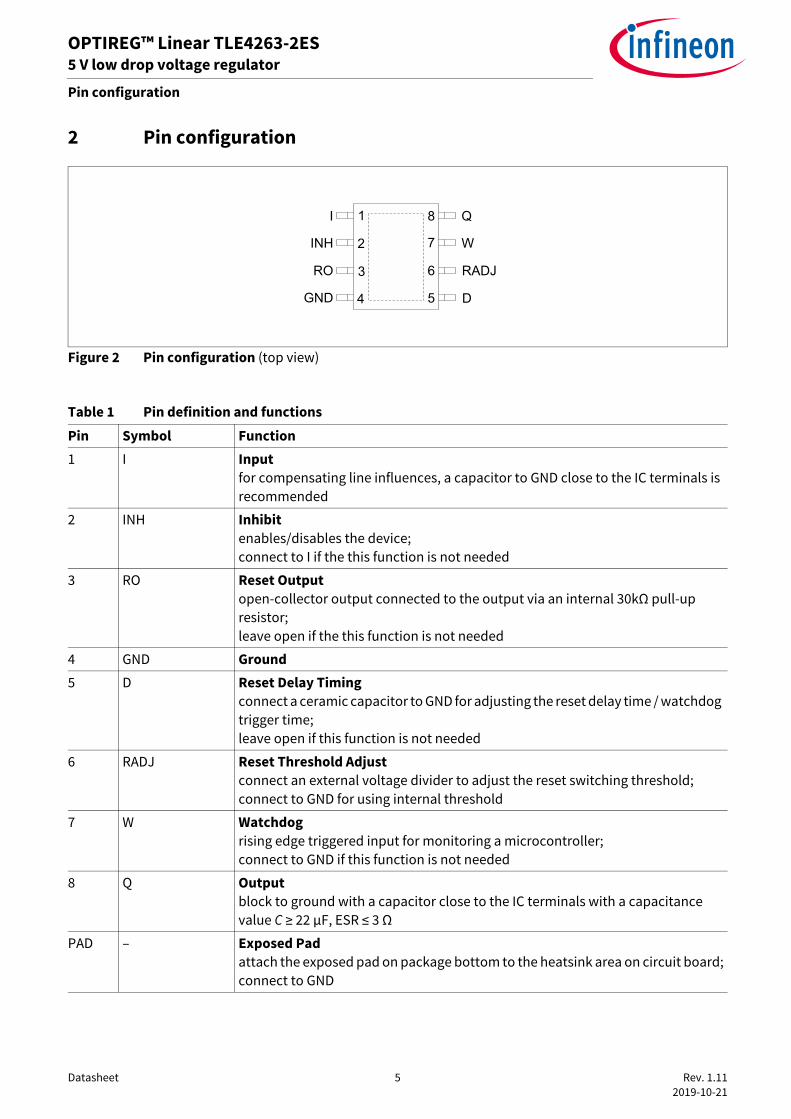
2 Pin configuration
Figure 2 Pin configuration (top view)
Table 1 Pin definition and functions
Pin Symbol Function
1 I Input
for compensating line influences, a capacitor to GND close to the IC terminals is
recommended
2 INH Inhibit
enables/disables the device;connect to I if the this function is not needed
3 RO Reset Output
open-collector output connected to the output via an internal 30kΩ pull-up resistor;
leave open if the this function is not needed
4 GND Ground
5 D Reset Delay Timing
connect a ceramic capacitor to GND for adjusting the reset delay time / watchdog
trigger time;leave open if this function is not needed
6 RADJ Reset Threshold Adjust
connect an external voltage divider to adjust the reset switching threshold;
connect to GND for using internal threshold
7 W Watchdog
rising edge triggered input for monitoring a microcontroller;connect to GND if this function is not needed
8 Q Output
block to ground with a capacitor close to the IC terminals with a capacitance value C ≥ 22 µF, ESR ≤ 3 Ω
PAD – Exposed Pad
attach the exposed pad on package bottom to the heatsink area on circuit board;
connect to GND
1
2
54
3
8
7
6
Q
W
RADJ
D
I
INH
RO
GND

Datasheet 6 Rev. 1.11 2019-10-21
OPTIREG™ Linear TLE4263-2ES5 V low drop voltage regulator
General product characteristics
3 General product characteristics
3.1 Absolute maximum ratings
Table 2 Absolute maximum ratings1)
Tj = -40°C to +150°C; all voltages with respect to ground (unless otherwise specified)
1) Not subject to production test, specified by design.
Parameter Symbol Values Unit Note or
Test Condition
Number
Min. Typ. Max.
Input I
Input voltageInput current
VI
II
- 42–
––
45–
V–
–Internally limited
P_3.1.1
Reset output RO
Input voltageInput current
VRO
IRO
- 0.3–
––
42–
V–
–Internally limited
P_3.1.2
Reset threshold RADJ
Voltage VRADJ - 0.3 – 6 V – P_3.1.3
Reset delay D
VoltageCurrent
VD
ID
- 0.3–
––
42–
V–
–Internally limited
P_3.1.4
Output Q
Voltage
Current
VQ
IQ
0.30
–
–
–
7.0
–
V
–
–
Internally limited
P_3.1.5
Inhibit INH
Input voltageInput current
VINH
IINH
-42–
––
45–
V–
–Internally limited
P_3.1.6
Watchdog W
Voltage VW -0.3 – 6 V – P_3.1.7
Ground GND
Current IGND -0.5 – – A – P_3.1.8
Temperature
Junction temperatureStorage temperature
Tj
Tstg
–-50
––
150150
°C°C
––
P_3.1.9
ESD susceptibility
Human body model (HBM) Voltage – – 2 kV 2)
2) ESD HBM test according JEDEC JESD22-A114
P_3.1.10
Charged device model (CBM) Voltage – – 1 kV 3)
3) ESD CDM test according AEC/ESDA ESD-STM5 3.1-1999
P_3.1.11

Datasheet 7 Rev. 1.11 2019-10-21
OPTIREG™ Linear TLE4263-2ES5 V low drop voltage regulator
General product characteristics
Notes
1. Stresses above the ones listed here may cause permanent damage to the device. Exposure to absolute maximum rating conditions for extended periods may affect device reliability.
2. Integrated protection functions are designed to prevent IC destruction under fault conditions described in the data sheet. Fault conditions are considered as “outside” normal operating range. Protection functions are not designed for continuous repetitive operation.
3.2 Functional range
Note: Within the functional range the IC operates as described in the circuit description. The electrical characteristics are specified within the conditions given in the related electrical characteristics table.
3.3 Thermal resistance
Table 3 Functional range
Parameter Symbol Values Unit Note or Test Condition Number
Min. Typ. Max.
Input voltage VI 5.5 – 45 V 1)
1) Corresponds with characteristics of drop voltage, output current and power description (see diagrams).
P_3.2.1
Junction temperature Tj -40 – 150 °C – P_3.2.2
Table 4 Thermal resistance
Parameter Symbol Values Unit Note or Test Condition Number
Min. Typ. Max.
Junction to case RthJC – 10 – K/W 1) measured to exposed pad
1) Not subject to production test, specified by design
P_3.3.1
Junction to ambient RthJA – 45 – K/W 2)
2) Specified RthJA value is according to Jedec JESD51-2,-5,-7 at natural convection on FR4 2s2p board; The product (Chip+Package) was simulated on a 76.2 × 114.3 × 1.5 mm3 board with 2 inner copper layers (2 × 70 µm Cu, 2 × 35 µm Cu). Where applicable a thermal via array under the exposed pad contacted the first inner copper layer.
P_3.3.2
Junction to ambient RthJA – 153 – K/W footprint only 3)
3) Specified RthJA value is according to Jedec JESD 51-3 at natural convection on FR4 1s0p board; The product (Chip+Package) was simulated on a 76.2 × 114.3 × 1.5 mm3 board with 1 copper layer (1 × 70 µm Cu).
P_3.3.3
Junction to ambient RthJA – 64 – K/W 300 mm2 heatsink area 2) P_3.3.4
Junction to ambient RthJA – 55 – K/W 600 mm2 heatsink area 2) P_3.3.5
Datasheet 8 Rev. 1.11 2019-10-21
OPTIREG™ Linear TLE4263-2ES5 V low drop voltage regulator
Functional description
4 Functional description
The control amplifier compares a reference voltage to a voltage that is proportional to the output voltage anddrives the base of the series transistor via a buffer. Saturation control as a function of the load current prevents
any oversaturation of the power element. The component also has a number of internal circuits for protectionagainst:
• Overload
• Overtemperature
• Reverse polarity
In case the externally scaled down output voltage at the reset adjust input falls below 1.35 V, the external reset
delay capacitor CD is discharged by the reset generator. When the voltage of the capacitor reaches the lowerthreshold VDRL, a reset signal occurs at the reset output and is held until the upper threshold VDU is exceeded.If the reset threshold input is connected to GND, reset is triggered at an output voltage of typically 4.65 V.
4.1 Choosing external components
The input capacitor CI is necessary for compensation of line influences. Using a resistor of approx. 1 Ω in serieswith CI, the oscillating circuit consisting of input inductivity and input capacitance can be damped. The outputcapacitor is necessary for the stability of the regulating circuit. Stability is ensured at values CQ ≥ 22 µF and an
ESR of ≤ 3 Ω within the operating temperature range. For small tolerances of the reset delay the spread of thecapacitance of the delay capacitor and its temperature coefficient should be noted.
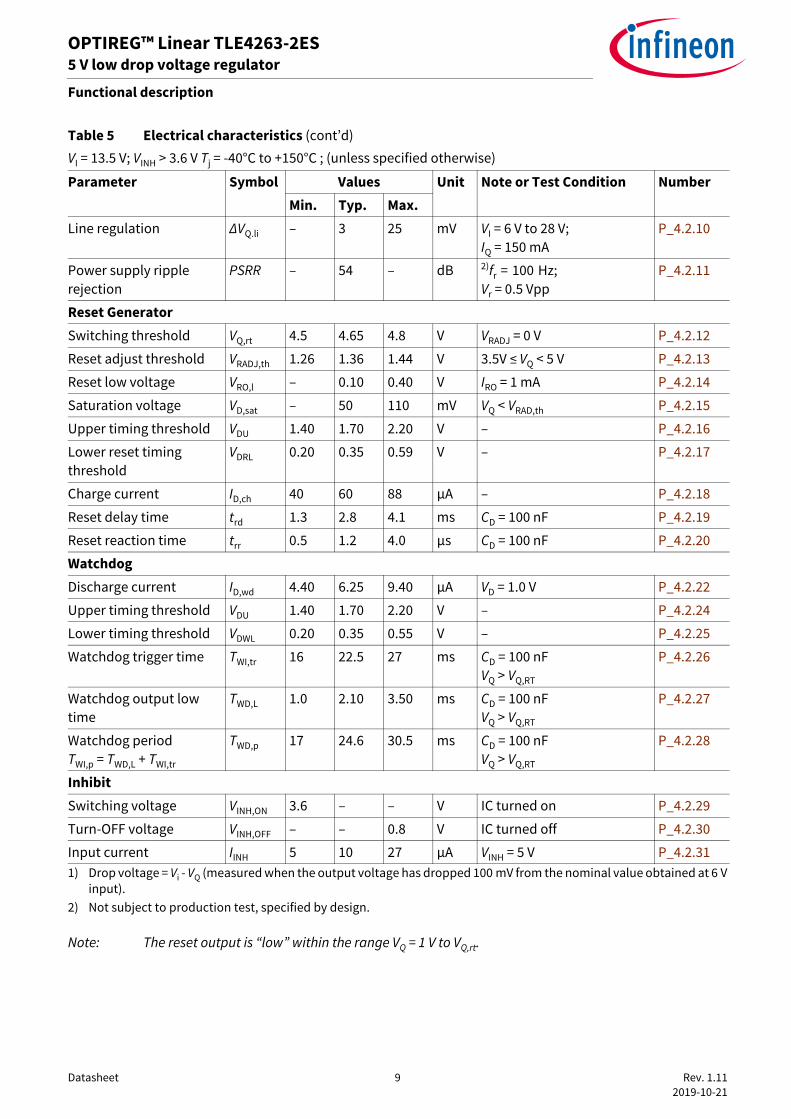
4.2 Electrical characteristics
Table 5 Electrical characteristics
VI = 13.5 V; VINH > 3.6 V Tj = -40°C to +150°C ; (unless specified otherwise)
Parameter Symbol Values Unit Note or Test Condition Number
Min. Typ. Max.
Normal Operation
Output voltage VQ 4.90 5.00 5.10 V 5 mA ≤ IQ ≤ 150 mA;6 V ≤ VI ≤ 28 V
P_4.2.1
Output voltage VQ 4.90 5.00 5.10 V 6 V ≤ VI ≤ 32 V;IQ = 100 mA;
Tj = 100°C
P_4.2.2
Output current limitation IQ,max 180 250 400 mA VQ = 4.8V P_4.2.3
Current consumption;
Iq = II - IQ
Iq – 0 10 µA VINH = 0 V; TJ ≤ 115°C P_4.2.4
Current consumption;
Iq = II - IQ
Iq – 0.90 1.30 mA IQ = 0 mA P_4.2.5
Current consumption;
Iq = II - IQ
Iq – 10 18 mA IQ = 150 mA P_4.2.6
Current consumption;
Iq = II - IQ
Iq – 15 24 mA IQ = 150 mA; VI = 4.5 V P_4.2.7
Dropout voltage Vdr – 0.35 0.50 V IQ = 150 mA 1) P_4.2.8
Load regulation ∆VQ,lo – – 25 mV IQ = 5 mA to 150 mA P_4.2.9
Datasheet 9 Rev. 1.11 2019-10-21
OPTIREG™ Linear TLE4263-2ES5 V low drop voltage regulator
Functional description
Note: The reset output is “low” within the range VQ = 1 V to VQ,rt.
Line regulation ∆VQ.li – 3 25 mV VI = 6 V to 28 V;
IQ = 150 mA
P_4.2.10
Power supply ripple
rejection
PSRR – 54 – dB 2)fr = 100 Hz;
Vr = 0.5 Vpp
P_4.2.11
Reset Generator
Switching threshold VQ,rt 4.5 4.65 4.8 V VRADJ = 0 V P_4.2.12
Reset adjust threshold VRADJ,th 1.26 1.36 1.44 V 3.5V ≤ VQ < 5 V P_4.2.13
Reset low voltage VRO,l – 0.10 0.40 V IRO = 1 mA P_4.2.14
Saturation voltage VD,sat – 50 110 mV VQ < VRAD,th P_4.2.15
Upper timing threshold VDU 1.40 1.70 2.20 V – P_4.2.16
Lower reset timing
threshold
VDRL 0.20 0.35 0.59 V – P_4.2.17
Charge current ID,ch 40 60 88 µA – P_4.2.18
Reset delay time trd 1.3 2.8 4.1 ms CD = 100 nF P_4.2.19
Reset reaction time trr 0.5 1.2 4.0 µs CD = 100 nF P_4.2.20
Watchdog
Discharge current ID,wd 4.40 6.25 9.40 µA VD = 1.0 V P_4.2.22
Upper timing threshold VDU 1.40 1.70 2.20 V – P_4.2.24
Lower timing threshold VDWL 0.20 0.35 0.55 V – P_4.2.25
Watchdog trigger time TWI,tr 16 22.5 27 ms CD = 100 nFVQ > VQ,RT
P_4.2.26
Watchdog output low time
TWD,L 1.0 2.10 3.50 ms CD = 100 nFVQ > VQ,RT
P_4.2.27
Watchdog periodTWI,p = TWD,L + TWI,tr
TWD,p 17 24.6 30.5 ms CD = 100 nFVQ > VQ,RT
P_4.2.28
Inhibit
Switching voltage VINH,ON 3.6 – – V IC turned on P_4.2.29
Turn-OFF voltage VINH,OFF – – 0.8 V IC turned off P_4.2.30
Input current IINH 5 10 27 µA VINH = 5 V P_4.2.31
1) Drop voltage = Vi - VQ (measured when the output voltage has dropped 100 mV from the nominal value obtained at 6 V input).
2) Not subject to production test, specified by design.
Table 5 Electrical characteristics (cont’d)
VI = 13.5 V; VINH > 3.6 V Tj = -40°C to +150°C ; (unless specified otherwise)
Parameter Symbol Values Unit Note or Test Condition Number
Min. Typ. Max.
Datasheet 10 Rev. 1.11 2019-10-21
OPTIREG™ Linear TLE4263-2ES5 V low drop voltage regulator
Functional description
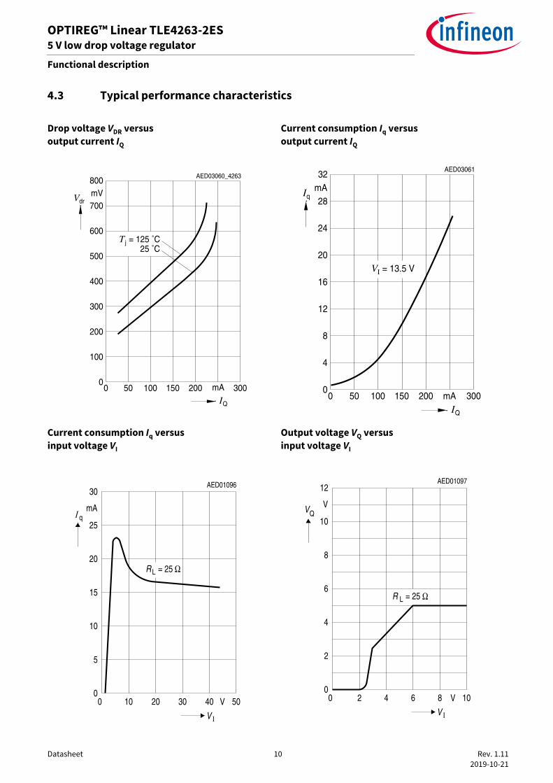
4.3 Typical performance characteristics
Drop voltage VDR versus
output current IQ
Current consumption Iq versus
output current IQ
Current consumption Iq versus
input voltage VI
Output voltage VQ versus
input voltage VI
AED03060_4263
00
QI50 100 150 200 300mA
100
200
300
400
500
600
700
800mVVdr
jT = 125 ˚C25 ˚C
AED03061
00
QI
qI
50 100 150 200 300
IV = 13.5 V
mA
4
8
12
16
20
24
28
32mA
15
10
5
200 100
20
mA
30
25qΙ
= 25R L
50V30 40
V Ι
AED01096
Ω
R6
4
2
040 2
8
12
10QV V
10V6 8
V Ι
AED01097
= 25L Ω

Datasheet 11 Rev. 1.11 2019-10-21
OPTIREG™ Linear TLE4263-2ES5 V low drop voltage regulator
Functional description
Output current IQ versus
input voltage VI
Timing threshold voltage VDU and VDRL versus
junction temperature TJ
Reset switching threshold VRADJ versus
junction temperature TJ
Current consumption of inhibit IINH versus
junction temperature TJ
T
1000
50
100
20
250
300
QΙmA
200
150
V
4030 V
Ι
50
= 25 Cj
AED01091 AED03062
-400
IV = 13.5 V
0.4
0.8
1.2
1.6
2.0
2.4
2.8
3.2V
0 40 80 120 160˚C
V
T j
VDRL
DUV
AED01088
-40 0 40 80 120 ˚C 1600
jT
RADJV
0.2
0.4
0.6
0.8
1.0
1.2
1.4
1.6V
AED03063
VINH = 5 V
µAINHI
80-40
4
2
0
6
8
400
10
12
14
16
160˚C120T j

Datasheet 12 Rev. 1.11 2019-10-21
OPTIREG™ Linear TLE4263-2ES5 V low drop voltage regulator
Functional description
Charge current and discharge current ID,ch ; ID,dis
versus junction temperature TJ
Output voltage VQ versus
junction temperature TJ
40
20
30
10
0-40 400
80
60
70
50
ΙA
C12080 160
T j
AED03064
μ
= 13.5 V= 1.5 V
ΙVV D
Ι D, ch
D, disΙ
AED01090
-40 0 40 80 120 ˚C 1604.6
jT
QV
VI = 13.5 V
4.7
4.8
4.9
5.0
5.1
V5.2

Datasheet 13 Rev. 1.11 2019-10-21
OPTIREG™ Linear TLE4263-2ES5 V low drop voltage regulator
Functional description
Undervoltage reset adjust threshold VRADJ versus
output voltage VQ
Pulse time TWI,tr versus
junction temperature TJ
Power supply ripple rejection PSRR versus
ripple frequency fr
Output capacitor series resistor ESR CQ versus
output current IQ
0.8
0.4
0.6
0.2
10 20
1.6
1.2
1.4
1.0
RADJV V
V43 5
V Q
AED01098_4263
ΙV = 13.5 V20
10
15
5
0-40 400
40
30
35
25
WI,trT
C12080 160
T j
AED03065_4263
ms
V Ι = 13.5 V= 100 nFCD
10f [Hz]
10k
PSRR[dB]
1_PSRR_F.SVG
60
50
100 1k 100k
80
30
40
Vripple = 1 VVI = 13.5 VCQ = 22 μF tantalumTj = 25 °C
IQ = 1 mAIQ = 10 mAIQ = 100 mA
2_ESR-IQ.VSD
1
0.1
0.01
ESRCQ[Ω]
0IQ [mA]
100
100
10
StableRegion
50 150
CQ = 22 µFTj = -40...150 °C

Datasheet 14 Rev. 1.11 2019-10-21
OPTIREG™ Linear TLE4263-2ES5 V low drop voltage regulator
Application information
5 Application information
Note: The following information is given as a hint for the implementation of the device only and shall not be regarded as a description or warranty of a certain functionality condition or quality of the device.
Figure 3 Application circuit
Note: This is a very simplified example of an application circuit. The function must be verified in the real application.
AES03070_4263
22 F
ΙQ
ΙRD
VRADJ
Ω5.6 k
D
ROINHEΙ
1000 F 470 nF
Ι Ι
VE DCVC
GNDΙD, chΙVRO
QVVΙ
TLE4263-2 ESμ μ
GND
WV
W RADJ
100 nF
Ι Q
Vr+
PSRR = 20 logVr
Q, rVΔ

Datasheet 15 Rev. 1.11 2019-10-21
OPTIREG™ Linear TLE4263-2ES5 V low drop voltage regulator
Application information
5.1 Reset
Figure 4 Reset timing diagram
5.2 Power-on reset delay time
If the application needs a power-on reset delay time trd different from the value given in “Reset Generator”
on Page 9, the delay capacitor’s value can be derived from these specified values and the desired power-ondelay time:
(5.1)
with:
• CD: capacitance of the delay capacitor to be chosen
• trd,new: desired power-on reset delay time
• trd: power-on reset delay time specified in this datasheet
For a precise calculation also take the delay capacitor’s tolerance into consideration.
VI
t
VQ
t
VQ,rt
VRO
TimingDiagram_Reset.vsd
tVRO,l
1 V
1V
trd
ThermalShutdown
InputVoltage Dip
trrtrd trd
t < trr
trd
Under-voltage
Spike atoutput
Over-load
VDRL
VDU
t
VD

Datasheet 16 Rev. 1.11 2019-10-21
OPTIREG™ Linear TLE4263-2ES5 V low drop voltage regulator
Application information
5.3 Reset adjust function
The undervoltage reset switching threshold can be adjusted according to the application’s needs byconnecting an external voltage divider (RADJ1, RADJ2) at pin RADJ. For selecting the default threshold connect
pin RADJ to GND.
When dimensioning the voltage divider, take into consideration that there will be an additional currentconstantly flowing through the resistors.
With a voltage divider connected, the reset switching threshold VRT,new is calculated as follows:
(5.2)
with
• VRT,new: the desired new reset switching threshold
• RADJ1, RADJ2: resistors of the external voltage divider
• VRADJ,th: reset adjust switching threshold given in “Reset Generator” on Page 9
5.4 Watchdog
Figure 5 Timing of the watchdog function reset
VRT new,
RADJ 1, R+ ADJ 2,RADJ 2,
------------------------------------------ VRADJ th,×=
VW
t
VRO
TimingDiagram_Watchdog.vsd
tVRO,l
TWD,L
TWI,tr
VDWL
VDU
t
VD
TWD,L
TWI,p
No positive VW edge

Datasheet 17 Rev. 1.11 2019-10-21
OPTIREG™ Linear TLE4263-2ES5 V low drop voltage regulator
Application information
Watchdog timing
The period of the watchdog pulses has to be smaller than the minimum watchdog trigger time which is set bythe external reset delay capacitor CD. Use the following formula for dimensioning CD:
(5.3)
with
• CD: capacitance of the delay capacitor to be chosen
• TWI,tr,new: desired watchdog trigger time
• TWI,tr: watchdog trigger time specified in this data sheet
CDTWI,tr,new
TWI,tr------------------------ 100 nF×=

Datasheet 18 Rev. 1.11 2019-10-21
OPTIREG™ Linear TLE4263-2ES5 V low drop voltage regulator
Package information
6 Package information
Figure 6 PG-DSO-8 exposed pad (Plastic Dual Small Outline)1)
Green Product (RoHS compliant)
To meet the world-wide customer requirements for environmentally friendly products and to be compliantwith government regulations the device is available as a green product. Green products are RoHS-Compliant(i.e Pb-free finish on leads and suitable for Pb-free soldering according to IPC/JEDEC J-STD-020).
Further information on packages
https://www.infineon.com/packages
1) Dimension in mm
GPS05094
PG-DSO-8-27-PO V01
1 4
8 5
8
1 4
5
8x0.41±0.09 2)
M0.2 DC A-B
1.27C
Sta
nd O
ff
+0 -0.1
0.1
(1.4
5)
1.7
MA
X.
0.08Seating Plane
C
A
B
4.9±0.11)A-BC0.1 2x
3) JEDEC reference MS-012 variation BA
1) Does not include plastic or metal protrusion of 0.15 max. per side 2) Dambar protrusion shall be maximum 0.1 mm total in excess of lead width
Bottom View
±0.23
±0.2
2.65
0.2±0.2D
6 M D 8x
0.64±0.25
3.9±0.11)0.1
0.35 x 45˚
C D 2x
+0.0
60.
19
8˚ M
AX
.
Index Marking
Datasheet 19 Rev. 1.11 2019-10-21
OPTIREG™ Linear TLE4263-2ES5 V low drop voltage regulator
Revision history
7 Revision history
Revision Date Changes
1.11 2019-10-21 Editorial changes
1.1 2019-03-27 Updated layout and structure
Editorial changes
1.0 2008-04-21 Initial datasheet

Trademarks
All referenced product or service names and trademarks are the property of their respective owners.
Edition 2019-10-21
Published by
Infineon Technologies AG
81726 Munich, Germany
© 2007 Infineon Technologies AG.
All Rights Reserved.
Do you have a question about any aspect of this document?
Email: [email protected]
Document referenceZ8F52231382
IMPORTANT NOTICE
The information given in this document shall in noevent be regarded as a guarantee of conditions orcharacteristics ("Beschaffenheitsgarantie"). With respect to any examples, hints or any typicalvalues stated herein and/or any information regardingthe application of the product, Infineon Technologieshereby disclaims any and all warranties and liabilitiesof any kind, including without limitation warranties ofnon-infringement of intellectual property rights of anythird party. In addition, any information given in this document issubject to customer's compliance with its obligationsstated in this document and any applicable legalrequirements, norms and standards concerningcustomer's products and any use of the product ofInfineon Technologies in customer's applications. The data contained in this document is exclusivelyintended for technically trained staff. It is theresponsibility of customer's technical departments toevaluate the suitability of the product for the intendedapplication and the completeness of the productinformation given in this document with respect tosuch application.
For further information on technology, delivery termsand conditions and prices, please contact the nearestInfineon Technologies Office (www.infineon.com).
WARNINGS
Due to technical requirements products may containdangerous substances. For information on the typesin question please contact your nearest InfineonTechnologies office.
Except as otherwise explicitly approved by InfineonTechnologies in a written document signed byauthorized representatives of Infineon Technologies,Infineon Technologies’ products may not be used inany applications where a failure of the product or anyconsequences of the use thereof can reasonably beexpected to result in personal injury.


