
NATIONAL RADIO ASTRONOMY OBSERVATORY
CHARLOTTESVILLE, VIRGINIA
ELECTRONICS DIVISION INTERNAL REPORT No. 187
THE NRAO VLBI MARK II PROCESSOR
B. MEREDITH AND B. RAYHRER
JUNE 1978
NUMBER OF COPIES: 150
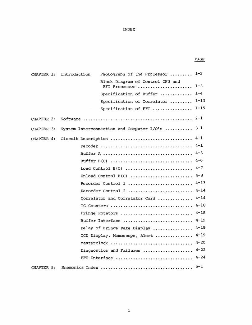
INDEX
PAGE
CHAPTER 1: Introduction Photograph of the Processor ............... 1-2
Block Diagram of Control CPU andFFT Processor ....................................... 1-3
Specification of Buffer ...................... 1-4
Specification of Correlator ............... 1-13
Specification of FFT ............................ 1-15
CHAPTER 2: Software ................................................................................ 2-1
CHAPTER 3: System Interconnection and Computer I/o's ................... 3-1
CHAPTER 4: Circuit Description ........................................................... 4-1
Decoder ................................................................... 4-1
Buffer A ................................................................. 4-3
Buffer B(C) ........................................................... 4-6
Load Control B(C) ................................................ 4-7
Unload Control B(C) ............................................. 4-8
Recorder Control 1 .............................................. 4-13
Recorder Control 2 .............................................. 4-14
Correlator and Correlator Card ........................ 4-14
TC Counters ........................................................... 4-18
Fringe Rotators .................................................... 4-18
Buffer Interface .................................................. 4-19
Delay of Fringe Rate Display ............................ 4-19
TCD Display, Memoscope, Alert .......................... 4-19
Masterclock ........................................................... 4-20
Diagnostics and Failures ................................... 4-22
FFT Interface ........................................................ 4-24
CHAPTER 5: Mnemonics Index ................................................................... 5-1
THE NRAO VLBI MARK II PROCESSOR
CHAPTER 1: Introduction
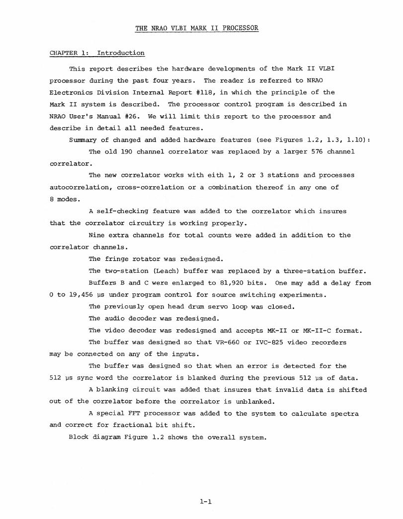
This report describes the hardware developments of the Mark II VLBIprocessor during the past four years. The reader is referred to NRAO
Electronics Division Internal Report #118, in which the principle of theMark II system is described. The processor control program is described in
NRAO User's Manual #26. We will limit this report to the processor anddescribe in detail all needed features.
Summary of changed and added hardware features (see Figures 1.2, 1.3, 1.10):The old 190 channel correlator was replaced by a larger 576 channel
correlator.
The new correlator works with eith 1, 2 or 3 stations and processes
autocorrelation, cross-correlation or a combination thereof in any one of8 modes.
A self-checking feature was added to the correlator which insures
that the correlator circuitry is working properly.
Nine extra channels for total counts were added in addition to the
correlator dhannels.The fringe rotator was redesigned.
The two-station (Leach) buffer was replaced by a three-station buffer.
Buffers B and C were enlarged to 81,920 bits. One may add a delay from
0 to 19,456 Ps under program control for source switching experiments.The previously open head drum servo loop was closed.
The audio decoder was redesigned.
The video decoder was redesigned and accepts MK-II or MK-II-C format.
The buffer was designed so that VR-660 or IVC-825 video recordersmay be connected on any of the inputs.
The buffer was designed so that when an error is detected for the512 ps sync word the correlator is blanked during the previous 512 ps of data.
A blanking circuit was added that insures that invalid data is shiftedout of the correlator before the correlator is unblanked.
A special FFT processor was added to the system to calculate spectraand correct for fractional bit shift.
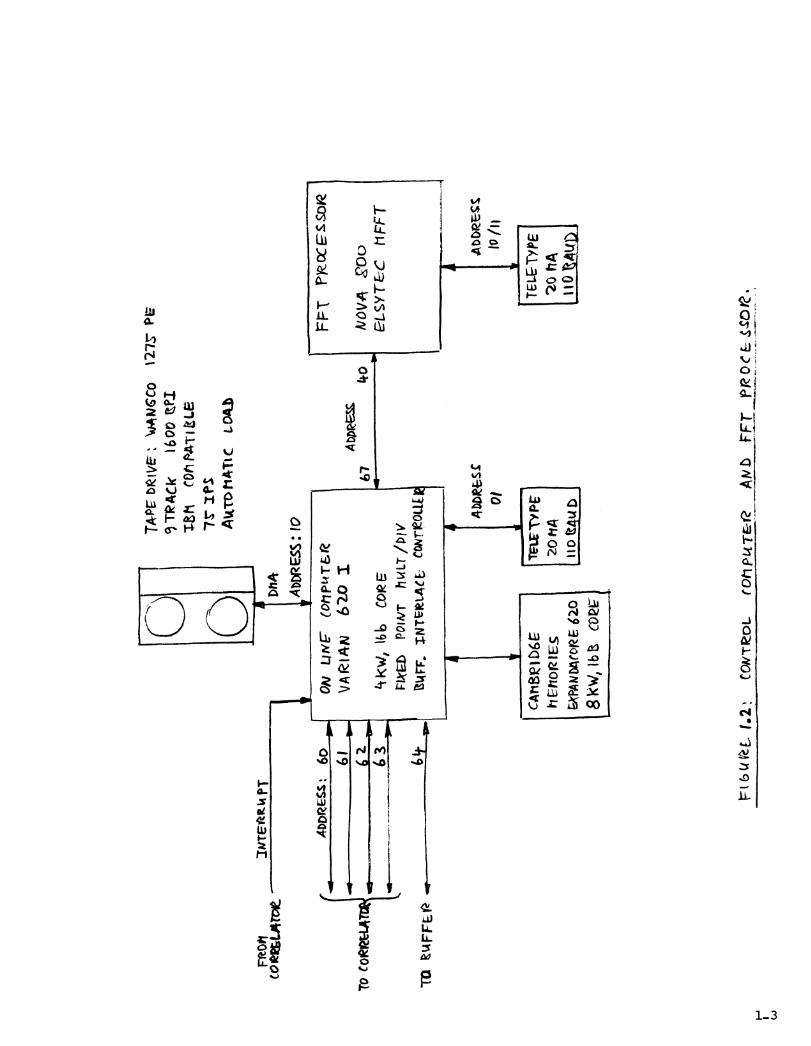
Block diagram Figure 1.2 shows the overall system.

•1111 ••• N
IS
S
IN
lea
rit#
Sap
Iiitle.W
atit*
t..
:t)
Ep a;
..........
>5"
•
rto
to
witid
fn
eM
atrrg
irr,7
7.• 1
1"'
ON
MIR
SIN
V
„,
MO
O:,
„
P/1
(:) to
g
rap
h
••
••• • •
• •
••
•*•
••
•• •
••••
••••
• ,•
••;.
••
•
ON
Uw
e o
tipte
r&R
VA
kti
ktv
62
0
4kW
, lb
CoP
Eri
x m P
OIA
/T h
l4L
T /
NV
tt4rF
, T
NT
it zt
rike
E, C
oN
rieO
LIE
Dpe
Sst
41)D
kEst
AD
DR
E-s
t
ID /i
s
cAtiB
RID
‘EhE
rfo
rzlE
s
WcP
AN
DIv
oR
E 6
208
kW
ilb
Ct 0
P6-
-
TE
LE
TY
PE20 tt
4It
o 1
14141)
A-D
DR
Ess
: 6o
61
TO
coR
MLA
-
ttA
FF
E0
CO
*M
OM
*.
Fre
pti
D/T
Eif
kit
k 4 P
T
DhAr
AD
DR
ESS:
10Tk
PE
bR
iVE
\AA
NG
to 1
27.7
TR
Ack 1
600 t
tP1
TE
N r
OtIP
AT
I aLE
Ir I
PS
taro
MA
TI L
okb
67
-t(D
uro.
, 1.1
! C
OA
rreoL
(oh P
wre
a A
PI)
rF
r prz
ocE
sto
te.
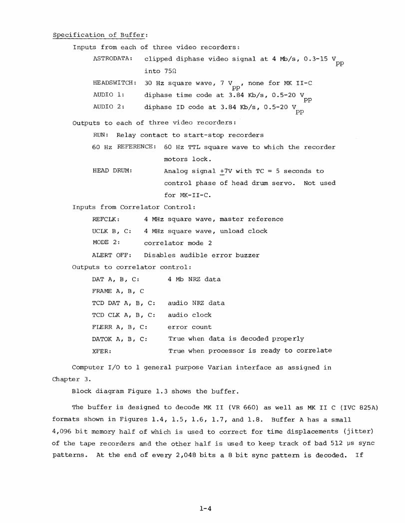
Specification of Buffer:
Inputs from each of three video recorders:
ASTRODATA: clipped diphase video signal at 4 Mb/s, 0.3-15 VPP
into 752
HEADSWITCH: 30 Hz square wave, 7 V , none for MK II-CPP
AUDIO 1: diphase time code at 3.84 Kb/s, 0.5-20 VPP
AUDIO 2: diphase ID code at 3.84 Kb/s, 0.5-20 VPP
Outputs to each of three video recorders:
RUN: Relay contact to start-stop recorders
60 Hz REFERENCE: 60 Hz TTL square wave to which the recorder
motors lock.
HEAD DRUM: Analog signal +7V with TC = 5 seconds to
control phase of head drum servo. Not used
for MK-II-C.
Inputs from Correlator Control:
REFCLK: 4 MHz square wave, master reference
UCLK B, C: 4 MHz square wave, unload clockMODE 2: correlator mode 2
ALERT OFF: Disables audible error buzzer
Outputs to correlator control:
DAT A, B, C: 4 Mb NRZ data
FRAME A, B, C
TCD DAT A, B, C: audio NRZ data
TCD CLK A, B, C: audio clock
FLERR A, B, C: error count
DATOK A, B, C: True when data is decoded properly
XFER: True when processor is ready to correlate
Computer I/O to 1 general purpose Varian interface as assigned in
Chapter 3.
Block diagram Figure 1.3 shows the buffer.
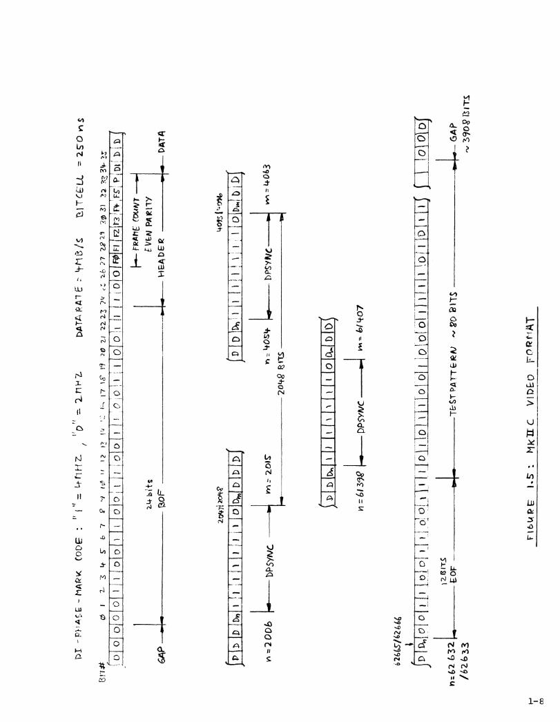
The buffer is designed to decode MK II (VR 660) as well as MK II C (IVC 825A)
formats shown in Figures 1.4, 1.5, 1.6, 1.7, and 1.8. Buffer A has a small
4,096 bit memory half of which is used to correct for time displacements (jitter)
of the tape recorders and the other half is used to keep track of bad 512 Ps sync
patterns. At the end of every 2,048 bits a 8 bit sync pattern is decoded. If
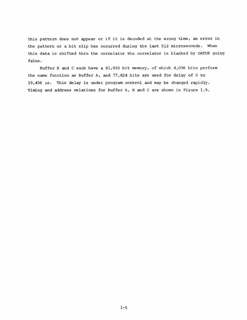
this pattern does not appear or if it is decoded at the wrong time, an error inthe pattern or a bit slip has occurred during the last 512 microseconds. Whenthis data is shifted thru the correlator the correlator is blanked by DATOK goingfalse.
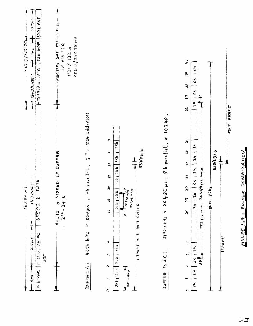
Buffer B and C each have a 81,920 bit memory, of which 4,096 bits performthe same function as Buffer A, and 77,824 bits are used for delay of 0 to
19,456 ps. This delay is under program control and may be changed rapidly.
Timing and address relations for Buffer A, B and C are shown in Figure 1.9.

13, S
Ywc
tiEtt
DA
TA
A 8
C.,
To
ST
AR
T/
101
A/c
F L
AI
licL
ICA
L
rRA
ttE
CT
To
6'2
0 I
T
I to tt
, SY
NC
tt&
tle
LO
po tot R
14 :
D er, R
.oi
tt
a
DD
R
UN
LO
A
SyN
t bt7
r:cr
%1
POIN
TER
Fio
Not
.TD
r6 1
E 1
4
1)4
77rA
MIA
0-
■•••
•
AV
D10
T A-(
00
V
Ec O
DE
v? ?U.
6f3
o
60H
z B
vcr
Dlo
AU
DID
Z
AS
TR
O C
beA
,
tDF
SYK t
)flC
T
ottt
. Pou
ltr02
-
/tom
sYN
C tiE
ti
AD
DR
urF
Elt
B t
it W
t..0
0t
D
at-
DA
TA
C
CO
)2)2
_ EL
K
Lk C
U<
Cti
NO
ST(>
12E
7if
tOk
keelT
81
3P
ock-
t[—
DAT
A
LL 0
DE
LA
', 0
-19,
4-t- s- P
iss s
TE
p
Pot-
i 0_0
Tcp
DA
TA
8
CO
RR
%L
t(
tc c
r.*
TRor
i bitois
l
k AN
t_04 D
tott
ri-P
.0„
DE
LA
Y D
IG ) 1Lt
hS
SS
S S
TE
P
"Teo
m
borizc
AuD
iog
RD10
2.
/ it t/
L0A
C c
Pi
Ci L
.a0
ti 62
0 z
Ait
ipto
x D
E.,(
rDt- _
AbD
k
DATA
DA
TA
A
cOgyZ
BL
ic
RE
F C
-1-k
Po
ire
rErt
60H
2 A
A( P
op A
dt,
c
Atk
DO
I
Alg
al Z
L-0
4D P
oi N
T&
R 10
13
Sytic D
urE
CT
-.D
AT
A
t)6-C
0E)
Elz
.ru
iz66o/2
zs•
),,, 4 Dlo
1)6
( OD

lis--F
RA
IIE
Cot
tivr
evet
v PA
RIT
Y
HE
AD
ER
DAT
AG
AP
ITS
OF
DI
-PH
AS
E -
frA
PV
CO
DE "
1"
t it 1H
Z.it
iNZ
DA
TA R
ATE
- =C
ELL
aS
1) s
1T#
0
1 2.
zs-
26 2
7 1
2 2
9 'V
31
al 3
3 3
4. r
Sititi
2/3
(L
oci<
Z
.b6 M
HZ
_(
o to I
F01
9 IF
2.1F
3IFO
rg(
P D
I)D
20
14
71
10
4V
409S
- 4-0
91,
fD11
) Zoo‘
1)1
111
11
1111
E110
111.,
...t
.
DP
SYN
Chi-
2o1
g"
D D
Dh)
I 1
D,I
D4
i i-D
Et t
Sy1
vC_
dit
00
2.(7
44 B
ITS
Df
é0
23
6 6
02
.tf
izai
rs6 6
, 000
4.I“
o0/
-16
—G
4P
#v 4
2 f
t IT
Sl'
-t-PA
TT
ER
A)
SO
err
rt6
t4ree t
el +
t M
K J
E \
flo
e() T
OR
mic
r,
0 i I
' I, I 0
10
FO
0 I
ri F
2 r3
, pi-
P D
I! I
)0
D0
zote
i zo
ltg'
Lko?
51P,
DIC
,
r-P
AriE
cot
wi
V6N
PA
iet-T
YH
EA
DE
R■
DATA
0=2006
lowat m
tf r1 z
- 2017
VI
— 1 +O
st i-
20
4-R
Bits
11.
GAP
DPS
YN
C-
bPSY
Nc.
:_-- 4
-063
m =
6133
9 D
PSY
/vC
V1
i- 6
/ L
t07
1- 1°1
1TO
TI T)
1010
I 101
0101
W;
TE
ST
Pti I
TE
PA
)PC
)G
AP
390P
13
its
6266
5162
664
iDE
DO
1O
1t it
I-010111i' 0
1i0
11
11
:62
632
/62.
633
izerr
sor
•
-PP
AC„6
-M
AR
( C
OD
e'1
= L
trif
f Z
.t'0
" --
--ri
H 2
.r)
Ait
, PA
1 E
4i/
ITCEL
L25
-0 n
s
Bri
st0 1
2 - 3 4
- s-
b 7
g i
ev)
1�It
t17
t9 2
o 2
_1 2
213 ?
t i?,
t, 27
'a2'
P)
"30
3)
V-16
1412
i.5
liK
IL c
VID
E° r
nRVIA
T

111111111111
11111111110 El
NMF 5 El
Elnifill1
2111121
MEMJ
Milt
1)1
SYM
BO
L W
EI
GiffiN
G
FU
NCTIO
N
• Fo
2
0FR
AM
E C
0UN
T(0
-59)
1F
1
FRAM
E C
OU
NT(0
-59)
SECO
ND
S (U
NIT
S)
SECO
ND
S (U
NIT
S)
SECO
ND
S (T
ENS)
SECO
ND
S (T
ENS)
F2
F 3 F 4 F5 100
S01
SO2
S O3 10
Si,
S1
2
S1
3
2
2
23 2
4
250 0
10 , 0
10 ,21
100,2
21 0
0.2
3
10
1 ,2
0
11 0
,21
1 01
,22
1 01.
23
010
,2
3 DAYS
I10
,2
0 DAYS
I10 ,2I
101,2
210
1
,23
102,2
0
102
,2/
10
2,
2 2
(UN
ITS)
(TE
NS
)
(TE
NS
)
(HU
ND
RE
DS)
(HU
ND
RE
DS)
DA
YS
DA
YS
DA
YS
DRA
WN
•CH
ECK
EDD
ESIG
NEN
GIN
EER
PRO
JEC
TR
EL
EA
SE
DES
IGN
APP
RO
VA
L
••
,,L u
s O
THER
WIS
E SP
ECIF
IE9
MIS
SIO
NS A
RE IN
INCP
W
TOLE
RAN
CES
2.
•to
wIS
A "
!41
04
" IN
PU
T T
I' R
EC
OR
D E
NC
OD
ER
.
1. •
mat
1.•
'1q
4"
11, Pum
p F
rico
PE
R.
NO
MEN
CLA
TUR
E O
R D
ESC
RIP
TIO
N
SIZE
COD
E 1D
ENT
NO
.I
B 9
6 2
61
RE
VIS
IO
NS
DE
SC
RIP
TIO
ND
AT
E
OLD
FO
RN
4T A
VD
10 'TRACK I
I
FIG
UR
E 1
4
Offi
leill
iffin
iffla
idM
irri
nial
litad
nille
ille
fa
LEG
END
SYM
BOL
_JO
LETTiN
GfU
NCTIQ
RH
12
1 0 ,2
HO
URS
(TEN
S)H
13 00
00
1 02 03 10D
II
01
2
013
0 20
02
1
022
I3
10,2
HO
URS
(TEN
S)0
1 0 ,
20 DAYS (
UN
ITS)
10
0,2
10
10 ,
22
SY
MB
OL
1,(
LIG
HT
ING
DA
YS
(H
UN
DR
ED
S)
AU
XIL
IAR
Y I
NP
UT
S
xx
Pt S
IGN
APP
RO
VA
t.
FIN
IStf
•
oT
vey
P41
11 A
r,Sv
usm
No•
NA
;to 0
APP
i ICA
TIO
NCi
.NFR
(.1
4Nt
4T
3
•••
••••••••■
•• •
• •
•■
••■
•••■
■•••.1
11..
..
SYM
BO
L
MOO
MO
IH 0
2
m 03
H 10
H 11
141
2
H 13
00
H01
MO
2
03 /410
HI 1
5.
AL
L I
NP
UT
S A
RE
DA
TA
.14
,I B
IT I
S "
I" F
OR
FR
AM
E I
FN
OH
Or
66.0
01
AN
D "
Or
FO
R 6
6.0
00
.3. ALL
EXTERN
AL
INPU
TS M
US
T B
E I
N T
HE
BC
D F
OR
MA
T
? L'
•
WE
IGH
TIN
G
10
0,2
0
10
0,2
I
100
,22
1 00
,23
10
1,2
0
10
1,2
I
101
,22
101
,23
10
0,2
0
10
0,
2
1
0 2
10 ,2
100
,23
110
,20
110
.2
1
FU
NC
TIO
N
-
MIN
UTE
S (U
NIT
S)
MIN
UTE
S (U
NIT
S)M
INU
TES
(TEN
S)
MIN
UTE
S (T
ENS)
HO
UR
S (
UN
ITS
)
HO
UR
S (
UN
ITS
)
HO
UR
S (
TE
NS
)
HO
UR
S (
TE
NS
)
02
3
1O,2
000
N
0,
2
°IN
o2
X
02
N
0'
22
X
03
N
0'
23
X
10
N
1'2o
XII
N .
21
2x
12N
I'
2
x13
N1
,2'
QTY
IT
EM
PA
RT
OR
RE
M N
O.
IDE
NTI
FYIN
G N
O.
CON
TRA
CT N
O.
FRAC
T
ANG
LES
MAT
ERIA
L
SCA
LE,an
amow
anow
asa.
..
"ey2
AU
XIL
I R
Y I
NP
UT
S
MA
TERI
AL
SPEC
IFIC
ATI
ON
ZO
NE
SH
UT
11-
10
CO
RPO
RA
TIO
N
CO
NT
RO
LS
DIV
ISIO
N71
7 N
OR
TH
CO
NE
Y A
VE
NU
EA
ZU
SA
UA
LIF
OR
NIA
LO
NG
ITU
DIN
AL
TA
PE
FO
RM
AT
TIM
E. C
OD
E D
AT
AN
AT
ION
AL
RA
DIO
AS
TR
ON
OM
Y O
BS
ER
VA
TO
RY
DW
G N
o. FP
I 1
4
pl ( )L
ate - .6 :
OLD
AIL
AD
j() T
r eS
IC.k
I

MIN
UT
ES
(U
NIT
S)
MIN
UT
ES
(T
EN
S)
ol3
101 2
3
02
010
2 ,2
0
D2
110
3 ,21
2210
,2
2
...... ,...-
-SY
MID
L-kil
I H
TIN
G
(UN
ITS
)11
12lo
,2
g
013
Io
I .2
3
0 o
Doo
10 .
2
o01
10
o ,2
1
002
l o
0 .2
2
D0
310
0 ,2
3
D1
01
01,2
0
011
10
1,2
1
o12
10
I ,2
2
AN
S
IM
INU
TE
S (
TE
NS
)
HO
UR
S (
UN
ITS
)
HO
UR
S (
UN
ITS
)
.HouR
s (T
EN
S)
HO
UR
S (
TE
NS
)
MIN
UT
ES
HC1
000
00
00
PAR
T O
RID
ENTI
FYIN
G N
O.
ITE
MN
O.
QTV
NECI
O
owam
a ri.
. P
1 1
4C
OO
E ID
E N
I NO
.
9 6
2 6
1li
lt
NE
W F
OR
MT
4%
01
0 T
RA
CK
AL m
itts
ARE .* .
1 011 I
S D In
roR t
RAm
E IE
N61
11 n
r 66
.0ni
ANp H o
r.ro
R 6
6400.
ALL
EX1
ERN
AL
INPU
TS M
UST
BE
IN T
HE
BCD
roa
mou
7. to
ot
•is
A •. te
ior I
NPU
T Te
REC
ORD
EN
COD
ER.
I. 1
mat
1'A
1 s ki"
Pa
m ,. 1 1
1; P
ffO
RP
1 TiC
ottic
1 111 11*.
It
•.3
••;
(0t4
1g
\-- 1
41:/_
.....—
, *A
AR
MA
L/
. if
•f"
. •..#
I\
, I
• ■FI
NII
III '
i N
I II
WO
: u
sni O
N.... •
....................., ...0
..........
.,
.... 0
Pi S
IGN
/ APP
OIN
T**
NO
R A
I unprim
mui
, 4. W IC
At I
I OM
( A
RK
14
4 ''
,41
11.
011W
.4. .
..am
... 4
. •
.•••
••••
jaw
. o.•
••ru
.•ow
•mau
wr.
0.1
10
1.1
• Marie
.
3I
.7
nic
vv
AL
A I
AD
Tiz
Act
< 1N
itS
ttA
IEN
SIO
NS
AN
C I
N W
IWI
TOLE
RA
NC
ES01 -. •
FRA
CT S
AN
GLI
Ei.
.• ••
■••
11.•
.1.1
•
•--
DRA
WN • •
CH
ECK
EDD
ESIG
NEN
GIN
EER
PRO
JEC
TR
EL
EA
SE
14 S
IGN
APP
RO
VA
L
II
11=1
! t 1 n
Iam
em
om
me,
••
• ••
al"
• 4
4a i
ef
1111
1110
11:1
1111
011:
1101
LE
GE
ND
FWL
C.U
QN
HO
UR
S (
TE
NS
)
HO
UR
S (
TE
NS
)
pw
R (
UN
ITS
)
Pw
R (
UN
ITS
)1
TS )
Pw
R (
TE
NS)
pi km
(T
EN
S)PW
R (
HU
ND
R(D
S )
pwk
'HU
ND
R(D
S)
tato
tipa
23
10
.2
1F;
vim
(muN
DR
ED
S)
X oo
NO'2
1
X 03
CA
L O
NN
O D
AT
A
NE
W P
OR
tIA
T
10 ,
10
0,2
I
10
0.3
2
to
o .2
010
1 .2
10
1,2
1
101 ,2
2
10
1 ,2
3
01
0 .
2o
100 ,2
1
100
,22
100 ,2
3
10
1.2
0
10
1 .2
10
23 z 25 100
,20
10o.
2s
it)0 1,2
2
010
.23
I10
.20
10
1 ,21
101 .2
2
101 .2
3
FRAM
E cO
uNT(
0-59
)SE
CON
DS
(UN
ITS)
SECO
ND
S (U
NIT
S)SE
CON
DS
(TEN
S)
SECO
ND
S (T
ENS)
NO
ME
NC
LA
TUR
E 0
0 D
ESC
RIP
TIO
NM
ATE
RIA
L.M
CI,
'CA
TIO
N
LEA
CH
CORP
ORAT
ION
DIV
ISIO
N11
NO
RT
H C
ON
EY
AV
EN
UE
AZ
USS
i CA
L W
OO
01
LI1
LO
WA
TU
OIN
AL
TA
PE
fO
Rm
AT
TIM
E C
OD
E D
AT
AN
AT
ION
AL
RA
DIO
AS
TR
ON
OM
Y O
BS
ER
VA
TO
RY
CON
TRA
CT N
O.
x1
0x
11X
11
x13
HOO
H O 1H0
1 03 m10
ti 11H
12H
I3it 00 m 0
1si 0
2
•0• 3
FRAM
E Co
uNT(
0-59
)
rs 00 S 01
S 02
$ 03
S10
SII
S12
S13
OU
CII
IPT
ION

sc20
SC.2
1SC
22SC
23SC
30Sc
.31SC
32sc
33
SC
)sc
ot,
SCit2
SC43
Sic
"So
uriC
E CO
DE
SC
51
162,
2016
2,21
162.
2216
1-,2
316
3,2°
1 0,2
116
3,22
163.
016
3.2°
10,2
116
1422
1611
, 016
5.2°
165 .2
1
SOL4
KCE
CO
DE
•SO
usta
CO
DE
SC
5216C
.2
WA
RC
E C
OD
ESC
53
16,2
3so
uR
ce C
OD
E
°Do
100
a°D
AY
S (U
NIT
S)0
01
100
,21
00
210
0 .2
2I
3D O1
0°
,2D
AY
S (
UN
ITS
)D
10
101,
2°D
AY
S (U
ies)
01
110
1,21
I0
12
01,
220
13
101,0
DA
YS
(TEN
S)0 2
010
2,2
0 DA
YS
(11
1NO
RE
DS
)o
'.'
.1
102 ,2
2 DA
YS
ItU
ND
RE
DS
)0 2
1'
12
2
r t-2
F 22
2' 32
3r io
24
FS25
SC 0
0160 .2
o
Sco
tlo a0
116
0.22
sco2
5CO3
160.
23SC
101
61
.20
SC1
11
61 ,2
1
SoC 1
21
61 .2
2
SC13
16
1 .23
%Vaal
iffi
fili
11114—
....
..11A
ME
WIK
sym
ani_
wEIG
HTIm
a'V
ICTIM
!A
MO
n■
SY
manl -
—td
.161
1111
1
NO
NE
NC
UM
IN O
N O
ISC
INP
UO
NIN
ATUN
AL
S. A
U. 1N
PuTS A
RE D
ATA.
. I
BIT
IS "
I" r
oot I
RAK I
EN41
11 o
r W
oof
AND
u ar 1
0A 6
6.00
0.J.
ALL
EXTERN
AL
INPU
TS M
OT D
E I
N I
NC S
CO
rom
AT
7. LO
WE ' 1 "
IS A
• 1111
.1 f° I
NPU
T. ICI R
ECO
RD E
NCO
DER
.
I.
• 110.
411•
I. . A I
9.1
" I
I IIN1 I
Hs
Pr r
oom
!W
AXIE
R.
MAT
ERIA
L
Men
MIN
I itt
iv
MPS
NA
M*
"?M
t 1
0011
14Ps
t%u
3I
LEA
CH
.Coiron to 3N NT
REILS
D
IVIS
ION
1 C
ON
EY
AV
EN
Ut
LO
NG
ITU
DIN
AL
TA
PE
rOPI
AT
1 IM
L C
OD
E D
AT
AN
AT
ION
AL
RA
DIO
AST
RO
NO
MY
OB
SER
VA
TO
RY
ON
G N
O.
r •
•..
Pt 14
SIU
WN
AM
MO
VA
IL
•401..•
••••
••••
•••■
•■•
g awp m
om. 4
1*.
WA
CO
M 1
0t1
11
II 96
26
1
■E>
kA RS 1
,2athto TRACk
2.
I-1
SOU
RCE
CO
DE
INN
CT
ION
DA
YS
(H
UN
DR
ED
S)
Ter
ztA
INA
L I
D
rire
tio
oti
. lb
•
0 23
200
x 01
20
22
03
210
XI'
21
2X
13
10 2 2
0NO
'N o
.2
"0.2
23N 0
.2
NI '
20 IN 1
.2N 1.2
23N
o .2
SOL
I.0.1
1NIII
MM
ININ
S.111
1111
.11
14 W
P
OR
IAT
AU
DIO
C
i mm
ura
mm
ozein
gu
rag
rad
accia
ccaaa
LIM
O
0O
UUM
MUO
UM
OM
EH
OO
OM
MU
MW
1111
1/1
11
0•/
11
1
INIM
Xam
ir.4
°P
lane
28
2930
3/L
t'2
.32
3
1 "T
-R4r
1I
Tt4F
P C
YC
L
1)30
/))3
) b
tAP
"kb LP
saps
to �.4
1,4s
tor
1k6
zki,1
I 21
0_1
‘lk
BlA
rF =
it-
kb
0I
2-3
I f-
2k
172.1
‹ '2
‘sk V
-
IOL
ao31
3233
3L t
1-1.32
394o
'Lk "lic I Z
kk
2kak
S1- 2.
ILA
5 wit
2.04
101.
4s %
max
I 2
1c
2 k
2,14
Vit
LP
.40-
- -
-
It>
3S4-
i",S -
- 2
R2
, 5
12
R2
.7
5)% 44
v.-
1-4-
- 6,A
s •
vs-le
zr---
2 . S
- tis
-s i-i-
4.16 3
75.5
- tAs
-12
4.51
)243
94A
e -:A
l +1
3s -
15S7
4
-s -1"
4
I 24 b
SYN
c. I
I 0
0 I
7 b
PC I
6 g
.5- 0
2
b
bA
7 A
498
/ 4. 9
9 b
t-a
t74 M
b E
OF
620- b
4P
---j
OF
65
51
2. b
ST
OR
SD
IN
it
P*P
&G
T/ v
G
A P
- 2
1 /- b
11
31 /
122
_ ,b
2.8
2.s
/ 1
92
77
.ts
1:WI=
FE
R-
A •
4-0
/6 6
ifs 6 =
/024 t
As
, i t-
pcd
(L
2 t °
/02.
q. a
citc
lyes
eL
rtkA
rreR
e1 C
:ID
ets/0
4-8
0 tA
SR
p
q,c
.ttt
i.1
02
4-0
.
-13
(AF
F =
e2
k6
)130
/ii3i
-
FRA
YIE
"
6 t4
.aL
iVF
oacIA
IV
I 6 z_
T ID
A/

Specification of Correlator:
A block diagram of the correlator is shown in Figure 1.10. There is one
cable to the buffer and a description of the signals is given above. There
are four cables interfacing to the computers thru four general purpose interfaces.
Their description is given in Chapter 3. One additional cable connects to the
computer I/O bus to handle the 60 Hz interrupt. The correlator has a total
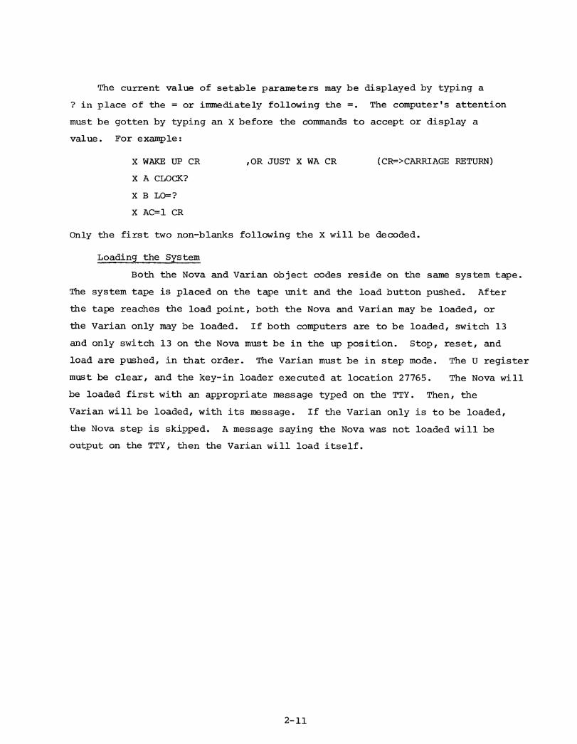
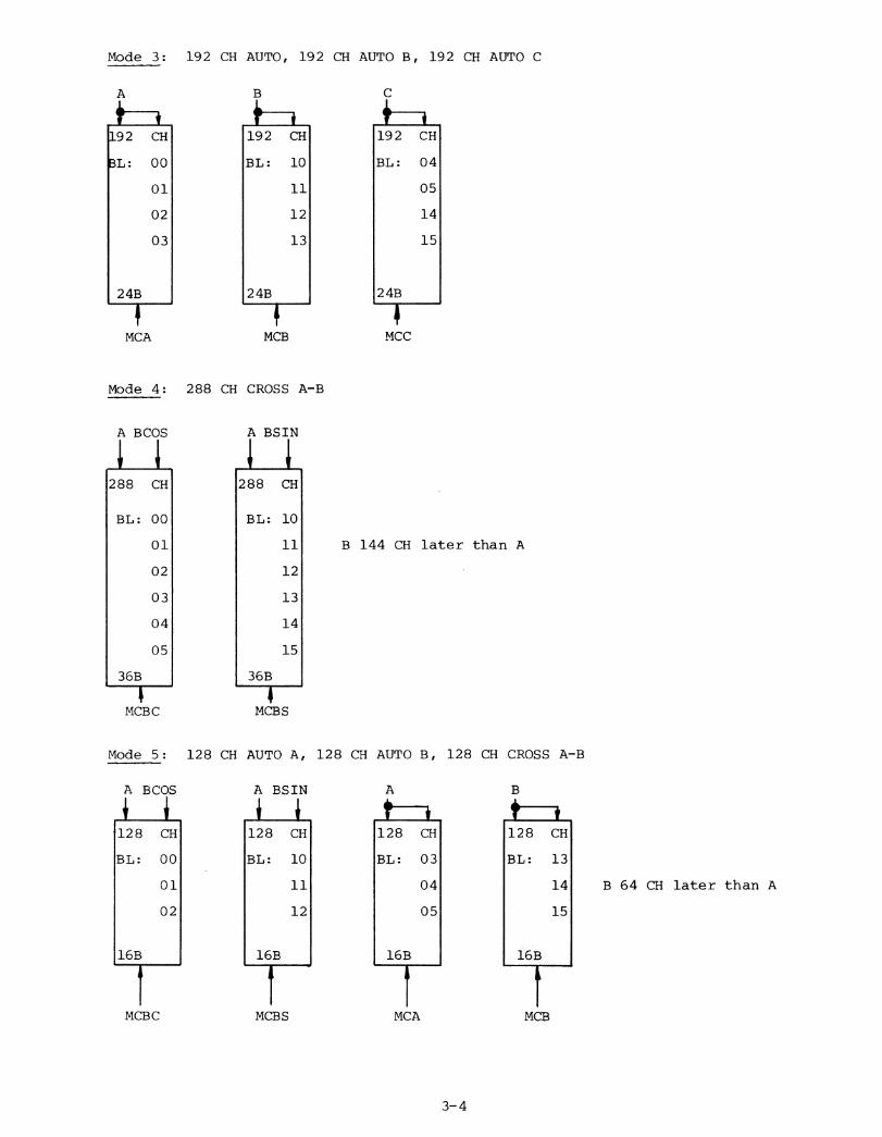
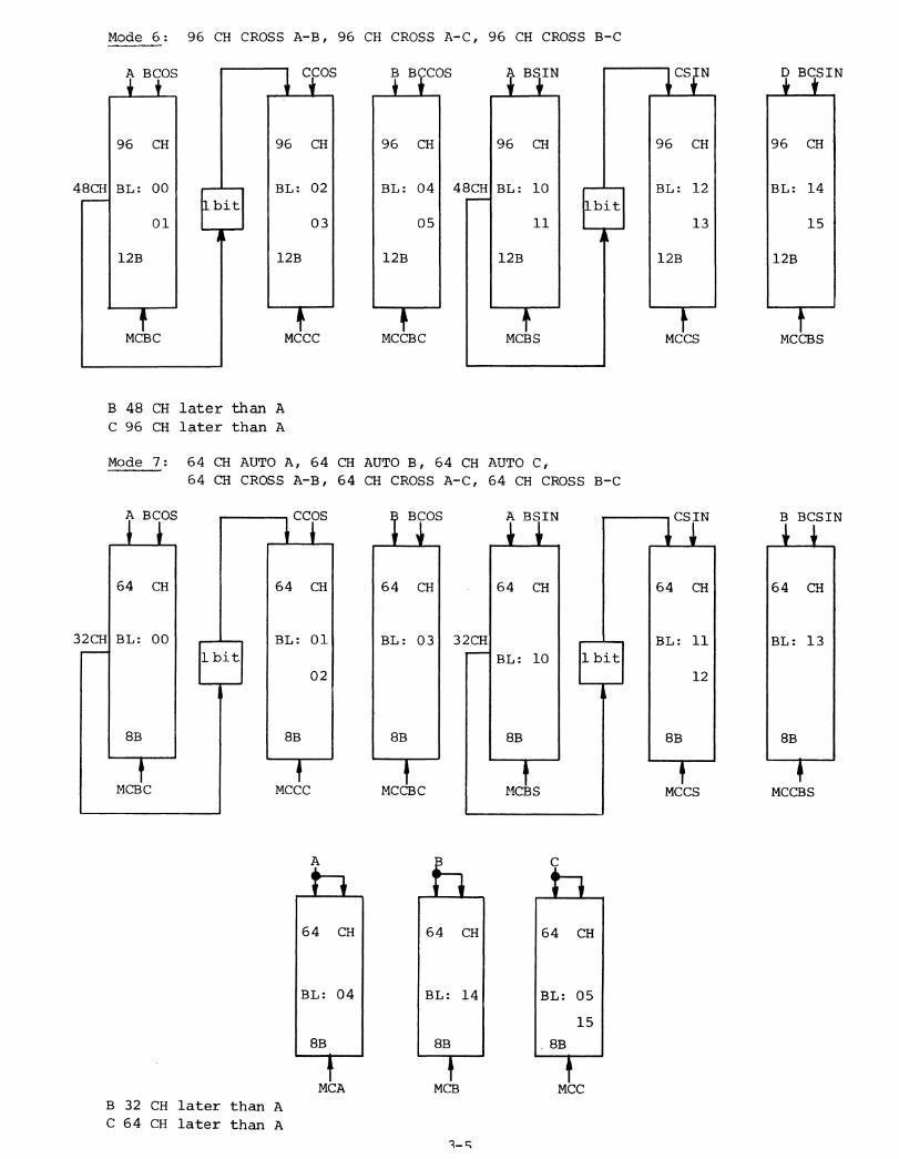
of 576 channels which are arranged in one of 8 modes as shown in Figure 1.11.
In addition to those channels there are 9 total count channels plus 16 channels
which may be placed in parallel with any of the others under program control.
MODE CORRELATOR
0 - 96 CH AUTO A, 96 CH AUTO B, 192 CH CROSS A-B
1 - 288 CH AUTO A, 288 CH AUTO B
2 576 CH AUTO A
3 192 CH AUTO A, 192 CH AUTO B, 192 CH AUTO C
4 288 CH CROSS A-B
5 128 CH AUTO A, 128 CH AUTO B, 128 CH CROSS A-B
6 - 96 CH CROSS A-B, 96 CH CROSS A-C, 96 CH CROSS B-C
7 < 64 CH AUTO A, 64 CH AUTO B, 64 CH AUTO C64 CH CROSS A-B, 64 CH CROSS A-C, 64 CH CROSS B-C
Figure 1.11 Correlator Modes
There are three 3-level fringe rotators similar to the one described in EDIR #118.
Fringe rotator A-B and A-C are independently controlled by the program whereas
fringe rotator B-C takes the phase difference of A-C minus A-B.
Sample rates are controlled by the program and correspond to the bandwidths:
2 MHz, 1 MHz, 500 kHz, 250 kHz, 125 kHz, 62.5 kHz, 31.25 kHz and 15.625 kHz.

hut
Li- r
---- A
.......
c
MCC c
hoc
1 , cos c
os' c
ps
Pio
DE
T*01
162
0
riPLE
Rh
A .V
M-P
LO c 2011
Ht.
X- T
A I
OH
L
L.r-
Tie
.IN
RoM
/01Z
IPP
e -F
P S
FY?
Oti
IPC
H
t wc.
t.W
Ctv
oikt
LI
COP
TO 62.0
1
riP
LE
k.5'
441
PaC
AN
PLE
P
rppk
u. P
ATE
:D
G•L
AY
Dq
rt.i
.r/
C.
r E.
R.
AM
Dto
A E
t C
Ftz
oti v
t t.
t E
t R
.,T
O 6
10
I
71-1
, t
C. D
IA PO
CW
rri
. .1.
; rO
W. E
WE
:
..roo
re,
1
e C
19 4 /
MEL
Co
kA
-TO
P
co
siN
G C
HA
NA
/6
Tyzo
ti6
ZO TR
oti
()to'
API
A x
icE
-
R&-
TA
C K
T
IRP
T
TO
6?
oi
60
1it
rPO
ttO
FF
E 0
DP
A,B
,C I.T
O M
I
rz e
s E
T-i
kon
6'2,
01
DP
4
bP
e
bP c
rkott
rtgr
fER
CS
DA
TA
TO
ru
rre
vz
1.1.
467 O
V

Specification of FFT Processor
The FFT consists of a Nova 820 CPU, an Elsytec 306/MFFT plug-in
array processor and a program library supplied by Elsytec. It is a mediumspeed FFT processor with the following basic specification:
No. Real Points 32 64 128 256 512* 1024 2048 4098 8192 16384Time/ms 8.8 14.5 23 39 75 139 280 600 1300 2850
No. Core Locations 58 114 226 450 898 1794 3586 7170 14338 28674
*Used by NRAO
These times are without I/O transfers and without set-up by a master program.
NRAO has added fractional bit shift corrections to the master program. Forfurther details see Chapter .2.
1-15
CHAPTER 2: Software
Introduction The present configuration for VLBI processing consists of a Varian
620-1 minicomputer and a Data General Nova 820 minicomputer. The Nova containsan Elsytec array processor hardware board which permits it to fast Fourier
transform the cross-correlation function sent by the Varian and to return theresultant spectrum back to the Varian where it is written on 9 track magnetic
tape.The Varian is, in general, the same software which has been around since
the processor has been in operation. Therehave been extensive modifications,
however. These modifications add to, rather than alter the original philosophy.The first task for the Varian program is to read into memory the PREPTAPE
information. This consists of up to 20 scans. The video tapes should be positionedto within one second of time relative to each other. When the start button is
pushed on the correlator chassis, the program starts the video tape players(either 2 or 3), insists on 30 consecutive good frames, then aligns the tapesto the sane frame number.
The delay between station A and B is calculated and strobed in. If thereis a third station the A-C delay is calculated and strobed in. A built in delayof 5 seconds must elapse before data are recorded on 9 track tape. If mode 0or 4 is in effect, the correlator data are sent to the Nova computer to betransformed, then sent back to the Varian to be written on tape.
A CRT display of fringe amplitude for 12 channels of A-B data and 12 channelsof A-C data is created by the Varian. In case of two station processing, 24channels of A-B data are displayed.
The source statements for both the Varian and Nova computers contain manycomments which make the programs self-documenting.
NOVAEDIT and VAREDIT
As an on-line aid to debugging, simple editing programs have beenwritten for the Varian and Nova oomputers. These are very similar in use.They allow a programmer to assemble, set and clear break points, type out
in various formats selected portions of core, move selected portions of core,
and to begin executing a program at a given location. The editing instructions
are slightly different for the two systems.

(ASSEMBLE)
(SET BREAK POINT)
(CLEAR BREAK POINT)
(DECIMAL FRACTION TYPE-OUT)
(FRACTIONAL FRACTION TYPE-OUT)
(INTEGER DECIMAL TYPE-OUT)
(INTEGER OCTAL TYPE-OUT)
(TYPE-OUT 2'S COMPLEMENT OCTAL)
(TYPE-OUT UNSIGNED DECIMAL (16 BITS))
(JUMP-TO (BEGIN EXECUTING))
(MOVE CONTENTS OF SELECTED LOCATIONS)
(ZAP BREAK POINT (CBP, NO ADDRESS RESTORATION))
NOVA VARIAN
A A
SBP
CBP
(NA)
(NA)
TSD
0 TS0
TUO
(NA) TUD
JMP
MOV
ZBR
The assembler mimics the cross assemblers but does not permit the use of
labels. All addresses must be relative to the P register or must be absolute.
The instructions to the EDIT programs are in the form of function, Address 1,
Address 2, and in the case of MOVE, N. Some examples follow.
A 1000,1020 Assemble from locations 1000 through 1020.
Types out in 2's complement octal location 12345(Type unsigned octal)
Types out in integer decimal locations 15 through 20(Type signed decimal)
Accepts fractional decimal in the form + or - .DDDDDwhere DDDDD refers to decimal digits
T 12345 orTUO 12345
I 15,20 orTSD 15,20
F 17000
M 100,200,20 or Will move locations 100 through 117 to locations 200NOV 100,200,20 through 217
B 1025 orSBP 1025
C 1025 orCBP 1025
Z 1025 orZBP 1025
O 1777,2001 orTS0 1777,2001
D 20000
J 2040 orJMP 2040
Will set a break point at location 1025. Location1026 will be used also
Will restore locations 1025 and 1026 to originalvalues
Will clear the break point switch without restoringlocations 1025 and 1026
Types out in signed octal locations 1777 through 2001(type signed octal)
Types out in signed decimal fraction location 20000
Will jump to location 2040

N locations of core may be set to a constant value (including zero) by
assembling the constant into the first location of the array then moving N-1
values from the first location to the second location.
EX. A 1000 (Ember constant into location 1000)
M 1000,1001,077 (Will propagate the constant from 1001through 1077)
All instruction to the EDIT programs are terminated by a carriage return.
NOVAEDIT restricts mnemonics to three characters. Changes from
cross-assembler follow:
ORIGINAL NOVAEDIT
INTEN INE
INTDS IND
SKPBN SBN
SKPBZ SBZ
SKPDN SDN
SKPDZ SDZ
READS RDS
INTA INA
MSKO MKO
IORST IOR
HALT HLT
Nova Subroutines
1. AGET Accepts a character from input device.
2. APUT Outputs a character on the output device.
3. ATYPE Types the value in RO in 2's complement octal.
4. TNCR Types message in address following call
Entry ATNCR No LF-CR
Entry ATLCR LF-CR before typing
Entry ATFCR LF-CR after typing
5. AWLIM
6. ASHFT
7. ASRA
Compares value of RO with limits directly followingcall. Lower limit is first, then upper. Returnis to next location if outside limits; and to thenext + one if within limits.
Logically left shifts RO by amount following call.
Arithmetically right shifts RO amount following call.

Nova Subroutines (cont.)
8. ASLA Arithmetically left shifts RU by amount following call
9. ASRL Logically right shifts RO by amount following call.
10. ASLL Logically left shifts RO by amount following call.
11. ADSLA Arithmetically shifts left the contents of thedouble precision value as addressed by the nextlocation.
12. ADSLL Logical left shift version.
13. ADSRA Arithmetic right version.
14. ADSRL Logical right shift version.
15. AFSUB Double precision subtract of next address from nextplus one. If overflow, return is with carry set.
16. AFADD Double precision add.
17. AFMUL Single precision multiply with double precision result.Address following call is multiplied by address followingthat. DP product is placed in following address.
18. AFDIV A double precision dividend is divided by a single precisiondivisor resulting in a single precision quotient. Divisorfollows call, then dividend, then quotient. Quotient+1contains remainder. Return is with carry set if overflow.
19. FSCAL Arithmetically shifts right the value in RO. The resultis rounded rather than truncated. Accepts positive ornegative numbers.
20. AMOVE Moves one or more contiguous words from one location toanother. 'FROM' address follows call, then 'TO' address,then 'N' words to move. 'N' is octal.
21. ANORM Normalizes a binary fraction with contiguous exponent.Address of fraction, exponent follows call.
22. AFN1 Calls MFFT routines. Function to do follows call, thenPSI 1, then PSI 2, then PSI 3. MWDCT (page zero) mustcontain the negative number of elements to do. Beforecall, RO contains address of operator, R1 containsaddress of operatee, R2 contains address of result.
23. AFMTH Calls meet arithmetic routines. Following call, theaddress contains the function code, next is addressof operand 1, next is address of operand 2, then addressof result. Operand 1 is performed on operand 2.
24. LCARG Computes cosine of value in R2, expressed in binary anglemeasurement (BAM). Upon return RO contains result.
25. LSARG Computes sine of value in R2.
26. LBARG Computes sine and cosine of value in R2.
27. For more subroutines see the Elystec MFFT User's Guide.

Nova Pro9ram
The Nova's sole purpose is to transform the cross-correlation functions
into complex spectra. The Varian reads the correlators every 200 msec., andsends the correlation functions to the Nova following each read. Modes zero and
four are the only modes available to the spectral line user. Mode zero has 192
channels of A X B or a total of 384 sines and cosines. Mode four has 288 channels
of A X B or a total of 576 sines and cosines. A 512 real point transform is taken,so in Mode 4, 64 points are ignored, and in Mode 0, 128 points are cleared to zero
before the FFT.
The Nova is a complete slave to the Varian; that is, all tasks are initiatedby the Varian. During idle moments, the Nova is in a tight wait loop, with its
interrupts enabled, waiting on an interrupt from the Varian. There are threeexpected commands from the Varian. The first is an initialization command which
is generated by the Varian at Varian set-up time. This occurs when the Varian
is syncing the tapes as during scan changes. The cosine table for the FFT is
computed at this time and some minor initialization is done. The other two
expected interrupts are when the Varian is ready to send data and receive data.
When data transfer occurs, it is done one word at a time. One computer sends
a word to the other, then waits until the other has received it before another
word is sent. When the Varian is sending, it is in interrupt enable state and
will be interrupted out of this 'SEND' mode before all data have been sent. This
is no problem, except the actual time required to send data is somewhat greater
than if the Varian could devote its undivided attention to the task. As soon
as the Nova has received all the data, it immediately begins to work on it.
There are four tasks to be performed:
1. Normalize the data by total counts and scale them.
2. Arrange the data in the proper mode, including insertingzeros or discarding data, as necessary.
3. Perform the FFT.
4. Perform the fractional bit shift (FBS) correction.
The cosine and sine total counts are divided by PI, then all cosine values
are divided by cosine TC/PI and sine values are divided by sine TC/PI. Prior
to this division, cos TC/PI and sin TC/PI are normalized, that is, they are
shifted left until the most significant bit (MSB) is set (since they are all
positive). Actually, they are both shifted the same number of bits, the greater
of them making the decision of how many bits to shift. This assures no over-
flow during the normalization divide step, there being no overflow indication
on the Nova.
The data arrangement consists mainly of dividing the input array down
the middle, moving the firsthalf to the latter half of the array to be trans-
formed, and likewise moving the latter half of the original array to the first
half of the array to be transformed. In mode zero, zeros are inserted into the
middle of the new array, and in mode four, the last 64 points of the original
array do not participate in any portion of the task.
The third task is simply the forward or inverse fast Fourier transform
of the data. The Elystec FFT subroutine is called, and the resulting spectrum
occupies the space where the cross-correlation function originally was stored.
The complex spectrum can be written as:
S(K)=SR(K)+I*SI(K) where SR is the real and SI the imaginary parts.
The FBS correction transforms S(K) into S' (K)
S' (K)=(SR(K)+I*SI(K)*(cos P(K)+I*sin P(K)) or
S' (K)+(SR(K)*cos P(K)-SI(K)*sin P(K))+I*(SI(K)*cos P(K)+SR(K) *sin P(K))
cos P(K) and sin P(K) are generated recursively as:
cos P(1) = 1
sin P(1) = 0
cos P(K) = cos P(K-1)*cos DELTA-sin P(K-1)*sin DELTA
sin P(K) = sin P(K-1)*cos DELTA+cos P(K-1)*sin DELTA
DELTA = PI*FBS
FBS = (TRUNC DELAY-TRUE DELAY)*BAND WIDTH/2000/N
N = SAMPLING INTERVAL = 0.25 micro seconds
Only the first 128 complex points of the spectrum are kept. The remainder
are set to zero.
The actual beginning of the program is at entry 'DWAIT'. The first thing
there is to disable the interrupts. 'DLOOP' busy switch is setnot busy, the
interrupts are enabled, and the computer stays in a jump to itself instruction.
When an interrupt occurs, 'DSERV' routine is reached. Here, all registers
and the status of the carry bit are saved. If the Varian interrupted with
code '0', 'DINIT' routine is called. If this entry is the first since the
program was loaded, a cosine table for the FFT is calculated. Several countersare zeroed, and a table of cosines is calculated for possible Harming weighting.
The program then returns to 'DWAIT'.
If the Varian interrupts with code '2', 'DSEND' routine is called. This
is the routine which sends the computed spectrum to the Varian. The spectrum
has been placed in a buffer array and is safe from other routines. The data
are sent, one word at a time, to the Varian. The Nova sends a word, then
repeatedly asks if the Varian has received it. If more than a predetermined
number of 'ASKS' occurs, the Nova gives up and goes back to 'DWAIT'. This
probably means the Varian got into trouble and interrupted itself and had to
resync. If the Nova successfully sends the complete spectrum to the Varian,
it calls 'DOVER' routine. Here, the registers and carry bit are restored to
values they contained before interruption, then return is back to location where
the interrupt occurred.
Code '1' interrupt is where the real work is done. This is when the Varian
wants to send a correlation function to be transformed. The Nova reads each
word, tells the Varian it has read the word, then waits for the next word. The
Nova's interrupts are disabled during this time, but each word is checked for
a command word, so if the varian has gotten itself lost and has to restart, the
Nova will be prepared for it.
Following successful data transfer, the Nova re-enables its interrupts,
then enters 'DLOOP' routine. A busy switch is checked to see if the Nova hadbeen interrupted out of this routine. This is a catastropic situation if it
happens, so the Nova just stops. Operator intervention is necessary to restartthe system. Normally, 'DLOOP' will not be busy and processing will continue.The first 53 words are moved from the input array to the working array for
safekeeping. These are not the correlation function, but are parametersnecessary to the Nova and the post-processing programs. The busy switch isset busy.
The correlation function is moved to the working array, divided in half,
and the middle zeroed or portions ignored, depending on mode. Several switches
are set or reset depending on sideband, Hanning weighting, and FBS correction.
Delta is computed in binary angle measurement (1M), cos and sin of total
counts are divided by PI, normalized, and the reciprocal taken. The data to
be transformed are checked to determine the largest Absolute-value. All data
are shifted left by the amount needed to normalize this value. This insures
maximum precision. All odd numbered values (cosines) are multiplied by the
reciprocal of the cosine of total counts and all even numbered values (sines)
are multiplied by the reciprocal of the sine of total counts. Exact count is
kept of all scaling.
The sign on the transform is determined by which sideband is called for.
As a note, the Nova's inverse FFT corresponds to the subroutine Fourg's forward
FFT. The call to the Nova's FFT is straight forward. Some addresses must be
inititalized, the number of points must be set, then a standard subroutine jump
is used. The transform is done in place; that is, the spectrum occupies thearea where the correlation function once resided.
A check is now made on whether to do the FBS correction, If it is to be
done, much use is made of the Elystec's array arithmetic capability. This
uses a greater amount of core, but is much faster. In fact, without using
arrays, the FBS takes too long and the task cannot be completed within the
allotted time. Cos and sin of delta are calculated, then a table of cos P
sin P is generated.
The product arrays, cos PRE, sin P*RE, cos P*IM, and sin PPE are computed,
128 at a time. Then the real and imaginary parts are updated in place.
Finally, unused words in the array are set to zero. This happens even if
the FBS correction is not being done. The 'DLOOP' busy switch is cleared, and
the program switches back to 'DWAIT' and loops there until the next interrupt
occurs.
Varian Program
The Varian program types out a message informing the user of the
current system date, then halts. When the computer run button is pushed, the
Varian reads PREPTAPE information into core, then waits for the correlator
start button to be pushed. The video tapes should be aligned to the same
second of time and be in remote control. When the correlator start button
is pushed, the VArian starts the video tapes, waits for 30 good frame counts
to come in, then synchronizes the tpaes to the same frame count. Delays are
computed, strobed into the correlator and correlation begins.
The Varian enables its interrupts, then waits in a tight loop for an
interrupt to come in. Interrupts occur 60 times per second, or at a
16.66666667 millisecond rate. This is the innermost loop of the program.
Other loops are at 100 millisecond and 200 millisecond intervals. At the
100 millisecond interval, delays and rates are computed for the next 100millisecond interval. The values for the 60 Hz interrupts are derived bylinearly interpolating between the values computed for 100 millisecondintervals. At the 200 millisecond interval, data are either passed to theNova for transforming or written directly on 9 track magnetic tape.
At each 60 Hz interrupt, 'VLOOP' runs the assured clock on the framecount. This assures the program that the frame count difference between
A7-13 and A-C will not be affected by bad frame counts that occur only rarely.A series of bad frame counts will throw the program back into re-sync condition.Audio I is read for one recorder at each 60 Hz interrupt.
Every six 60 Hz interrupts (100 milliseconds) delays and rates are computed.
If the Nova is to be used to transform data, at one of these 100 millisecondintervals, data are sent to the Nova and at the next interval, the previousdata are read from the Nova. The assured clock is run for complete timerather than frame counts as in the 60 Hz loop.
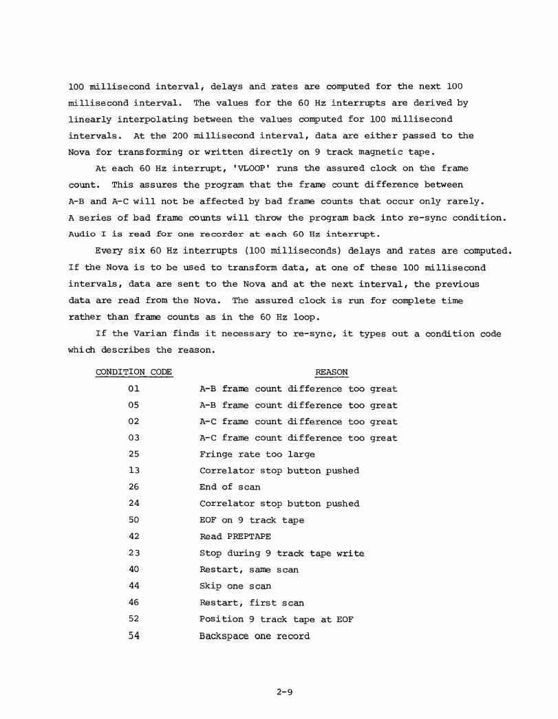
If the Varian finds it necessary to re-sync, it types out a condition codewhich describes the reason.
CONDITION CODE REASON
01 A-B frame count difference too great05 A-B frame count difference too great02 A-C frame count difference too great03 A-C frame count difference too great25 Fringe rate too large13 Correlator stop button pushed26 End of scan24 Correlator stop button pushed50 EOF on 9 track tape42 Read PREPTAPE23 Stop during 9 track tape write40 Restart, same scan44 Skip one scan46 Restart, first scan52 Position 9 track tape at EOF
54 Backspace one record

CONDITION CODE REASON
56 Type current scan number and time
17 Position 9 track tape at end of data
62 Enable channel checking
64 Disable channel Checking
10 Buffer fault on recorder C
11 Buffer fault on recorder B
12 Buffer fault on recorder B
30 Program interrupted itself. If in 3 station modeand addresses typed after CC are identical, probablya parity error occurred on 9 track tape and there wasnot time to correct it.
If switch 1 is up, certain parameters may be entered from the teletype.
These are:
B DELAY=DDD CR ACTUAL CHARACTERS DECODED BD
C DELAY=DDD CR (DDD=>DECIMAL DIGITS) CD
A CLOCK=DDD CR (CR=>CARRIAGE RETURN) AC
B CLOCK=DDD CR BC
C CLOCK=DDD CR CC
B LO=DDD CR BL
C LO=DDD CR CL
NOTE MESSAGE ........... CR....................................................................... NO
EOF CR EO
FIRST SCAN CR Fl
ENABLE CHECKING CR EN
DISABLE CHECKING CR DI
DATA END CR DA
SKIP SCAN CR SK
READ PPEPTAPE CR RE
TYPE SCAN NUMBER CR TY
START STOP TYPE CR ST
WAKE UP ALERT CR WA
The current value of setable parameters may be displayed by typing a? in place of the = or immediately following the =. The computer's attentionmust be gotten by typing an X before the commands to accept or display avalue. For example:
X WAKE UP CR ,OR JUST X WA CR (CR=>CARRIAGE RETURN)
X A CLOCK?X B LO=?X AC=1 CR
Only the first two non-blanks following the X will be decoded.
Loading the System
Both the Nova and Varian object codes reside on the same system tape.The system tape is placed on the tape unit and the load button pushed. After
the tape reaches the load point, both the Nova and Varian may be loaded, or
the Varian only may be loaded. If both computers are to be loaded, switch 13and only switch 13 on the Nova must be in the up position. Stop, reset, and
load are pushed, in that order. The Varian must be in step mode. The U registermust be clear, and the key-in loader executed at location 27765. The Nova willbe loaded first with an appropriate message typed on the TTY. Then, theVarian will be loaded, with its message. If the Varian only is to be loaded,
the Nova step is skipped. A message saying the Nova was not loaded will beoutput on the TTY, then the Varian will load itself.

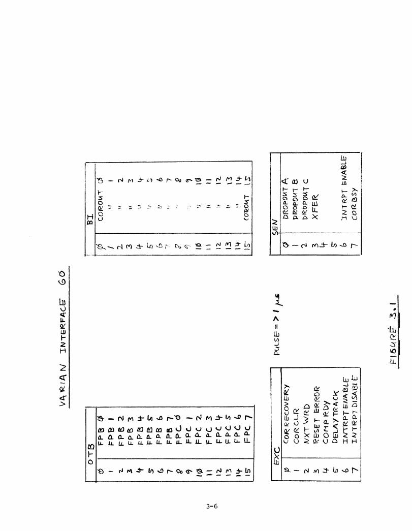
CHAPTER 3: System Interconnection and Computer I/O's
This chapter describes the interface between the correlator and the Variancomputer. Organization of the correlator is described as seen by the computer.The 8 correlator modes are shown including the sequence in which data is
presented to the computer. All I/O control and monitor lines are shown in3.1 to 3.6. Also, all critical timing that has to be considered by the
program are detailed.
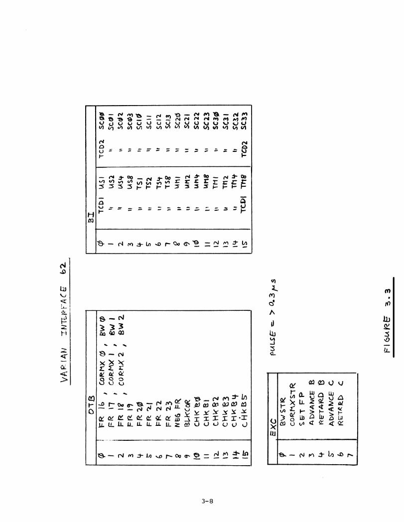
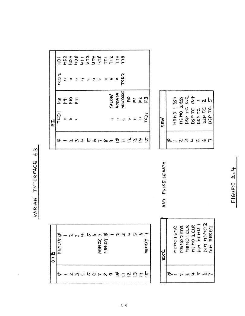
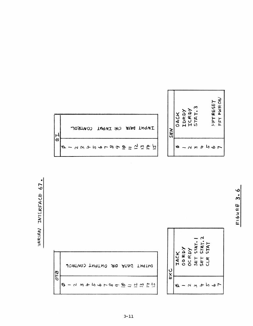
All cables that interconnect all chassis, computer and tape recorder arelisted in detail in the blueprints. There are six general purpose I/Oconnections to the computer which have fixed assignments. They are shownin Figures 3.1 to 3.6.
Timing the decoded audio is important for the program. It takes up to34 msec. for new data to be ready after a select command. Also, timing formemo X, Y and Z needs to be considered by the programmer. X and Y need tosettle 15 psec for full scale deflection before Z may be turned on. After
Z pulse is executed it takes 30 psec for a point to print on the screen.During that time X and Y should not be changed and no other EXC 63 shouldbe executed. All other outputs are not critical for timing.
The correlator is read out per block and card in a fixed sequence:
TC AUTO ATC AUTO BTC AUTO CTC CROSS A-B COS
TC CROSS A-B SINTC CROSS A-C COS
TC CROSS A-C SIN
TC CROSS B-C COS
TC CROSS B-C SIN
BLOCK 00 64 CHBLOCK 01 32 CHBLOCK 02 32 CH
BLOCK 03 64 CHBLOCK 04 64 CH
BLOCK 05 32 CH

BLOCK 10 64 CH
BLOCK 11 32 CH
BLOCK 12 32 CH
BLOCK 13 64 CH
BLOCK 14 64 CH
BLOCK 15 32 CH
CHK 0 8 CH
CHK 1 8 CH
TERMINATOR

288 CH
BL: 00
01
02
03
04
05
36B
MCA
Depending upon the mode selected the blocks are arranged in the followings ways:
Mode 0: 96 CH Auto A, 96 CH Auto B, 192 CH Cross A-B
A BCOS_
192 CH
BL: 00
01
02
03
24B
MCBC
A BSIN
192 CH
BL: 10
11
12
13
24B
MCBS
96 CH
BL: 04
05
12B
MCA
h96 CH
BL: 14
15
12B
MCB
Mode 1: 288 CH Auto A, 288 CH Auto B
288 CH
BL: 10
11
12
13
14
15
36B
MCB
Mode 2 : 576 CH Auto A
576 CH
72B
MCA
BL: 00 10
01 11
02 12
03 13
04 14
05 15
B 96 CH later than A
A
192 CH
BL: 00
01
02
03
24B
192 CH
BL: 10
11
12
13
24B
MCA MCB MCC
192 CH
BL: 04
05
14
15
24B
f f 4
A BCOS
288 CH
BL: 00
01
02
03
04
05
36B
A BSIN
288 CH
BL: 10
11
12
13
14
15
36B
B 144 CH later than A
128 CH
BL: 03
04
05
16B
128 CH
BL: 13
14
15
16B
A BCOS
128 CH
BL: 00
01
02
,16B
A BSIN
128 CH
BL: 10
11
12
, 16B
B 64 CH later than A
Mode 3: 192 CH AUTO, 192 CH AUTO B, 192 CH AUTO C
Mode : 288 CH CROSS A-B
MCBC MCBS
Mode 5: 128 CH AUTO A, 128 CH AUTO B, 128 CH CROSS A-B
MCBC MCBS MCA MCB
CSN
96 CH
48CH ■■•■•■•■■■■■11 BL: 12
13
12B
lbit
MCCBSMCCC MCCBC MCBS
A BSIN
96 CH
BL: 10
11
12B
BiCOS
BL: 04
05
12B
COS
96 CH
BL: 02
03
12B
BCtSIN
96 CH
BL: 14
15
12B
B BCSIN
64 CH
BL: 13
8B
96 CH
MCCBS
CSIN
64 CH
BL: 11
12
8B
A BCOS
64 CH
32CH BL: 001 bit
8B
1MCBC
MCA MCC
Mode 6: 96 CH CROSS A-B, 96 CH CROSS A-C, 96 CH CROSS B-C
48CH
P4i BCsOS
96 CH
BL: 00
01
12B
MCBC
lbit
B 48 CH later than AC 96 CH later than A
Mode 7: 64 CH AUTO A, 64 CH AUTO B, 64 CH AUTO C,64 CH CROSS A-B, 64 CH CROSS A-C, 64 CH CROSS B-C
32CH
CCOSI 64 CH
BL: 01
02
8B
MCCBC
A BSIN
64 CH
BL: 10
8B
MCBS
■•■■■••■■•■=11M1.11
1 bit4••■••.1...■
B 32 CH later than AC 64 CH later than A
1-C
ViN
YV I
NTerr
Ac-
Ue*
Gc
puLsE >
I ti
ts
0T3
0 I 2 - 3 I f g 6 7 p 9 1 0 t i )1 13 )L1. Is-
FP B
CA
PP
RI
FP
it
21
FP e
,3
PP
a 4
pP
B s
-F
PB
6F
PB
7F
PC
dPP
C.
1r
Pc 2
.F
PC
3r
Pc
Li.F
PC
S'
FP
C 6
F P
C 7
L-)(c
.P I 2 L i.
&-- 6 7
cok
RE
CO
VE
RY
Co
R C
UR
IV>
CT
wR
Dr
EsE
T-
RIR
otz
cori
P R
t>y
DE
LA
Y IR
A c
ipc
Tiv
-TR
pT N
A-e
LE
INV
2P
7-
bt.
SA
I?d, r
SE
N01
10P0
(AT
pRop
ow
t e
1>Ro
pot
AT
c3
xF
ER
s-iN
TR
PT
t•/
Ael
.E-
Cor
z i3
sy
3.1

AN
Y K
ase
L5N
&T
I-f
0 1 2 3 4 r & i A
AL
E/2
1- D
PP
eX
C
0 I 2 3 t t g" b 7
....st
-L1
ci>
4se
- L
TC
1) 8
sEL:
wr C
b C
.S
ET
FA
aS
ET
FR
CA
LE
IZT
oFr
AL.
RT. e
`WA
A L
zwr
.
VARIAt4 IN
- MIZ
FA
Cli
6 I
0- T
a
0 1 3 L I-F
R I f-
S-5
66
77
22
96)
101 0
IIII
12_
12(3
1314
-1 t i-
1 rR
IS-
8I.
0 I 2 3 I t 5- 6 7 g 9 115
ii
12-
1 3 li t% $
,
7CD
1 V
H )
141.4
t-t2.
t%lot
h i t
II(4
11
2
LiTH
1%I
TH 2.
ti11-
11 1ti
TH
9
i tPO
tiP
itl
P2
IIP
3
liP
ittp
PS-
IIP6
"T C
OI
P7
TC
D 2
SC40
IfSc4
.1
ItSc1
+2
ItS
C 4
3it
sc s
o1,
sc .5
1if
sc 5
2if
scs3
ilIA
D I
iiuD
2"
Li
to 4
ifIA
De
IfTD
11,
11)2
1,TD
L-1'
CD
21D
8
07
8
R )
6C
oRM
XEW
CP
FR
1/
C0R
,M)e
I€
W1
copfl
x2 1
8W
2.
31,
P R
20
FR -
LIR22
1= R
23
NEG
913
1.1<C
oRC
H K
tO
IIC.
11Vi
c et
132
13C
I-1k
E 3
1Lt
cet
+ s-
P(A
L&
T>
0.3
p.4
$E
xC ew co
tzt-
ws-
rR2
FP
3A
DV
AN
CE
gR
e- T
A-R
D e
s-A
DV
AN
CE
CR
uT
j C
VA P
A
N :
Wit
PF
AC
g
i>
13
1I
0 I 2. 3 L t. s 6 1 e 9 Id II 12.
13 14.
tg
TCD
1II 11 11 11 if II I, it ti 1/ t' it 4 ti TC
I) I
AI
lAS2
1A51
+IA
S8
TS i
112
•si
t
1.S
E
tif ti
I
tAM
2uhtt
Lim
eT
ill
1112
Tt14
-TY
1 9
"T C
D2
11 II 11 II It it tt 1f tI to %I i, 0 itTC
D2
SC
00
Sc.0
ISC
O2
SCO
3sc
i 0sc
.' 1
scrz
SC
I3
sc20
Sal
SC
22
SC I
3S
C30
SC31
SC12
,S
C33
VA
R I
AN
itv
- MR
.FA
Cq 6
3
AN
Y P
IALS
G L
EA/6
111
OI I
S0 I Z 3 ti" g 6 7 g 9 10 II 11 13 14
-,
is-
int-t
Os X 0 1 2 3 L
.
S" 6
h P4
OK
7r1
Et-
t0/ 0 I 2_ 3 4 6
her
-to
y 7
Sk*C
.,çi
c 2 3 i i- s- 6 7
vi E
lio
1 S
TR
NW
IC) 2
SIR
vir. 1
0 1
cl.A
.ti
t- Im
o 2.
cue
1)1 t
iri
E ti
0 I
OM
fit
tio2
bil
l Q
ES
ET
RI.
0 I 2_ 3 4 6- G. 7 g 9 10 11 r2.
11 I Lr
_.is
-
TCD
IIA tA 1, ‘i tt ki kt I 1 It
Tcp
i
PS
P9
P 10
PI
CALo/V
NO
DA
TA
New
CO
DE
F0 Ft P2 3
-rc
vz
.
%) tt n il If It , t, tr tl
TcD
1
HO
IH
D2
HD
41-1
D8
Ler 1
Witt
Lyre
TT1
TTZ
T14
"rt 8
......
SEA
/
0 I 2 3 L t.
s-- *7
.
ritR
h 0
1 ny
Vito
zasy
t)sp
--r
c 0
.2D
sp -
cc a
t -i-
Ds
P TC
IA
SP
It.
aO
SP
TC
S-

131.
1-ipcik
0 1
Hrc
4 r
,H
Fc
g 0
1tr
)I
v1
I1)
I
%,2.
I4
.�..
Itl
2., ,I
3I
,t1
I.(3
tt,
L tiI
k,4-
111
4-,
r4
,C.'
1tS
"/
1-IF
CA
(3(
i4P
CA
bk ft
NFC
..13'
ok
Hpc.(
t 9i
I IPi
PT.
..C. 0
f H
FC
C 0
if1
ii,
II
LI1
t I
2-
ti2.
u1
rtr
14
1LI
1t
11(
L f,
I(14
.4
rt'
G--
tiS-
11C
I'/
tH
Fcg p
i<i
HP
C.
tC
. ok
kicc
... t71
.<vik
ncA ,
mkuc-e
1
ritK
IT..C
.A
LAbi
z
3 tf
pL4L
s>
2,4
sac
cCP
Ru
NS
TR
1D
EL
ST
RB
2 3S
EL
HF
C4.9
I fS
eL
HF
c 4
cs-
St.
..11F
C. ti
C
6S
T*
xFE
R
71
cLa.
xP
ER
Sts
/
(0.
STO
P'I
SLE
AV
BSY
213
oFFL
TA
( le
tevi
s)3
eoF
prr
e (
qom
s)L t
rt O
r-F. -L
TC
C 1
6 w
is.)
.5'B
urF
LT
A (
IS
)&
QtA
rrix
.e (
Is)
1elA
rFL
T C
(IS
)
VA
RIA
V I
NT
OZ
PA
CC
: L t-
o-r .1
30 1 2. 3 it 5
-
e 7 8 9 10 11 12
.
13 Ik t
IS
p&L
Ay
t, ti 4 k,, kl ti tl ty tf 11 it ti
i vinA
y
31
SI-G
410
ItSL
EW3
Ii
sS
LE
W I
2.f
Si
LE
W 6
3- 7
sLE\
A/
t if
i8)
st..
/ g
s- (
WO
,t
7I
SL
EW
c.1
10I
SLE
W C
.)I
)f
C L.
kVc2
12.
tSL
EW
C3
13I
SL
EW
Ctf
)kf-
F&
L.6
\4I cs-
(MA
)Is
-I
Rut
h/A
IC,
iY
.uts
ie
YZ,t,t
/VC
INIA
r>2
IA.23
-1021-LN 0) Ind N.1. ZA0 04 imditi.
— (N1 M -3- iI) -0 r- oo Q% s- zi- is) Al 4.4.- 1,1
iiiv)
P.- 0w
07 o zx ),•. as
y a 0 p..., Ck am
Q '; f44' A 0 .-. t t0 t-1 }-1 u) .it. ii.
,s* — (NJ tvi 3- tol 4) r,
•
g4r
e4t--o
10?.,k11..,W 14c,11.110 ?AO VitiCI .1. Ykl.LYIO
-
)S — N m -i- LI) -4) I-- oo q- '
Q.. c--. Ni AlI')
0X
— NI-: ki": I-
X >.. fl: 115.y a 0 0 LA 0(..) gi }-. i.• ce4 CI
0 ill ib ....)I-1 0000U
hi-cts — N pl ...i
.- 14 ...0 i'•

Check bits 0-5 are six control lines which set a multiplexer to select
the position of the checkboard. Their assignments are given below:
CHB BOARD CHB BOARD
0 00 30 40
1 01 31 41
2 02 32 42
3 03 33 43
4 04 34 44
5 05 35 45
6 06 36 46
7 07 37 47
10 10 40 50
11 11 41 51
12 12 42 52
13 13 43 53
14 20 44
15 21 : ) No checkTurns on panel indicator
16 22 67
17 23 70 TCA (TCB)
20 30 71 TCC (TCC)
21 31 72 TCBC (TCBS)
22 32 73 TCCC (TCCS)
23 33 74 TCCBC (TCCBS)
24 34 75
25 35 . I} No checkTurns on panel indicator
26 36 77
27 37
Figure 3.7 Check Channel Assignments
Chapter : Circuit Description
All NRAO designed circuits are built on NRAO digital circuit boards and
mounted in NRAO digital chassis. Figure 4.1 shows chassis layouts. All circuitsare built on wire wrap cards with the exception of the correlator cards, whichhave a two-sided printed circuit card. The following sections describe functionand timing of the circuits whereby the reader is referred to NRAO drawings
#D2.519.
Decoder
All three decoders are identical and interchangeable. They contain
decoding circuits and BOF detector for video data and decoding circuits foraudio data.
Video data are first amplified and phase compensated in the recorder
preamplifier and then clipped within the video recorder. This clipped video
data, the "Astrodata", is the input to the decoder. Astrodata is firstedge detected by a double edge detector which results in 20 ns wide pulses at8 MHz or 4 MHz depending whether a "1" or a "0" has been recorded. A phaselocked loop running at 8 MHz with a time constant of 15 ps locks to these
pulses. 8 MHz is necessary because of an unfortunate choice for the videocode. During the head gap a 4 MHz signal is recorded without polarity
information. A 4 MHz PLL would lock with an ambiguity of 1/2 cycle. At the
first "0" in the data stream this ambiguity is resolved, however the PLL cannotrespond fast enough and BOF would not be decoded properly. Another unfortunatechoice is the 2.66 MHz for BOF and EOF. The PLL has a narrow capture range of+10% so that it is not upset by the 2.66 MHz BOF. Data is decoded by a fast
sampler-decoder whose phase is given by the phase of the PLL and propagation thru
several gates. Adjusting capacitor 8B11 effects the phase of the sampler and should
be adjusted for best decoding with the front panel trimpot on half scale. This
200Q front panel trimpot is a fine adjustment for the PLL. The operator should use
it to compensate for variations in tapes and recorder performance. Detection of
BOF is done with a separate circuit. At every transition of HEADSW a 45 ps
1 shot is fired. This is needed to let the video signal settle from the head-
switch signal. After 45 ps gate 6C6 is enabled by BOFWDW and at the beginning
of the 2/3 clock 6C6 is made and counter 6D, 6E is started. 24 clock pulses
later GATE becomes true thru 5C5. When a 100 pattern is detected in 10D8
BOF becomes true for 100 ns. BOF resets counter 6D, 6E and closes GATE.

SPA
RC
-ke
CoR
DE
R.
CT
RL
1
1)co
DE
I: 4,A
Rec
.oR
DE
Rci
rl2L
2
1st4
FFE
RA
bEco
DE
RC
DE cp
DER
B
WAD
cT
RL
.C
LO
AD
CT
RL
6
LoA
DA
Dcr
ikii
C
ws•
LoA
DC
TRLI
Bum
.0A
bcri
lL 2
.c
UN
LoA
DC
rit 2
BS
PA
RE
.
CPA
reE
SPA
RE
'
SPA
RE
-M
IME
RO
T.
3
SPA
RE
rRio
i6E
Rol
%C
.
SPA.
R•F
Rol
6-C
MA
MA
cli
c
R 1
DEL
Dis
pay
A- e
IIM
FFER
INTE
RFA
CE
FR
/ D
etD
ISM
Ay 4
(T
CC
oto/
TE
Rfi
stio
sco
pe
AL
ER
T
,"T
CO•
tAsP
LA
y
lek0
88
'B
k3
513
40
c/
cwt.
8 1
3
64C
11
tSK
1ii-
ES
320-
164
-01
BK
241
313k5
- le
32(1
-I
IWO
3B
32C
4. cH
K C
AR
Dec
H, co
RR
ELA
T0R
.
I2401
CoA
rrno
ti.
CO
RA
. C
HA
SS
1 c
IC
OR
Rq
CO
NT
RO
LB
UF
FE
R
Bit #
NRZO 2/3 CLK
22 23 24 25 26 27 28 29 30 31 32 33 34 35 36 37
01 OIFOIF1IF2IF3IF4IF5I P1 DID
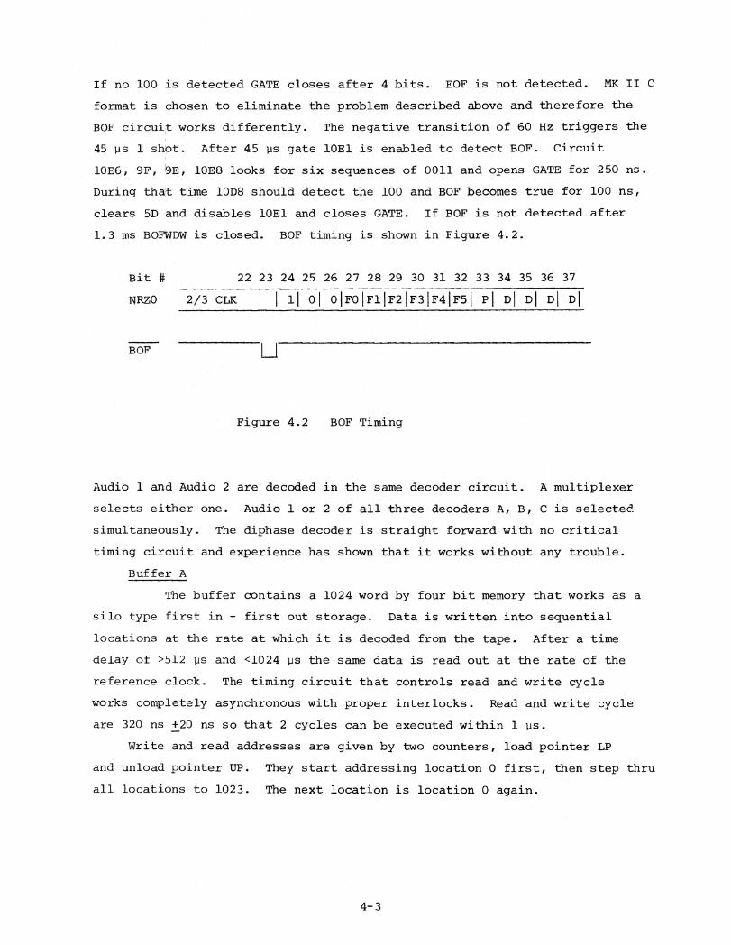
If no 100 is detected GATE closes after 4 bits. EOF is not detected. MK II Cformat is chosen to eliminate the problem described above and therefore theBOF circuit works differently. The negative transition of 60 Hz triggers the45 ps 1 shot. After 45 ps gate 10E1 is enabled to detect BOF. Circuit10E6, 9F, 9E, 10E8 looks for six sequences of 0011 and opens GATE for 250 ns.During that time 10D8 should detect the 100 and BOF becomes true for 100 ns,clears 5D and disables 10E1 and closes GATE. If BOF is not detected after
1.3 ins BOFWDW is closed. BOF timing is shown in Figure 4.2.
BOF
Figure 4.2 BOF Timing
Audio 1 and Audio 2 are decoded in the same decoder circuit. A multiplexer
selects either one. Audio 1 or 2 of all three decoders A, B, C is selectedsimultaneously. The diphase decoder is straight forward with no criticaltiming circuit and experience has shown that it works without any trouble.
Buffer A
The buffer contains a 1024 word by four bit memory that works as asilo type first in - first out storage. Data is written into sequential
locations at the rate at which it is decoded from the tape. After a timedelay of >512 ps and <1024 ps the same data is read out at the rate of thereference clock. The timing circuit that controls read and write cycleworks completely asynchronous with proper interlocks. Read and write cycleare 320 ns +20 ns so that 2 cycles can be executed within 1 ps.
Write and read addresses are given by two counters, load pointer LPand unload pointer UP. They start addressing location 0 first, then step thruall locations to 1023. The next location is location 0 again.
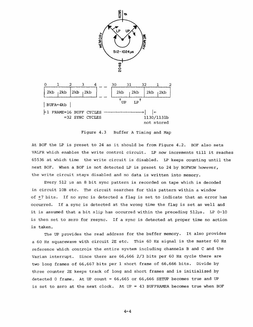
30 31 32 1
I BUFA=4kb
1+- 1 FRAME=16 BUFF CYCLES=32 SYNC CYCLES
0 1
[2kb i2kb 2kb 2kbt
UP LPt
I 14-1130/113lbnot stored
2 3
2kb 2kb
2
2kb 2kb
Figure 4.3 Buffer A Timing and Map
At BOF the LP is preset to 24 as it should be from Figure 4.2. BOF also sets
VALFR which enables the write control circuit. LP now increments till it reaches
65536 at which time the write circuit is disabled. LP keeps counting until the
next BOF. When a BOF is not detected LP is preset to 24 by BOFWDW however,
the write circuit stays disabled and no data is written into memory.
Every 512 ps an 8 bit sync pattern is recorded on tape which is decoded
in circuit 10B etc. The circuit searches for this pattern within a window
of +7 bits. If no sync is detected a flag is set to indicate that an error has
occurred. If a sync is detected at the wrong time the flag is set as well and
it is assumed that a bit slip has occurred within the preceding 512ps. LP 0-10
is then set to zero for resync. If a sync is detected at proper time no action
is taken.
The UP provides the read address for the buffer memory. It also provides
a 60 Hz squarewave with circuit 2E etc. This 60 Hz signal is the master 60 Hz
reference which controls the entire system including channels B and C and the
Varian interrupt. Since there are 66,666 2/3 bits per 60 Hz cycle there are
two long frames of 66,667 bits per 1 short frame of 66,666 bits. Divide by
three counter 2E keeps track of long and short frames and is initialized by
detected 0 frame. At UP count = 66,665 or 66,666 SETUP becomes true and UP
is set to zero at the next clock. At UP = 43 BUFFRAMEA becomes true when BOF
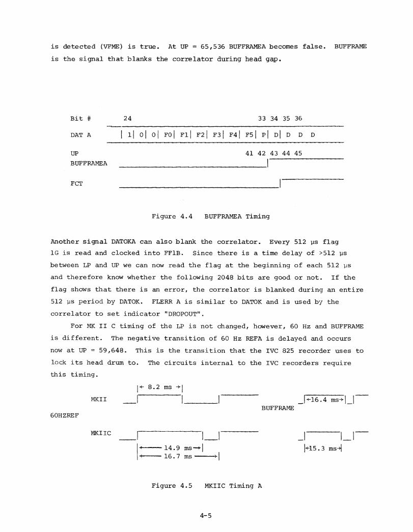
is detected (VFME) is true. At UP = 65,536 BUFFRAMEA becomes false. BUFFRANE
is the signal that blanks the correlator during head gap.
Bit # 24 33 34 35 36
DAT A I 11 01 01 FO( Fit F21 F31 F41 F5 D D D D
UP 41 42 43 44 45BUFFRAMEA
FCT
Figure 4.4 BUFFRAMEA Timing
Another signal DATOKA can also blank the correlator. Every 512 ps flag
1G is read and clocked into FF1B. Since there is a time delay of >512 ps
between LP and UP we can now read the flag at the beginning of each 512 ps
and therefore know whether the following 2048 bits are good or not. If the
flag shows that there is an error, the correlator is blanked during an entire
512 ps period by DATOK. FLERR A is similar to DATOK and is used by the
correlator to set indicator "DROPOUT".
For MK II C timing of the LP is not changed, however, 60 Hz and BUFFRAME
is different. The negative transition of 60 Hz REFA is delayed and occurs
now at UP = 59,648. This is the transition that the IVC 825 recorder uses to
lock its head drum to. The circuits internal to the IVC recorders require
this timing.
1 ÷ 8.2 ms,
F16.4 ms.±1BUFFRAME
60HZREF
MKIIC
ms 1*-15.3 ms-->116.7 ms
MKII
Figure 4.5 MKIIC Timing A

.0
0OD
0-19.9ms
512 -1024 ms
MKIIC furthermore has a shorter frame. BUFFRAME goes false at UP = 61,440.
Since the frame is shorter for MKIIC format the correlator total count will
be slightly smaller.
UP has to trail LP by 512 - 1024 ps. This timing is a function of the
head drum servo amplifier. If phasing is adjusted incorrectly then the
buffer is not working properly. Fault circuit 1B5 detects improper phasing-
timing and sets BFLTA.
Buffer B(C)
Buffer B and C are identical. Each consists of a load control circuit,
a memory, an unload control circuit 1 and an unload control circuit 2. Buffers
B and C have a memory of 81,920 bits - 20.48 ms which handles the same deskewing
task as Buffer A plus a delay of up to 79,864 bits - 19.97 ms which may be
added under program control. This makes it possible to change delay rapidly
(4 ps) and source switching experiments may be processed in one pass instead
of two.
Since 20 ms is longer than one frame, the buffer contains a cycle of five
frames. The write sequence is as follows. The BOF for the first frame, frame 0,
is loaded at location 0. BOF of the next frame is written at location 65,536.
Then when the address has reached 81,920 memory is looped around and location
0 is addressed. The BOF for the third frame is written at location 49,152.
At the beginning of the 6th cycle we start again with writing into location 0.
Figure 4.6 shows the memory map and timing. Similar to Buffer A we have a
load pointer LP and an unload pointer UP but in addition we have a reference
unload pointer REFUP. REFUP lags behind LP from 512 to 1024 ps., UP lags
REFUP by a delay as given by the Varian computer. If that delay is zero then
UP and REFUP are identical.
FRAME 1st BIT1st DATArLAST
BIT
DATA-
BIT DELCT
0.5 0 34 65,535 4
1 65,536 65,570 49,151 3
2 49,152 49,186 32,767 2
3 32,768 32,802 16,383 1
4 16,384 16,418 81,919 • 0i
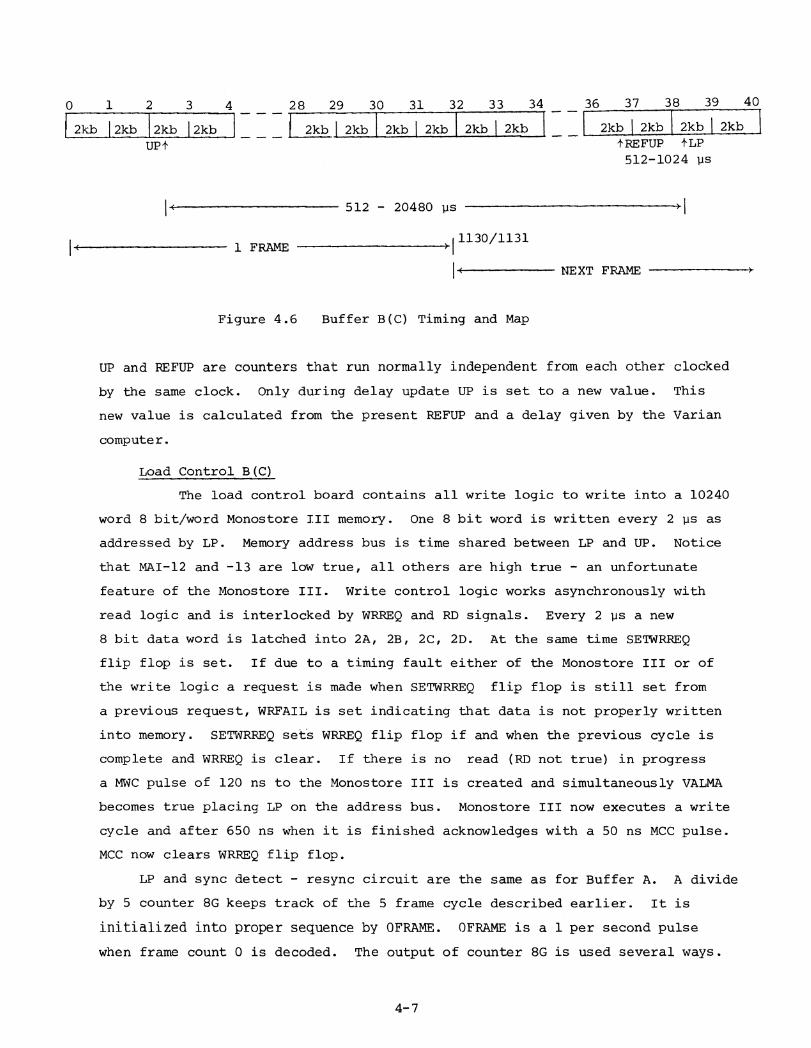
0 1 2 3 28 29 30 31 32 33 34 36 37 38 39 40
/ 2kb 2kb 2kb I 2kb 2kb 2kb 2iL 2kbUP+
2kb [ 2kb 2kb I 2kb tREFUP 4-LP512-1024 ps
512 20480 ps
1 FRAME'1130/1131
NEXT FRAME
Figure 4.6 Buffer B(C) Timing and Map
UP and REFUP are counters that run normally independent from each other clocked
by the same clock. Only during delay update UP is set to a new value. This
new value is calculated from the present REFUP and a delay given by the Varian
computer.
Load Control B(C)
The load control board contains all write logic to write into a 10240
word 8 bit/word Monostore III memory. One 8 bit word is written every 2 is as
addressed by LP. Memory address bus is time shared between LP and UP. Notice
that MAI-12 and -13 are low true, all others are high true - an unfortunate
feature of the Monostore III. Write control logic works asynchronously with
read logic and is interlocked by WRREQ and RD signals. Every 2 ps a new
8 bit data word is latched into 2A, 2B, 2C, 2D. At the same time SETWRREQ
flip flop is set. If due to a timing fault either of the Monostore III or of
the write logic a request is made when SETWRREQ flip flop is still set from
a previous request, WRFAIL is set indicating that data is not properly written
into memory. SETWRREQ set 's WRREQ flip flop if and when the previous cycle is
complete and WRREQ is clear. If there is no read (RD not true) in progress
a MWC pulse of 120 ns to the Monostore III is created and simultaneously VALMA
becomes true placing LP on the address bus. Monostore III now executes a write
cycle and after 650 ns when it is finished acknowledges with a 50 ns MCC pulse.
MCC now clears WRREQ flip flop.
LP and sync detect - resync circuit are the same as for Buffer A. A divide
by 5 counter 8G keeps track of the 5 frame cycle described earlier. It is
initialized into proper sequence by OFRAME. °FRAME is a 1 per second pulse
when frame count 0 is decoded. The output of counter 8G is used several ways.
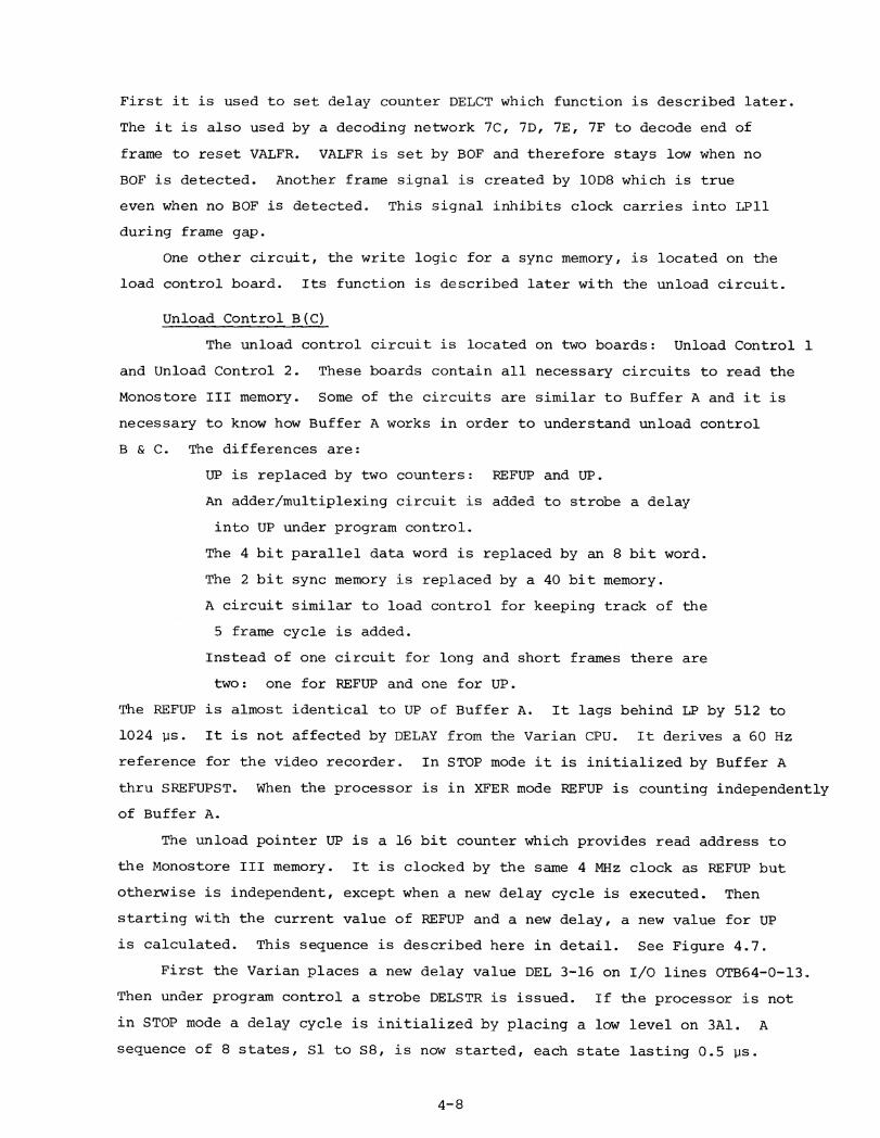
First it is used to set delay counter DELCT which function is described later.The it is also used by a decoding network 7C, 7D, 7E, 7F to decode end of
frame to reset VALFR. VALFR is set by BOF and therefore stays low when noBOF is detected. Another frame signal is created by 10D8 which is trueeven when no BOF is detected. This signal inhibits clock carries into 1211during frame gap.
One other circuit, the write logic for a sync memory, is located on theload control board. Its function is described later with the unload circuit.
Unload Control B(C)
The unload control circuit is located on two boards: Unload Control 1
and Unload Control 2. These boards contain all necessary circuits to read the
Monostore III memory. Some of the circuits are similar to Buffer A and it is
necessary to know how Buffer A works in order to understand unload controlB & C. The differences are:
UP is replaced by two counters: REFUP and UP.
An adder/multiplexing circuit is added to strobe a delayinto UP under program control.
The 4 bit parallel data word is replaced by an 8 bit word.
The 2 bit sync memory is replaced by a 40 bit memory.
A circuit similar to load control for keeping track of the5 frame cycle is added.
Instead of one circuit for long and short frames there aretwo: one for REFUP and one for UP.
The REFUP is almost identical to UP of Buffer A. It lags behind LP by 512 to1024 ps. It is not affected by DELAY from the Varian CPU. It derives a 60 Hz
reference for the video recorder. In STOP mode it is initialized by Buffer Athru SREFUPST. When the processor is in XFER mode REFUP is counting independentlyof Buffer A.
The unload pointer UP is a 16 bit counter which provides read address tothe Monostore III memory. It is clocked by the same 4 MHz clock as REFUP but
otherwise is independent, except when a new delay cycle is executed. Then
starting with the current value of REFUP and a new delay, a new value for UP
is calculated. This sequence is described here in detail. See Figure 4.7.
First the Varian places a new delay value DEL 3-16 on I/O lines 0TB64-0-13.Then under program control a strobe DELSTR is issued. If the processor is notin STOP mode a delay cycle is initialized by placing a low level on 3A1. Asequence of 8 states, 51 to 58, is now started, each state lasting 0.5 ps.

Si: Set DELCYC, clear 3A1, load DELCT from LP circuit
Clear DATOK, disable FLERR
Set multiplexers to do DEL + REFUP + 1 (= REFUP - DEL)
Get carry if result >0 (means same frame)
Get no carry if result <0 (means skip to previous frame or frames)
Next CLK1: Clock up (Load result into UP)
Set SKPFRM1 if no carry
Set S2
Comments: If DEL=0 then we always stay within the same frame. If
DEL is small then we may have to go to the previous frame
depending upon the present REFUP. If DEL > 16.6 ms then
we may have to go two frames back. SKPFRM 1 & 2 keep
track of this.
52: NOOP if no SKPFRM1. If SKPFRM1:
Decrement DELCT with CD
Set multiplexers to do: UP + 66666 (+1 for SHF1)
Get carry if result >1 (means same frame)
Get no carry if result <1 (means skip to next previous frame)
Next CLK1: Clock UP if SKPFRM1 (load result into UP)
Set SKPFRM2 if no carry
Set 53
Comment: UP + 66666 is calculated to make 0 < UP < 66666
for long frames. For short frames one has to calculate
UP + 66667.
53: NOOP if no SKPFRM2. If SKPFRM2:
Decrement DELCT with CD
Set multiplexers to do: UP + 66666 (+1 for SHF2)
Get carry if result >1 (means same frame)
Get no carry if result <1 (skip another frame??)
Next CLK1: Clock UP if SKPFRM2 (load result into UP)
Set X FLT if no carry
Set 54
Comment: 53 is very similar to 52. Since DEL cannot be larger
than 19965.75 ps we can never skip more than two frames.
Therefore if we don't get a carry now the hardware has
not worked properly and fault flip flop is set. This is
a fatal error and processing should be stopped.
At)
DE
:-R
.
5TrO
Pf
neo
tivi
mP
lAti
SFcP
FRVIJ
Sks
Prr
i-i2
P6L
c‘f
c
LT
.1)
)",?(.
-;.SC
PE
t-In
kY
LAP
16 b
its
rt vxi
10P
+ 1
0);
+ti
tAk
irO
FZ
16k
it
Z\-
DM
VA
RIA
N14
-k)
t■I
I—
soi(
).J
—91 ,0
RETr u
P 1
t) 6
its
1-1 0
W.1
4.7
:1--A
7 C
YC
LE
, tA
WL
QU
ob
v-r
Lra
V1(c
)

S4: Set multiplexers to do: UP + DELCT
Get carry if result >81920
Next CLKI: Clock UP (load result into UP)
Set OVFLO if carry
Set 55
Comment: During 51-53 we have updated DELCT as we skipped frames.
Now we add DELCT to UP to place UP (the read address) at
right location within the sequence of 5 frames. The
result may be larger than the size of the memory and
overflow is set, S5 is to be executed.
S5: NOOP if no OVFLO. If GVFLO:
Set multiplexers to do: UP + 49152 (= UP -81920)
Next CLK1: Clock UP if OVFLO (load result into UP)
Set 6
Comment: +49152 is the same as -81920
We have now the final UP!
S6: Increment DELCT with CU
Next CLK1: Set 57
Comment: DELCT still had the value for the previous frame. Now
it needs to be incremented so that end of current frame
can be detected properly.
57: NOOP
Next CLK1: Set 58
S8: NOOP
Next CLK1: Reset DELCYC
Enable UP clocking
Comment: During each delay cycle DELCYC normal 4 MHz clocking of
UP is inhibited. At the end of DELCYC clocking is re-enabled.
At next UPO, UP1, UP2 = 0, set SRDREQ and RSREQ. Eight bits later thefirst good data bit appears on DATB(C) and DATOK B(C) becomes true.
DELCT is a three bit divide by five counter which keeps track of the five
frame sequence. DELCT 14-16 together with UP 14-16 resets FRM flip flop 1A,
2B at UP = 65536, 49152, 32768, 16384, 0 respectively. This is the end of frame
at which time the correlator is blanked and memory read cycles are inhibited.
UP keeps running till it reaches 1129 or 1130 depending upon SHFO. Now FRM
goes true. 1D is set and LDUP goes true. At the next clock UP is set to
DELCT at 65536, 49152, 32768, 16384, 0 respectively. LDUP also starts circuit
4E, 4F which creates a double pulse CU which in turn increments DELCT. This
prepares DELCT to detect the next EOF.
Every 2 ps a read cycle is executed to read one 8 bit word from the
Monostore memory. It is initialized by SRDREQ if there is no DELCYC. If
there is a true FRM and no RDFAIL then 6A is set which in turn sets RDREQ
flip flop if no read is pending. 6A is now cleared. If there is no WRREQ
then read flip flop 4E, 5A is set which inhibits any new write requests. VALMA
becomes true and UP 3-16 is placed on the memory address bus for 150 ns. A
150 ns memory read command MRC is issued. After a read cycle is completed the
memory returns with MCC which resets RDREQ. It should be noted that at the end
of a write cycle MCC also gets true but then 68 latches the RDREQ flip flop
so that it does not get reset. Now after RDREQ gets cleared by MCC the new
data is on MDO and gets latched into 7B, 7C. MDO changes value as soon as
the next write cycle is started. When the next SDREQ is issued data is strobed
into shift register 1D and one bit later the first data bit appears on DATB(C).
At UP = 35 BUFFRAMES becomes true which is one bit before FO appears on
DATB(C). At UP = 43 BUFFRAME and DATOK becomes true and the correlator is
unblanked. The first data bit D1 is now on DATB(C). BUFFRANE goes false at
UP = 65536 and blanks the correlator.
The sync memory is a 40 bit static write read memory at 9E, 9D, 9C.
Normally it is in a read mode with WSAD low and UP 11-16 provides SYNCAD. The
current data is continuously avaliable at 10E14. At UP = 9, 2057, 4105, etc.
10E is clocked and DATOK is set to the value read from memory. 10E is also
clocked at the end of each DELCYC by RSREQ. When the Load Control requests
a write cycle it raises WSAD and puts LP 11-16 on the SYNCAD lines. WO and
W1 now write a "0" or a "1" depending upon VALSYNC. If at that time the
Unload Control attempts to clock 10E it is delayed by 9812 which retriggers
8B and causes a 170 ns delay.

When MK II C tapes are processed 60 Hz REF is modified by REFUP = 59648.
At REFUP = 0 60 Hz goes high and at 59648 60 Hz goes low. The negative
transition is used for sync by the IVC recorder. Since frame length is
shorter for MK II C BUFFRAME is shortened by ZDFRM. This happens at UP =
61440, 45056, 28672, 12288, 77824 respectively.
A buffer fault condition can Occur several ways: If the value DEL from
the CPU exceeds the capacity of the buffer memory >79864 then DELFLT becomes
true. If FLT flip flop gets set the hardware attempts to skip three frames.
A hardware malfunction has occurred in the delay cycle adder or multiplexers.
If the Monostore memory has not executed a read or write cycle in time WRFAIL
or RDFAIL is set. If delay between load pointer and ref-unload pointer is
not within 512 and 1024 ps BFLT is set. Any of these errors are fatal and
bad data is correlated.
Recorder Control 1
This board has all circuits to control motion of the video recorders.
The circuits are straight forward and do not need much explanation. In the
STOP mode recorders are halted and XFER is cleared. 60 Hz B and C are locked
to 60 Hz A. The computer waits in an idle loop which is interrupted every
16 ms to reset the drop out error lights. When the START button is pressed
the CPU can start 1, 2 or 3 recorders and wait till they are at normal speed
and BOF errors, BUFFLT are off and helical frame count does increment every
frame. Then the recorders B and C are slewed to line up the frames properly.
The computer sets XFER, 60 Hz B and C are now independent of 60 Hz A, the CPU
sets delay and the hardware is ready for data reduction.
Three identical circuits that control the head drum circuit of each recorder
are located on this board. The circuits are the equivalent of the Hallman circuit
for Mark II record terminals. With a timing circuit, ramp and sample-hold an
error signal "HEADDRUM" is produced proportional to timing difference between
BOF and 60 Hz. 60 Hz should be behind BOF by 750 ps + 250 ps. If it is not
within these limits, capacity of the buffer memory is exceeded and data is not
properly correlated. "HEADDRUM" is connected to the head drum servo amplifier
within recorders, biases the servo phase detector and therefore moves BOF
to proper relation with respect to 60 Hz. "HEADDRUM" does now what trimpot
R7 used to do with the old two station Leach hardware.
Recorder Control 2This card contains the circuit that detects the frame counter and
checks parity. DAT A, B, or C areshifted into a shift register and whenBUFFRAME goes high the frame count is latched into an 8-bit latch. Framecount A is directly presented to the CPU thru a multiplexer. Frame count Band C may occur either before or after A and therefore must be latched asecond time at the beginning of BUFFRAMEA. With EXC364, 464, or 564 thecomputer may select HFC A-B, A-C or B-C.
Two slew circuits, one for B and one for C, are located on this card, too.
During slewing B or C is advanced or retarded by an integer amount of frames
under computer control. The computer may command slewing from 0 to -32 or +31
frames by placing an appropriate binary number on SLEW 0-5. Following that with a
RUNSTR pulse starts the slewing process. The hardware goes busy (SLEWBSY)
till it is done. NOTE that slewing may be stopped by the program by setting
slew 0 frames before slewing is completed. The first and last frames are
slewed slowly (2 sec. per frame) and if there are more than two frames they are
slewed faster (1 sec. per frame).
Thenumber of frames to be slewed is loaded into up/down counters 5A, 5B.Gate 1G3 senses whether there is something to be slewed, gate 2E6 and FF7D6senses whether to slew slow or fast. Circuits 3C6, 2G5, 2G9, 3A, 3B and 2F1,4
create either a count up pulse or a count down pulse every time one frame hasbeen slewed. This process continues until a count of 0 has been slewed. The
slewing is accomplished by changing the frequency of the 60 Hz reference. Gate
3E8 normally creates a reset pulse at REFUP=66680. If this reset pulse happens
earlier or later the 60 Hz reference is changed accordingly and the recorders
slew. Four gates 4A and 4B modify this reset pulse according to slow-fast
and positive-negative slew. The circuit for slew C is identical to B.
The Correlator and Correlator Card
The correlator is located in two chassis: Chassis 0 contains all
cosine channels and chassis 1 all sine channels. Each chassis has 36 correlator
cards with 8 channels each and is organized in 6 blocks as shown in Figure 4.8.
Each chassis has one additional card with 8 correlator channels which can be
placed in parallel to any of the other cards by multiplexers under program
control. An additional control card contains those multiplexers, multiplexers
to select correlator modes as shown in Figure 1.11,and circuits to fan out
clock signals. The correlator is read out under program control in a fixed
sequence as shown in Chapter 3.
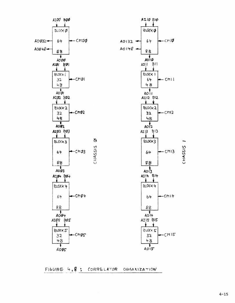
t.pc
32 Cr101
ZLOCK
tfas- CM 1
I+ a
.4—Ct112tt LOCK 2
324-8
ADO/Ax03 1303
raLock31
Lte.
A012
A113 B13
..*--- CN1
cm 13
c64-
1.0C1.< 0
cril0AO 032.-•—
A00 Lfg
6 4
AQA341 BO I
A0132 6 It
AO 14g -6.-
LOCI‹ 3
if Cm 03 (7)
P8—T.- -ADO
Ai 01+ e404
1.0C1.<
6 tt1.0-C tl 4-
RE
AotbitaCts BS'
'eLoo< 5-32 -4-01074-13
Ao OS"
FibUYZE- 4 s CDP.r21..- LA-T-0R op 6A, ivrz ~now
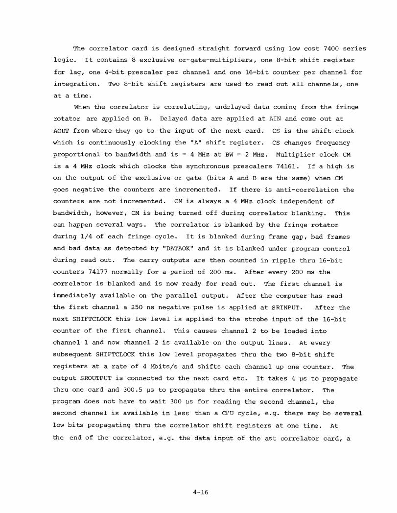
The correlator card is designed straight forward using low cost 7400 series
logic. It contains 8 exclusive or-gate-multipliers, one 8-bit shift register
for lag, one 4-bit prescaler per channel and one 16-bit counter per channel for
integration. Two 8-bit shift registers are used to read out all channels, one
at a time.
When the correlator is correlating, undelayed data coming from the fringe
rotator are applied on B. Delayed data are applied at AIN and come out at
AOUT from where they go to the input of the next card. CS is the shift clock
which is continuously clocking the "A" shift register. CS changes frequency
proportional to bandwidth and is = 4 MHz at BW = 2 MHz. Multiplier clock CM
is a 4 MHz clock which clocks the synchronous prescalers 74161. If a high is
on the output of the exclusive or gate (bits A and B are the same) when CM
goes negative the counters are incremented. If there is anti-correlation the
counters are not incremented. CM is always a 4 MHz clock independent of
bandwidth, however, CM is being turned off during correlator blanking. This
can happen several ways. The correlator is blanked by the fringe rotator
during 1/4 of each fringe cycle. It is blanked during frame gap, bad frames
and bad data as detected by "DATAOK" and it is blanked under program control
during read out. The carry outputs are then counted in ripple thru 16-bit
counters 74177 normally for a period of 200 ms. After every 200 ms the
correlator is blanked and is now ready for read out. The first channel is
immediately available on the parallel output. After the computer has read
the first channel a 250 ns negative pulse is applied at SRINPUT. After the
next SHIFTCLOCK this low level is applied to the strobe input of the 16-bit
counter of the first channel. This causes channel 2 to be loaded into
channel 1 and now channel 2 is available on the output lines. At every
subsequent SHIFTCLOCK this low level propagates thru the two 8-bit shift
registers at a rate of 4 Mbits/s and shifts each channel up one counter. The
output SROUTPUT is connected to the next card etc. It takes 4 ps to propagate
thru one card and 300.5 ps to propagate thru the entire correlator. The
program does not have to wait 300 ps for reading the second channel, the
second channel is available in less than a CPU cycle, e.g. there may be several
low bits propagating thru the correlator shift registers at one time. At
the end of the correlator, e.g. the data input of the ast correlator card, a

terminator is connected which grounds all input lines. As the correlator is
read out "O's" are therefore shifted gradually into all counters and when
all channels have been read the entire correlator is cleared except the
first channel. One more "NXTWRD" command has to be executed to clear the
first channel too. After this there still are several low bits propagating
thru the shift registers for 300 ps and the correlator could not correlate
during that time. This can be reduced to 4 is with a "COR RECOVERY"
command, which applies a low signal at SRSET of all correlator cards in
parallel. It should be noted that while the correlator is read and cleared
the prescalers are not affected. The four least significant bits are not
erased; they are included in the counts during the next 200 ms integration.
The counts of the correlator channels and check channels may differ by one
bit. If a difference of three counts occurs the on-line program causes a
message to be typed and turns off the correlator.
An independent command CORCLR applies a high level at CTRCLR input of
the correlator cards in parallel which clears all counters and prescalers.
It takes 31 ps to execute CORCLR which is followed by correlator recovery
automatically.
Correlator mode multiplexers located on the correlator control board
select A input, B input and multiplier clock of all six blocks and set the
correlator into any one of 8 modes as shown in Figure 1.11.
A second set of multipliers 1F, 1E, 1D, 1C, 1B, 3F, and 3E control the
extra check board with 8 check channels. The check board can be placed in
parallel to any other card in the same chassis under program control. The
check board duplicates exactly all of those 8 channels of correlation and
independently of the type of data correlated should show identical counts.
If a channel is not identical a hardware failure has occurred either in the
particular correlator channel or in the check channel. Note that this works
independently of correlator mode and it works while real data is correlated.
Six control bits CHKBO-5 set the multiplexer. Octal 00 to 43 select
board 00 to 53 as shown in Table 3.7. One additional multiplexer 8A is used
so that the check card can also duplicate all total counts. This happens
for check bits = 70 to 74. A low level is applied at AICHK by gates 8F and
2G and at BICHK by multiplexer 3F and all check channels count clock pulses.
All check channels should have the same count and be equal to the total count.
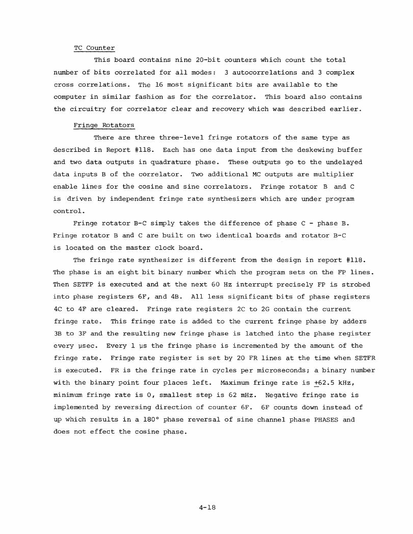
TC Counter
This board contains nine 20-bit counters which count the total
number of bits correlated for all modes: 3 autocorrelations and 3 complex
cross correlations. The 16 most significant bits are available to the
computer in similar fashion as for the correlator. This board also contains
the circuitry for correlator clear and recovery which was described earlier.
Fringe Rotators
There are three three-level fringe rotators of the same type as
described in Report #118. Each has one data input from the deskewing buffer
and two data outputs in quadrature phase. These outputs go to the undelayed
data inputs B of the correlator. Two additional MC outputs are multiplier
enable lines for the cosine and sine correlators. Fringe rotator B and C
is driven by independent fringe rate synthesizers which are under program
control.
Fringe rotator B-C simply takes the difference of phase C - phase B.
Fringe rotator B and C are built on two identical boards and rotator B-C
is located on the master clock board.
The fringe rate synthesizer is different from the design in report #118.
The phase is an eight bit binary number which the program sets on the FP lines.
Then SETFP is executed and at the next 60 Hz interrupt precisely FP is strobed
into phase registers 6F, and 4B. All less significant bits of phase registers
4C to 4F are cleared. Fringe rate registers 2C to 2G contain the current
fringe rate. This fringe rate is added to the current fringe phase by adders
3B to 3F and the resulting new fringe phase is latched into the phase register
every psec. Every 1 ps the fringe phase is incremented by the amount of the
fringe rate. Fringe rate register is set by 20 FR lines at the time when SETFR
is executed. FR is the fringe rate in cycles per microseconds; a binary number
with the binary point four places left. Maximum fringe rate is +62.5 kHz,
minimum fringe rate is 0, smallest step is 62 mHz. Negative fringe rate is
implemented by reversing direction of counter 6F. 6F counts down instead of
up which results in a 180° phase reversal of sine channel phase PHASES and
does not effect the cosine phase.
Buffer Interface This board has most of the receiver-driver circuit to and from the
buffer. Note that CS is the correlator shift clock which changes frequencywith bandwidth. A, B, and C are data outputs to the correlator, FB and FCare data outputs to the fringe rotators and DATA, DATB, and DATC are outputsto a frame count detection circuit on delay display board.
This board also contains an unblanking delay circuit. As soon as
data coming from deskewing buffers is good, DATOK becomes true. However, therestill are invalid data bits in the correlator shift registers. The correlator
has to stay blanked until they are cleared out. The time required is afunction of the mode. Blanking outputs X, Y, and z are delayed according to
the table on the blueprint.
Delay and Fringe Rate Display
The fringe rate is displayed with a five digit LED panel display.
When the fringe rate is >63.5 Hz then HIFR is high and PH7 is counted, which
is the MSS of fringe phase, over a period of I second. The display is in Hz.
If the fringe rate is <63.5 Hz then BTEN is counted which is 10 bits less down
in the fringe phase register. The decimal point is moved three decimals left.
It should be noted that an approximation is made here: 1024 = 1000 and at verylow fringe rates it is possible to rotate the fringe rotator by updating the
phase only; the fringe rate register may well be = 0. The display then may
show 0 where in fact the rotator is rotating slowly.The delay is measured and displayed as difference of 0 frame A and 0 frame
B or C. Zero frame pulses are one pps pulses derived from decoded helicalframe count 0. If data are poor, 0 frame may be decoded improperly and thedisplay will not be stable. It typically jumps around in multiples of 16.6 msor it may not change at all. One should recognize that the display shows the
actual delay between the two data streams and not the delay which the computerhas calculated and thinks it has put into the hardware.
TCD Display and Memoscope Alert
Decoded audio data are converted into parallel format by a 64 bit shiftregister. At the right time when a sync pattern of 111111110000 is recognized,parallel data are latched in a 52 bit latch where they are held for display and
for input to the computer. Every frame the latch is updated. The circuit displays
only one audio channel at a time. With multiplexer 1F any of three recorders
A, B or C may be selected either under computer control when in XFER mode
or by panel switches when in STOP mode. When in XFER mode and the multiplexer
is changed from one recorder to another it will take between 16.6 to 33.2 ms
for new data to be ready. During that time the display is blanked by TCDBLK.
As data is processed and the computer scans thru the recorders rapidly one
cannot read each recorder individually on the display. If one depresses one
of the three select buttons, for example SWA, then during B and C the display
is blanked and A may be read. The display will be dim and will flash because
for over 2/3 of the time it is turned off. A retriggerable one shot circuit
10B detects if any of the 16 ms sync's are missing and turns on TCD error
indicator.
The circuit for ALERT is simple and needs no further explanation. On the same
boardis the circuit to drive the memoscopes. Two D/A converters drive X and Y
respectively of the Tektronix model 603 memoscopes. ZMEM1 and ZMEM2 turn on
the beam currents to plot a point on the screen. Timing is important and needs
to be considered for programming. It takes 15 ps for X and Y to settle for
full scale deflection, and it takes 30 is for Z to plot a point. Erasing a
screen takes 250 ms during which time the scope goes busy. Another control
is DIM which reduces the brightness of the stored image so that it may be
viewed up to 1 hour and life of the CRT is extended. This function is active
only when the brightness control on the front panel is completely counter-
clockwise. Note that the scopes are forced dim when the computer is halted
or when it goes into an unusual mode. COMPRDY and DLYTRK are both missing
then and flip-flops 3G-3F are cleared.
MastercIock
This board contains 6 circuits: Masterclock, correlator-bandwidth
registers, NXTWRD shaper, 60 Hz interrupt, pulsed delay and fringe-rotator
B-C.
The masterclock consists of a 20 MHz crystal oscillator, a divider,
multiplexer and driver circuits. The outputs are:
MCLK: Masterclock 4 MHz squarewave for control circuits within
correlator control chassis.
SHCLK: Shift clock 4 MHz squarewave for correlator read out shift
registers of correlator 0 and 1 respectively.
4-20
SHCLK QT: 1 MHz squarewave for TC counters board
1 MHz: Squarewave for delay display
CM: Multiplier clock 50 ns wide pulse 4 MHz for TC counters
CM0,1: 50 ns 4 MHz pulse for correlator multipliers
CS0,1: Shift clock 50 ns wide for correlator shift registers.
Frequency 4 MHz to 31.25 depending on bandwidth
Multiplier lines CM0 CM1 and shift clock lines CSO and CSI are long twisted
pair lines terminated on both ends by 68Q. This avoids overshoot and controls
transition times accurately throughout the correlator. These lines are driven
by open emitter line driver 8T13.
Next word shaper is a simple circuit which transforms the transmission of
NXTWRD into a 250 ns wide pulse with precise time relation to CM.
60 Hz interrupt circuit has the necessary circuit to interrupt the CPU
and interlock interrupts with DMA transfers. It connects to the computer
via the I/O bus. This 60 Hz interrupt is the only interrupt of the CPU.
Interrupt location is 0 since nothing is connected to the interrupt address
select lines. 60 Hz from buffer sets request flip-flop 3G if interrupt enable
flip-flops 2F8, 2F6 are set. At the next interrupt clock IUCK interrupt flip
flop 3G sets and the CPU gets interrupted by IURX. After this interrupt is
accepted by the CPU IUAX comes back and clears interrupt request flip-flop.
If a DMA request is pending either TPIX or TPDX is low and interrupt flip-
flop is held in the clear state by 3G13. At the next IUCK clock 3G9 will not
be set. Furthermore 8E5 is held low so that request flip-flop 3G5 will not
be cleared. This is necessary because an acknowledge to DMA request appears
on IUAX. After DMA is serviced a waiting interrupt may then be executed at
the next IUCK. Interrupts may be enabled and disabled under program control.
Interrupt enable flip-flop is cleared by IUJX after each interrupt so that no
interrupt is executed twice. The program needs to enable interrupts after
each interrupt. When the computer is halted interrupt enable flip-flop is
also cleared by SYRT when system reset is depressed.
A pulse delay circuit controls delay between tapes A-B and B-C. Every
time RTD or ADV is pulsed by the program a clock pulse is deleted or inserted
at UCLK. The unload counters in the buffers B and C are therefore retarded
by 250 ns per pulse with respect to A. Since 60 Hz reference is derived from
the unload pointer this will actually displace recorder B or C respectively.
Although the advance and retard pulse are executed instantaneously in the
buffer there is a limit how fast the video recorders can be slewed before
head drum servo gets out of lock.
In our experience during the last two years problems and failures
have mostly occurred in the correlator, the decoders, video tape recorders
and computer 9 track tape drive.
Correlator failures are typically in the counters. If a counter counts
improperly then there is a difference between that channel and the corresponding
check dhannel. The program can correctly analyze and find the failing channel.
If a counter fails in a way that parallel loading function of the chip malfunctions,
then other channels than the failing channel are affected. The program will
indicate failure at random channels or will indicate that the terminator is not
zero. Often this happens when a totempole output is damaged so that the output
voltage is between proper TTL levels. This typically causes a high being shifted
into the next counter instead of a low. Note that since clearing the correlator
is done by shifting in all low bits the correlator cannot be cleared. A diagnostic
program READOUT tests whether the correlator shifts properly. Program CORTEST
actually correlates data and compares correlator channels with check channel anddetects errors by halting at particular error locations. Comments at those
locations in the listing help analyze the problems. The sane checking occurs
while actual data is correlated by the on line program system. An error will be
indicated by a TTY message if the difference is larger than two counts.
Failures of the decoder are indicated by various error lights and data cannot
be decoded properly. This happens usually when the phase lock loop is maladjusted,
which retrieves the lock from the BI-0 data. Not only must the phase lock looplock to the input data but the phase must be so that the decoder is able to sample
in the middle of a bit cell. The adjustment of the trimpot capacitor for center
frequency of the PLL is very critical and the circuit is somewhat temperature
dependent. A front panel potentiometer is a fine control for the center frequency.

Failures of the video recorders are mostly not clear cut. Sometimes tape
may work better on one tape recorder than on another. The difference may be
in the video heads or the mechanical alignment or in the response of the
preamplifier. These differences between recorders become less obvious when a
good quality tape with good recording is played back.
Head drum servo and capstan servo are not too well designed. They are
not critically damped. Head drum servo has significant temperature drift.
In general however their performance is good enough for processing tapes
properly. Since report #118 was written major improvements were made in
the stability of the capstan servo and the head drum servo by cleaning up
control track amplifier-clipper and, by closing the head drum servo loopwhich eliminates problems due to temperature drift, and by replacing the
+12 internal supply with a well regulated external supply. Dramatic failures
due to broken video heads, faulty components in the servos, bad switches or
relays are easily spotted and repaired by replacement of a card or component.
Excessive play in worn bearings, etc. can be spotted very easily and needs
to be attended to by an experienced service technician.
The nine track 1/2" tape drive has given us numerous problems. Some
of the gaskets of the vacuum system have failed, causing the vacuum to be
unstable to the extent that tapes could not be loaded. We have had a sizable
number of failures with the Molex connectors which interconnect all boards.
According to Molex these connectors are not made for low voltage, low current
applications as in this tape unit. Another failure we have had was in the
controller timing circuit which sets record gap length. A diagnostic program
"TAPE" checks for proper record gap length as well as proper recording.
Another diagnostic program "MEMO" is used to test the performance of
both D/A converters and to check alignment of the memoscopes. MEMO displays
three different patterns on the screen. A crossed rectangle makes visible
any faulty bit of either one of the D/A converters. A checkerboard pattern
checks for geometric distortion. The third pattern plots a point everywhere
on the screen. Distortions in the floodgun become visible as well as burned
out spot in the phosphor.

FFT Interface
Interface FFT (NOVA 820) to Varian 620
Two general purpose controllers are used to interface the Nova
820 to the Varian 6201 computer. The Varian uses a buffered I/O controller
mode DM 373B with device address 67. The Nova uses a general purpose interface
mode 4040 and data registers mode 4041 with device address code 04 and interrupt
mask bit 4. Each CPU looks to the other as a peripheral. Data transfers are
in the "test and transfer" mode. The Nova 820 may also be operated in the
interrupt mode. No data channels are provided.
Data transfer occurs in parallel over two independent 16 bit data lines.
Transfer may occur simulataneously in both directions. Over the same lines
16 bit command words are transmitted. Handshaking is done on the ready-
acknowledge principle. Five status bits are used by the Varian to transfer
status information to the Nova of which two are not assigned yet. Six
additional status bits are used by the Nova to indicate status to the Varian
of which one is not assigned yet.
Description of Varian Interface
Device Address = 67
OTB 0 to 15: Output of 16 bit parallel data or control
data.
BI 0 to 15: Input of 16 bit parallel data or control
data.
POT 0 = IACK: To be set after either a data or control
word has been read by Varian.
POT 1 = ODRDY: To be set after output data has been placed
on OTB lines.
POT 2 = OCRDY: To be set after output command has been
placed on OTB lines.
POT 3 = STAT 1: Sets spare status bit.
POT 4 = STAT 2: Sets spare status bit.
POT 5 = CLRSTAT: Clears status bit 1 and 2, FFT RESET, ODRDY,
OCRDY, does not clear VARSYRT.
SEN 0 = °ACK: Set after Nova has accepted either a data
or control word. Gets reset after either
ODRDY or OCRDY.
SEN 1 = IDRDY: Set after Nova has place a data word on BI.
Gets reset by IACK, NOVA IORST, NOVA CLR.
SEN 2 = ICRDY: Set after Nova has placed a command word
on BI. Gets reset by IACK, NOVA IORST,
NOVA CLEAR.
SEN 3 = STAT3: Spare status bit. Gets reset by CLRSTAT,
NOVA IORST, NOVA CLEAR. Gets set by NOVA
IOPULSE.
SEN 6 = FFTRESET: Set during Nova power turn on and during
NOVA IDRST instruction and during Nova
console reset. Cleared by CLRSTAT.
SEN 7 = FFTPWRON: Set when power is applied to Nova.
SYRT: Sets VARSYRT status flip-flop when Varian
console master reset is depressed, VARSYRT
is cleared by DATINC, NOVA IORST, NOVA CLEAR.
Description of Nova Interface
Device Address = 04
Device Code = 04
Interrupt Mask Bit = 4
Output data and output command use the same output lines and therefore only
one may occur at a time. DOA sets status flip-flop IDRDY for transfer of
data, DOB sets status flip-flop ICRDY for transfer of command. Register C is
not implemented. IDRDY and ICRDY are reset by Varian IACK, IORST, CLEAR.
Status 3 (not assigned yet) is set by the pulse output (P = 11 bit 8,
9) of control function F. Status 3 is reset by IORST or clear command code
C in F. Status bit FFTWRON is set whenever power is applied to the Nova.
Status bit FFTRESET is set by NOva IORST and is cleared by Varian CLRSTAT.
Input data and input command use the same input lines and therefore only
one may occur at a time. DIA read a data word in and resets IDRDY status
flip-flop. DIB reads a command word in and resets ICRDY status flip-flop. DIC
reads a 5 bit status word in status word format:
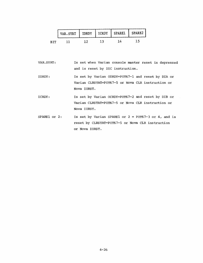
SPARE1 [ SPARE2VAR. SYRT IDRDY ICRDY
BIT 11 12 13 14 15
VAR. SYRT : Is set when Varian console master reset is depressed
and is reset by DIC instruction.
I DRDY :
ICRDY:
SPAREI or 2:
Is set by Varian ODRDY=P0T67-1 and reset by DIA or
Varian CLRSTAT=P0T67-5 or Nova. CLR instruction or
Nova IORST.
Is set by Varian OCRDY=P0T67-2 and reset by DIB or
Varian CLRSTAT=P0T67-5 or Nova CLR instruction or
Nova IORST.
Is set by Varian SPARE1 or 2 = P0T67-3 or 4, and is
reset by CLRSTAT=P0T67-5 or Nova CLR instruction
or Nova IORST.

SEN 67-3
SO1161-7
ett/ 67 -- 6
L Z
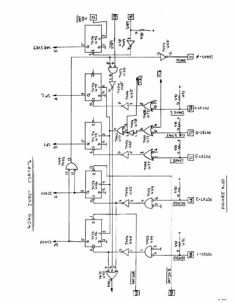
01
•41
32
,m9
id
CO
I01
tak5z I >
.114104.11..*01
E:1-\trz.L
it43
1L
aJLN
OIY
Idt4G
-110 41--4
0--4
z4-1-? -46G
01
E-4-D
.S 1
1
4101.0._-h
q0 411
— —
S9 V
I41 a +,
e
aA
L 11ti.T.4
)La'
/iE
l
to-h
t.n
I
—1
t7N
el
÷ N
M,
601.41
11 NT L
AM
--4A
0
fr
1m
0
0 0
-111
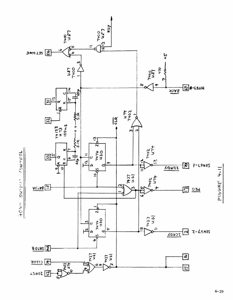
I •4
1 3N
nc)1:-z)
v.)rri
rri
1`)
11.s
ViD
oqn
z .41L+ILso
Ol
AqaL
mv
t Ztzt
ogy\7
sh LAIL s
Ef<
I0041 L.
LrYt
ci
zj)1
1'S
do9
93 av
Ler
00
11 L
01
Ii4:7
(11
-121r-
0
(CT
70
• •■•■•■•••■•■..
rj /4
6 )
;:r1C
)\.)
047
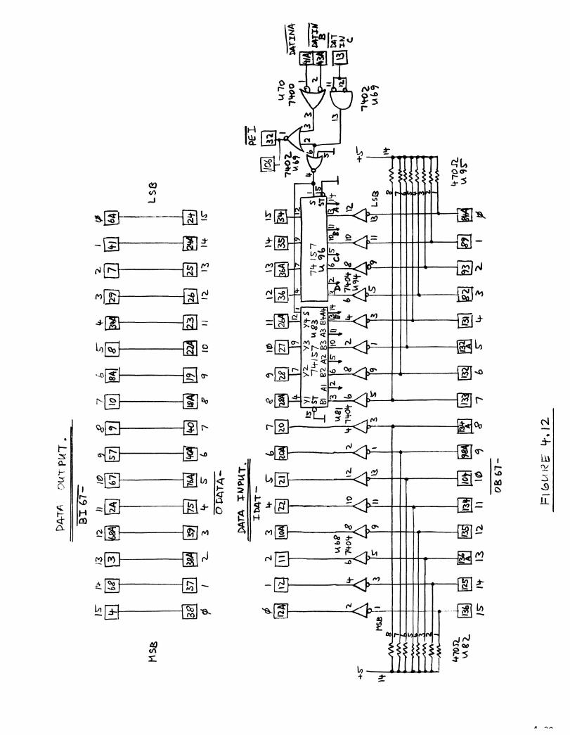
Z1
`41
L9 .80
z6 Y
1"Z
r oL
fq'g
691nV
AL
tut
s
-ki ttrava
oo4a.h
40�438 •-v
.2
zy
Z.Z1 I V
iaE
a 1-1 LS
14
7 Lis
S-6C
FA
-4A
IA•
ii
zi6
Li ell
G 118;
CI] E
lI93
-1 ad
21ivot
9 _5
E
14/4
I/VI
—VIVI 0
.S1
of6
411L
if
eS
18
StV
8 Z
. I01
It
L9 m
e
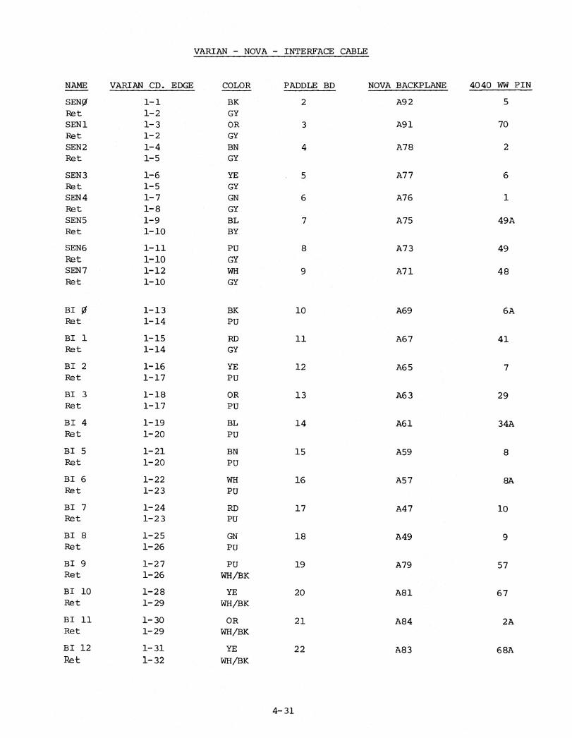
VARIAN - NOVA - INTERFACE CABLE
NAME VARIAN CD. EDGE COLOR PADDLE BD NOVA BACKPLANE 4040 WW PIN
SENY 1-1 BK 2 A92 5Re t 1-2 GYSEN 1 1-3 OR 3 A91 70Re t 1-2 GYSEN2 1-4 BN 4 A78 2Re t 1-5 GY
SEN 3 1-6 YE 5 A77 6Re t 1-5 GYSEN 4 1-7 GN 6 A76 1Re t 1-8 GYSEN5 1-9 BL 7 A75 49ARet 1-10 BY
SEN6 1-11 PU 8 A73 49Ret 1-10 GYSEN 7 1-12 WH 9 A71 48Pet 1-10 GY
BI 0 1-13 BK 10 A69 6ARe t 1-14 PU
BI 1 1-15 RD 11 A67 41Pet 1-14 GY
BI 2 1-16 YE 12 A65 7Re t 1-17 PU
BI 3 1-18 OR 13 A63 29Re t 1-17 PU
BI 4 1-19 BL 14 A61 34ARe t 1-20 PU
BI 5 1-21 BN 15 A59 8Ret 1-20 PU
BI 6 1-22 WH 16 A57Re t 1-23 PU
BI 7 1-24 RD 17 A47 10Re t 1-23 PU
BI 8 1-25 GN 18 A49 9Re t 1-26 PU
BI 9 1-27 PU 19 A79 57Ret 1-26 WH/BK
BI 10 1-28 YE 20 A81 67Re t 1-29 WH/BK
BI 11 1-30 OR 21 A84 2ARet 1-29 WH/BK
BI 12 1-31 YE 22 A83 68ARet 1-32 WH/BK
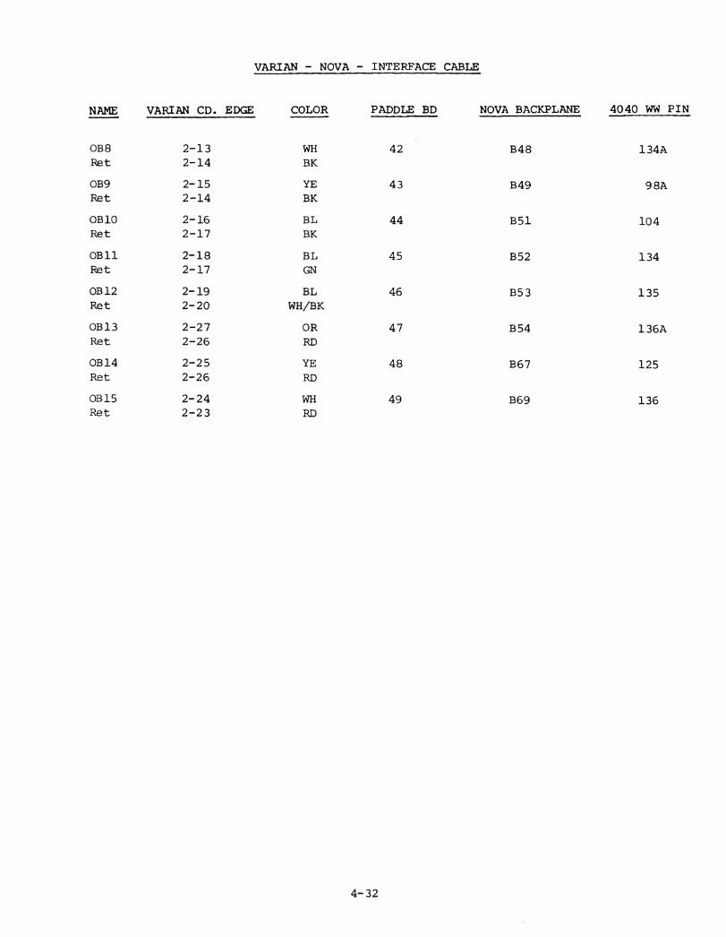
VARIAN - NOVA - INTERFACE CABLE
NAME VARIAN CD. EDGE COLOR PADDLE BD NOVA BACKPLANE 40 40 WW PIN
0B8 2-13 WH 42 B48 134ARet 2-14 BK
0B9 2-15 YE 43 B49 98ARet 2-14 BK
OB10 2-16 BL 44 B51 104Ret 2-17 BK
OB11 2-18 BL 45 B52 134Ret 2-17 GN
0812 2-19 BL 46 B53 135Ret 2-20 WH/BK
0B13 2-27 OR 47 B54 136ARet 2-26 RD
0B14 2-25 YE 48 B67 125Ret 2-26 RD
0B15 2-24 WH 49 B69 136Ret 2-23 RD
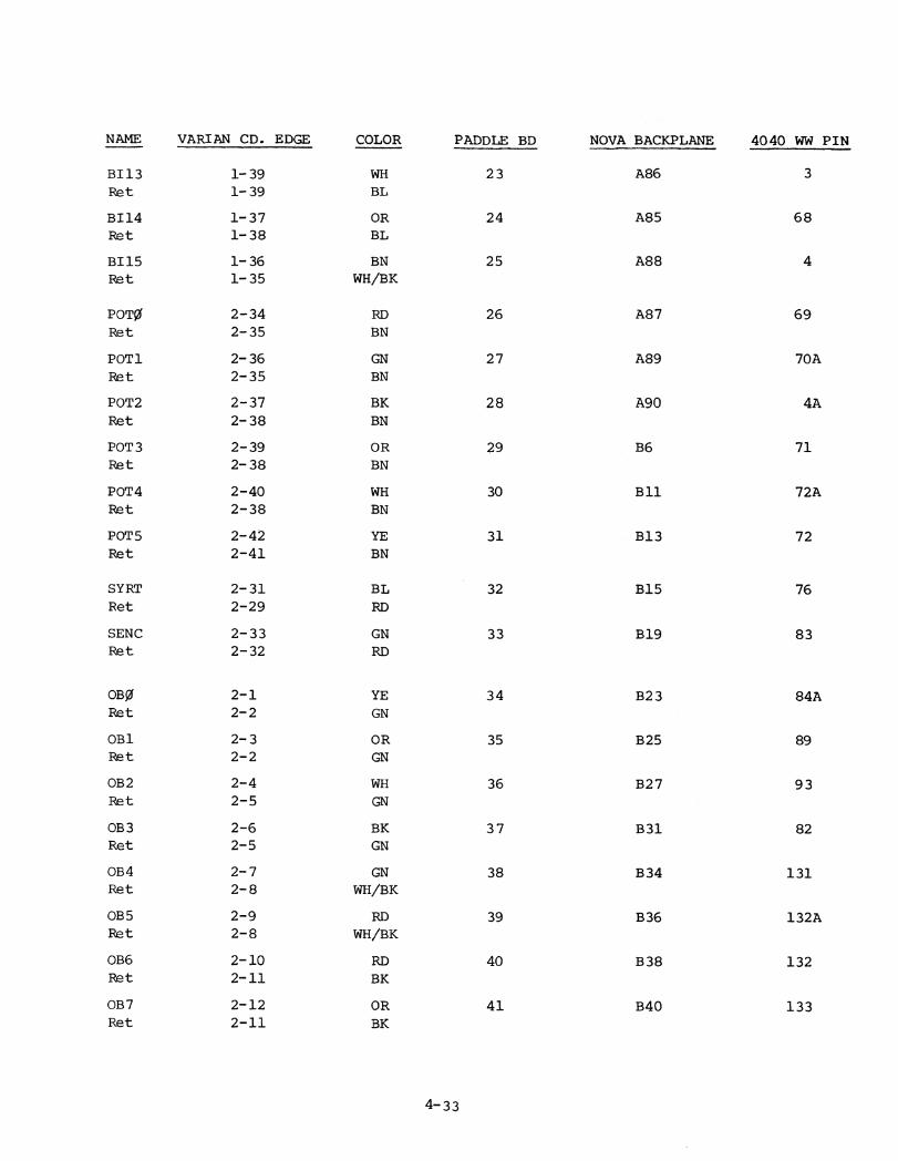
NAME VARIAN CD. EDGE COLOR PADDLE BD NOVA BACKPLANE 4040 WW PIN
BI13 1-39 WH 23 A86 3Ret 1-39 BL
BI14 1-37 OR 24 A85 68Pet 1-38 BL
BI15 1-36 BN 25 A88 4Pet 1-35 WH/BK
POTO 2-34 RD 26 A87 69Pet 2-35 BN
POT1 2-36 GN 27 A89 70ARet 2-35 BN
POT2 2-37 BK 28 A90 4ARet 2-38 EN
POT3 2-39 OR 29 B6 71Ret 2-38 BN
POT4 2-40 WH 30 B11 72ARet 2-38 BN
POT5 2-42 YE 31 B13 72Ret 2-41 EN
SYRT 2-31 BL 32 B15 76Ret 2-29 RD
SENC 2-33 GN 33 B19 83Ret 2-32 RD
OBO 2-1 YE 34 B23 84ARet 2-2 GN
OB1 2-3 OR 35 B25 89Ret 2-2 GN
0B2 2-4 WE 36 B27 93Ret 2-5 GN
0B3 2-6 BK 37 B31 82Ret 2-5 GN
0B4 2-7 GN 38 B34 131Ret 2-8 WH/BK
0B5 2-9 RD 39 B36 132APet 2-8 WH/BK
0B6 2-10 RD 40 B38 132Ret 2-11 BK
0B7 2-12 OR 41 B40 133Ret 2-11 BK
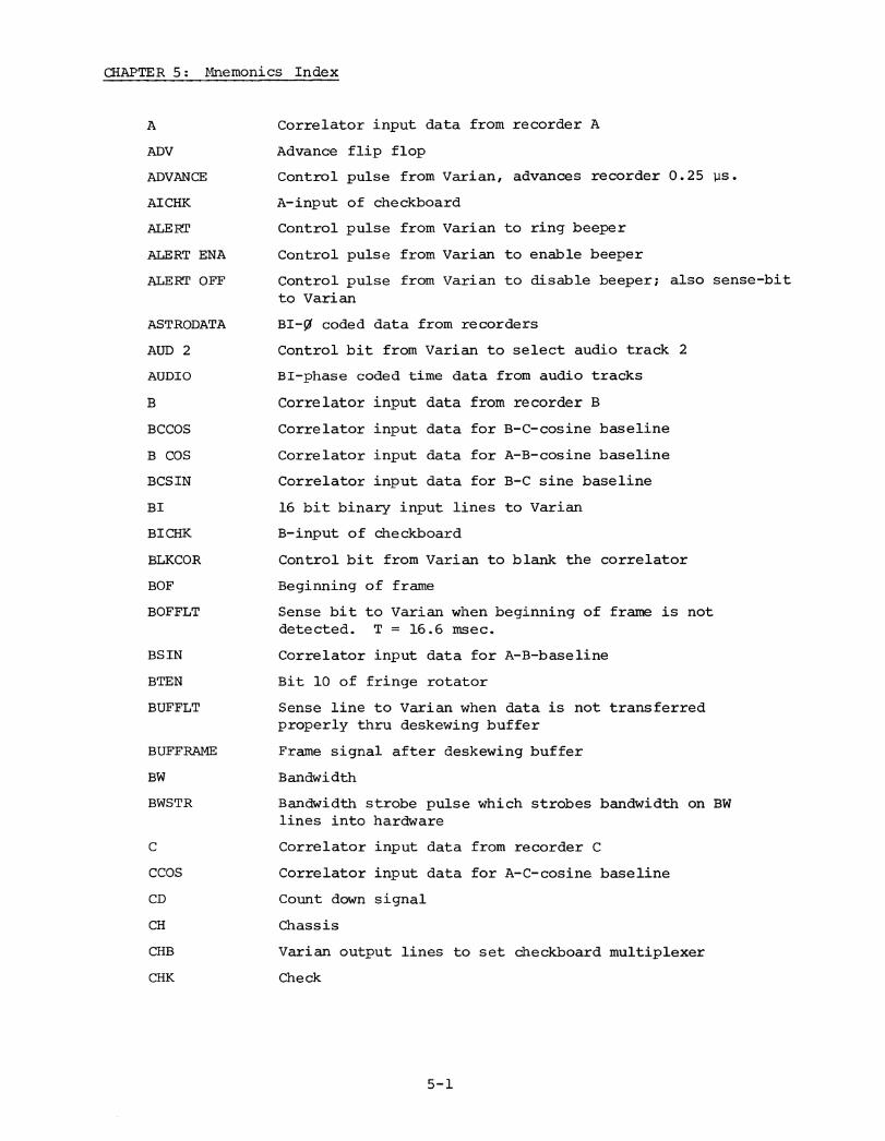
CHAPTER 5: Mnemonics Index
A Correlator input data from recorder A
ADV Advance flip flop
ADVANCE Control pulse from Varian, advances recorder 0.25 ps.
AICHK A-input of checkboard
ALERT Control pulse from Varian to ring beeper
ALERT ENA Control pulse from Varian to enable beeper
ALERT OFF Control pulse from Varian to disable beeper; also sense-bitto Varian
ASTRODATA BI-Y coded data from recorders
AUD 2 Control bit from Varian to select audio track 2
AUDIO BI-phase coded time data from audio tracks
Correlator input data from recorder B
BCCOS Correlator input data for B-C-cosine baseline
B COS Correlator input data for A-B-cosine baseline
BCSIN Correlator input data for B-C sine baseline
BI 16 bit binary input lines to Varian
BICHK B-input of dheckboard
BLKCOR Control bit from Varian to blank the correlator
BOF Beginning of frame
BOFFLT Sense bit to Varian when beginning of frame is notdetected. T = 16.6 nsec.
BSIN Correlator input data for A-B-baseline
BTEN Bit 10 of fringe rotator
BUFFLT Sense line to Varian when data is not transferredproperly thru deskewing buffer
BUFFRAME Frame signal after deskewing buffer
BW Bandwidth
BWSTR Bandwidth strobe pulse which strobes bandwidth on BWlines into hardware
Correlator input data from recorder C
CCOS Correlator input data for A-C-cosine. baseline
CD Count down signal
CH Chassis
CHB Varian output lines to set dheckboard multiplexer
CHK Check

CLRSTAT Control pulse from Varian to clear Nova status flip-flops
CLRXFER Control pulse from Varian to clear transfer flip-flop
CM 4 MHz multiplier clock for TC counters
CM0.1 4 MHz multiplier clock to chassis y and 1
COMPPDY Control pulse from Varian to turn off 'Computer off' light
CORBSY Sense line to Varian, goes true after CORCLR and CORPECOVERYcommand
CORCLR Control pulse from Varian to clear correlator
CORMX Control lines from Varian to set correlator mode
CORMXSTR Control pulse from Varian which strobes correlator modeon CORMX lines into hardware
COROUT 16 parallel output lines from correlator to Varian
CORRECOVERY Control pulse from Varian to recover correlator fornext correlation after all channels are read
CORTEST Diagnostic correlator test program
CPU Central Processor Unit
CRT Cathode ray tube
CS Shift clock
CS0,1 Shift clock to chassis 0 or 1
CSIN Correlator input data for A-C sine baseline
CTRCLR Counter clear input of correlator card
CU Count up
DAT 16 bit correlator output data
DATOK Correlator input flag, true when data has no errors
DELAY Varian output lines to set Monostore delay
DELAYTRACK Control pulse from Varian to clear 'Computer off' light
DELCT Hardware counter to keep track of frame cycle 0-1-2-3-4-0
DELCYC Hardware delay cycle flip flop is set during time whennew delay is set
DELSTR Control pulse from Varian to strobe a new DEL into thehardware
DIM Signal to Memoscope to dim the screen
DIMMEMO Control pulse from Varian to dim Memos copes
DIMPESET Control pulse from Varian to brighten Memoscope
DMA Direct memory access
DROPOUT Sense line to Varian, set when error in data has occurred
DSPTC Input line to Varian, panel time constant switch
EOF End of frame
EXC External control, control pulse from Varian
FB Undelayed data B
FC Undelayed data C
FCT Delayed frame signal
FFTRESET Sense line to Varian, true when Nova is reset
FFTPWRON Sense line to Varian, true when Nova power is on
FLERR Frame lenght error, turns on dropout light
FP Fringe phase
FPB Varian output lines for fringe phase B
FPC Varian output lines for fringe phase C
FR Varian output lines for fringe rate
FRAME Frame signal as decoded off the tape
FRM Frame signal delayed by buffer
HD Input to Varian, hundred daysHEADDRUM DC signal to control phase of recorder head drum servo
HEADSWITCH 30 Hz signal from recorder tachometer
HFC Input line to Varian, helical frame count
HFCOK Input line to Varian, true when helical framecount parity is decoded properly
HIFR Line for fringe rate display, true if rate >62 Hz
HZ Hertz (cycles per second)
IACK Control pulse from Varian to Nova after Varian hasaccepted data from Nova
ICRDY Variansense line, true when Nova has sent a control word
IDRDY Variansense line, true when Nova has sent a data word
INTRPT ENABLE Control pulse from Varian to enable interrupt logic
INTRPT DISABLE Control pulse from Varian to disable interrupt logic
IVC International Video Corp.
IUAX Varian I/O bus line, interrupt acknowledge
IUJX Varian I/O bus line, interrupt jump
IUCX Varian I/O bus line, interrupt clock
IURX Varian I/O bus line, interrupt request
LED Light emitting diode
LDUP Load unload pointer
LP Load pointer

MA Monostore address lines
MCA Multiplier clock for autocorrelator A
MCB Multiplier clock for autocorrelator B
MCBC Multiplier clock for A-B-cosine baseline
MCBS Multiplier clock for A-B-sine baseline
MCC Multiplier clock for autocorrelator C
MCCBC Multiplier clock for C-B-cosine baseline
MCCBS Multiplier clock for C-B-sine baseline
MCCC Multiplier clock for A-C-cosine baseline
MCCS Multiplier clock for A-C-sine baseline
MCLK Master clock
MDO Monostore data out
MEMOBSY Sense line to Varian, true when Memoscope is busy
MEMOCLR Control pulse from Varian, erases screen of Memoscope
MEMOSTR Control pulse from Varian, turns on Memoscope beam toplot a point
MEMOX (Y) Varian output lines to set Memoscope beam
MKIIC Input line to Varian, set when IVC tapes are played
MODE2 Correlator mode 2 line
MRC Monostore read command
MSB Most significant bit
MWC Monostore write command
NEGFR Varian output line for negative fringe rate
NOOP No operation
NEXTWRD Control pulse from Varian, places the next word fromcorrelator on COROUT lines
OACK Sense line to Varian, set after Nova has accepted aword from Varian
OCRDY Control pulse from Varian, tells Nova that Varian hassent a control word
ODRDY Control pulse from Varian, tells Nova that Varian hassent a data word
OVFLO Overflow flip flop of adder
OTB Varian output bit
P117 Most significant bit of fringe phase
PLL Phase lock loop

READOUT Diagnostic program
REFCLK 4 MHz reference clock to buffer
REFUP Reference unload pointer
RESET ERROR Control pulse from Varian, resets dropout
RETARD Control pulse from Varian, retards recorder by250 nsec.
RDFAIL Read-fail line, set when a hardware read error isdetected
RDREQ Read request line
RTD Retard flip flop
RUN Varian output line, turns on recorder
RUNSTR Control pulse from Varian, strobes RUN into hardware
SC Shift cicok, see page 4-20
SELHFC Control pulse from Varian, sets HFC multiplexer
SELTCD Control pulse from Varian, sets TCD multiplexer
SEN Varian sense lines
SETFP Control pulse from Varian, strobes FP into hardware
SETFR Control pulse from Varian, strobes FR into hardware
SETSTAT1,2 Control pulse from Varian, sets status flip-flop in Nova
SETWRREQ Set write request line
SETXFER Control pulse from Varian, sets correlator into transfermode
SHCLK 4 MHz shift clock for readout of correlator
SHCLKQT 1 MHz clock for TC counter board
SHF Short frame signal
SKPFRM Skip frame
SLEW Varian output lines to slew recorders
SLEWBSY Varian sense line, true when recorders are slewing
SRDREQ Set read request
SREFUPST Set reference unload pointer in start mode
SRINPUT Shift input of correlator to read out correlator
SROUTPUT Shift output of correlator to read out correlator
STAT3 Varian sense line, senses Nova status 3 flip-flop
STOP Varian sense line for stop button
SW Switch
SYNCADD Address lines for dropout sync
SYRT System reset
S1-8 8 states during which new delay is strobed into hardware
TAPE Diagnostic program
TC Total count
TCAUTO Total count of autocorrelator
TCCROSS Total count of cross correlator
TCD Time coded decimal
TCD BLK Time code blank to blank display
TCD CLK Time code clock
TCD DAT Time code data
TD Input to Varian, ten day
TH Input to Varian, ten hour
TM Input to Varian, ten minutes
TOTEMPOLE Push-pull output stage
TPIX Varian I/O bus line, trap input
TPDX Varian I/O bus line, trap output
TS Input to Varian, ten second
TTY Teletype
UCLK Unload clock
UD Input to Varian, unit day
UH Input to Varian, unit hour
UM Input to Varian, unit minutes
UP Input to Varian, unit total power
US Input to Varian, unit seconds
UT Input to Varian, unit terminal I.D.
VALMA Valid monostore memory address
VALFR Valid frame
VALSYNC Valid dropout sync
VR Video recorder
W0,1 Data to be written into sync memory
WRFAIL Write fail line, set when a hardware write error isdetected
WRREQ Write request
WSAD Write sync at this address
X Analog signal to Memoscope for x-deflection
XFER Sense line to Varian, transfer
Analog signal to Memoscope for Y-deflection
ZMEM Signal to Memoscope to turn on beam
1MHZ 1 MHz squareware for delay display
60 HZ REFERENCE Reference signal to video recorders
60 HZ REF Internal 60 Hz signal
60 HZ Internal 60 Hz signal
EFLT Adder fault, set when hardware does not work properlyduring DELCYC


