DATA SHEETwww.onsemi.com
© Semiconductor Components Industries, LLC, 2014
January, 2022 − Rev. 31 Publication Order Number:
N34TS108/D
Low‐Voltage DigitalTemperature Sensor
N34TS108Description
N34TS108 is a digital-output temperature sensor with adynamically-programmable limit window, and under- and overtemperature alert functions. These features provide optimizedtemperature control without the need of frequent temperature readingsby the controller or application processor.
The N34TS108 features SMBus� and two-wire interfacecompatibility, and allows up to three devices on one bus with theSMBus alert function.
The N34TS108 is ideal for thermal management optimization ina variety of consumer, computer, and environmental applications. Thedevice is specified over a temperature range of –40°C to +125°C.
Features• Dynamically-Programmable Limit Window with Under- and Over
Temperature Alerts• Accuracy:
♦ ±0.75°C (max) from –20°C to +85°C♦ ±1°C (max) from –40°C to +125°C
• Low Quiescent Current:♦ 6 �A Active from –40°C to +125°C
• Supply Range: 1.4 V to 3.6 V
• Resolution: 12 Bits (0.0625°C)
• Package: 1.2-mm × 0.8 mm, 6-Ball WCSP 2.0-mm × 2.0 mm, UDFN6
Typical Applications• Smartphone and Tablet Thermal Management
• Battery Management
• Thermostat Control
• Under- and Over Temperature Protection for EnvironmentalMonitoring and HVAC
Table 1. ABSOLUTE MAXIMUM RATINGS
Parameter Rating Unit
Supply Voltage 3.6 V
Input Voltage −0.5 to 3.6 V
Operating Temperature −55 to 150 °C
Junction Temperature (TJ) 150 °C
Storage Temperature (Tstg) −60 to 150 °C
Stresses exceeding those listed in the Maximum Ratings table may damage thedevice. If any of these limits are exceeded, device functionality should not beassumed, damage may occur and reliability may be affected.
WLCSP6C6 SUFFIX
CASE 567YQ
See detailed ordering and shipping information on page 13 ofthis data sheet.
ORDERING INFORMATION
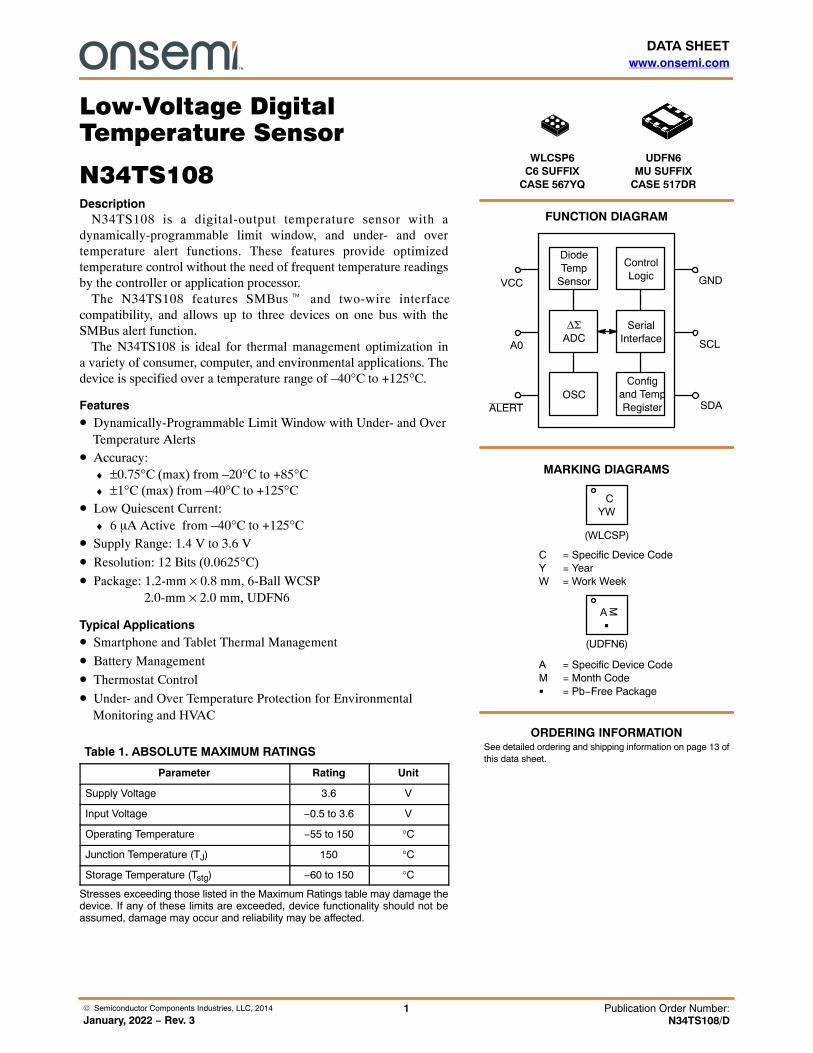
FUNCTION DIAGRAM
SDAALERT
SCL
GND
A0
VCC
ControlLogic
SerialInterface
Configand TempRegister
DiodeTemp
Sensor
��
ADC
OSC
C = Specific Device CodeY = YearW = Work Week
CYW
MARKING DIAGRAMS
(WLCSP)
UDFN6MU SUFFIX
CASE 517DR
A = Specific Device CodeM = Month Code� = Pb−Free Package
A �
(UDFN6)
M
N34TS108
www.onsemi.com2
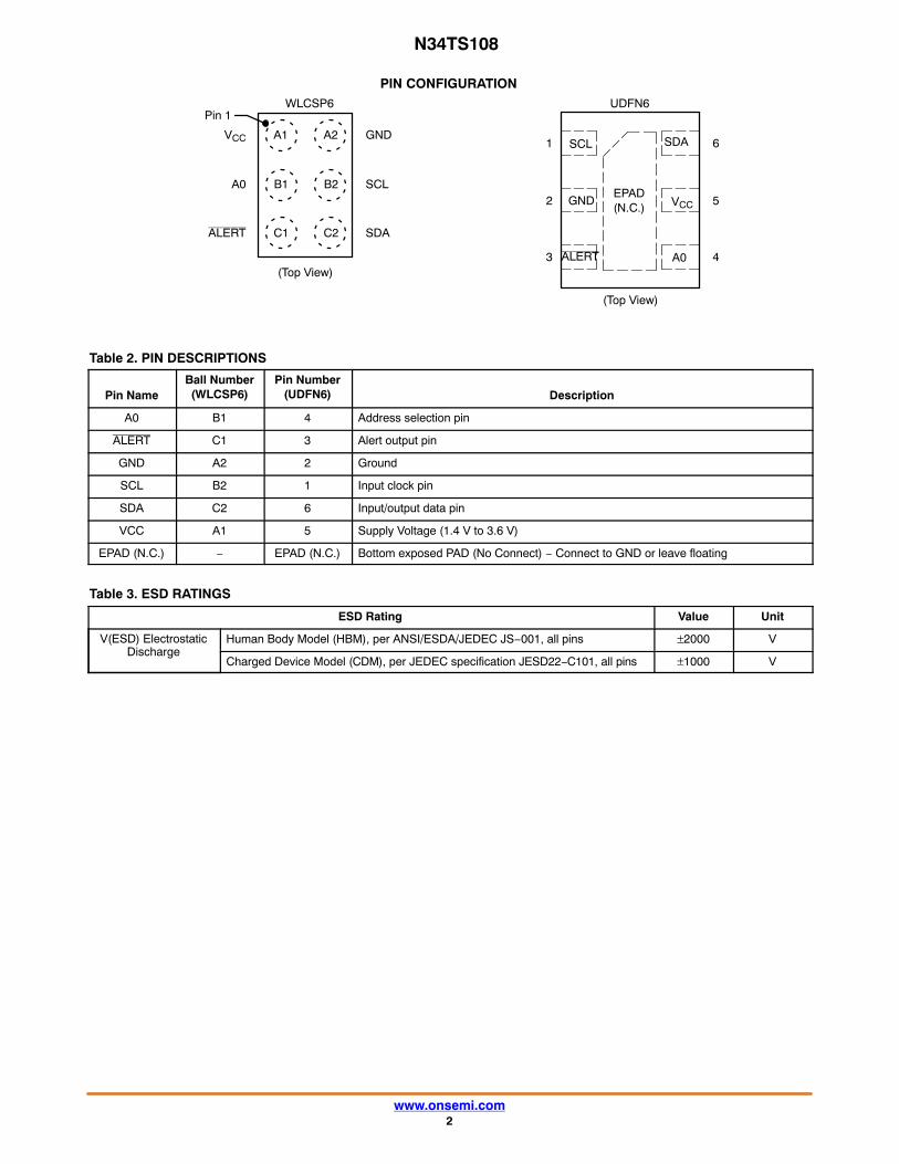
PIN CONFIGURATION
A1 A2
B1 B2
C1 C2
GND
SCL
SDA
VCC
A0
ALERT
(Top View)
Pin 1
VCC
SCL
GND
ALERT
SDA
A0
(Top View)
UDFN6WLCSP6
1
2
3
6
5
4
EPAD(N.C.)
Table 2. PIN DESCRIPTIONS
Pin NameBall Number(WLCSP6)
Pin Number(UDFN6) Description
A0 B1 4 Address selection pin
ALERT C1 3 Alert output pin
GND A2 2 Ground
SCL B2 1 Input clock pin
SDA C2 6 Input/output data pin
VCC A1 5 Supply Voltage (1.4 V to 3.6 V)
EPAD (N.C.) − EPAD (N.C.) Bottom exposed PAD (No Connect) − Connect to GND or leave floating
Table 3. ESD RATINGS
ESD Rating Value Unit
V(ESD) ElectrostaticDischarge
Human Body Model (HBM), per ANSI/ESDA/JEDEC JS−001, all pins ±2000 V
Charged Device Model (CDM), per JEDEC specification JESD22−C101, all pins ±1000 V
N34TS108
www.onsemi.com3
Table 4. D.C. OPERATING CHARACTERISTICS (VCC = 1.8 V, TA = 25°C, unless otherwise specified)
Parameter Conditions Min Typ Max Unit
TEMPERATURE INPUT
Range –40 +125 °C
Accuracy (Temperature Error) –20°C to +85°C ±0.15 ±0.75 °C
–40°C to +125°C ±0.3 ±1 °C
Accuracy vs. Supply ±0.03 ±0.3 °C/V
DIGITAL INPUT/OUTPUT
VIH Input Logic High Level 0.7 (VCC) VCC V
VIL Input Logic Low Level −0.5 0.3 (VCC) V
IIN Input Current 0 V < VIN < (VCC) +0.3 V 1 �A
VOL Output Logic Low Level VCC > 2 V, IOUT = 3 mA 0.4 V
VCC < 2 V, IOUT = 3 mA 0.2 (VCC) V
ALERT Internal Pull-up Resistor ALERT to VCC 80 100 120 k�
Resolution 12 Bit
Conversion Time One-Shot mode 17 22 28 ms
Conversion Modes CR1 = 0, CR0 = 0 0.25 Conv/s
CR1 = 0, CR0 = 1 (default) 1 Conv/s
CR1 = 1, CR0 = 0 4 Conv/s
CR1 = 1, CR0 = 1 16 Conv/s
Timeout Time 21 30 35 ms
POWER SUPPLY
Operating Supply Range, VCC Pin
1.4 3.6 V
IQ Quiescent Current Serial bus inactive, CR1 = 0, CR0 = 1 (default) 3.1 3.6 �A
Serial bus inactive, CR1 = 0, CR0 = 1 (default), –40°C to +125°C
6 �A
Serial bus active, SCL frequency = 400 kHz, CR1 = 0, CR0 = 1 (default)
8 �A
Serial bus active, SCL frequency = 3.4 MHz, CR1 = 0, CR0 = 1 (default)
41 �A
ISD Shutdown Current Serial bus inactive 2.5 3.1 �A
Serial bus active, SCL frequency = 400 kHz 8 �A
Serial bus active, SCL frequency = 3.4 MHz 41 �A
TEMPERATURE
Specified Range –40 +125 °C
Storage Range –55 +150 °C
N34TS108
www.onsemi.com4
Table 5. A.C. OPERATING CHARACTERISTICS (VCC = 1.4 V to 3.6 V, TA = −40°C to +125°C)
Parameter Test Conditions
Fast Mode High Speed Mode
UnitMin Max Min Max
f(SCL) SCL Operating Frequency, VCC ≥ 1.8 V 0.001 0.4 0.001 3.4 MHz
SCL Operating Frequency, VCC < 1.8 V 0.001 0.4 0.001 2.5 MHz
t(BUF) Bus Free Time between Stop and Start Conditions, VCC ≥ 1.8 V
1300 160 ns
Bus Free Time between Stop and Start Conditions, VCC < 1.8 V
1300 260 ns
t(HDSTA) Hold Time after Repeated Start Condition. After this period, the first clock is generated.
600 160 ns
t(SUSTA) Repeated Start Condition Setup Time 600 160 ns
t(SUSTO) Stop Condition Setup Time 600 160 ns
t(HDDAT) Data Hold Time, VCC ≥ 1.8 V 0 900 0 70 ns
Data Hold Time, VCC < 1.8 V 0 900 0 130 ns
t(SUDAT) Data Setup Time, VCC ≥ 1.8 V 100 10 ns
Data Setup Time, VCC < 1.8 V 100 50 ns
t(LOW) SCL Clock Low Period, VCC ≥ 1.8 V 1300 160 ns
SCL Clock Low Period, VCC < 1.8 V 1300 260 ns
t(HIGH) SCL Clock High Period 600 60 ns
tR, tF − SDA Data Rise/Fall Time 300 80 ns
tR, tF − SCL Clock Rise/Fall Time 300 40 ns
tR Clock/Data Rise Time for SCLK ≤ 100 kHz 1000 ns
1. For the N34TS108, the interface will reset itself and will release the SDA line if the SCL line stays low beyond the tTIMEOUT limit. The time-outcount takes place when SCL is low in the time interval between START and STOP.
2. In a “Wired-OR” system (such as I2C or SMBus), SDA rise time is determined by bus loading. Since each bus pull-down device must be ableto sink the (external) bus pull-up current (in order to meet the VIL and/or VOL limits), it follows that SDA fall time is inherently faster than SDArise time. SDA rise time can exceed the standard recommended tR limit, as long as it does not exceed tLOW − tDH − tSU:DAT, where tLOW andtDH are actual values (rather than spec limits). A shorter tDH leaves more room for a longer SDA tR, allowing for a more capacitive bus ora larger bus pull-up resistor.
3. The first valid temperature recording can be expected after tPU at nominal supply voltage.
Table 6. PIN CAPACITANCE (VCC = 3.6 V, TA = 25°C, f = 400 kHz)
Symbol Parameter Test Conditions/Comments Min Max Unit
CIN SDA, Pin Capacitance VIN = 0 8 pF
Input Capacitance (SCL) VIN = 0 6 pF
N34TS108
www.onsemi.com5
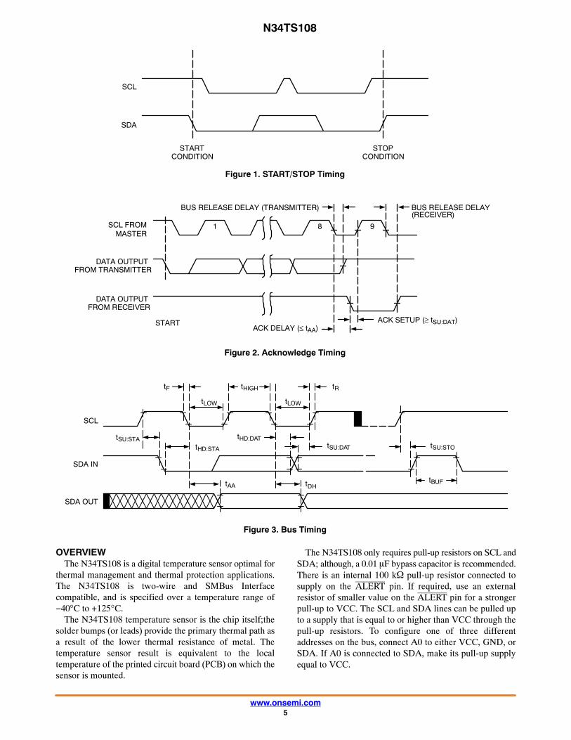
Figure 1. START/STOP Timing
SCL
SDA
STARTCONDITION
STOPCONDITION
Figure 2. Acknowledge Timing
BUS RELEASE DELAY (TRANSMITTER) BUS RELEASE DELAY
SCL FROMMASTER
1 8 9
DATA OUTPUTFROM TRANSMITTER
DATA OUTPUTFROM RECEIVER
STARTACK DELAY (≤ tAA)
ACK SETUP (≥ tSU:DAT)
(RECEIVER)
Figure 3. Bus Timing
tF
tLOW
tHIGH tR
tLOW
SCL
tSU:STAtHD:STA
tHD:DATtSU:DAT tSU:STO
SDA IN
SDA OUT
tAA tDHtBUF
OVERVIEWThe N34TS108 is a digital temperature sensor optimal for
thermal management and thermal protection applications.The N34TS108 is two-wire and SMBus Interfacecompatible, and is specified over a temperature range of−40°C to +125°C.
The N34TS108 temperature sensor is the chip itself;thesolder bumps (or leads) provide the primary thermal path asa result of the lower thermal resistance of metal. Thetemperature sensor result is equivalent to the localtemperature of the printed circuit board (PCB) on which thesensor is mounted.
The N34TS108 only requires pull-up resistors on SCL andSDA; although, a 0.01 �F bypass capacitor is recommended.There is an internal 100 k� pull-up resistor connected tosupply on the ALERT pin. If required, use an externalresistor of smaller value on the ALERT pin for a strongerpull-up to VCC. The SCL and SDA lines can be pulled upto a supply that is equal to or higher than VCC through thepull-up resistors. To configure one of three differentaddresses on the bus, connect A0 to either VCC, GND, orSDA. If A0 is connected to SDA, make its pull-up supplyequal to VCC.
N34TS108
www.onsemi.com6
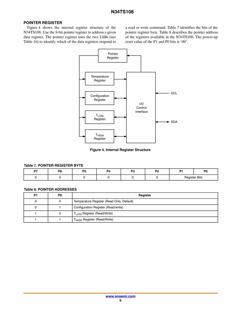
POINTER REGISTERFigure 4 shows the internal register structure of the
N34TS108. Use the 8-bit pointer register to address a givendata register. The pointer register uses the two LSBs (seeTable 16) to identify which of the data registers respond to
a read or write command. Table 7 identifies the bits of thepointer register byte. Table 8 describes the pointer addressof the registers available in the N34TS108. The power-upreset value of the P1 and P0 bits is ‘00’.
Figure 4. Internal Register Structure
PointerRegister
TemperatureRegister
ConfigurationRegister
TLOWRegister
THIGHRegister
I/OControl
Interface
SCL
SDA
Table 7. POINTER REGISTER BYTE
P7 P6 P5 P4 P3 P2 P1 P0
0 0 0 0 0 0 Register Bits
Table 8. POINTER ADDRESSES
P1 P0 Register
0 0 Temperature Register (Read Only, Default)
0 1 Configuration Register (Read/write)
1 0 TLOW Register (Read/Write)
1 1 THIGH Register (Read/Write)
N34TS108
www.onsemi.com7
TEMPERATURE REGISTERThe temperature register is configured as a 12-bit,
read-only register that stores the output of the most recentconversion. Two bytes must be read to obtain data, as shownin Table 9 and Table 10. Note that byte 1 is the mostsignificant byte, followed by byte 2, the least significantbyte. The first 12 bits are used to indicate temperature. Thereis no requirement to read the least significant byte if that
information is not needed (for example, for resolution lowerthan 1°C). Table 11 summarizes the temperature dataformat. One LSB equals 0.0625°C. Negative numbers arerepresented in binary twos complement format. Followingpower-up or reset, the temperature register reads 0°C untilthe first conversion is complete. The unused bits in thetemperature register always read ‘0’.
Table 9. BYTE 1 OF TEMPERATURE REGISTER
D7 D6 D5 D4 D3 D2 D1 D0
T11 T10 T9 T8 T7 T6 T5 T4
Table 10. BYTE 2 OF TEMPERATURE REGISTER
D7 D6 D5 D4 D3 D2 D1 D0
T3 T2 T1 T0 0 0 0 0
Table 11. TEMPERATURE DATA FORMAT (Note 4)
Temperature (�C)
Digital Output
Binary Hex
128 0111 1111 1111 7FF
127.9375 0111 1111 1111 7FF
100 0110 0100 0000 640
80 0101 0000 0000 500
75 0100 1011 0000 4B0
50 0011 0010 0000 320
25 0001 1001 0000 190
0.25 0000 0000 0100 004
0 0000 0000 0000 000
–0.25 1111 1111 1100 FFC
–25 1110 0111 0000 E70
–55 1100 1001 0000 C90
4. The temperature sensor ADC resolution is 0.0625°C/count.
Table 11 does not supply a full list of all temperatures. Usethe following rules to obtain the digital data format fora given temperature.• To convert positive temperatures to a digital data
format:Divide the temperature by the resolution. Then, convertthe result to binary code with a 12-bit, left-justifiedformat, and MSB = 0 to denote a positive sign.Example: (+50°C)/(0.0625°C/count) = 800 = 320h =0011 0010 0000
• To convert negative temperatures to a digital dataformat:Divide the absolute value of the temperature by theresolution, and convert the result to binary code with a 12-bit, left-justified format. Then, generate the twoscomplement of the result by complementing the binarynumber and adding one. Denote a negative number withMSB = 1.Example: (|–25°C|)/(0.0625°C/count) = 400 = 190h =0001 1001 0000Twos complement format: 1110 0110 1111 + 1 = 11100111 0000
N34TS108
www.onsemi.com8
CONFIGURATION REGISTERThe configuration register is a 16-bit read and write
register used to store bits that control the operational modesof the temperature sensor. Read and write operations are
performed MSB first. The format and power-up (reset)default value of the configuration register is shown inTable 12, followed by an explanation of the register bits.Other options for the default values are available by request.
Table 12. CONFIGURATION AND POWER-UP/RESET FORMAT
Byte D7 D6 D5 D4 D3 D2 D1 D0
1 ID CR1 CR0 FH FL TM M1 M0
0 0 1 0 0 1 1 0
2 POL 0 HYS1 HYS0 0 0 0 0
0 0 0 1 0 0 0 0
Hysteresis Control (HYS1 and HYS0)When operating in comparator mode, the hysteresis
control bits (HYS1 and HYS0) configure the hysteresis for
the limit comparison of the N34TS108 to 0°C, 1°C, 2°C, or4°C. The default hysteresis is 1°C. Table 13 shows thesettings for HYS1 and HYS0.
Table 13. HYSTERESIS SETTINGS
HYS1 HYS2 Hysteresis
0 0 0°C
0 1 1°C (Default)
1 0 2°C
1 1 4°C
Polarity (POL)The polarity of the ALERT pin can be programmed using
the POL bit. If POL = ‘0’ (default), the ALERT is active low.For POL = ‘1’, the ALERT pin is active high, and the stateof the ALERT pin is inverted.
Mode Bits (M1 and M0)The mode bits, M1 and M0, can be set to three different
modes: shutdown, one-shot, or continuous conversion.
Shutdown Mode (M1 = ‘0’, M0 = ‘0’)Shutdown mode saves power by shutting down all device
circuitry other than the serial interface, thus reducing currentconsumption to typically less than 2.5 �A. Shutdown modeis enabled when M1 and M0 = ‘00’. The device shuts downwhen current conversion is completed.
One-Shot Mode (M1 = ‘0’, M0 = ‘1’)The N34TS108 features a one-shot temperature
measurement mode. When the device is in shutdown mode,writing a ‘01’ to the M1 and M0 bits starts a singletemperature conversion. During the conversion, the M1 andM0 bits reads ‘01’. The device returns to the shutdown stateat the completion of the single conversion. After theconversion, the M1 and M0 bits read ‘00’. This feature is
useful for reducing the power consumption of theN34TS108 when continuous temperature monitoring is notrequired.
As a result of the short conversion time, the N34TS108can achieve a higher conversion rate. A single conversiontypically takes 22 ms and a read can take place in less than20 �s. However, when using one-shot mode, 30 or moreconversions per second are possible.
Continuous Conversion Mode (M1 = ‘1’)When the N34TS108 is in continuous conversion mode
(M1 = ‘1’), a single conversion is performed at a ratedetermined by the conversion rate bits (CR1 and CR0 in theconfiguration register). The N34TS108 performs a singleconversion, and then goes in standby and waits for theappropriate delay set by the CR1 and CR0 bits. See Table 14for CR1 and CR0 settings.
Thermostat Mode (TM)The thermostat mode bit indicates to the device whether
to operate in comparator mode (TM = ‘0’) or interrupt mode(TM = ‘1’, default). For more information on comparatorand interrupt modes, see the High- and Low-Limit Registerssection.
N34TS108
www.onsemi.com9
Temperature Watchdog Flags (FL and FH)The N34TS108 uses temperature watchdog flags in the
configuration register that indicate the result of comparingthe device temperature at the end of every conversion to thevalues stored in the temperature limit registers (THIGH andTLOW). If the temperature of the N34TS108 exceeds thevalue in the THIGH register, then the flag-high bit (FH) in theconfiguration register is set to ‘1’. If the temperature fallsbelow the value in the TLOW register, then the flag-low bit(FL) is set to ‘1’. If both flag bits remain ‘0’, then thetemperature is within the temperature range set by thetemperature limit registers. In interrupt mode, when any ofthe flags is set by an under- or over-temperature event, the
SMBus ALERT Response only clears the pin and not theflags. Reading the configuration register clears both theflags and the pin unless the device is in comparator mode.
Conversion RateThe conversion rate bits, CR1 and CR0, configure the
N34TS108 for conversion rates of 0.25 Hz, 1 Hz, 4 Hz, or16 Hz. The default rate is 1 Hz. The N34TS108 has a typicalconversion time of 22 ms. To achieve different conversionrates, the N34TS108 makes a conversion, and then powersdown and waits for the appropriate delay set by CR1 andCR0. Table 14 shows the settings for CR1 and CR0.
Table 14. CONVERSION RATE SETTINGS
CR1 CR0 Conversion Rate IQ (Typ)
0 0 0.25 Hz 3 �A
0 1 1 Hz (Default) 4 �A
1 0 4 Hz 5 �A
1 1 16 Hz 13 �A
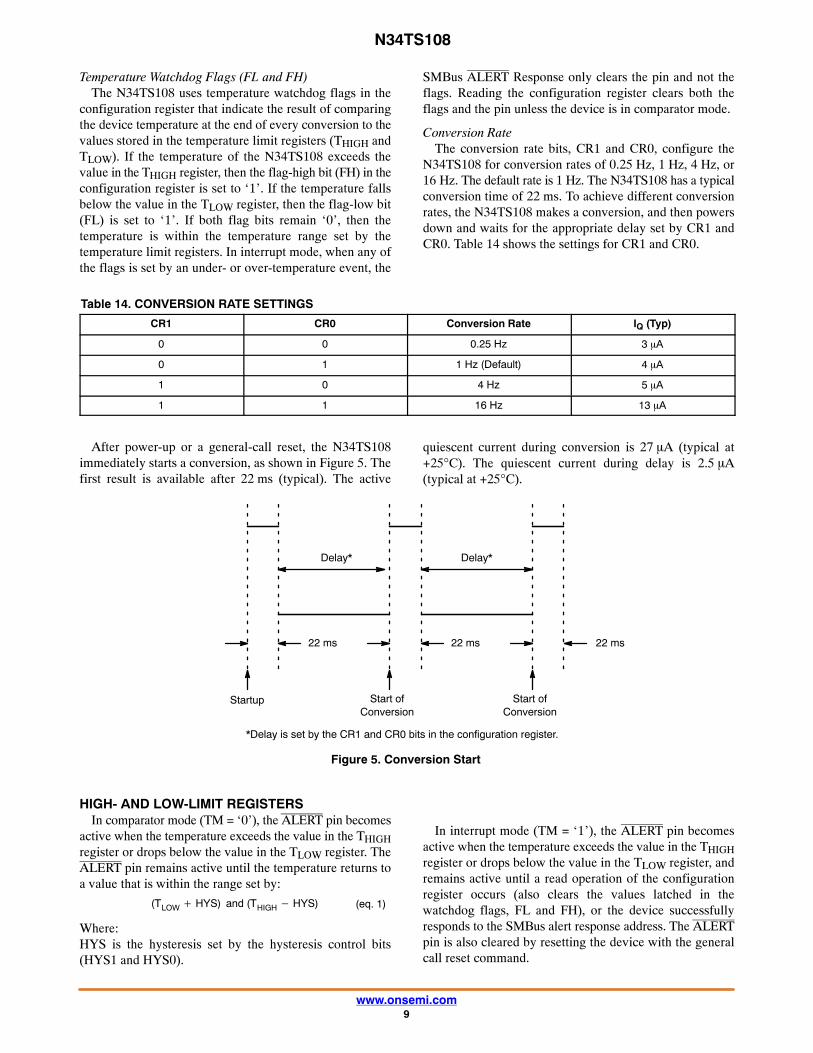
After power-up or a general-call reset, the N34TS108immediately starts a conversion, as shown in Figure 5. Thefirst result is available after 22 ms (typical). The active
quiescent current during conversion is 27 �A (typical at+25°C). The quiescent current during delay is 2.5 �A(typical at +25°C).
Figure 5. Conversion Start
Startup Start ofConversion
Start ofConversion
22 ms22 ms22 ms
Delay* Delay*
*Delay is set by the CR1 and CR0 bits in the configuration register.
HIGH- AND LOW-LIMIT REGISTERSIn comparator mode (TM = ‘0’), the ALERT pin becomes
active when the temperature exceeds the value in the THIGHregister or drops below the value in the TLOW register. TheALERT pin remains active until the temperature returns toa value that is within the range set by:
(TLOW � HYS) and (THIGH � HYS) (eq. 1)
Where:HYS is the hysteresis set by the hysteresis control bits(HYS1 and HYS0).
In interrupt mode (TM = ‘1’), the ALERT pin becomesactive when the temperature exceeds the value in the THIGHregister or drops below the value in the TLOW register, andremains active until a read operation of the configurationregister occurs (also clears the values latched in thewatchdog flags, FL and FH), or the device successfullyresponds to the SMBus alert response address. The ALERTpin is also cleared by resetting the device with the generalcall reset command.
N34TS108
www.onsemi.com10
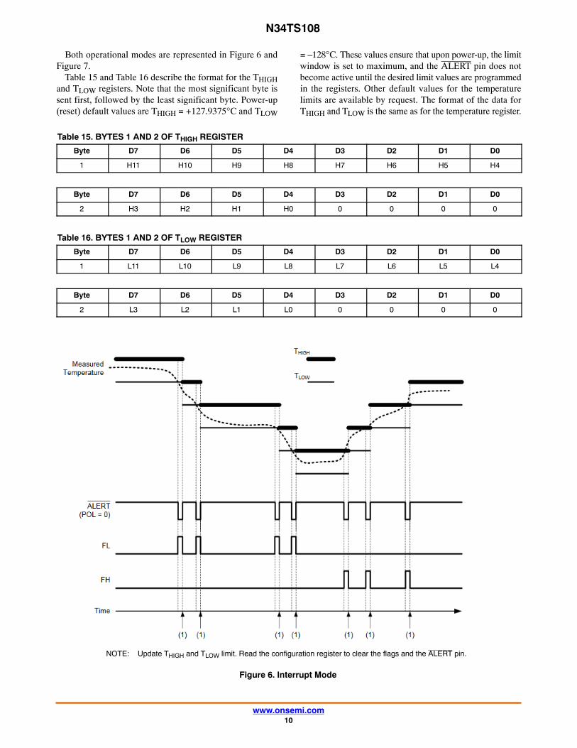
Both operational modes are represented in Figure 6 andFigure 7.
Table 15 and Table 16 describe the format for the THIGHand TLOW registers. Note that the most significant byte issent first, followed by the least significant byte. Power-up(reset) default values are THIGH = +127.9375°C and TLOW
= –128°C. These values ensure that upon power-up, the limitwindow is set to maximum, and the ALERT pin does notbecome active until the desired limit values are programmedin the registers. Other default values for the temperaturelimits are available by request. The format of the data forTHIGH and TLOW is the same as for the temperature register.
Table 15. BYTES 1 AND 2 OF THIGH REGISTER
Byte D7 D6 D5 D4 D3 D2 D1 D0
1 H11 H10 H9 H8 H7 H6 H5 H4
Byte D7 D6 D5 D4 D3 D2 D1 D0
2 H3 H2 H1 H0 0 0 0 0
Table 16. BYTES 1 AND 2 OF TLOW REGISTER
Byte D7 D6 D5 D4 D3 D2 D1 D0
1 L11 L10 L9 L8 L7 L6 L5 L4
Byte D7 D6 D5 D4 D3 D2 D1 D0
2 L3 L2 L1 L0 0 0 0 0
Figure 6. Interrupt Mode
NOTE: Update THIGH and TLOW limit. Read the configuration register to clear the flags and the ALERT pin.

N34TS108
www.onsemi.com11
Figure 7. Comparator Mode
SERIAL INTERFACEThe N34TS108 operates as a slave device only on the
two-wire bus and SMBus. Connections to the bus are madeusing the open-drain I/O lines, SDA and SCL. The SDA andSCL pins feature integrated spike-suppression filters andSchmitt triggers to minimize the effects of input spikes andbus noise. The N34TS108 supports the transmissionprotocol for both fast (1 kHz to 400 kHz) and high-speed(1 kHz to 3.4 MHz) modes. All data bytes are transmittedMSB first.
SERIAL BUS ADDRESSTo communicate with the N34TS108, the master must
first communicate with slave devices using a slave addressbyte. The slave address byte consists of seven address bits,and a direction bit indicating the intent of executing eithera read or write operation. The N34TS108 features an addresspin that allows up to three devices to be addressed on a singlebus. The N34TS108 latches the status of the address pin atthe start of a communication. Table 17 describes the pinlogic levels and the corresponding address values. Othervalues for the fixed address bits are available by request.
Table 17. ADDRESS PIN AND SLAVE ADDRESSES
Device Two-wire Address A0 Pin Connection
1001000 GND
1001001 VCC
1001010 SDA
BUS OVERVIEWThe device that initiates the transfer is called a master, and
the devices controlled by the master are slaves. The bus mustbe controlled by a master device that generates the serialclock (SCL), controls the bus access, and generates the startand stop conditions.
To address a specific device, initiate a start condition bypulling the data line (SDA) from a high to a low logic levelwhile SCL is high. All slaves on the bus shift in the slaveaddress byte; the last bit indicates whether a read or writeoperation follows. During the ninth clock pulse, the slavebeing addressed responds to the master by generating anacknowledge bit and pulling SDA low.
Data transfer is then initiated and sent over eight clockpulses followed by an acknowledge bit. During data transfer,SDA must remain stable while SCL is high because anychange in SDA while SCL is high is interpreted as a start orstop signal.
After all data have been transferred, the master generatesa stop condition indicated by pulling SDA from low to high,while SCL is high.
WRITING/READING OPERATIONAccessing a particular register on the N34TS108 is
accomplished by writing the appropriate value to the pointerregister. The value for the pointer register is the first bytetransferred after the slave address byte with the R/W bit low.Every write operation to the N34TS108 requires a value forthe pointer register.
When reading from the N34TS108, the last value storedin the pointer register by a write operation is used todetermine which register is read by a read operation. Tochange the register pointer for a read operation, a new valuemust be written to the pointer register. This action isaccomplished by issuing a slave address byte with the R/Wbit low, followed by the pointer register byte. No additional

N34TS108
www.onsemi.com12
data are required. The master can then generate a startcondition and send the slave address byte with the R/W bithigh to initiate the read command. If repeated reads from thesame register are desired, it is not necessary to continuallysend the pointer register bytes because the N34TS108 storesthe pointer register value until it is changed by the next writeoperation.
Note that register bytes are sent with the most significantbyte first, followed by the least significant byte.
SLAVE MODE OPERATIONSThe N34TS108 can operate as a slave receiver or slave
transmitter.
Slave Receiver Mode:The first byte transmitted by the master is the slave
address, with the R/W bit low. The N34TS108 thenacknowledges reception of a valid address. The next bytetransmitted by the master is the pointer register. TheN34TS108 then acknowledges reception of the pointerregister byte. The next byte or bytes are written to theregister addressed by the pointer register. The N34TS108acknowledges reception of each data byte. The master canterminate data transfer by generating a start or stopcondition.
Slave Transmitter Mode:The first byte transmitted by the master is the slave
address, with the R/W bit high. The slave acknowledgesreception of a valid slave address. The next byte istransmitted by the slave and is the most significant byte ofthe register indicated by the pointer register. The masteracknowledges reception of the data byte. The next bytetransmitted by the slave is the least significant byte. Themaster acknowledges reception of the data byte. The mastercan terminate data transfer by generating a not-acknowledgebit on reception of any data byte, or by generating a start orstop condition.
SMBus ALERT FUNCTIONThe N34TS108 supports the SMBus alert function. When
the N34TS108 operates in interrupt mode (TM = ‘1’), theALERT pin may be connected as an SMBus alert signal.When a master senses that an alert condition is present on theALERT line, the master sends an SMBus alert command(00011001) to the bus. If the ALERT pin is active, the deviceacknowledges the SMBus alert command and responds byreturning its slave address on the SDA line. The eighth bit
(LSB) of the slave address byte indicates whether the alertcondition is caused by the temperature exceeding THIGH orfalling below TLOW. The LSB is high if the temperature isgreater than THIGH, or low if the temperature is less thanTLOW.
If multiple devices on the bus respond to the SMBus alertcommand, arbitration during the slave address portion of theSMBus alert command determines which device clears itsalert status first. If the N34TS108 wins the arbitration, itsALERT pin becomes inactive at the completion of theSMBus alert command. If the N34TS108 loses thearbitration, its ALERT pin remains active.
GENERAL CALLThe N34TS108 responds to a two-wire general call
address (0000000) if the eighth bit is ‘0’. The deviceacknowledges the general call address and responds tocommands in the second byte. If the second byte is
00000100, the N34TS108 latches the status of the addresspin, but does not reset. If the second byte is 00000110, theN34TS108 internal registers are reset to power-up values.The N34TS108 does not support the general address acquirecommand.
HIGH-SPEED (Hs) MODEIn order for the two-wire bus to operate at frequencies
above 400 kHz, the master device must issue an SMBusHs-mode master code (00001xxx) as the first byte aftera start condition to switch the bus to high-speed operation.The N34TS108 does not acknowledge this byte, but doesswitch its input filters on SDA and SCL and its output filterson SDA to operate in Hs-mode, allowing transfers at up to3.4 MHz. After the Hs-mode master code has been issued,the master transmits a two-wire slave address to initiatea data-transfer operation. The bus continues to operate inHs-mode until a stop condition occurs on the bus. Uponreceiving the stop condition, the N34TS108 switches theinput and output filters back to fast-mode operation.
TIMEOUT FUNCTIONThe N34TS108 resets the serial interface if SCL or SDA
are held low for 30 ms (typ) between a start and stopcondition. If the N34TS108 is pulled low, it releases the busand then waits for a start condition. To avoid activating thetimeout function, it is necessary to maintaina communication speed of at least 1 kHz for the SCLoperating frequency.
N34TS108
www.onsemi.com13
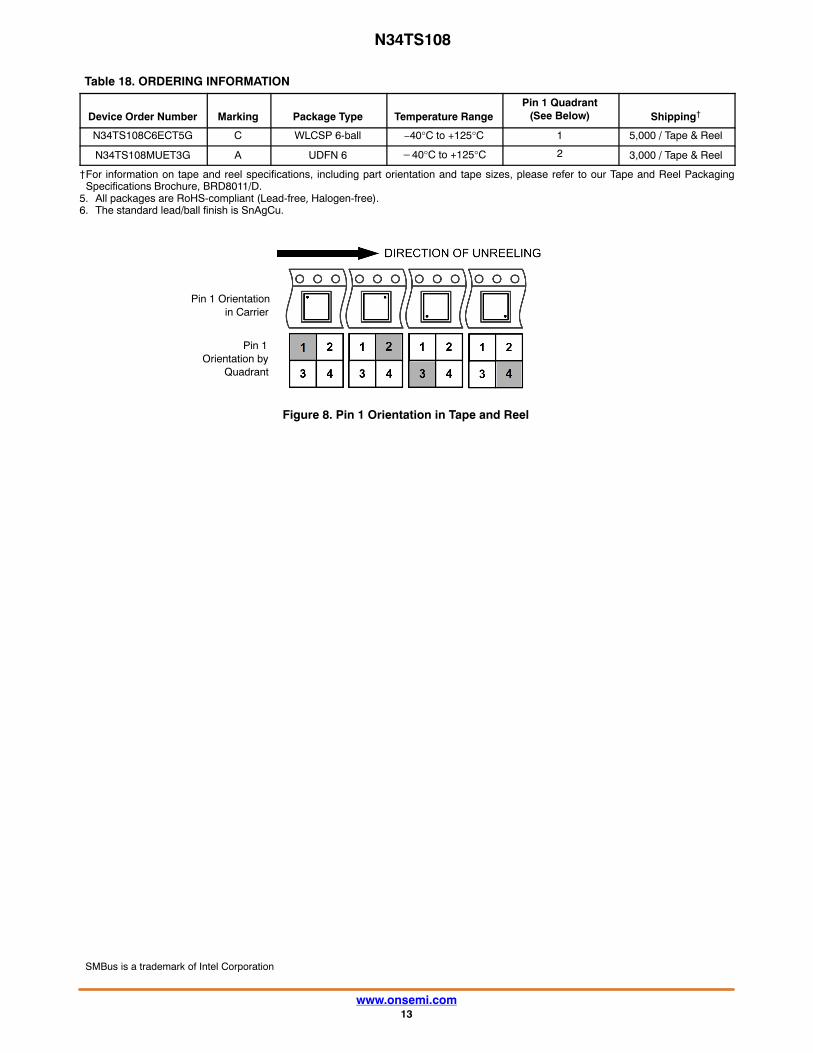
Table 18. ORDERING INFORMATION
Device Order Number Marking Package Type Temperature RangePin 1 Quadrant
(See Below) Shipping†
N34TS108C6ECT5G C WLCSP 6-ball −40°C to +125°C 1 5,000 / Tape & Reel
N34TS108MUET3G A UDFN 6 �40°C to +125°C 2 3,000 / Tape & Reel
†For information on tape and reel specifications, including part orientation and tape sizes, please refer to our Tape and Reel PackagingSpecifications Brochure, BRD8011/D.
5. All packages are RoHS-compliant (Lead-free, Halogen-free).6. The standard lead/ball finish is SnAgCu.
Figure 8. Pin 1 Orientation in Tape and Reel
Pin 1 Orientationin Carrier
Pin 1Orientation by
Quadrant
SMBus is a trademark of Intel Corporation
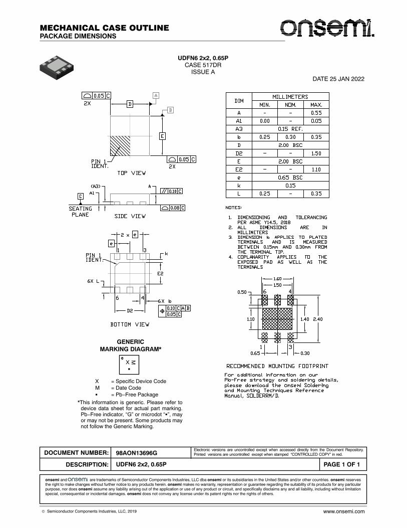
UDFN6 2x2, 0.65PCASE 517DR
ISSUE ADATE 25 JAN 2022
X = Specific Device CodeM = Date Code� = Pb−Free Package
*This information is generic. Please refer todevice data sheet for actual part marking.Pb−Free indicator, “G” or microdot “�”, mayor may not be present. Some products maynot follow the Generic Marking.
GENERICMARKING DIAGRAM*
X �
M
MECHANICAL CASE OUTLINE
PACKAGE DIMENSIONS
98AON13696GDOCUMENT NUMBER:
DESCRIPTION:
Electronic versions are uncontrolled except when accessed directly from the Document Repository.Printed versions are uncontrolled except when stamped “CONTROLLED COPY” in red.
PAGE 1 OF 1UDFN6 2x2, 0.65P
onsemi and are trademarks of Semiconductor Components Industries, LLC dba onsemi or its subsidiaries in the United States and/or other countries. onsemi reservesthe right to make changes without further notice to any products herein. onsemi makes no warranty, representation or guarantee regarding the suitability of its products for any particularpurpose, nor does onsemi assume any liability arising out of the application or use of any product or circuit, and specifically disclaims any and all liability, including without limitationspecial, consequential or incidental damages. onsemi does not convey any license under its patent rights nor the rights of others.
© Semiconductor Components Industries, LLC, 2019 www.onsemi.com
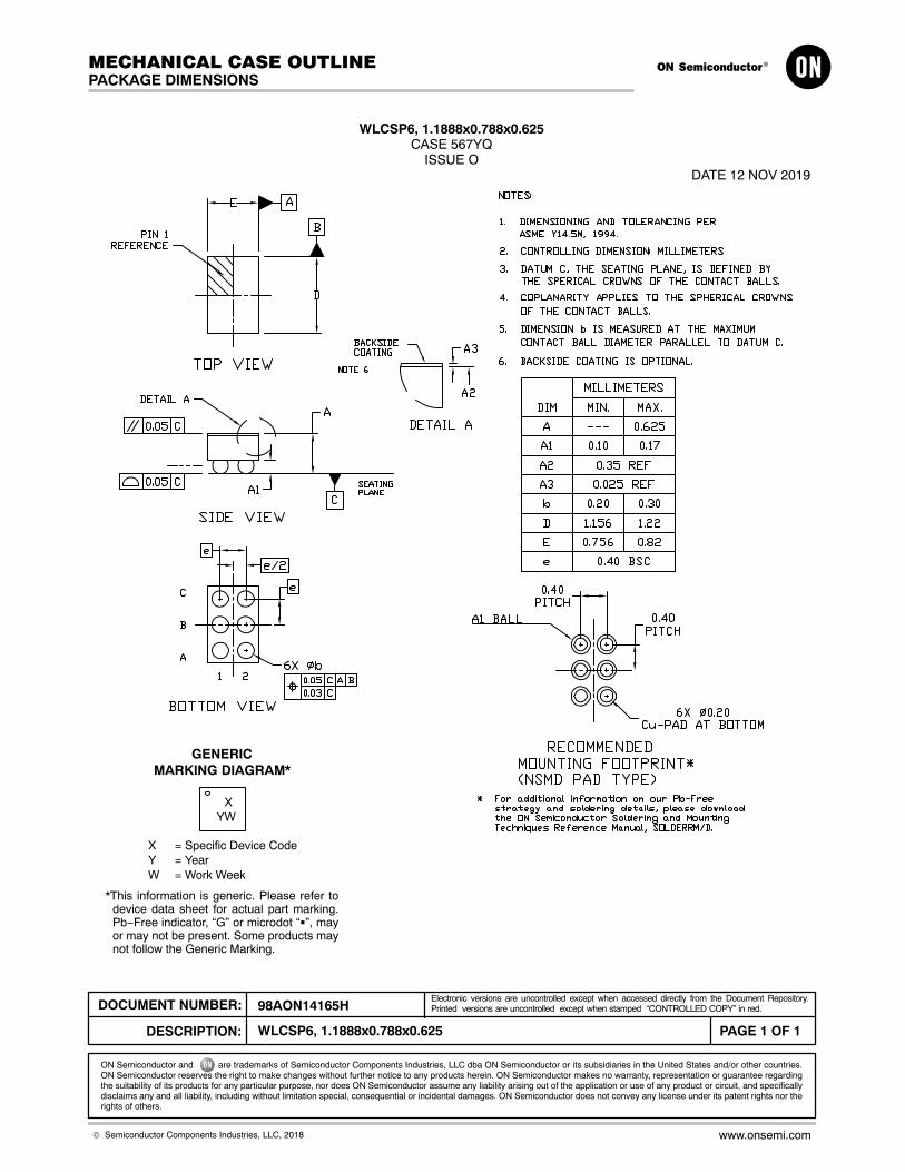
WLCSP6, 1.1888x0.788x0.625CASE 567YQ
ISSUE ODATE 12 NOV 2019
GENERICMARKING DIAGRAM*
*This information is generic. Please refer todevice data sheet for actual part marking.Pb−Free indicator, “G” or microdot “�”, mayor may not be present. Some products maynot follow the Generic Marking.
X = Specific Device CodeY = YearW = Work Week
X YW
MECHANICAL CASE OUTLINE
PACKAGE DIMENSIONS
ON Semiconductor and are trademarks of Semiconductor Components Industries, LLC dba ON Semiconductor or its subsidiaries in the United States and/or other countries.ON Semiconductor reserves the right to make changes without further notice to any products herein. ON Semiconductor makes no warranty, representation or guarantee regardingthe suitability of its products for any particular purpose, nor does ON Semiconductor assume any liability arising out of the application or use of any product or circuit, and specificallydisclaims any and all liability, including without limitation special, consequential or incidental damages. ON Semiconductor does not convey any license under its patent rights nor therights of others.
98AON14165HDOCUMENT NUMBER:
DESCRIPTION:
Electronic versions are uncontrolled except when accessed directly from the Document Repository.Printed versions are uncontrolled except when stamped “CONTROLLED COPY” in red.
PAGE 1 OF 1WLCSP6, 1.1888x0.788x0.625
© Semiconductor Components Industries, LLC, 2018 www.onsemi.com

onsemi, , and other names, marks, and brands are registered and/or common law trademarks of Semiconductor Components Industries, LLC dba “onsemi” or its affiliatesand/or subsidiaries in the United States and/or other countries. onsemi owns the rights to a number of patents, trademarks, copyrights, trade secrets, and other intellectual property.A listing of onsemi’s product/patent coverage may be accessed at www.onsemi.com/site/pdf/Patent−Marking.pdf. onsemi reserves the right to make changes at any time to anyproducts or information herein, without notice. The information herein is provided “as−is” and onsemi makes no warranty, representation or guarantee regarding the accuracy of theinformation, product features, availability, functionality, or suitability of its products for any particular purpose, nor does onsemi assume any liability arising out of the application or useof any product or circuit, and specifically disclaims any and all liability, including without limitation special, consequential or incidental damages. Buyer is responsible for its productsand applications using onsemi products, including compliance with all laws, regulations and safety requirements or standards, regardless of any support or applications informationprovided by onsemi. “Typical” parameters which may be provided in onsemi data sheets and/or specifications can and do vary in different applications and actual performance mayvary over time. All operating parameters, including “Typicals” must be validated for each customer application by customer’s technical experts. onsemi does not convey any licenseunder any of its intellectual property rights nor the rights of others. onsemi products are not designed, intended, or authorized for use as a critical component in life support systemsor any FDA Class 3 medical devices or medical devices with a same or similar classification in a foreign jurisdiction or any devices intended for implantation in the human body. ShouldBuyer purchase or use onsemi products for any such unintended or unauthorized application, Buyer shall indemnify and hold onsemi and its officers, employees, subsidiaries, affiliates,and distributors harmless against all claims, costs, damages, and expenses, and reasonable attorney fees arising out of, directly or indirectly, any claim of personal injury or deathassociated with such unintended or unauthorized use, even if such claim alleges that onsemi was negligent regarding the design or manufacture of the part. onsemi is an EqualOpportunity/Affirmative Action Employer. This literature is subject to all applicable copyright laws and is not for resale in any manner.
PUBLICATION ORDERING INFORMATIONTECHNICAL SUPPORTNorth American Technical Support:Voice Mail: 1 800−282−9855 Toll Free USA/CanadaPhone: 011 421 33 790 2910
LITERATURE FULFILLMENT:Email Requests to: [email protected]
onsemi Website: www.onsemi.com
Europe, Middle East and Africa Technical Support:Phone: 00421 33 790 2910For additional information, please contact your local Sales Representative
◊


