
March 18, 2009
© SOFTHARD Technology Ltd
Lesna 52, 900 33 Marianka
Slovak Republic
MR11002 Image Acquisition Timings using Hardware Trigger
Page 2
1 Table of Contents
1 Table of Contents ......................................................................... 2
2 Revision History ........................................................................... 3
3 Disclaimers ................................................................................... 4
4 Privacy Information ...................................................................... 4
5 Document Scope and Purpose ...................................................... 4
6 Set up ........................................................................................... 4
7 Conclusion .................................................................................... 9

MR11002 Image Acquisition Timings using Hardware Trigger
Page 3
2 Revision History
Revision Date Who What
0.10 17.03.2009 MK First version of application note.

MR11002 Image Acquisition Timings using Hardware Trigger
Page 4
3 Disclaimers
The information contained in this document is the proprietary and exclusive
property of SOFTHARD Technology Ltd except as otherwise indicated. No part of this document, in whole or in part, may be reproduced, stored,
transmitted, or used for design purposes without the prior permission of SOFTHARD Technology Ltd.
Information provided in this document is subject to change without notice.
4 Privacy Information
This document contains information of a sensitive nature. This information
should not be given to persons other than those who are involved in the
MR11002 project or who will become involved during the lifecycle.
5 Document Scope and Purpose
This document describes image acquisition timings of the MR11002 camera when using hardware trigger.
6 Set up
The measurement setup consists of MR11002 camera, FPGA development board, high brightness LED and HP Infinium Digital Oscilloscope. The FPGA generates hardware trigger signal for MR11002 camera upon pressing a
button. Also it generates a 10µs LED pulse with a certain offset with respect to the trigger pulse. The trigger signal triggers MR11002 camera to capture
an image, which is then analyzed, namely whether or not the LED pulse is captured on the image.
On the following screenshots from the oscilloscope the LED signal (active low)
is shown in yellow color and the MR11002 trigger signal (rising edge) is green.

MR11002 Image Acquisition Timings using Hardware Trigger
Page 5
The initial LED pulse offset with respect to the trigger signal is 10µs. That means that LED is turned off 10µs before the trigger signal for MR11002 is
issued. In this situation we don’t expect to see light from the LED on the images and it is purely for completeness of the experiment.
After issuing several such pulses and analyzing acquired images, the LED pulse is shifted to the right with respect to the trigger pulse in 2µs discrete
steps and more images are taken.
By shifting LED signal to the right until it start appearing on the acquired images we can measure the offset between the issued trigger pulse and the
start of image acquisition.
MR11002 Image Acquisition Timings using Hardware Trigger
Page 6
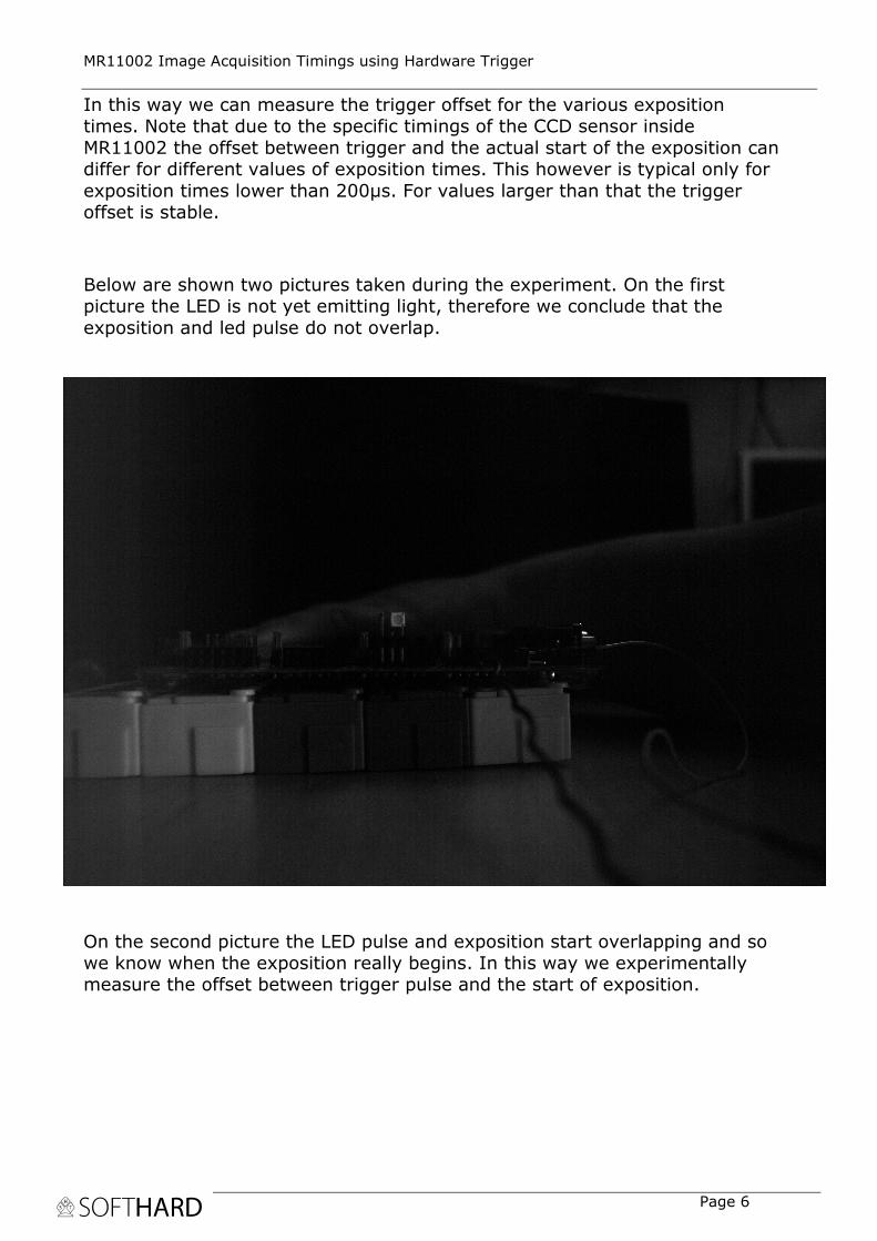
In this way we can measure the trigger offset for the various exposition times. Note that due to the specific timings of the CCD sensor inside
MR11002 the offset between trigger and the actual start of the exposition can differ for different values of exposition times. This however is typical only for
exposition times lower than 200µs. For values larger than that the trigger offset is stable.
Below are shown two pictures taken during the experiment. On the first picture the LED is not yet emitting light, therefore we conclude that the
exposition and led pulse do not overlap.
On the second picture the LED pulse and exposition start overlapping and so we know when the exposition really begins. In this way we experimentally measure the offset between trigger pulse and the start of exposition.

MR11002 Image Acquisition Timings using Hardware Trigger
Page 7
7 Results
The following offsets from trigger impulse to start of exposition have been measured for the different values of exposition time. (Note that offset value change was observed to change in steps and not linearly)
Exposition Offset Total Time
1000 2000 2000
500 1000 1000
430 860 860
429 858 858
428 856 856
419 838 838
418 836 836
409 818 818
408 816 816
219 438 438
218 436 436
43 86 86
42 84 84
23 46 46
22 44 44
MR11002 Image Acquisition Timings using Hardware Trigger
Page 8
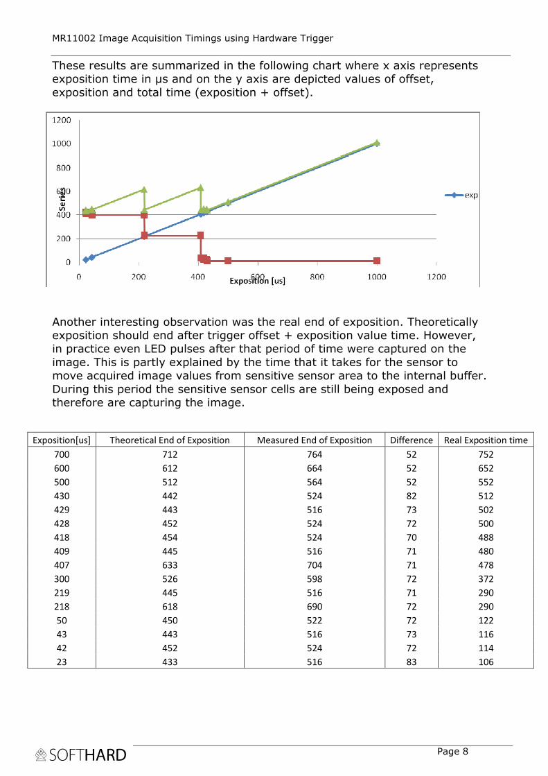
These results are summarized in the following chart where x axis represents exposition time in µs and on the y axis are depicted values of offset,
exposition and total time (exposition + offset).
Another interesting observation was the real end of exposition. Theoretically exposition should end after trigger offset + exposition value time. However, in practice even LED pulses after that period of time were captured on the
image. This is partly explained by the time that it takes for the sensor to move acquired image values from sensitive sensor area to the internal buffer.
During this period the sensitive sensor cells are still being exposed and therefore are capturing the image.
Exposition[us] Theoretical End of Exposition Measured End of Exposition Difference Real Exposition time
700 712 764 52 752
600 612 664 52 652
500 512 564 52 552
430 442 524 82 512
429 443 516 73 502
428 452 524 72 500
418 454 524 70 488
409 445 516 71 480
407 633 704 71 478
300 526 598 72 372
219 445 516 71 290
218 618 690 72 290
50 450 522 72 122
43 443 516 73 116
42 452 524 72 114
23 433 516 83 106

MR11002 Image Acquisition Timings using Hardware Trigger
Page 9
8 Conclusion
An experimental measurement of hardware trigger timings for MR11002 was performed. Offset time between issuing a trigger and the actual start of acquisition was measured and depicted in a chart. It can be concluded that for exposition times greater than 430µs the offset is constant and equal to 12µs, so the image acquisition start precisely 12 µs after a trigger is received by MR11002 camera. For exposition values lower than 430µs the offset increases in steps and therefore the exposition starts with a delay. Therefore for applications where it is important to know the precise time when exposition was started it is recommended to use exposition times greater than 430 µs, which is sufficient for most of the typical applications. For applications where it is absolutely necessary to use exposition times lower than 430 µs it is important to bear in mind the increasing time offset between trigger and the start of exposition and include that in the subsequent calculations and results. Another aspect covered in the performed measurements is real exposition duration. Due to the fact that sensor continues image acquisition during the data transfer from the sensitive part to the internal buffer, the real exposition time is somewhat prolonged. For applications that are very sensitive to this characteristics, these results should also be considered.


