© 2010 Freescale Semiconductor, Inc. All rights reserved.
Freescale SemiconductorTechnical Data
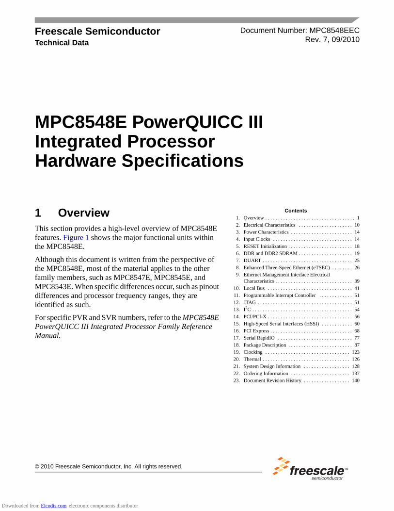
1 OverviewThis section provides a high-level overview of MPC8548E features. Figure 1 shows the major functional units within the MPC8548E.
Although this document is written from the perspective of the MPC8548E, most of the material applies to the other family members, such as MPC8547E, MPC8545E, and MPC8543E. When specific differences occur, such as pinout differences and processor frequency ranges, they are identified as such.
For specific PVR and SVR numbers, refer to the MPC8548E PowerQUICC III Integrated Processor Family Reference Manual.
Contents1. Overview . . . . . . . . . . . . . . . . . . . . . . . . . . . . . . . . . . . 12. Electrical Characteristics . . . . . . . . . . . . . . . . . . . . . 103. Power Characteristics . . . . . . . . . . . . . . . . . . . . . . . . 144. Input Clocks . . . . . . . . . . . . . . . . . . . . . . . . . . . . . . . 145. RESET Initialization . . . . . . . . . . . . . . . . . . . . . . . . . 186. DDR and DDR2 SDRAM . . . . . . . . . . . . . . . . . . . . . 197. DUART . . . . . . . . . . . . . . . . . . . . . . . . . . . . . . . . . . . 258. Enhanced Three-Speed Ethernet (eTSEC) . . . . . . . . 269. Ethernet Management Interface Electrical
Characteristics . . . . . . . . . . . . . . . . . . . . . . . . . . . . . . 3910. Local Bus . . . . . . . . . . . . . . . . . . . . . . . . . . . . . . . . . 4111. Programmable Interrupt Controller . . . . . . . . . . . . . 5112. JTAG . . . . . . . . . . . . . . . . . . . . . . . . . . . . . . . . . . . . . 5113. I2C . . . . . . . . . . . . . . . . . . . . . . . . . . . . . . . . . . . . . . . 5414. PCI/PCI-X . . . . . . . . . . . . . . . . . . . . . . . . . . . . . . . . . 5615. High-Speed Serial Interfaces (HSSI) . . . . . . . . . . . . 6016. PCI Express . . . . . . . . . . . . . . . . . . . . . . . . . . . . . . . . 6817. Serial RapidIO . . . . . . . . . . . . . . . . . . . . . . . . . . . . . 7718. Package Description . . . . . . . . . . . . . . . . . . . . . . . . . 8719. Clocking . . . . . . . . . . . . . . . . . . . . . . . . . . . . . . . . . 12320. Thermal . . . . . . . . . . . . . . . . . . . . . . . . . . . . . . . . . . 12621. System Design Information . . . . . . . . . . . . . . . . . . 12822. Ordering Information . . . . . . . . . . . . . . . . . . . . . . . 13723. Document Revision History . . . . . . . . . . . . . . . . . . 140
MPC8548E PowerQUICC IIIIntegrated ProcessorHardware Specifications
Document Number: MPC8548EECRev. 7, 09/2010
Downloaded from Elcodis.com electronic components distributor

MPC8548E PowerQUICC III Integrated Processor Hardware Specifications, Rev. 7
2 Freescale Semiconductor
Overview
Figure 1. MPC8548E Block Diagram
1.1 Key FeaturesThe following list provides an overview of the MPC8548E feature set:
• High-performance 32-bit core built on Power Architecture® technology.— 32-Kbyte L1 instruction cache and 32-Kbyte L1 data cache with parity protection. Caches can
be locked entirely or on a per-line basis, with separate locking for instructions and data.— Signal-processing engine (SPE) APU (auxiliary processing unit). Provides an extensive
instruction set for vector (64-bit) integer and fractional operations. These instructions use both the upper and lower words of the 64-bit GPRs as they are defined by the SPE APU.
— Double-precision floating-point APU. Provides an instruction set for double-precision (64-bit) floating-point instructions that use the 64-bit GPRs.
— 36-bit real addressing— Embedded vector and scalar single-precision floating-point APUs. Provide an instruction set
for single-precision (32-bit) floating-point instructions.— Memory management unit (MMU). Especially designed for embedded applications. Supports
4-Kbyte to 4-Gbyte page sizes.— Enhanced hardware and software debug support
Core Complex
x8 PCI Express4x RapidIO
66 MHzPCI 32-bit
10/100/1Gb
MII, GMII, TBI,RTBI, RGMII,
Serial
IRQs
SDRAMDDR
FlashSDRAM
GPIO
Bus
I2CI2C
Controller
eTSEC
32-bit PCI Bus Interface(If 64-bit not used)
e500Coherency
Module
DDR/DDR2/Memory Controller
Local Bus Controller
Programmable Interrupt Controller (PIC)
DUART
e500 Core
512-Kbyte L2 Cache/
SRAM
32-bit PCI/64-bit PCI/PCI-X
Bus Interface
32-Kbyte L1 Instruction
Cache
32-Kbyte L1 Data Cache
OceaN Switch Fabric
Serial RapidIOor
PCI Express
4-Channel DMA Controller
133 MHzPCI/PCI-X
I2CI2C
Controller
RMII
10/100/1Gb
MII, GMII, TBI,RTBI, RGMII,
eTSEC
RMII
10/100/1Gb
MII, GMII, TBI,RTBI, RGMII,
eTSEC
RMII
10/100/1Gb
RTBI, RGMII, eTSEC
Security Engine
XOREngine
RMII
Downloaded from Elcodis.com electronic components distributor

MPC8548E PowerQUICC III Integrated Processor Hardware Specifications, Rev. 7
Freescale Semiconductor 3
Overview
— Performance monitor facility that is similar to, but separate from, the MPC8548E performance monitor
The e500 defines features that are not implemented on this device. It also generally defines some features that this device implements more specifically. An understanding of these differences can be critical to ensure proper operations.
• 512-Kbyte L2 cache/SRAM— Flexible configuration.— Full ECC support on 64-bit boundary in both cache and SRAM modes— Cache mode supports instruction caching, data caching, or both.— External masters can force data to be allocated into the cache through programmed memory
ranges or special transaction types (stashing). — 1, 2, or 4 ways can be configured for stashing only.— Eight-way set-associative cache organization (32-byte cache lines)— Supports locking entire cache or selected lines. Individual line locks are set and cleared through
Book E instructions or by externally mastered transactions.— Global locking and Flash clearing done through writes to L2 configuration registers— Instruction and data locks can be Flash cleared separately.— SRAM features include the following:
– I/O devices access SRAM regions by marking transactions as snoopable (global).– Regions can reside at any aligned location in the memory map.– Byte-accessible ECC is protected using read-modify-write transaction accesses for
smaller-than-cache-line accesses.• Address translation and mapping unit (ATMU)
— Eight local access windows define mapping within local 36-bit address space.— Inbound and outbound ATMUs map to larger external address spaces.
– Three inbound windows plus a configuration window on PCI/PCI-X and PCI Express– Four inbound windows plus a default window on RapidIO™ – Four outbound windows plus default translation for PCI/PCI-X and PCI Express– Eight outbound windows plus default translation for RapidIO with segmentation and
sub-segmentation support• DDR/DDR2 memory controller
— Programmable timing supporting DDR and DDR2 SDRAM— 64-bit data interface— Four banks of memory supported, each up to 4 Gbytes, to a maximum of 16 Gbytes— DRAM chip configurations from 64 Mbits to 4 Gbits with ×8/×16 data ports— Full ECC support— Page mode support
– Up to 16 simultaneous open pages for DDR
Downloaded from Elcodis.com electronic components distributor

MPC8548E PowerQUICC III Integrated Processor Hardware Specifications, Rev. 7
4 Freescale Semiconductor
Overview
– Up to 32 simultaneous open pages for DDR2— Contiguous or discontiguous memory mapping— Read-modify-write support for RapidIO atomic increment, decrement, set, and clear
transactions— Sleep mode support for self-refresh SDRAM— On-die termination support when using DDR2— Supports auto refreshing— On-the-fly power management using CKE signal— Registered DIMM support— Fast memory access via JTAG port— 2.5-V SSTL_2 compatible I/O (1.8-V SSTL_1.8 for DDR2)— Support for battery-backed main memory
• Programmable interrupt controller (PIC)— Programming model is compliant with the OpenPIC architecture.— Supports 16 programmable interrupt and processor task priority levels— Supports 12 discrete external interrupts— Supports 4 message interrupts with 32-bit messages— Supports connection of an external interrupt controller such as the 8259 programmable
interrupt controller— Four global high-resolution timers/counters that can generate interrupts— Supports a variety of other internal interrupt sources— Supports fully nested interrupt delivery— Interrupts can be routed to external pin for external processing.— Interrupts can be routed to the e500 core’s standard or critical interrupt inputs.— Interrupt summary registers allow fast identification of interrupt source.
• Integrated security engine (SEC) optimized to process all the algorithms associated with IPSec, IKE, WTLS/WAP, SSL/TLS, and 3GPP— Four crypto-channels, each supporting multi-command descriptor chains
– Dynamic assignment of crypto-execution units via an integrated controller– Buffer size of 256 bytes for each execution unit, with flow control for large data sizes
— PKEU—public key execution unit– RSA and Diffie-Hellman; programmable field size up to 2048 bits– Elliptic curve cryptography with F2m and F(p) modes and programmable field size up to
511 bits— DEU—Data Encryption Standard execution unit
– DES, 3DES – Two key (K1, K2) or three key (K1, K2, K3)– ECB and CBC modes for both DES and 3DES
Downloaded from Elcodis.com electronic components distributor

MPC8548E PowerQUICC III Integrated Processor Hardware Specifications, Rev. 7
Freescale Semiconductor 5
Overview
— AESU—Advanced Encryption Standard unit– Implements the Rijndael symmetric key cipher– ECB, CBC, CTR, and CCM modes– 128-, 192-, and 256-bit key lengths
— AFEU—ARC four execution unit– Implements a stream cipher compatible with the RC4 algorithm – 40- to 128-bit programmable key
— MDEU—message digest execution unit– SHA with 160- or 256-bit message digest – MD5 with 128-bit message digest– HMAC with either algorithm
— KEU—Kasumi execution unit – Implements F8 algorithm for encryption and F9 algorithm for integrity checking– Also supports A5/3 and GEA-3 algorithms
— RNG—random number generator— XOR engine for parity checking in RAID storage applications
• Dual I2C controllers— Two-wire interface— Multiple master support— Master or slave I2C mode support— On-chip digital filtering rejects spikes on the bus
• Boot sequencer— Optionally loads configuration data from serial ROM at reset via the I2C interface— Can be used to initialize configuration registers and/or memory— Supports extended I2C addressing mode— Data integrity checked with preamble signature and CRC
• DUART— Two 4-wire interfaces (SIN, SOUT, RTS, CTS)— Programming model compatible with the original 16450 UART and the PC16550D
• Local bus controller (LBC)— Multiplexed 32-bit address and data bus operating at up to 133 MHz— Eight chip selects support eight external slaves— Up to eight-beat burst transfers— The 32-, 16-, and 8-bit port sizes are controlled by an on-chip memory controller.— Three protocol engines available on a per chip select basis:
– General-purpose chip select machine (GPCM)– Three user programmable machines (UPMs)
Downloaded from Elcodis.com electronic components distributor

MPC8548E PowerQUICC III Integrated Processor Hardware Specifications, Rev. 7
6 Freescale Semiconductor
Overview
– Dedicated single data rate SDRAM controller— Parity support— Default boot ROM chip select with configurable bus width (8, 16, or 32 bits)
• Four enhanced three-speed Ethernet controllers (eTSECs)— Three-speed support (10/100/1000 Mbps)— Four controllers designed to comply with IEEE Stds. 802.3™, 802.3u™, 802.3x™, 802.3z™,
802.3ac™, and 802.3ab™— Support for various Ethernet physical interfaces:
– 1000 Mbps full-duplex IEEE 802.3 GMII, IEEE 802.3z TBI, RTBI, and RGMII– 10/100 Mbps full and half-duplex IEEE 802.3 MII, IEEE 802.3 RGMII, and RMII
— Flexible configuration for multiple PHY interface configurations. See Section 8.1, “Enhanced Three-Speed Ethernet Controller (eTSEC) (10/100/1Gb Mbps)—GMII/MII/TBI/RGMII/RTBI/RMII Electrical Characteristics,” for more information.
— TCP/IP acceleration and QoS features available– IP v4 and IP v6 header recognition on receive– IP v4 header checksum verification and generation– TCP and UDP checksum verification and generation– Per-packet configurable acceleration– Recognition of VLAN, stacked (queue in queue) VLAN, IEEE Std 802.2™, PPPoE session,
MPLS stacks, and ESP/AH IP-security headers– Supported in all FIFO modes
— Quality of service support:– Transmission from up to eight physical queues– Reception to up to eight physical queues
— Full- and half-duplex Ethernet support (1000 Mbps supports only full duplex):– IEEE 802.3 full-duplex flow control (automatic PAUSE frame generation or
software-programmed PAUSE frame generation and recognition)— Programmable maximum frame length supports jumbo frames (up to 9.6 Kbytes) and
IEEE Std. 802.1™ virtual local area network (VLAN) tags and priority— VLAN insertion and deletion
– Per-frame VLAN control word or default VLAN for each eTSEC– Extracted VLAN control word passed to software separately
— Retransmission following a collision— CRC generation and verification of inbound/outbound frames— Programmable Ethernet preamble insertion and extraction of up to 7 bytes— MAC address recognition:
– Exact match on primary and virtual 48-bit unicast addresses
Downloaded from Elcodis.com electronic components distributor

MPC8548E PowerQUICC III Integrated Processor Hardware Specifications, Rev. 7
Freescale Semiconductor 7
Overview
– VRRP and HSRP support for seamless router fail-over– Up to 16 exact-match MAC addresses supported– Broadcast address (accept/reject)– Hash table match on up to 512 multicast addresses– Promiscuous mode
— Buffer descriptors backward compatible with MPC8260 and MPC860T 10/100 Ethernet programming models
— RMON statistics support— 10-Kbyte internal transmit and 2-Kbyte receive FIFOs— MII management interface for control and status— Ability to force allocation of header information and buffer descriptors into L2 cache
• OCeaN switch fabric— Full crossbar packet switch— Reorders packets from a source based on priorities— Reorders packets to bypass blocked packets— Implements starvation avoidance algorithms— Supports packets with payloads of up to 256 bytes
• Integrated DMA controller— Four-channel controller— All channels accessible by both the local and remote masters— Extended DMA functions (advanced chaining and striding capability)— Support for scatter and gather transfers— Misaligned transfer capability— Interrupt on completed segment, link, list, and error— Supports transfers to or from any local memory or I/O port— Selectable hardware-enforced coherency (snoop/no snoop)— Ability to start and flow control each DMA channel from external 3-pin interface— Ability to launch DMA from single write transaction
• Two PCI/PCI-X controllers— PCI 2.2 and PCI-X 1.0 compatible — One 32-/64-bit PCI/PCI-X port with support for speeds of up to 133 MHz (maximum PCI-X
frequency in synchronous mode is 110 MHz)— One 32-bit PCI port with support for speeds from 16 to 66 MHz (available when the other port
is in 32-bit mode)— Host and agent mode support— 64-bit dual address cycle (DAC) support— PCI-X supports multiple split transactions— Supports PCI-to-memory and memory-to-PCI streaming
Downloaded from Elcodis.com electronic components distributor

MPC8548E PowerQUICC III Integrated Processor Hardware Specifications, Rev. 7
8 Freescale Semiconductor
Overview
— Memory prefetching of PCI read accesses— Supports posting of processor-to-PCI and PCI-to-memory writes— PCI 3.3-V compatible— Selectable hardware-enforced coherency
• Serial RapidIO™ interface unit— Supports RapidIO™ Interconnect Specification, Revision 1.2— Both 1× and 4× LP-serial link interfaces — Long- and short-haul electricals with selectable pre-compensation— Transmission rates of 1.25, 2.5, and 3.125 Gbaud (data rates of 1.0, 2.0, and 2.5 Gbps) per lane— Auto detection of 1×- and 4×-mode operation during port initialization— Link initialization and synchronization— Large and small size transport information field support selectable at initialization time— 34-bit addressing— Up to 256 bytes data payload— All transaction flows and priorities— Atomic set/clr/inc/dec for read-modify-write operations— Generation of IO_READ_HOME and FLUSH with data for accessing cache-coherent data at
a remote memory system— Receiver-controlled flow control— Error detection, recovery, and time-out for packets and control symbols as required by the
RapidIO specification— Register and register bit extensions as described in part VIII (Error Management) of the
RapidIO specification— Hardware recovery only— Register support is not required for software-mediated error recovery.— Accept-all mode of operation for fail-over support— Support for RapidIO error injection— Internal LP-serial and application interface-level loopback modes— Memory and PHY BIST for at-speed production test
• RapidIO-compatible message unit— 4 Kbytes of payload per message — Up to sixteen 256-byte segments per message— Two inbound data message structures within the inbox— Capable of receiving three letters at any mailbox— Two outbound data message structures within the outbox— Capable of sending three letters simultaneously— Single segment multicast to up to 32 devIDs— Chaining and direct modes in the outbox
Downloaded from Elcodis.com electronic components distributor

MPC8548E PowerQUICC III Integrated Processor Hardware Specifications, Rev. 7
Freescale Semiconductor 9
Overview
— Single inbound doorbell message structure— Facility to accept port-write messages
• PCI Express interface— PCI Express 1.0a compatible— Supports ×8, ×4, ×2, and ×1 link widths— Auto-detection of number of connected lanes— Selectable operation as root complex or endpoint— Both 32- and 64-bit addressing— 256-byte maximum payload size— Virtual channel 0 only— Traffic class 0 only— Full 64-bit decode with 32-bit wide windows
• Pin multiplexing for the high-speed I/O interfaces supports one of the following configurations:— ×8 PCI Express— ×4 PCI Express and 4× serial RapidIO
• Power management— Supports power saving modes: doze, nap, and sleep— Employs dynamic power management, which automatically minimizes power consumption of
blocks when they are idle• System performance monitor
— Supports eight 32-bit counters that count the occurrence of selected events— Ability to count up to 512 counter-specific events— Supports 64 reference events that can be counted on any of the eight counters— Supports duration and quantity threshold counting — Burstiness feature that permits counting of burst events with a programmable time between
bursts— Triggering and chaining capability— Ability to generate an interrupt on overflow
• System access port— Uses JTAG interface and a TAP controller to access entire system memory map— Supports 32-bit accesses to configuration registers— Supports cache-line burst accesses to main memory— Supports large block (4-Kbyte) uploads and downloads— Supports continuous bit streaming of entire block for fast upload and download
• JTAG boundary scan, designed to comply with IEEE Std. 1149.1™
Downloaded from Elcodis.com electronic components distributor

MPC8548E PowerQUICC III Integrated Processor Hardware Specifications, Rev. 7
10 Freescale Semiconductor
Electrical Characteristics
2 Electrical CharacteristicsThis section provides the AC and DC electrical specifications and thermal characteristics for the MPC8548E. This device is currently targeted to these specifications. Some of these specifications are independent of the I/O cell, but are included for a more complete reference. These are not purely I/O buffer design specifications.
2.1 Overall DC Electrical CharacteristicsThis section covers the ratings, conditions, and other characteristics.
2.1.1 Absolute Maximum RatingsTable 1 provides the absolute maximum ratings.
Table 1. Absolute Maximum Ratings 1
Characteristic Symbol Max Value Unit Notes
Core supply voltage VDD –0.3 to 1.21 V —
PLL supply voltage AVDD –0.3 to 1.21 V —
Core power supply for SerDes transceivers SVDD –0.3 to 1.21 V —
Pad power supply for SerDes transceivers XVDD –0.3 to 1.21 V —
DDR and DDR2 DRAM I/O voltage GVDD –0.3 to 2.75–0.3 to 1.98
V —
Three-speed Ethernet I/O voltage LVDD (for eTSEC1 and eTSEC2)
–0.3 to 3.63–0.3 to 2.75
V 3
TVDD (for eTSEC3 and eTSEC4)
–0.3 to 3.63–0.3 to 2.75
3
PCI/PCI-X, DUART, system control and power management, I2C, Ethernet MII management, and JTAG I/O voltage
OVDD –0.3 to 3.63 V —
Local bus I/O voltage BVDD –0.3 to 3.63–0.3 to 2.75
V —
Input voltage DDR/DDR2 DRAM signals MVIN –0.3 to (GVDD + 0.3) V 4
DDR/DDR2 DRAM reference MVREF –0.3 to (GVDD/2 + 0.3)
V —
Three-speed Ethernet I/O signals LVINTVIN
–0.3 to (LVDD + 0.3)–0.3 to (TVDD + 0.3)
V 4
Local bus signals BVIN –0.3 to (BVDD + 0.3) — —
DUART, SYSCLK, system control and power management, I2C, Ethernet MII management, and JTAG signals
OVIN –0.3 to (OVDD + 0.3) V 4
PCI/PCI-X OVIN –0.3 to (OVDD + 0.3) V 4
Downloaded from Elcodis.com electronic components distributor

MPC8548E PowerQUICC III Integrated Processor Hardware Specifications, Rev. 7
Freescale Semiconductor 11
Electrical Characteristics
2.1.2 Recommended Operating ConditionsTable 2 provides the recommended operating conditions for this device. Note that the values in Table 2 are the recommended and tested operating conditions. Proper device operation outside these conditions is not guaranteed.
Storage temperature range TSTG –55 to 150 °C —
Notes: 1. Functional and tested operating conditions are given in Table 2. Absolute maximum ratings are stress ratings only, and
functional operation at the maximums is not guaranteed. Stresses beyond those listed may affect device reliability or cause permanent damage to the device.
2. The –0.3 to 2.75 V range is for DDR and –0.3 to 1.98 V range is for DDR2.3. The 3.63 V maximum is only supported when the port is configured in GMII, MII, RMII, or TBI modes; otherwise the 2.75 V
maximum applies. See Section 8.2, “FIFO, GMII, MII, TBI, RGMII, RMII, and RTBI AC Timing Specifications,” for details on the recommended operating conditions per protocol.
4. (M,L,O)VIN may overshoot/undershoot to a voltage and for a maximum duration as shown in Figure 2.
Table 2. Recommended Operating Conditions
Characteristic SymbolRecommended
ValueUnit Notes
Core supply voltage VDD 1.1 V ± 55 mV V —
PLL supply voltage AVDD 1.1 V ± 55 mV V 1
Core power supply for SerDes transceivers SVDD 1.1 V ± 55 mV V —
Pad power supply for SerDes transceivers XVDD 1.1 V ± 55 mV V —
DDR and DDR2 DRAM I/O voltage GVDD 2.5 V ± 125 mV1.8 V ± 90 mV
V —
Three-speed Ethernet I/O voltage LVDD 3.3 V ± 165 mV2.5 V ± 125 mV
V 4
TVDD 3.3 V ± 165 mV2.5 V ± 125 mV
— 4
PCI/PCI-X, DUART, system control and power management, I2C, Ethernet MII management, and JTAG I/O voltage
OVDD 3.3 V ± 165 mV V 3
Local bus I/O voltage BVDD 3.3 V ± 165 mV2.5 V ± 125 mV
V —
Input voltage DDR and DDR2 DRAM signals MVIN GND to GVDD V 2
DDR and DDR2 DRAM reference MVREF GND to GVDD/2 V 2
Three-speed Ethernet signals LVINTVIN
GND to LVDDGND to TVDD
V 4
Local bus signals BVIN GND to BVDD V —
PCI, DUART, SYSCLK, system control and power management, I2C, Ethernet MII management, and JTAG signals
OVIN GND to OVDD V 3
Table 1. Absolute Maximum Ratings 1 (continued)
Characteristic Symbol Max Value Unit Notes
Downloaded from Elcodis.com electronic components distributor

MPC8548E PowerQUICC III Integrated Processor Hardware Specifications, Rev. 7
12 Freescale Semiconductor
Electrical Characteristics
Figure 2 shows the undershoot and overshoot voltages at the interfaces of this device.
Figure 2. Overshoot/Undershoot Voltage for GVDD/OVDD/LVDD/BVDD/TVDD
The core voltage must always be provided at nominal 1.1 V. Voltage to the processor interface I/Os are provided through separate sets of supply pins and must be provided at the voltages shown in Table 2. The input voltage threshold scales with respect to the associated I/O supply voltage. OVDD and LVDD based receivers are simple CMOS I/O circuits and satisfy appropriate LVCMOS type specifications. The DDR SDRAM interface uses a single-ended differential receiver referenced the externally supplied MVREF signal (nominally set to GVDD/2) as is appropriate for the SSTL2 electrical signaling standard.
Junction temperature range Tj 0 to 105 °C —
Notes: 1. This voltage is the input to the filter discussed in Section 21.2, “PLL Power Supply Filtering,” and not necessarily the voltage
at the AVDD pin, which may be reduced from VDD by the filter.2. Caution: MVIN must not exceed GVDD by more than 0.3 V. This limit may be exceeded for a maximum of 20 ms during
power-on reset and power-down sequences.3. Caution: OVIN must not exceed OVDD by more than 0.3 V. This limit may be exceeded for a maximum of 20 ms during
power-on reset and power-down sequences.4. Caution: L/TVIN must not exceed L/TVDD by more than 0.3 V. This limit may be exceeded for a maximum of 20 ms during
power-on reset and power-down sequences.
Table 2. Recommended Operating Conditions (continued)
Characteristic SymbolRecommended
ValueUnit Notes
GNDGND – 0.3 V
GND – 0.7 VNot to Exceed 10%
B/G/L/O/TVDD + 20%
B/G/L/O/TVDD
B/G/L/O/TVDD + 5%
of tCLOCK1
1. tCLOCK refers to the clock period associated with the respective interface:
VIH
VIL
Notes:
2. Note that with the PCI overshoot allowed (as specified above), the devicedoes not fully comply with the maximum AC ratings and device protectionguideline outlined in the PCI rev. 2.2 standard (section 4.2.2.3).
For I2C and JTAG, tCLOCK references SYSCLK.For DDR, tCLOCK references MCLK.For eTSEC, tCLOCK references EC_GTX_CLK125.For LBIU, tCLOCK references LCLK.For PCI, tCLOCK references PCIn_CLK or SYSCLK.For SerDes, tCLOCK references SD_REF_CLK.
Downloaded from Elcodis.com electronic components distributor

MPC8548E PowerQUICC III Integrated Processor Hardware Specifications, Rev. 7
Freescale Semiconductor 13
Electrical Characteristics
2.1.3 Output Driver Characteristics
Table 3 provides information on the characteristics of the output driver strengths. The values are preliminary estimates.
2.2 Power SequencingThe device requires its power rails to be applied in a specific sequence in order to ensure proper device operation. These requirements are as follows for power-up:
1. VDD, AVDD_n, BVDD, LVDD, OVDD, SVDD, TVDD, XVDD2. GVDD
All supplies must be at their stable values within 50 ms.
NOTEItems on the same line have no ordering requirement with respect to one another. Items on separate lines must be ordered sequentially such that voltage rails on a previous step must reach 90% of their value before the voltage rails on the current step reach 10% of theirs.
NOTEIn order to guarantee MCKE low during power-up, the above sequencing for GVDD is required. If there is no concern about any of the DDR signals being in an indeterminate state during power-up, then the sequencing for GVDD is not required.
Table 3. Output Drive Capability
Driver TypeProgrammable
Output Impedance(Ω)
SupplyVoltage
Notes
Local bus interface utilities signals 2525
BVDD = 3.3 VBVDD = 2.5 V
1
45(default)45(default)
BVDD = 3.3 VBVDD = 2.5 V
PCI signals 25 OVDD = 3.3 V 2
45(default)
DDR signal 18 36 (half strength mode)
GVDD = 2.5 V 3
DDR2 signal 18 36 (half strength mode)
GVDD = 1.8 V 3
TSEC/10/100 signals 45 L/TVDD = 2.5/3.3 V —
DUART, system control, JTAG 45 OVDD = 3.3 V —
I2C 150 OVDD = 3.3 V —
Notes:1. The drive strength of the local bus interface is determined by the configuration of the appropriate bits in PORIMPSCR.2. The drive strength of the PCI interface is determined by the setting of the PCI_GNT1 signal at reset.3. The drive strength of the DDR interface in half-strength mode is at Tj = 105°C and at GVDD (min).
Downloaded from Elcodis.com electronic components distributor

MPC8548E PowerQUICC III Integrated Processor Hardware Specifications, Rev. 7
14 Freescale Semiconductor
Power Characteristics
NOTEFrom a system standpoint, if any of the I/O power supplies ramp prior to the VDD core supply, the I/Os associated with that I/O supply may drive a logic one or zero during power-up, and extra current may be drawn by the device.
3 Power CharacteristicsThe estimated typical power dissipation for the core complex bus (CCB) versus the core frequency for this family of PowerQUICC III devices is shown in Table 4.
4 Input ClocksThis section discusses the timing for the input clocks.
4.1 System Clock TimingTable 5 provides the system clock (SYSCLK) AC timing specifications for the MPC8548E.
Table 4. MPC8548E Power Dissipation
CCB Frequency1 Core Frequency SLEEP2 Typical-653 Typical-1054 Maximum5 Unit
400 800 2.7 4.6 7.5 8.1 W
1000 2.7 5.0 7.9 8.5 W
1200 2.7 5.4 8.3 8.9
500 1500 11.5 13.6 16.5 18.6 W
533 1333 6.2 7.9 10.8 12.8 W
Notes:1. CCB frequency is the SoC platform frequency, which corresponds to the DDR data rate.2. SLEEP is based on VDD = 1.1 V, Tj = 65°C.3. Typical-65 is based on VDD = 1.1 V, Tj = 65°C, running Dhrystone.4. Typical-105 is based on VDD = 1.1 V, Tj = 105°C, running Dhrystone.5. Maximum is based on VDD = 1.1 V, Tj = 105°C, running a smoke test.
Table 5. SYSCLK AC Timing SpecificationsAt recommended operating conditions (see Table 2) with OVDD = 3.3 V ± 165 mV.
Parameter/Condition Symbol Min Typ Max Unit Notes
SYSCLK frequency fSYSCLK 16 — 133 MHz 1, 6, 7, 8
SYSCLK cycle time tSYSCLK 7.5 — 60 ns 6, 7, 8
SYSCLK rise and fall time tKH, tKL 0.6 1.0 1.2 ns 2
SYSCLK duty cycle tKHK/tSYSCLK 40 — 60 % 3
Downloaded from Elcodis.com electronic components distributor

MPC8548E PowerQUICC III Integrated Processor Hardware Specifications, Rev. 7
Freescale Semiconductor 15
Input Clocks
4.2 Real Time Clock TimingThe RTC input is sampled by the platform clock (CCB clock). The output of the sampling latch is then used as an input to the counters of the PIC and the TimeBase unit of the e500. There is no jitter specification. The minimum pulse width of the RTC signal should be greater than 2x the period of the CCB clock. That is, minimum clock high time is 2 × tCCB, and minimum clock low time is 2 × tCCB. There is no minimum RTC frequency; RTC may be grounded if not needed.
SYSCLK jitter — — — ±150 ps 4, 5
Notes:1. Caution: The CCB clock to SYSCLK ratio and e500 core to CCB clock ratio settings must be chosen such that the resulting
SYSCLK frequency, e500 (core) frequency, and CCB clock frequency do not exceed their respective maximum or minimum operating frequencies.Refer to Section 19.2, “CCB/SYSCLK PLL Ratio,” and Section 19.3, “e500 Core PLL Ratio,” for ratio settings.
2. Rise and fall times for SYSCLK are measured at 0.6 and 2.7 V.3. Timing is guaranteed by design and characterization.4. This represents the total input jitter—short term and long term—and is guaranteed by design.5. The SYSCLK driver’s closed loop jitter bandwidth should be <500 kHz at –20 dB. The bandwidth must be set low to allow
cascade-connected PLL-based devices to track SYSCLK drivers with the specified jitter.6. This parameter has been adjusted slower according to the workaround for device erratum GEN 13.7. For spread spectrum clocking. Guidelines are + 0% to –1% down spread at modulation rate between 20 and 60 kHz on
SYSCLK.8. System with operating core frequency less than 1200 MHz must limit SYSCLK frequency to 100 MHz maximum.
Table 5. SYSCLK AC Timing Specifications (continued)At recommended operating conditions (see Table 2) with OVDD = 3.3 V ± 165 mV.
Parameter/Condition Symbol Min Typ Max Unit Notes
Downloaded from Elcodis.com electronic components distributor

MPC8548E PowerQUICC III Integrated Processor Hardware Specifications, Rev. 7
16 Freescale Semiconductor
Input Clocks
4.3 eTSEC Gigabit Reference Clock TimingTable 6 provides the eTSEC gigabit reference clocks (EC_GTX_CLK125) AC timing specifications for the MPC8548E.
4.4 PCI/PCI-X Reference Clock TimingWhen the PCI/PCI-X controller is configured for asynchronous operation, the reference clock for the PCI/PCI-x controller is not the SYSCLK input, but instead the PCIn_CLK. Table 7 provides the PCI/PCI-X reference clock AC timing specifications for the MPC8548E.
Table 6. EC_GTX_CLK125 AC Timing Specifications
Parameter/Condition Symbol Min Typ Max Unit Notes
EC_GTX_CLK125 frequency fG125 — 125 — MHz —
EC_GTX_CLK125 cycle time tG125 — 8 — ns
EC_GTX_CLK125 rise and fall timeL/TVDD = 2.5 VL/TVDD = 3.3 V
tG125R, tG125F — —0.751.0
ns 1
EC_GTX_CLK125 duty cycleGMII, TBI
1000Base-T for RGMII, RTBI
tG125H/tG1254547
—5553
% 2, 3
Notes:1. Rise and fall times for EC_GTX_CLK125 are measured from 0.5 and 2.0 V for L/TVDD = 2.5 V, and from 0.6 and 2.7 V for
L/TVDD = 3.3 V.2. Timing is guaranteed by design and characterization.3. EC_GTX_CLK125 is used to generate the GTX clock TSECn_GTX_CLK for the eTSEC transmitter with 2% degradation.
EC_GTX_CLK125 duty cycle can be loosened from 47/53% as long as the PHY device can tolerate the duty cycle generated by the TSECn_ GTX_CLK. See Section 8.2.6, “RGMII and RTBI AC Timing Specifications,” for duty cycle for 10Base-T and 100Base-T reference clock.
Table 7. PCIn_CLK AC Timing SpecificationsAt recommended operating conditions (see Table 2) with OVDD = 3.3 V ± 165 mV.
Parameter/Condition Symbol Min Typ Max Unit Notes
PCIn_CLK frequency fPCICLK 16 — 133 MHz —
PCIn_CLK cycle time tPCICLK 7.5 — 60 ns —
PCIn_CLK rise and fall time tPCIKH, tPCIKL 0.6 1.0 2.1 ns 1, 2
PCIn_CLK duty cycle tPCIKHKL/tPCICLK 40 — 60 % 2
Notes:1. Rise and fall times for SYSCLK are measured at 0.6 and 2.7 V.2. Timing is guaranteed by design and characterization.
Downloaded from Elcodis.com electronic components distributor

MPC8548E PowerQUICC III Integrated Processor Hardware Specifications, Rev. 7
Freescale Semiconductor 17
Input Clocks
4.5 Platform to FIFO RestrictionsNote the following FIFO maximum speed restrictions based on platform speed.
For FIFO GMII mode: FIFO TX/RX clock frequency ≤ platform clock frequency/4.2
For example, if the platform frequency is 533 MHz, the FIFO TX/RX clock frequency should be no more than 127 MHz.
For FIFO encoded mode: FIFO TX/RX clock frequency ≤ platform clock frequency/4.2
For example, if the platform frequency is 533 MHz, the FIFO TX/RX clock frequency should be no more than 167 MHz.
4.6 Platform Frequency Requirements for PCI-Express and Serial RapidIO
The CCB clock frequency must be considered for proper operation of the high-speed PCI-Express and Serial RapidIO interfaces as described below.
For proper PCI Express operation, the CCB clock frequency must be greater than:527 MHz × (PCI-Express link width)
8
See MPC8548ERM, Rev. 2, PowerQUICC™ III Integrated Processor Family Reference Manual, Section 18.1.3.2, “Link Width,” for PCI Express interface width details.
For proper serial RapidIO operation, the CCB clock frequency must be greater than:2 × (0.80) × (Serial RapidIO interface frequency) × (Serial RapidIO link width)
64
See MPC8548ERM, Rev. 2, PowerQUICC™ III Integrated Processor Family Reference Manual, Section 17.4, “1x/4x LP-Serial Signal Descriptions,” for serial RapidIO interface width and frequency details.
4.7 Other Input ClocksFor information on the input clocks of other functional blocks of the platform see the specific section of this document.
Downloaded from Elcodis.com electronic components distributor
MPC8548E PowerQUICC III Integrated Processor Hardware Specifications, Rev. 7
18 Freescale Semiconductor
RESET Initialization
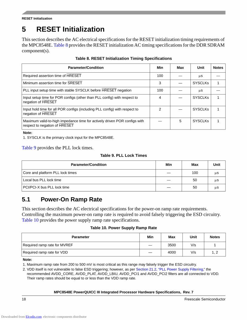
5 RESET InitializationThis section describes the AC electrical specifications for the RESET initialization timing requirements of the MPC8548E. Table 8 provides the RESET initialization AC timing specifications for the DDR SDRAM component(s).
Table 9 provides the PLL lock times.
5.1 Power-On Ramp RateThis section describes the AC electrical specifications for the power-on ramp rate requirements. Controlling the maximum power-on ramp rate is required to avoid falsely triggering the ESD circuitry. Table 10 provides the power supply ramp rate specifications.
Table 8. RESET Initialization Timing Specifications
Parameter/Condition Min Max Unit Notes
Required assertion time of HRESET 100 — μs —
Minimum assertion time for SRESET 3 — SYSCLKs 1
PLL input setup time with stable SYSCLK before HRESET negation 100 — μs —
Input setup time for POR configs (other than PLL config) with respect to negation of HRESET
4 — SYSCLKs 1
Input hold time for all POR configs (including PLL config) with respect to negation of HRESET
2 — SYSCLKs 1
Maximum valid-to-high impedance time for actively driven POR configs with respect to negation of HRESET
— 5 SYSCLKs 1
Note:1. SYSCLK is the primary clock input for the MPC8548E.
Table 9. PLL Lock Times
Parameter/Condition Min Max Unit
Core and platform PLL lock times — 100 μs
Local bus PLL lock time — 50 μs
PCI/PCI-X bus PLL lock time — 50 μs
Table 10. Power Supply Ramp Rate
Parameter Min Max Unit Notes
Required ramp rate for MVREF — 3500 V/s 1
Required ramp rate for VDD — 4000 V/s 1, 2
Note:1. Maximum ramp rate from 200 to 500 mV is most critical as this range may falsely trigger the ESD circuitry. 2. VDD itself is not vulnerable to false ESD triggering; however, as per Section 21.2, “PLL Power Supply Filtering,” the
recommended AVDD_CORE, AVDD_PLAT, AVDD_LBIU, AVDD_PCI1 and AVDD_PCI2 filters are all connected to VDD. Their ramp rates should be equal to or less than the VDD ramp rate.
Downloaded from Elcodis.com electronic components distributor

MPC8548E PowerQUICC III Integrated Processor Hardware Specifications, Rev. 7
Freescale Semiconductor 19
DDR and DDR2 SDRAM
6 DDR and DDR2 SDRAMThis section describes the DC and AC electrical specifications for the DDR SDRAM interface of the MPC8548E. Note that GVDD(typ) = 2.5 V for DDR SDRAM, and GVDD(typ) = 1.8 V for DDR2 SDRAM.
6.1 DDR SDRAM DC Electrical CharacteristicsTable 11 provides the recommended operating conditions for the DDR2 SDRAM controller of the MPC8548E when GVDD(typ) = 1.8 V.
Table 12 provides the DDR2 I/O capacitance when GVDD(typ) = 1.8 V.
Table 11. DDR2 SDRAM DC Electrical Characteristics for GVDD(typ) = 1.8 V
Parameter/Condition Symbol Min Max Unit Notes
I/O supply voltage GVDD 1.71 1.89 V 1
I/O reference voltage MVREF 0.49 × GVDD 0.51 × GVDD V 2
I/O termination voltage VTT MVREF – 0.04 MVREF + 0.04 V 3
Input high voltage VIH MVREF + 0.125 GVDD + 0.3 V —
Input low voltage VIL –0.3 MVREF – 0.125 V —
Output leakage current IOZ –50 50 μA 4
Output high current (VOUT = 1.420 V) IOH –13.4 — mA —
Output low current (VOUT = 0.280 V) IOL 13.4 — mA —
Notes:1. GVDD is expected to be within 50 mV of the DRAM VDD at all times.2. MVREF is expected to be equal to 0.5 × GVDD, and to track GVDD DC variations as measured at the receiver. Peak-to-peak
noise on MVREF may not exceed ±2% of the DC value.3. VTT is not applied directly to the device. It is the supply to which far end signal termination is made and is expected to be
equal to MVREF. This rail should track variations in the DC level of MVREF.4. Output leakage is measured with all outputs disabled, 0 V ≤ VOUT ≤ GVDD.
Table 12. DDR2 SDRAM Capacitance for GVDD(typ)=1.8 V
Parameter/Condition Symbol Min Max Unit Notes
Input/output capacitance: DQ, DQS, DQS CIO 6 8 pF 1
Delta input/output capacitance: DQ, DQS, DQS CDIO — 0.5 pF 1
Note:1. This parameter is sampled. GVDD = 1.8 V ± 0.090 V, f = 1 MHz, TA = 25°C, VOUT = GVDD/2, VOUT (peak-to-peak) = 0.2 V.
Downloaded from Elcodis.com electronic components distributor
MPC8548E PowerQUICC III Integrated Processor Hardware Specifications, Rev. 7
20 Freescale Semiconductor
DDR and DDR2 SDRAM
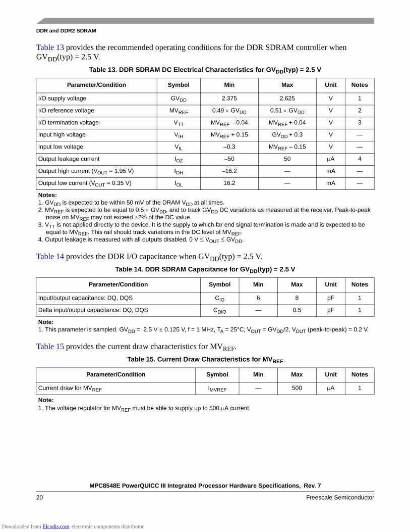
Table 13 provides the recommended operating conditions for the DDR SDRAM controller when GVDD(typ) = 2.5 V.
Table 14 provides the DDR I/O capacitance when GVDD(typ) = 2.5 V.
Table 15 provides the current draw characteristics for MVREF.
Table 13. DDR SDRAM DC Electrical Characteristics for GVDD(typ) = 2.5 V
Parameter/Condition Symbol Min Max Unit Notes
I/O supply voltage GVDD 2.375 2.625 V 1
I/O reference voltage MVREF 0.49 × GVDD 0.51 × GVDD V 2
I/O termination voltage VTT MVREF – 0.04 MVREF + 0.04 V 3
Input high voltage VIH MVREF + 0.15 GVDD + 0.3 V —
Input low voltage VIL –0.3 MVREF – 0.15 V —
Output leakage current IOZ –50 50 μA 4
Output high current (VOUT = 1.95 V) IOH –16.2 — mA —
Output low current (VOUT = 0.35 V) IOL 16.2 — mA —
Notes:1. GVDD is expected to be within 50 mV of the DRAM VDD at all times.2. MVREF is expected to be equal to 0.5 × GVDD, and to track GVDD DC variations as measured at the receiver. Peak-to-peak
noise on MVREF may not exceed ±2% of the DC value.3. VTT is not applied directly to the device. It is the supply to which far end signal termination is made and is expected to be
equal to MVREF. This rail should track variations in the DC level of MVREF.4. Output leakage is measured with all outputs disabled, 0 V ≤ VOUT ≤ GVDD.
Table 14. DDR SDRAM Capacitance for GVDD(typ) = 2.5 V
Parameter/Condition Symbol Min Max Unit Notes
Input/output capacitance: DQ, DQS CIO 6 8 pF 1
Delta input/output capacitance: DQ, DQS CDIO — 0.5 pF 1
Note:1. This parameter is sampled. GVDD = 2.5 V ± 0.125 V, f = 1 MHz, TA = 25°C, VOUT = GVDD/2, VOUT (peak-to-peak) = 0.2 V.
Table 15. Current Draw Characteristics for MVREF
Parameter/Condition Symbol Min Max Unit Notes
Current draw for MVREF IMVREF — 500 μA 1
Note: 1. The voltage regulator for MVREF must be able to supply up to 500 μA current.
Downloaded from Elcodis.com electronic components distributor

MPC8548E PowerQUICC III Integrated Processor Hardware Specifications, Rev. 7
Freescale Semiconductor 21
DDR and DDR2 SDRAM
6.2 DDR SDRAM AC Electrical CharacteristicsThis section provides the AC electrical characteristics for the DDR SDRAM interface. The DDR controller supports both DDR1 and DDR2 memories. DDR1 is supported with the following AC timings at data rates of 333 MHz. DDR2 is supported with the following AC timings at data rates down to 333 MHz.
6.2.1 DDR SDRAM Input AC Timing SpecificationsTable 16 provides the input AC timing specifications for the DDR SDRAM when GVDD(typ) = 1.8 V.
Table 17 provides the input AC timing specifications for the DDR SDRAM when GVDD(typ) = 2.5 V.
Table 18 provides the input AC timing specifications for the DDR SDRAM interface.
Table 16. DDR2 SDRAM Input AC Timing Specifications for 1.8-V InterfaceAt recommended operating conditions
Parameter Symbol Min Max Unit
AC input low voltage VIL — MVREF – 0.25 V
AC input high voltage VIH MVREF + 0.25 — V
Table 17. DDR SDRAM Input AC Timing Specifications for 2.5-V InterfaceAt recommended operating conditions.
Parameter Symbol Min Max Unit
AC input low voltage VIL — MVREF – 0.31 V
AC input high voltage VIH MVREF + 0.31 — V
Table 18. DDR SDRAM Input AC Timing SpecificationsAt recommended operating conditions.
Parameter Symbol Min Max Unit Notes
Controller Skew for MDQS—MDQ/MECC533 MHz400 MHz333 MHz
tCISKEW
–300–365–390
300365390
ps 1, 2
Notes:1. tCISKEW represents the total amount of skew consumed by the controller between MDQS[n] and any corresponding bit that
is captured with MDQS[n]. This should be subtracted from the total timing budget.2. The amount of skew that can be tolerated from MDQS to a corresponding MDQ signal is called tDISKEW. This can be
determined by the following equation: tDISKEW = ± (T/4 – abs(tCISKEW)) where T is the clock period and abs(tCISKEW) is the absolute value of tCISKEW.
Downloaded from Elcodis.com electronic components distributor
MPC8548E PowerQUICC III Integrated Processor Hardware Specifications, Rev. 7
22 Freescale Semiconductor
DDR and DDR2 SDRAM
6.2.2 DDR SDRAM Output AC Timing SpecificationsTable 19. DDR SDRAM Output AC Timing Specifications
At recommended operating conditions.
Parameter Symbol1 Min Max Unit Notes
MCK[n] cycle time, MCK[n]/MCK[n] crossing tMCK 3.75 6 ns 2
ADDR/CMD output setup with respect to MCK533 MHz400 MHz333 MHz
tDDKHAS
1.481.952.40
———
ns 3
ADDR/CMD output hold with respect to MCK533 MHz400 MHz333 MHz
tDDKHAX
1.481.952.40
———
ns 3
MCS[n] output setup with respect to MCK533 MHz400 MHz333 MHz
tDDKHCS
1.481.952.40
———
ns 3
MCS[n] output hold with respect to MCK533 MHz400 MHz333 MHz
tDDKHCX
1.481.952.40
———
ns 3
MCK to MDQS Skew tDDKHMH –0.6 0.6 ns 4
MDQ/MECC/MDM output setup with respect to MDQS
533 MHz400 MHz333 MHz
tDDKHDS,tDDKLDS
538700900
———
ps 5
MDQ/MECC/MDM output hold with respect to MDQS
533 MHz400 MHz333 MHz
tDDKHDX,tDDKLDX
538700900
———
ps 5
MDQS preamble start tDDKHMP –0.5 × tMCK – 0.6 –0.5 × tMCK + 0.6 ns 6
Downloaded from Elcodis.com electronic components distributor
MPC8548E PowerQUICC III Integrated Processor Hardware Specifications, Rev. 7
Freescale Semiconductor 23
DDR and DDR2 SDRAM
NOTEFor the ADDR/CMD setup and hold specifications in Table 19, it is assumed that the clock control register is set to adjust the memory clocks by 1/2 applied cycle.
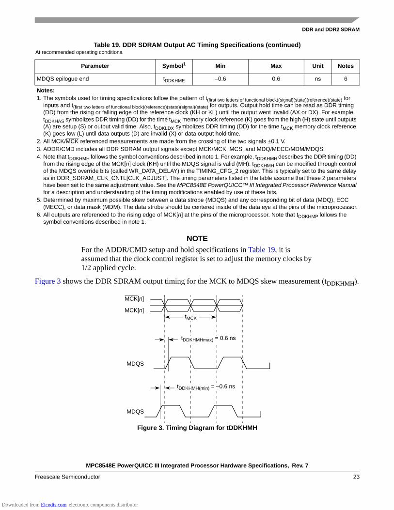
Figure 3 shows the DDR SDRAM output timing for the MCK to MDQS skew measurement (tDDKHMH).
Figure 3. Timing Diagram for tDDKHMH
MDQS epilogue end tDDKHME –0.6 0.6 ns 6
Notes:1. The symbols used for timing specifications follow the pattern of t(first two letters of functional block)(signal)(state)(reference)(state) for
inputs and t(first two letters of functional block)(reference)(state)(signal)(state) for outputs. Output hold time can be read as DDR timing (DD) from the rising or falling edge of the reference clock (KH or KL) until the output went invalid (AX or DX). For example, tDDKHAS symbolizes DDR timing (DD) for the time tMCK memory clock reference (K) goes from the high (H) state until outputs (A) are setup (S) or output valid time. Also, tDDKLDX symbolizes DDR timing (DD) for the time tMCK memory clock reference (K) goes low (L) until data outputs (D) are invalid (X) or data output hold time.
2. All MCK/MCK referenced measurements are made from the crossing of the two signals ±0.1 V.3. ADDR/CMD includes all DDR SDRAM output signals except MCK/MCK, MCS, and MDQ/MECC/MDM/MDQS.4. Note that tDDKHMH follows the symbol conventions described in note 1. For example, tDDKHMH describes the DDR timing (DD)
from the rising edge of the MCK[n] clock (KH) until the MDQS signal is valid (MH). tDDKHMH can be modified through control of the MDQS override bits (called WR_DATA_DELAY) in the TIMING_CFG_2 register. This is typically set to the same delay as in DDR_SDRAM_CLK_CNTL[CLK_ADJUST]. The timing parameters listed in the table assume that these 2 parameters have been set to the same adjustment value. See the MPC8548E PowerQUICC™ III Integrated Processor Reference Manual for a description and understanding of the timing modifications enabled by use of these bits.
5. Determined by maximum possible skew between a data strobe (MDQS) and any corresponding bit of data (MDQ), ECC (MECC), or data mask (MDM). The data strobe should be centered inside of the data eye at the pins of the microprocessor.
6. All outputs are referenced to the rising edge of MCK[n] at the pins of the microprocessor. Note that tDDKHMP follows the symbol conventions described in note 1.
Table 19. DDR SDRAM Output AC Timing Specifications (continued)At recommended operating conditions.
Parameter Symbol1 Min Max Unit Notes
tDDKHMHmax) = 0.6 ns
MDQS
MCK[n]
MCK[n]tMCK
tDDKHMH(min) = –0.6 ns
MDQS
Downloaded from Elcodis.com electronic components distributor

MPC8548E PowerQUICC III Integrated Processor Hardware Specifications, Rev. 7
24 Freescale Semiconductor
DDR and DDR2 SDRAM
Figure 4 shows the DDR SDRAM output timing diagram.+
Figure 4. DDR SDRAM Output Timing Diagram
Figure 5 provides the AC test load for the DDR bus.
Figure 5. DDR AC Test Load
ADDR/CMD
tDDKHAS, tDDKHCS
tDDKLDS
tDDKHDS
MDQ[x]
MDQS[n]
MCK[n]
MCK[n]tMCK
tDDKLDX
tDDKHDX
D1D0
tDDKHAX, tDDKHCX
Write A0 NOOP
tDDKHME
tDDKHMP
tDDKHMH
Output Z0 = 50 Ω GVDD/2RL = 50 Ω
Downloaded from Elcodis.com electronic components distributor
MPC8548E PowerQUICC III Integrated Processor Hardware Specifications, Rev. 7
Freescale Semiconductor 25
DUART
7 DUARTThis section describes the DC and AC electrical specifications for the DUART interface of the MPC8548E.
7.1 DUART DC Electrical CharacteristicsTable 20 provides the DC electrical characteristics for the DUART interface.
7.2 DUART AC Electrical SpecificationsTable 21 provides the AC timing parameters for the DUART interface.
Table 20. DUART DC Electrical Characteristics
Parameter Symbol Min Max Unit
High-level input voltage VIH 2 OVDD + 0.3 V
Low-level input voltage VIL –0.3 0.8 V
Input current (VIN1 = 0 V or VIN = VDD) IIN — ±5 μA
High-level output voltage (OVDD = min, IOH = –2 mA) VOH 2.4 — V
Low-level output voltage (OVDD = min, IOL = 2 mA) VOL — 0.4 V
Note:1. Note that the symbol VIN, in this case, represents the OVIN symbol referenced in Table 1 and Table 2.
Table 21. DUART AC Timing Specifications
Parameter Value Unit Notes
Minimum baud rate fCCB/1,048,576 baud 1, 2
Maximum baud rate fCCB/16 baud 1, 2, 3
Oversample rate 16 — 1, 4
Notes:1. Guaranteed by design.2. fCCB refers to the internal platform clock.3. Actual attainable baud rate is limited by the latency of interrupt processing.4. The middle of a start bit is detected as the 8th sampled 0 after the 1-to-0 transition of the start bit. Subsequent bit values are
sampled each 16th sample.
Downloaded from Elcodis.com electronic components distributor
MPC8548E PowerQUICC III Integrated Processor Hardware Specifications, Rev. 7
26 Freescale Semiconductor
Enhanced Three-Speed Ethernet (eTSEC)
8 Enhanced Three-Speed Ethernet (eTSEC)This section provides the AC and DC electrical characteristics for the enhanced three-speed Ethernet controller. The electrical characteristics for MDIO and MDC are specified in Section 9, “Ethernet Management Interface Electrical Characteristics.”
8.1 Enhanced Three-Speed Ethernet Controller (eTSEC) (10/100/1Gb Mbps)—GMII/MII/TBI/RGMII/RTBI/RMII Electrical Characteristics
The electrical characteristics specified here apply to all gigabit media independent interface (GMII), media independent interface (MII), ten-bit interface (TBI), reduced gigabit media independent interface (RGMII), reduced ten-bit interface (RTBI), and reduced media independent interface (RMII) signals except management data input/output (MDIO) and management data clock (MDC). The RGMII and RTBI interfaces are defined for 2.5 V, while the GMII, MII, and TBI interfaces can be operated at 3.3 or 2.5 V. The GMII, MII, or TBI interface timing is compliant with the IEEE 802.3. The RGMII and RTBI interfaces follow the Reduced Gigabit Media-Independent Interface (RGMII) Specification Version 1.3 (12/10/2000). The RMII interface follows the RMII Consortium RMII Specification Version 1.2 (3/20/1998). The electrical characteristics for MDIO and MDC are specified in Section 9, “Ethernet Management Interface Electrical Characteristics.”
8.1.1 eTSEC DC Electrical CharacteristicsAll GMII, MII, TBI, RGMII, RMII, and RTBI drivers and receivers comply with the DC parametric attributes specified in Table 22 and Table 23. The RGMII and RTBI signals are based on a 2.5-V CMOS interface voltage as defined by JEDEC EIA/JESD8-5.
Table 22. GMII, MII, RMII, and TBI DC Electrical Characteristics
Parameter Symbol Min Max Unit Notes
Supply voltage 3.3 V LVDDTVDD
3.13 3.47 V 1, 2
Output high voltage (LVDD/TVDD = min, IOH = –4.0 mA) VOH 2.40 LVDD/TVDD + 0.3 V —
Output low voltage (LVDD/TVDD = min, IOL = 4.0 mA) VOL GND 0.50 V —
Input high voltage VIH 2.0 LVDD/TVDD + 0.3 V —
Input low voltage VIL –0.3 0.90 V —
Input high current (VIN = LVDD, VIN = TVDD) IIH — 40 μA 1, 2, 3
Input low current (VIN = GND) IIL –600 — μA —
Notes:1. LVDD supports eTSECs 1 and 2.2. TVDD supports eTSECs 3 and 4.3. The symbol VIN, in this case, represents the LVIN and TVIN symbols referenced in Table 1 and Table 2.
Downloaded from Elcodis.com electronic components distributor

MPC8548E PowerQUICC III Integrated Processor Hardware Specifications, Rev. 7
Freescale Semiconductor 27
Enhanced Three-Speed Ethernet (eTSEC)
8.2 FIFO, GMII, MII, TBI, RGMII, RMII, and RTBI AC Timing Specifications
The AC timing specifications for FIFO, GMII, MII, TBI, RGMII, RMII, and RTBI are presented in this section.
8.2.1 FIFO AC SpecificationsThe basis for the AC specifications for the eTSEC’s FIFO modes is the double data rate RGMII and RTBI specifications, since they have similar performances and are described in a source-synchronous fashion like FIFO modes. However, the FIFO interface provides deliberate skew between the transmitted data and source clock in GMII fashion.
When the eTSEC is configured for FIFO modes, all clocks are supplied from external sources to the relevant eTSEC interface. That is, the transmit clock must be applied to the eTSECn’s TSECn_TX_CLK, while the receive clock must be applied to pin TSECn_RX_CLK. The eTSEC internally uses the transmit clock to synchronously generate transmit data and outputs an echoed copy of the transmit clock back out onto the TSECn_GTX_CLK pin (while transmit data appears on TSECn_TXD[7:0], for example). It is intended that external receivers capture eTSEC transmit data using the clock on TSECn_GTX_CLK as a source- synchronous timing reference. Typically, the clock edge that launched the data can be used, since the clock is delayed by the eTSEC to allow acceptable set-up margin at the receiver. Note that there is relationship between the maximum FIFO speed and the platform speed. For more information see Section 4.5, “Platform to FIFO Restrictions.”
Table 23. GMII, MII, RMII, TBI, RGMII, RTBI, and FIFO DC Electrical Characteristics
Parameters Symbol Min Max Unit Notes
Supply voltage 2.5 V LVDD/TVDD 2.37 2.63 V 1, 2
Output high voltage (LVDD/TVDD = Min, IOH = –1.0 mA)
VOH 2.00 LVDD/TVDD + 0.3 V —
Output low voltage (LVDD/TVDD = Min, IOL = 1.0 mA)
VOL GND –0.3 0.40 V —
Input high voltage VIH 1.70 LVDD/TVDD + 0.3 V —
Input low voltage VIL –0.3 0.90 V —
Input high current (VIN = LVDD, VIN = TVDD) IIH — 10 μA 1, 2, 3
Input low current (VIN = GND) IIL –15 — μA 3
Notes:1. LVDD supports eTSECs 1 and 2.2. TVDD supports eTSECs 3 and 4.3. Note that the symbol VIN, in this case, represents the LVIN and TVIN symbols referenced in Table 1 and Table 2.
Downloaded from Elcodis.com electronic components distributor

MPC8548E PowerQUICC III Integrated Processor Hardware Specifications, Rev. 7
28 Freescale Semiconductor
Enhanced Three-Speed Ethernet (eTSEC)
A summary of the FIFO AC specifications appears in Table 24 and Table 25.
Timing diagrams for FIFO appear in Figure 6 and Figure 7.
Figure 6. FIFO Transmit AC Timing Diagram
Table 24. FIFO Mode Transmit AC Timing Specification
Parameter/Condition Symbol Min Typ Max Unit
TX_CLK, GTX_CLK clock period tFIT 5.3 8.0 100 ns
TX_CLK, GTX_CLK duty cycle tFITH/tFIT 45 50 55 %
TX_CLK, GTX_CLK peak-to-peak jitter tFITJ — — 250 ps
Rise time TX_CLK (20%–80%) tFITR — — 0.75 ns
Fall time TX_CLK (80%–20%) tFITF — — 0.75 ns
FIFO data TXD[7:0], TX_ER, TX_EN setup time to GTX_CLK tFITDV 2.0 — — ns
GTX_CLK to FIFO data TXD[7:0], TX_ER, TX_EN hold time tFITDX 0.5 — 3.0 ns
Table 25. FIFO Mode Receive AC Timing Specification
Parameter/Condition Symbol Min Typ Max Unit
RX_CLK clock period tFIR 5.3 8.0 100 ns
RX_CLK duty cycle tFIRH/tFIR 45 50 55 %
RX_CLK peak-to-peak jitter tFIRJ — — 250 ps
Rise time RX_CLK (20%–80%) tFIRR — — 0.75 ns
Fall time RX_CLK (80%–20%) tFIRF — — 0.75 ns
RXD[7:0], RX_DV, RX_ER setup time to RX_CLK tFIRDV 1.5 — — ns
RXD[7:0], RX_DV, RX_ER hold time to RX_CLK tFIRDX 0.5 — — ns
Note: 1. The minimum cycle period of the TX_CLK and RX_CLK is dependent on the maximum platform frequency of t he speed bins
the part belongs to as well as the FIFO mode under operation. Refer to Section 4.5, “Platform to FIFO Restrictions.”
tFIT
tFITH
tFITF
TXD[7:0]TX_EN
GTX_CLK
TX_ER
tFITR
tFITDV tFITDX
Downloaded from Elcodis.com electronic components distributor
MPC8548E PowerQUICC III Integrated Processor Hardware Specifications, Rev. 7
Freescale Semiconductor 29
Enhanced Three-Speed Ethernet (eTSEC)
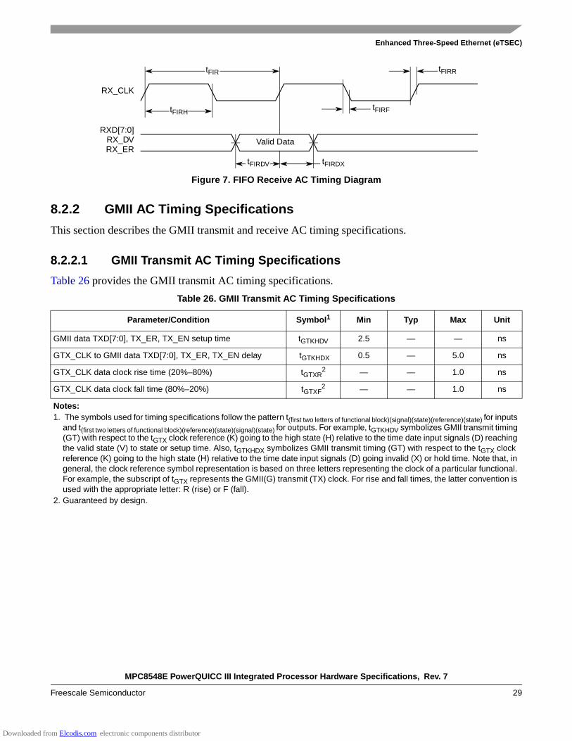
Figure 7. FIFO Receive AC Timing Diagram
8.2.2 GMII AC Timing Specifications
This section describes the GMII transmit and receive AC timing specifications.
8.2.2.1 GMII Transmit AC Timing Specifications
Table 26 provides the GMII transmit AC timing specifications.Table 26. GMII Transmit AC Timing Specifications
Parameter/Condition Symbol1 Min Typ Max Unit
GMII data TXD[7:0], TX_ER, TX_EN setup time tGTKHDV 2.5 — — ns
GTX_CLK to GMII data TXD[7:0], TX_ER, TX_EN delay tGTKHDX 0.5 — 5.0 ns
GTX_CLK data clock rise time (20%–80%) tGTXR2 — — 1.0 ns
GTX_CLK data clock fall time (80%–20%) tGTXF2 — — 1.0 ns
Notes:1. The symbols used for timing specifications follow the pattern t(first two letters of functional block)(signal)(state)(reference)(state) for inputs
and t(first two letters of functional block)(reference)(state)(signal)(state) for outputs. For example, tGTKHDV symbolizes GMII transmit timing (GT) with respect to the tGTX clock reference (K) going to the high state (H) relative to the time date input signals (D) reaching the valid state (V) to state or setup time. Also, tGTKHDX symbolizes GMII transmit timing (GT) with respect to the tGTX clock reference (K) going to the high state (H) relative to the time date input signals (D) going invalid (X) or hold time. Note that, in general, the clock reference symbol representation is based on three letters representing the clock of a particular functional. For example, the subscript of tGTX represents the GMII(G) transmit (TX) clock. For rise and fall times, the latter convention is used with the appropriate letter: R (rise) or F (fall).
2. Guaranteed by design.
tFIR
tFIRHtFIRF
tFIRR
RX_CLK
RXD[7:0]RX_DVRX_ER
Valid Data
tFIRDV tFIRDX
Downloaded from Elcodis.com electronic components distributor

MPC8548E PowerQUICC III Integrated Processor Hardware Specifications, Rev. 7
30 Freescale Semiconductor
Enhanced Three-Speed Ethernet (eTSEC)
Figure 8 shows the GMII transmit AC timing diagram.
Figure 8. GMII Transmit AC Timing Diagram
8.2.2.2 GMII Receive AC Timing Specifications
Table 27 provides the GMII receive AC timing specifications.
Figure 9 provides the AC test load for eTSEC.
Figure 9. eTSEC AC Test Load
Table 27. GMII Receive AC Timing Specifications
Parameter/Condition Symbol1 Min Typ Max Unit
RX_CLK clock period tGRX — 8.0 — ns
RX_CLK duty cycle tGRXH/tGRX 35 — 75 ns
RXD[7:0], RX_DV, RX_ER setup time to RX_CLK tGRDVKH 2.0 — — ns
RXD[7:0], RX_DV, RX_ER hold time to RX_CLK tGRDXKH 0 — — ns
RX_CLK clock rise (20%-80%) tGRXR2 — — 1.0 ns
RX_CLK clock fall time (80%-20%) tGRXF2 — — 1.0 ns
Notes:1. The symbols used for timing specifications follow the pattern of t(first two letters of functional block)(signal)(state)(reference)(state) for
inputs and t(first two letters of functional block)(reference)(state)(signal)(state) for outputs. For example, tGRDVKH symbolizes GMII receive timing (GR) with respect to the time data input signals (D) reaching the valid state (V) relative to the tRX clock reference (K) going to the high state (H) or setup time. Also, tGRDXKL symbolizes GMII receive timing (GR) with respect to the time data input signals (D) went invalid (X) relative to the tGRX clock reference (K) going to the low (L) state or hold time. Note that, in general, the clock reference symbol representation is based on three letters representing the clock of a particular functional. For example, the subscript of tGRX represents the GMII (G) receive (RX) clock. For rise and fall times, the latter convention is used with the appropriate letter: R (rise) or F (fall).
2. Guaranteed by design.
GTX_CLK
TXD[7:0]
tGTKHDX
tGTX
tGTXH
tGTXR
tGTXF
tGTKHDV
TX_ENTX_ER
Output Z0 = 50 Ω LVDD/2RL = 50 Ω
Downloaded from Elcodis.com electronic components distributor

MPC8548E PowerQUICC III Integrated Processor Hardware Specifications, Rev. 7
Freescale Semiconductor 31
Enhanced Three-Speed Ethernet (eTSEC)
Figure 10 shows the GMII receive AC timing diagram.
Figure 10. GMII Receive AC Timing Diagram
8.2.3 MII AC Timing SpecificationsThis section describes the MII transmit and receive AC timing specifications.
8.2.3.1 MII Transmit AC Timing Specifications
Table 28 provides the MII transmit AC timing specifications.Table 28. MII Transmit AC Timing Specifications
Parameter/Condition Symbol1 Min Typ Max Unit
TX_CLK clock period 10 Mbps tMTX2 — 400 — ns
TX_CLK clock period 100 Mbps tMTX — 40 — ns
TX_CLK duty cycle tMTXH/tMTX 35 — 65 %
TX_CLK to MII data TXD[3:0], TX_ER, TX_EN delay tMTKHDX 1 5 15 ns
TX_CLK data clock rise (20%–80%) tMTXR2 1.0 — 4.0 ns
TX_CLK data clock fall (80%–20%) tMTXF2 1.0 — 4.0 ns
Notes:1. The symbols used for timing specifications follow the pattern of t(first two letters of functional block)(signal)(state)(reference)(state) for
inputs and t(first two letters of functional block)(reference)(state)(signal)(state) for outputs. For example, tMTKHDX symbolizes MII transmit timing (MT) for the time tMTX clock reference (K) going high (H) until data outputs (D) are invalid (X). Note that, in general, the clock reference symbol representation is based on two to three letters representing the clock of a particular functional. For example, the subscript of tMTX represents the MII(M) transmit (TX) clock. For rise and fall times, the latter convention is used with the appropriate letter: R (rise) or F (fall).
2. Guaranteed by design.
RX_CLK
RXD[7:0]
tGRDXKH
tGRX
tGRXH
tGRXR
tGRXF
tGRDVKH
RX_DVRX_ER
Downloaded from Elcodis.com electronic components distributor
MPC8548E PowerQUICC III Integrated Processor Hardware Specifications, Rev. 7
32 Freescale Semiconductor
Enhanced Three-Speed Ethernet (eTSEC)
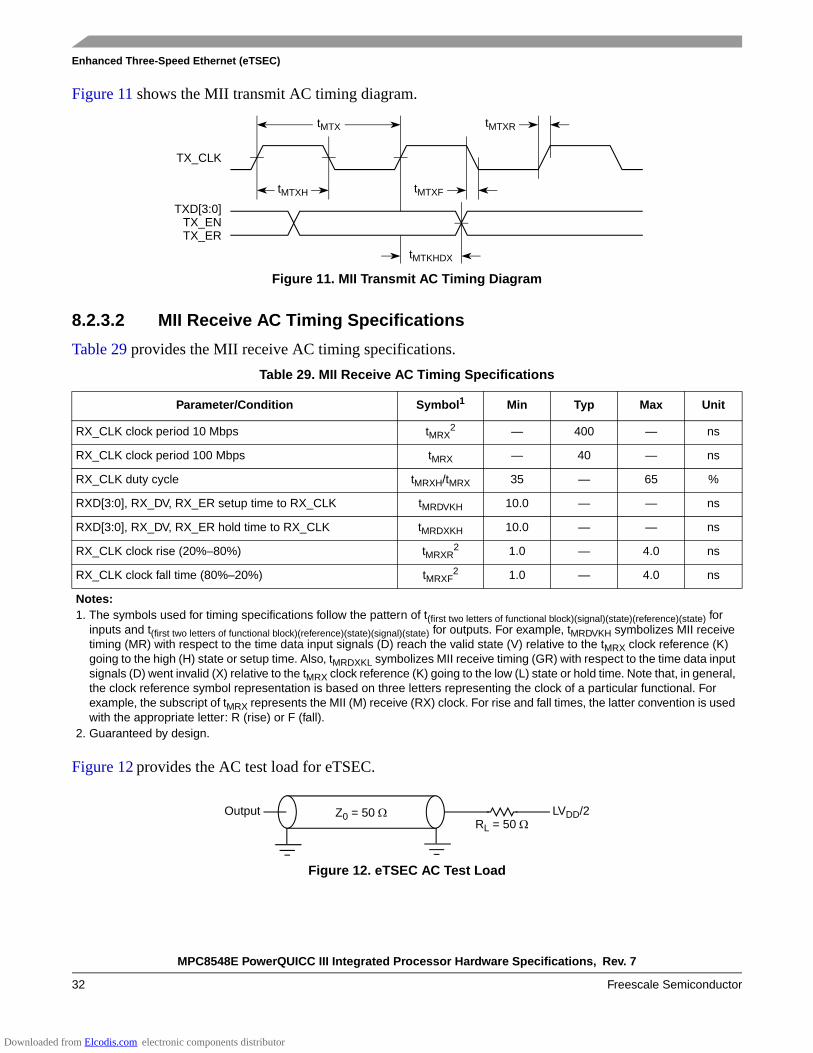
Figure 11 shows the MII transmit AC timing diagram.
Figure 11. MII Transmit AC Timing Diagram
8.2.3.2 MII Receive AC Timing Specifications
Table 29 provides the MII receive AC timing specifications.
Figure 12 provides the AC test load for eTSEC.
Figure 12. eTSEC AC Test Load
Table 29. MII Receive AC Timing Specifications
Parameter/Condition Symbol1 Min Typ Max Unit
RX_CLK clock period 10 Mbps tMRX2 — 400 — ns
RX_CLK clock period 100 Mbps tMRX — 40 — ns
RX_CLK duty cycle tMRXH/tMRX 35 — 65 %
RXD[3:0], RX_DV, RX_ER setup time to RX_CLK tMRDVKH 10.0 — — ns
RXD[3:0], RX_DV, RX_ER hold time to RX_CLK tMRDXKH 10.0 — — ns
RX_CLK clock rise (20%–80%) tMRXR2 1.0 — 4.0 ns
RX_CLK clock fall time (80%–20%) tMRXF2 1.0 — 4.0 ns
Notes:1. The symbols used for timing specifications follow the pattern of t(first two letters of functional block)(signal)(state)(reference)(state) for
inputs and t(first two letters of functional block)(reference)(state)(signal)(state) for outputs. For example, tMRDVKH symbolizes MII receive timing (MR) with respect to the time data input signals (D) reach the valid state (V) relative to the tMRX clock reference (K) going to the high (H) state or setup time. Also, tMRDXKL symbolizes MII receive timing (GR) with respect to the time data input signals (D) went invalid (X) relative to the tMRX clock reference (K) going to the low (L) state or hold time. Note that, in general, the clock reference symbol representation is based on three letters representing the clock of a particular functional. For example, the subscript of tMRX represents the MII (M) receive (RX) clock. For rise and fall times, the latter convention is used with the appropriate letter: R (rise) or F (fall).
2. Guaranteed by design.
TX_CLK
TXD[3:0]
tMTKHDX
tMTX
tMTXH
tMTXR
tMTXF
TX_ENTX_ER
Output Z0 = 50 Ω LVDD/2RL = 50 Ω
Downloaded from Elcodis.com electronic components distributor

MPC8548E PowerQUICC III Integrated Processor Hardware Specifications, Rev. 7
Freescale Semiconductor 33
Enhanced Three-Speed Ethernet (eTSEC)
Figure 13 shows the MII receive AC timing diagram.
Figure 13. MII Receive AC Timing Diagram
8.2.4 TBI AC Timing SpecificationsThis section describes the TBI transmit and receive AC timing specifications.
8.2.4.1 TBI Transmit AC Timing Specifications
Table 30 provides the TBI transmit AC timing specifications.Table 30. TBI Transmit AC Timing Specifications
Parameter/Condition Symbol1 Min Typ Max Unit
TCG[9:0] setup time GTX_CLK going high tTTKHDV 2.0 — — ns
TCG[9:0] hold time from GTX_CLK going high tTTKHDX 1.0 — — ns
GTX_CLK rise (20%–80%) tTTXR2 — — 1.0 ns
GTX_CLK fall time (80%–20%) tTTXF2 — — 1.0 ns
Notes:1. The symbols used for timing specifications follow the pattern of t(first two letters of functional block)(signal)(state )(reference)(state) for
inputs and t(first two letters of functional block)(reference)(state)(signal)(state) for outputs. For example, tTTKHDV symbolizes the TBI transmit timing (TT) with respect to the time from tTTX (K) going high (H) until the referenced data signals (D) reach the valid state (V) or setup time. Also, tTTKHDX symbolizes the TBI transmit timing (TT) with respect to the time from tTTX (K) going high (H) until the referenced data signals (D) reach the invalid state (X) or hold time. Note that, in general, the clock reference symbol representation is based on three letters representing the clock of a particular functional. For example, the subscript of tTTX represents the TBI (T) transmit (TX) clock. For rise and fall times, the latter convention is used with the appropriate letter: R (rise) or F (fall).
2. Guaranteed by design.
RX_CLK
RXD[3:0]
tMRDXKL
tMRX
tMRXH
tMRXR
tMRXF
RX_DVRX_ER
tMRDVKH
Valid Data
Downloaded from Elcodis.com electronic components distributor

MPC8548E PowerQUICC III Integrated Processor Hardware Specifications, Rev. 7
34 Freescale Semiconductor
Enhanced Three-Speed Ethernet (eTSEC)
Figure 14 shows the TBI transmit AC timing diagram.
Figure 14. TBI Transmit AC Timing Diagram
8.2.4.2 TBI Receive AC Timing Specifications
Table 31 provides the TBI receive AC timing specifications.Table 31. TBI Receive AC Timing Specifications
Parameter/Condition Symbol1 Min Typ Max Unit
TSECn_RX_CLK[0:1] clock period tTRX — 16.0 — ns
TSECn_RX_CLK[0:1] skew tSKTRX 7.5 — 8.5 ns
TSECn_RX_CLK[0:1] duty cycle tTRXH/tTRX 40 — 60 %
RCG[9:0] setup time to rising TSECn_RX_CLK tTRDVKH 2.5 — — ns
RCG[9:0] hold time to rising TSECn_RX_CLK tTRDXKH 1.5 — — ns
TSECn_RX_CLK[0:1] clock rise time (20%–80%) tTRXR2 0.7 — 2.4 ns
TSECn_RX_CLK[0:1] clock fall time (80%–20%) tTRXF2 0.7 — 2.4 ns
Notes:1. The symbols used for timing specifications follow the pattern of t(first two letters of functional block)(signal)(state)(reference)(state) for
inputs and t(first two letters of functional block)(reference)(state)(signal)(state) for outputs. For example, tTRDVKH symbolizes TBI receive timing (TR) with respect to the time data input signals (D) reach the valid state (V) relative to the tTRX clock reference (K) going to the high (H) state or setup time. Also, tTRDXKH symbolizes TBI receive timing (TR) with respect to the time data input signals (D) went invalid (X) relative to the tTRX clock reference (K) going to the high (H) state. Note that, in general, the clock reference symbol representation is based on three letters representing the clock of a particular functional. For example, the subscript of tTRX represents the TBI (T) receive (RX) clock. For rise and fall times, the latter convention is used with the appropriate letter: R (rise) or F (fall). For symbols representing skews, the subscript is skew (SK) followed by the clock that is being skewed (TRX).
2. Guaranteed by design.
GTX_CLK
TCG[9:0]
tTTXR
tTTX
tTTXH
tTTXR
tTTXF
tTTKHDV
tTTKHDX
tTTXF
Downloaded from Elcodis.com electronic components distributor

MPC8548E PowerQUICC III Integrated Processor Hardware Specifications, Rev. 7
Freescale Semiconductor 35
Enhanced Three-Speed Ethernet (eTSEC)
Figure 15 shows the TBI receive AC timing diagram.
Figure 15. TBI Receive AC Timing Diagram
8.2.5 TBI Single-Clock Mode AC SpecificationsWhen the eTSEC is configured for TBI modes, all clocks are supplied from external sources to the relevant eTSEC interface. In single-clock TBI mode, when TBICON[CLKSEL] = 1, a 125-MHz TBI receive clock is supplied on the TSECn_RX_CLK pin (no receive clock is used on TSECn_TX_CLK in this mode, whereas for the dual-clock mode this is the PMA1 receive clock). The 125-MHz transmit clock is applied on the TSEC_GTX_CLK125 pin in all TBI modes.
A summary of the single-clock TBI mode AC specifications for receive appears in Table 32.Table 32. TBI single-clock Mode Receive AC Timing Specification
Parameter/Condition Symbol Min Typ Max Unit
RX_CLK clock period tTRRX 7.5 8.0 8.5 ns
RX_CLK duty cycle tTRRH/TRRX 40 50 60 %
RX_CLK peak-to-peak jitter tTRRJ — — 250 ps
Rise time RX_CLK (20%–80%) tTRRR — — 1.0 ns
Fall time RX_CLK (80%–20%) tTRRF — — 1.0 ns
RCG[9:0] setup time to RX_CLK rising edge tTRRDVKH 2.0 — — ns
RCG[9:0] hold time to RX_CLK rising edge tTRRDXKH 1.0 — — ns
TSECn_RX_CLK1
RCG[9:0]
tTRX
tTRXH
tTRXR
tTRXF
tTRDVKH
TSECn_RX_CLK0
tTRDXKH
tTRDVKH
tTRDXKH
tSKTRX
tTRXH
Valid Data Valid Data
Downloaded from Elcodis.com electronic components distributor
MPC8548E PowerQUICC III Integrated Processor Hardware Specifications, Rev. 7
36 Freescale Semiconductor
Enhanced Three-Speed Ethernet (eTSEC)
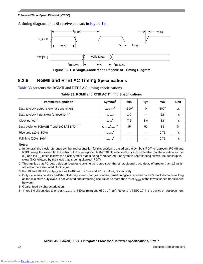
A timing diagram for TBI receive appears in Figure 16..
Figure 16. TBI Single-Clock Mode Receive AC Timing Diagram
8.2.6 RGMII and RTBI AC Timing Specifications
Table 33 presents the RGMII and RTBI AC timing specifications.Table 33. RGMII and RTBI AC Timing Specifications
Parameter/Condition Symbol1 Min Typ Max Unit
Data to clock output skew (at transmitter) tSKRGT5 –5006 0 5006 ps
Data to clock input skew (at receiver) 2 tSKRGT 1.0 — 2.8 ns
Clock period 3 tRGT5 7.2 8.0 8.8 ns
Duty cycle for 10BASE-T and 100BASE-TX3, 4 tRGTH/tRGT5 45 50 55 %
Rise time (20%–80%) tRGTR5 — — 0.75 ns
Fall time (20%–80%) tRGTF5 — — 0.75 ns
Notes:1. In general, the clock reference symbol representation for this section is based on the symbols RGT to represent RGMII and
RTBI timing. For example, the subscript of tRGT represents the TBI (T) receive (RX) clock. Note also that the notation for rise (R) and fall (F) times follows the clock symbol that is being represented. For symbols representing skews, the subscript is skew (SK) followed by the clock that is being skewed (RGT).
2. This implies that PC board design requires clocks to be routed such that an additional trace delay of greater than 1.5 ns is added to the associated clock signal.
3. For 10 and 100 Mbps, tRGT scales to 400 ns ± 40 ns and 40 ns ± 4 ns, respectively.4. Duty cycle may be stretched/shrunk during speed changes or while transitioning to a received packet's clock domains as long
as the minimum duty cycle is not violated and stretching occurs for no more than three tRGT of the lowest speed transitioned between.
5. Guaranteed by characterization.6. In rev 1.0 silicon, due to errata, tSKRGT is -650 ps (min) and 650 ps (max). Refer to “eTSEC 10” in the device errata document.
tTRRX
tTRRH tTRRF
tTRRR
RX_CLK
RCG[9:0] Valid Data
tTRRDXKHtTRRDVKH
Downloaded from Elcodis.com electronic components distributor
MPC8548E PowerQUICC III Integrated Processor Hardware Specifications, Rev. 7
Freescale Semiconductor 37
Enhanced Three-Speed Ethernet (eTSEC)
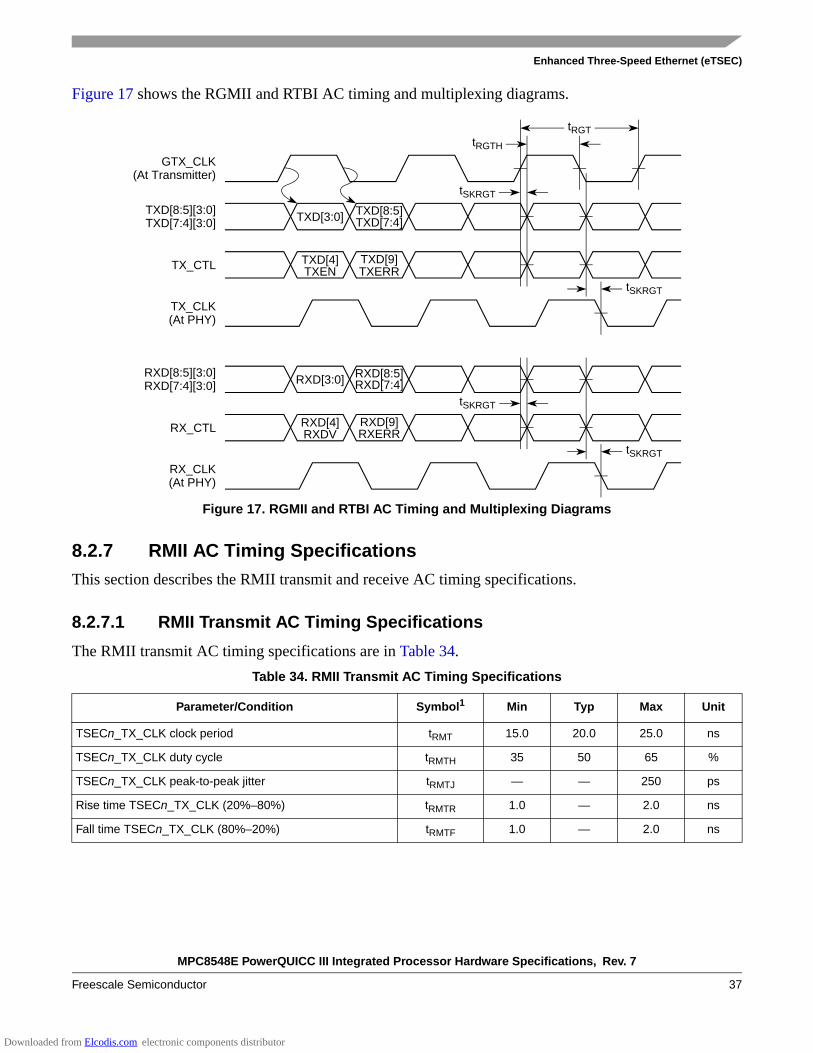
Figure 17 shows the RGMII and RTBI AC timing and multiplexing diagrams.
Figure 17. RGMII and RTBI AC Timing and Multiplexing Diagrams
8.2.7 RMII AC Timing SpecificationsThis section describes the RMII transmit and receive AC timing specifications.
8.2.7.1 RMII Transmit AC Timing Specifications
The RMII transmit AC timing specifications are in Table 34.Table 34. RMII Transmit AC Timing Specifications
Parameter/Condition Symbol1 Min Typ Max Unit
TSECn_TX_CLK clock period tRMT 15.0 20.0 25.0 ns
TSECn_TX_CLK duty cycle tRMTH 35 50 65 %
TSECn_TX_CLK peak-to-peak jitter tRMTJ — — 250 ps
Rise time TSECn_TX_CLK (20%–80%) tRMTR 1.0 — 2.0 ns
Fall time TSECn_TX_CLK (80%–20%) tRMTF 1.0 — 2.0 ns
GTX_CLK
tRGTtRGTH
tSKRGT
TX_CTL
TXD[8:5]TXD[7:4]
TXD[9]TXERR
TXD[4]TXEN
TXD[3:0]
(At Transmitter)
TXD[8:5][3:0]TXD[7:4][3:0]
TX_CLK(At PHY)
RX_CTL
RXD[8:5]RXD[7:4]
RXD[9]RXERR
RXD[4]RXDV
RXD[3:0]RXD[8:5][3:0]RXD[7:4][3:0]
RX_CLK(At PHY)
tSKRGT
tSKRGT
tSKRGT
Downloaded from Elcodis.com electronic components distributor

MPC8548E PowerQUICC III Integrated Processor Hardware Specifications, Rev. 7
38 Freescale Semiconductor
Enhanced Three-Speed Ethernet (eTSEC)
Figure 18 shows the RMII transmit AC timing diagram.
Figure 18. RMII Transmit AC Timing Diagram
8.2.7.2 RMII Receive AC Timing Specifications
TSECn_TX_CLK to RMII data TXD[1:0], TX_EN delay tRMTDX 1.0 — 10.0 ns
Note: 1. The symbols used for timing specifications follow the pattern of t(first two letters of functional block)(signal)(state)(reference)(state) for
inputs and t(first two letters of functional block)(reference)(state)(signal)(state) for outputs. For example, tMTKHDX symbolizes MII transmit timing (MT) for the time tMTX clock reference (K) going high (H) until data outputs (D) are invalid (X). Note that, in general, the clock reference symbol representation is based on two to three letters representing the clock of a particular functional. For example, the subscript of tMTX represents the MII(M) transmit (TX) clock. For rise and fall times, the latter convention is used with the appropriate letter: R (rise) or F (fall).
Table 35. RMII Receive AC Timing Specifications
Parameter/Condition Symbol1 Min Typ Max Unit
TSECn_TX_CLK clock period tRMR 15.0 20.0 25.0 ns
TSECn_TX_CLK duty cycle tRMRH 35 50 65 %
TSECn_TX_CLK peak-to-peak jitter tRMRJ — — 250 ps
Rise time TSECn_TX_CLK(20%–80%) tRMRR 1.0 — 2.0 ns
Fall time TSECn_TX_CLK (80%–20%) tRMRF 1.0 — 2.0 ns
RXD[1:0], CRS_DV, RX_ER setup time to REF_CLK rising edge tRMRDV 4.0 — — ns
RXD[1:0], CRS_DV, RX_ER hold time to REF_CLK rising edge tRMRDX 2.0 — — ns
Note: 1. The symbols used for timing specifications follow the pattern of t(first two letters of functional block)(signal)(state)(reference)(state) for
inputs and t(first two letters of functional block)(reference)(state)(signal)(state) for outputs. For example, tMRDVKH symbolizes MII receive timing (MR) with respect to the time data input signals (D) reach the valid state (V) relative to the tMRX clock reference (K) going to the high (H) state or setup time. Also, tMRDXKL symbolizes MII receive timing (GR) with respect to the time data input signals (D) went invalid (X) relative to the tMRX clock reference (K) going to the low (L) state or hold time. Note that, in general, the clock reference symbol representation is based on three letters representing the clock of a particular functional. For example, the subscript of tMRX represents the MII (M) receive (RX) clock. For rise and fall times, the latter convention is used with the appropriate letter: R (rise) or F (fall).
Table 34. RMII Transmit AC Timing Specifications (continued)
Parameter/Condition Symbol1 Min Typ Max Unit
TSECn_TX_CLK
TXD[1:0]
tRMTDX
tRMT
tRMTH
tRMTR
tRMTF
TX_ENTX_ER
Downloaded from Elcodis.com electronic components distributor

MPC8548E PowerQUICC III Integrated Processor Hardware Specifications, Rev. 7
Freescale Semiconductor 39
Ethernet Management Interface Electrical Characteristics
Figure 19 provides the AC test load for eTSEC.
Figure 19. eTSEC AC Test Load
Figure 20 shows the RMII receive AC timing diagram.
Figure 20. RMII Receive AC Timing Diagram
9 Ethernet Management Interface Electrical Characteristics
The electrical characteristics specified here apply to MII management interface signals MDIO (management data input/output) and MDC (management data clock). The electrical characteristics for GMII, RGMII, RMII, TBI, and RTBI are specified in “Section 8, “Enhanced Three-Speed Ethernet (eTSEC).”
9.1 MII Management DC Electrical CharacteristicsThe MDC and MDIO are defined to operate at a supply voltage of 3.3 V. The DC electrical characteristics for MDIO and MDC are provided in Table 36.
Table 36. MII Management DC Electrical Characteristics
Parameter Symbol Min Max Unit
Supply voltage (3.3 V) OVDD 3.13 3.47 V
Output high voltage (OVDD = Min, IOH = –1.0 mA) VOH 2.10 OVDD + 0.3 V
Output low voltage (OVDD = Min, IOL = 1.0 mA) VOL GND 0.50 V
Input high voltage VIH 2.0 — V
Input low voltage VIL — 0.90 V
Output Z0 = 50 Ω LVDD/2RL = 50 Ω
TSECn_TX_CLK
RXD[1:0]
tRMRDX
tRMR
tRMRH
tRMRR
tRMRF
CRS_DVRX_ER
tRMRDV
Valid Data
Downloaded from Elcodis.com electronic components distributor

MPC8548E PowerQUICC III Integrated Processor Hardware Specifications, Rev. 7
40 Freescale Semiconductor
Ethernet Management Interface Electrical Characteristics
9.2 MII Management AC Electrical SpecificationsTable 37 provides the MII management AC timing specifications.
Input high current (OVDD = Max, VIN1 = 2.1 V) IIH — 40 μA
Input low current (OVDD = Max, VIN = 0.5 V) IIL –600 — μA
Note:1. Note that the symbol VIN, in this case, represents the OVIN symbol referenced in Table 1 and Table 2.
Table 37. MII Management AC Timing SpecificationsAt recommended operating conditions with OVDD is 3.3 V ± 5%.
Parameter Symbol1 Min Typ Max Unit Notes
MDC frequency fMDC 0.72 2.5 8.3 MHz 2, 3, 4
MDC period tMDC 120.5 — 1389 ns —
MDC clock pulse width high tMDCH 32 — — ns —
MDC to MDIO valid tMDKHDV 16 × tCCB — — ns 5
MDC to MDIO delay tMDKHDX (16 × tCCB × 8) – 3 — (16 × tCCB × 8) + 3 ns 5
MDIO to MDC setup time tMDDVKH 5 — — ns —
MDIO to MDC hold time tMDDXKH 0 — — ns —
MDC rise time tMDCR — — 10 ns 4
MDC fall time tMDHF — 10 ns 4
Notes:1. The symbols used for timing specifications follow the pattern of t(first two letters of functional block)(signal)(state)(reference)(state) for
inputs and t(first two letters of functional block)(reference)(state)(signal)(state) for outputs. For example, tMDKHDX symbolizes management data timing (MD) for the time tMDC from clock reference (K) high (H) until data outputs (D) are invalid (X) or data hold time. Also, tMDDVKH symbolizes management data timing (MD) with respect to the time data input signals (D) reach the valid state (V) relative to the tMDC clock reference (K) going to the high (H) state or setup time. For rise and fall times, the latter convention is used with the appropriate letter: R (rise) or F (fall).
2. This parameter is dependent on the eTSEC system clock speed, which is half of the Platform Frequency (fCCB). The actual ECn_MDC output clock frequency for a specific eTSEC port can be programmed by configuring the MgmtClk bit field of MPC8548E’s MIIMCFG register, based on the platform (CCB) clock running for the device. The formula is: Platform Frequency (CCB) ÷ (2 × Frequency Divider determined by MIICFG[MgmtClk] encoding selection). For example, if MIICFG[MgmtClk] = 000 and the platform (CCB) is currently running at 533 MHz, fMDC = 533) ÷ (2 × 4 × 8) = 533) ÷ 64 = 8.3 MHz. That is, for a system running at a particular platform frequency (fCCB), the ECn_MDC output clock frequency can be programmed between maximum fMDC = fCCB ÷ 64 and minimum fMDC = fCCB ÷ 448. Refer to MPC8572E reference manual’s MIIMCFG register section for more detail.3.The maximum ECn_MDC output clock frequency is defined based on the maximum platform frequency for MPC8548E (533 MHz) divided by 64, while the minimum ECn_MDC output clock frequency is defined based on the minimum platform frequency for MPC8548E (333 MHz) divided by 448, following the formula described in Note 2 above.
4. Guaranteed by design.5. tCCB is the platform (CCB) clock period.
Table 36. MII Management DC Electrical Characteristics (continued)
Parameter Symbol Min Max Unit
Downloaded from Elcodis.com electronic components distributor
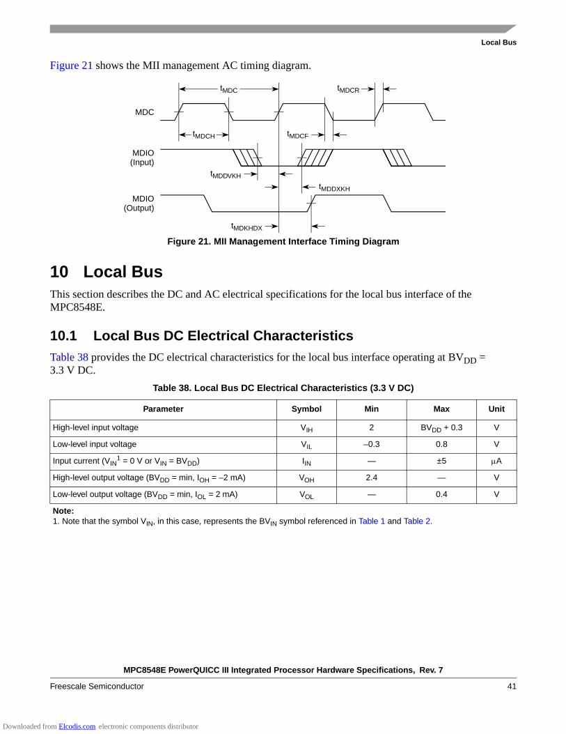
MPC8548E PowerQUICC III Integrated Processor Hardware Specifications, Rev. 7
Freescale Semiconductor 41
Local Bus
Figure 21 shows the MII management AC timing diagram.
Figure 21. MII Management Interface Timing Diagram
10 Local BusThis section describes the DC and AC electrical specifications for the local bus interface of the MPC8548E.
10.1 Local Bus DC Electrical CharacteristicsTable 38 provides the DC electrical characteristics for the local bus interface operating at BVDD = 3.3 V DC.
Table 38. Local Bus DC Electrical Characteristics (3.3 V DC)
Parameter Symbol Min Max Unit
High-level input voltage VIH 2 BVDD + 0.3 V
Low-level input voltage VIL –0.3 0.8 V
Input current (VIN1 = 0 V or VIN = BVDD) IIN — ±5 μA
High-level output voltage (BVDD = min, IOH = –2 mA) VOH 2.4 — V
Low-level output voltage (BVDD = min, IOL = 2 mA) VOL — 0.4 V
Note:1. Note that the symbol VIN, in this case, represents the BVIN symbol referenced in Table 1 and Table 2.
MDC
tMDDXKH
tMDC
tMDCH
tMDCR
tMDCF
tMDDVKH
tMDKHDX
MDIO
MDIO
(Input)
(Output)
Downloaded from Elcodis.com electronic components distributor

MPC8548E PowerQUICC III Integrated Processor Hardware Specifications, Rev. 7
42 Freescale Semiconductor
Local Bus
Table 39 provides the DC electrical characteristics for the local bus interface operating at BVDD = 2.5 V DC.
10.2 Local Bus AC Electrical SpecificationsTable 40 describes the timing parameters of the local bus interface at BVDD = 3.3 V. For information about the frequency range of local bus, see Section 19.1, “Clock Ranges.”
Table 39. Local Bus DC Electrical Characteristics (2.5 V DC)
Parameter Symbol Min Max Unit
High-level input voltage VIH 1.70 BVDD + 0.3 V
Low-level input voltage VIL –0.3 0.7 V
Input current (VIN1 = 0 V or VIN = BVDD) IIH — 10 μA
IIL –15
High-level output voltage (BVDD = min, IOH = –1 mA) VOH 2.0 — V
Low-level output voltage (BVDD = min, IOL = 1 mA) VOL — 0.4 V
Note:1. Note that the symbol VIN, in this case, represents the BVIN symbol referenced in Table 1 and Table 2.
Table 40. Local Bus Timing Parameters (BVDD = 3.3 V)—PLL Enabled
Parameter Symbol1 Min Max Unit Notes
Local bus cycle time tLBK 7.5 12 ns 2
Local bus duty cycle tLBKH/tLBK 43 57 % —
LCLK[n] skew to LCLK[m] or LSYNC_OUT tLBKSKEW — 150 ps 7, 8
Input setup to local bus clock (except LGTA/LUPWAIT) tLBIVKH1 1.8 — ns 3, 4
LGTA/LUPWAIT input setup to local bus clock tLBIVKH2 1.7 — ns 3, 4
Input hold from local bus clock (except LGTA/LUPWAIT) tLBIXKH1 1.0 — ns 3, 4
LGTA/LUPWAIT input hold from local bus clock tLBIXKH2 1.0 — ns 3, 4
LALE output transition to LAD/LDP output transition (LATCH hold time) tLBOTOT 1.5 — ns 6
Local bus clock to output valid (except LAD/LDP and LALE) tLBKHOV1 — 2.0 ns —
Local bus clock to data valid for LAD/LDP tLBKHOV2 — 2.2 ns 3
Local bus clock to address valid for LAD tLBKHOV3 — 2.3 ns 3
Local bus clock to LALE assertion tLBKHOV4 — 2.3 ns 3
Output hold from local bus clock (except LAD/LDP and LALE) tLBKHOX1 0.7 — ns 3
Output hold from local bus clock for LAD/LDP tLBKHOX2 0.7 — ns 3
Local bus clock to output high Impedance (except LAD/LDP and LALE) tLBKHOZ1 — 2.5 ns 5
Downloaded from Elcodis.com electronic components distributor

MPC8548E PowerQUICC III Integrated Processor Hardware Specifications, Rev. 7
Freescale Semiconductor 43
Local Bus
Table 41 describes the timing parameters of the local bus interface at BVDD = 2.5 V.
Local bus clock to output high impedance for LAD/LDP tLBKHOZ2 — 2.5 ns 5
Notes:1. The symbols used for timing specifications follow the pattern of t(first two letters of functional block)(signal)(state)(reference)(state) for
inputs and t(first two letters of functional block)(reference)(state)(signal)(state) for outputs. For example, tLBIXKH1 symbolizes local bus timing (LB) for the input (I) to go invalid (X) with respect to the time the tLBK clock reference (K) goes high (H), in this case for clock one (1). Also, tLBKHOX symbolizes local bus timing (LB) for the tLBK clock reference (K) to go high (H), with respect to the output (O) going invalid (X) or output hold time.
2. All timings are in reference to LSYNC_IN for PLL enabled and internal local bus clock for PLL bypass mode.3. All signals are measured from BVDD/2 of the rising edge of LSYNC_IN for PLL enabled or internal local bus clock for PLL
bypass mode to 0.4 × BVDD of the signal in question for 3.3-V signaling levels.4. Input timings are measured at the pin.5. For purposes of active/float timing measurements, the Hi-Z or off state is defined to be when the total current delivered
through the component pin is less than or equal to the leakage current specification.6. tLBOTOT is a measurement of the minimum time between the negation of LALE and any change in LAD. tLBOTOT is
programmed with the LBCR[AHD] parameter.7. Maximum possible clock skew between a clock LCLK[m] and a relative clock LCLK[n]. Skew measured between
complementary signals at BVDD/2.8. Guaranteed by design.
Table 41. Local Bus Timing Parameters (BVDD = 2.5 V)—PLL Enabled
Parameter Symbol1 Min Max Unit Notes
Local bus cycle time tLBK 7.5 12 ns 2
Local bus duty cycle tLBKH/tLBK 43 57 % —
LCLK[n] skew to LCLK[m] or LSYNC_OUT tLBKSKEW — 150 ps 7, 8
Input setup to local bus clock (except LGTA/UPWAIT) tLBIVKH1 1.9 — ns 3, 4
LGTA/LUPWAIT input setup to local bus clock tLBIVKH2 1.8 — ns 3, 4
Input hold from local bus clock (except LGTA/LUPWAIT) tLBIXKH1 1.1 — ns 3, 4
LGTA/LUPWAIT input hold from local bus clock tLBIXKH2 1.1 — ns 3, 4
LALE output transition to LAD/LDP output transition (LATCH hold time) tLBOTOT 1.5 — ns 6
Local bus clock to output valid (except LAD/LDP and LALE) tLBKHOV1 — 2.1 ns —
Local bus clock to data valid for LAD/LDP tLBKHOV2 — 2.3 ns 3
Local bus clock to address valid for LAD tLBKHOV3 — 2.4 ns 3
Local bus clock to LALE assertion tLBKHOV4 — 2.4 ns 3
Output hold from local bus clock (except LAD/LDP and LALE) tLBKHOX1 0.8 — ns 3
Output hold from local bus clock for LAD/LDP tLBKHOX2 0.8 — ns 3
Table 40. Local Bus Timing Parameters (BVDD = 3.3 V)—PLL Enabled (continued)
Parameter Symbol1 Min Max Unit Notes
Downloaded from Elcodis.com electronic components distributor
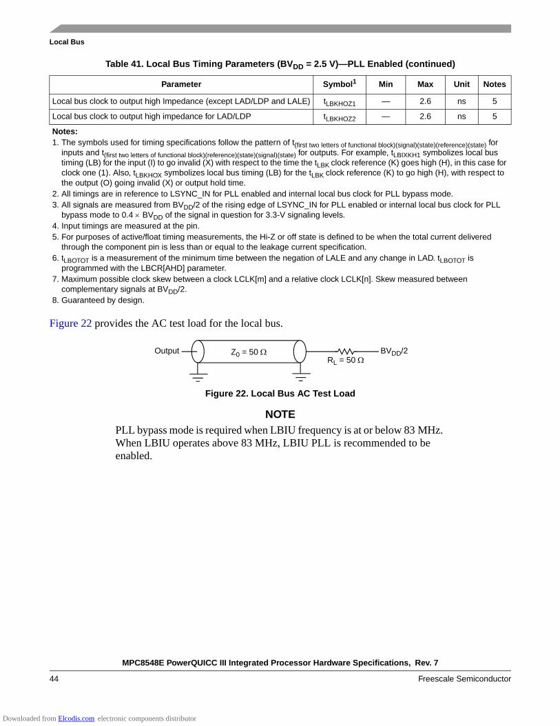
MPC8548E PowerQUICC III Integrated Processor Hardware Specifications, Rev. 7
44 Freescale Semiconductor
Local Bus
Figure 22 provides the AC test load for the local bus.
Figure 22. Local Bus AC Test Load
NOTEPLL bypass mode is required when LBIU frequency is at or below 83 MHz. When LBIU operates above 83 MHz, LBIU PLL is recommended to be enabled.
Local bus clock to output high Impedance (except LAD/LDP and LALE) tLBKHOZ1 — 2.6 ns 5
Local bus clock to output high impedance for LAD/LDP tLBKHOZ2 — 2.6 ns 5
Notes:1. The symbols used for timing specifications follow the pattern of t(first two letters of functional block)(signal)(state)(reference)(state) for
inputs and t(first two letters of functional block)(reference)(state)(signal)(state) for outputs. For example, tLBIXKH1 symbolizes local bus timing (LB) for the input (I) to go invalid (X) with respect to the time the tLBK clock reference (K) goes high (H), in this case for clock one (1). Also, tLBKHOX symbolizes local bus timing (LB) for the tLBK clock reference (K) to go high (H), with respect to the output (O) going invalid (X) or output hold time.
2. All timings are in reference to LSYNC_IN for PLL enabled and internal local bus clock for PLL bypass mode.3. All signals are measured from BVDD/2 of the rising edge of LSYNC_IN for PLL enabled or internal local bus clock for PLL
bypass mode to 0.4 × BVDD of the signal in question for 3.3-V signaling levels.4. Input timings are measured at the pin.5. For purposes of active/float timing measurements, the Hi-Z or off state is defined to be when the total current delivered
through the component pin is less than or equal to the leakage current specification.6. tLBOTOT is a measurement of the minimum time between the negation of LALE and any change in LAD. tLBOTOT is
programmed with the LBCR[AHD] parameter.7. Maximum possible clock skew between a clock LCLK[m] and a relative clock LCLK[n]. Skew measured between
complementary signals at BVDD/2.8. Guaranteed by design.
Table 41. Local Bus Timing Parameters (BVDD = 2.5 V)—PLL Enabled (continued)
Parameter Symbol1 Min Max Unit Notes
Output Z0 = 50 Ω BVDD/2RL = 50 Ω
Downloaded from Elcodis.com electronic components distributor
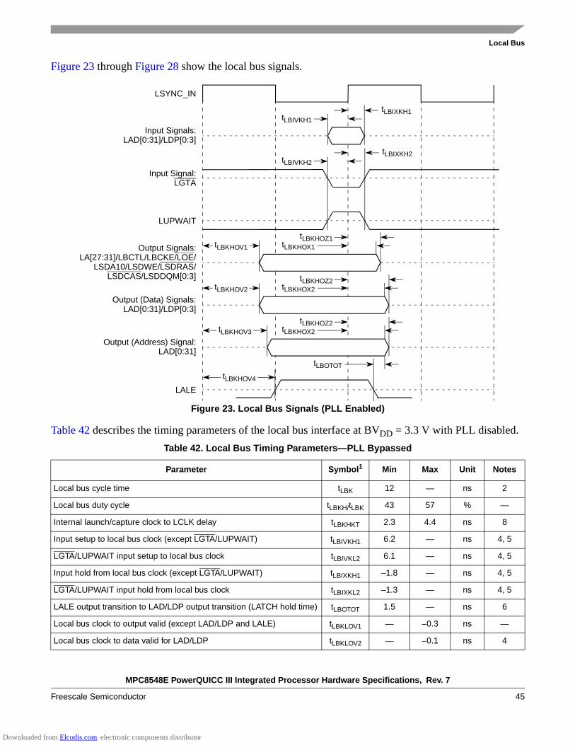
MPC8548E PowerQUICC III Integrated Processor Hardware Specifications, Rev. 7
Freescale Semiconductor 45
Local Bus
Figure 23 through Figure 28 show the local bus signals.
Figure 23. Local Bus Signals (PLL Enabled)
Table 42 describes the timing parameters of the local bus interface at BVDD = 3.3 V with PLL disabled.Table 42. Local Bus Timing Parameters—PLL Bypassed
Parameter Symbol1 Min Max Unit Notes
Local bus cycle time tLBK 12 — ns 2
Local bus duty cycle tLBKH/tLBK 43 57 % —
Internal launch/capture clock to LCLK delay tLBKHKT 2.3 4.4 ns 8
Input setup to local bus clock (except LGTA/LUPWAIT) tLBIVKH1 6.2 — ns 4, 5
LGTA/LUPWAIT input setup to local bus clock tLBIVKL2 6.1 — ns 4, 5
Input hold from local bus clock (except LGTA/LUPWAIT) tLBIXKH1 –1.8 — ns 4, 5
LGTA/LUPWAIT input hold from local bus clock tLBIXKL2 –1.3 — ns 4, 5
LALE output transition to LAD/LDP output transition (LATCH hold time) tLBOTOT 1.5 — ns 6
Local bus clock to output valid (except LAD/LDP and LALE) tLBKLOV1 — –0.3 ns —
Local bus clock to data valid for LAD/LDP tLBKLOV2 — –0.1 ns 4
Output Signals:LA[27:31]/LBCTL/LBCKE/LOE/
LSDA10/LSDWE/LSDRAS/LSDCAS/LSDDQM[0:3]
tLBKHOV1
tLBKHOV2
tLBKHOV3
LSYNC_IN
Input Signals:LAD[0:31]/LDP[0:3]
Output (Data) Signals:LAD[0:31]/LDP[0:3]
Output (Address) Signal:LAD[0:31]
LALE
tLBIXKH1tLBIVKH1
tLBIVKH2
tLBIXKH2
tLBKHOX1
tLBKHOZ1
tLBKHOX2
tLBKHOZ2
Input Signal:LGTA
tLBOTOT
tLBKHOZ2tLBKHOX2
tLBKHOV4
LUPWAIT
Downloaded from Elcodis.com electronic components distributor
MPC8548E PowerQUICC III Integrated Processor Hardware Specifications, Rev. 7
46 Freescale Semiconductor
Local Bus
Local bus clock to address valid for LAD tLBKLOV3 — 0 ns 4
Local bus clock to LALE assertion tLBKLOV4 — 0 ns 4
Output hold from local bus clock (except LAD/LDP and LALE) tLBKLOX1 –3.7 — ns 4
Output hold from local bus clock for LAD/LDP tLBKLOX2 –3.7 — ns 4
Local bus clock to output high Impedance (except LAD/LDP and LALE) tLBKLOZ1 — 0.2 ns 7
Local bus clock to output high impedance for LAD/LDP tLBKLOZ2 — 0.2 ns 7
Notes:1. The symbols used for timing specifications follow the pattern of t(first two letters of functional block)(signal)(state)(reference)(state) for
inputs and t(first two letters of functional block)(reference)(state)(signal)(state) for outputs. For example, tLBIXKH1 symbolizes local bus timing (LB) for the input (I) to go invalid (X) with respect to the time the tLBK clock reference (K) goes high (H), in this case for clock one (1). Also, tLBKHOX symbolizes local bus timing (LB) for the tLBK clock reference (K) to go high (H), with respect to the output (O) going invalid (X) or output hold time.
2. All timings are in reference to local bus clock for PLL bypass mode. Timings may be negative with respect to the local bus clock because the actual launch and capture of signals is done with the internal launch/capture clock, which precedes LCLK by tLBKHKT.
3. Maximum possible clock skew between a clock LCLK[m] and a relative clock LCLK[n]. Skew measured between complementary signals at BVDD/2.
4. All signals are measured from BVDD/2 of the rising edge of local bus clock for PLL bypass mode to 0.4 × BVDD of the signal in question for 3.3-V signaling levels.
5. Input timings are measured at the pin.6. The value of tLBOTOT is the measurement of the minimum time between the negation of LALE and any change in LAD.7. For purposes of active/float timing measurements, the Hi-Z or off state is defined to be when the total current delivered
through the component pin is less than or equal to the leakage current specification.8. Guaranteed by characterization.9. Guaranteed by design.
Table 42. Local Bus Timing Parameters—PLL Bypassed (continued)
Parameter Symbol1 Min Max Unit Notes
Downloaded from Elcodis.com electronic components distributor
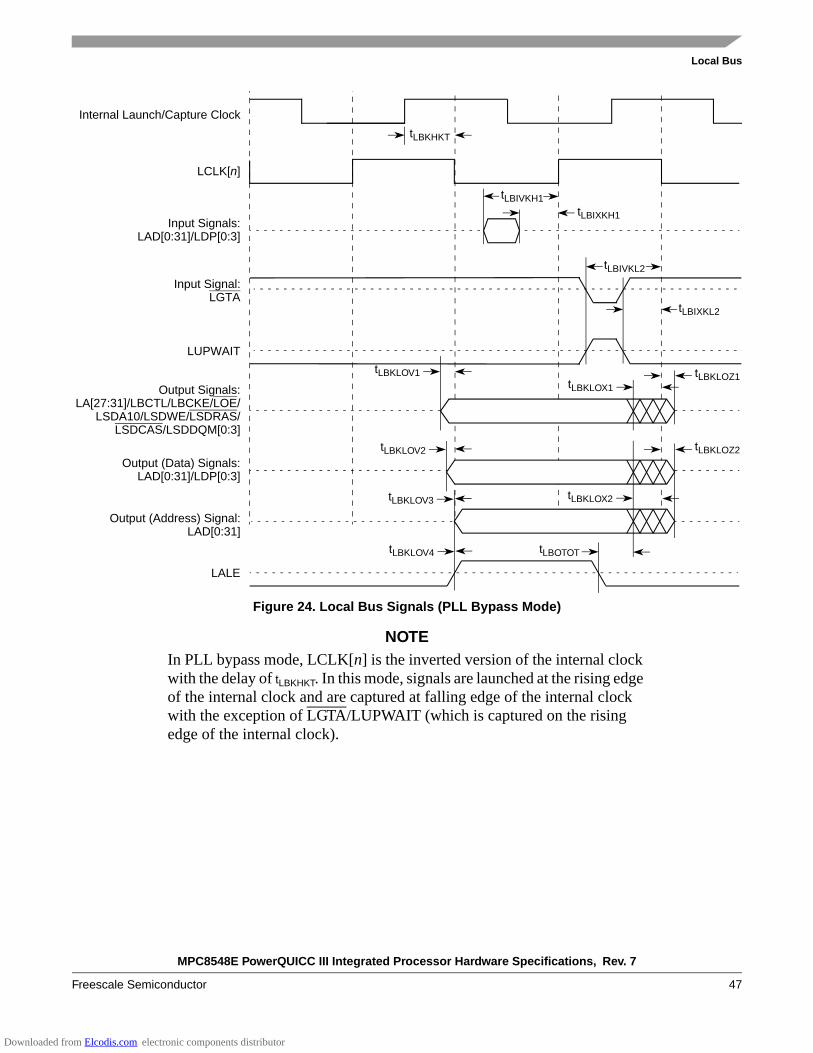
MPC8548E PowerQUICC III Integrated Processor Hardware Specifications, Rev. 7
Freescale Semiconductor 47
Local Bus
Figure 24. Local Bus Signals (PLL Bypass Mode)
NOTEIn PLL bypass mode, LCLK[n] is the inverted version of the internal clock with the delay of tLBKHKT. In this mode, signals are launched at the rising edge of the internal clock and are captured at falling edge of the internal clock with the exception of LGTA/LUPWAIT (which is captured on the rising edge of the internal clock).
Output Signals:LA[27:31]/LBCTL/LBCKE/LOE/
LSDA10/LSDWE/LSDRAS/LSDCAS/LSDDQM[0:3]
tLBKLOV2
LCLK[n]
Input Signals:LAD[0:31]/LDP[0:3]
Output (Data) Signals:LAD[0:31]/LDP[0:3]
LALE
tLBIXKH1
Input Signal:LGTA
Output (Address) Signal:LAD[0:31]
tLBIVKH1
tLBIXKL2
tLBIVKL2
tLBKLOX1
tLBKLOZ2
tLBOTOT
Internal Launch/Capture Clock
tLBKLOX2
tLBKLOV1
tLBKLOV3
tLBKLOZ1
tLBKHKT
tLBKLOV4
LUPWAIT
Downloaded from Elcodis.com electronic components distributor

MPC8548E PowerQUICC III Integrated Processor Hardware Specifications, Rev. 7
48 Freescale Semiconductor
Local Bus
Figure 25. Local Bus Signals, GPCM/UPM Signals for LCCR[CLKDIV] = 4 (PLL Enabled)
LSYNC_IN
UPM Mode Input Signal:LUPWAIT
tLBIXKH2
tLBIVKH2
tLBIVKH1
tLBIXKH1
tLBKHOZ1
T1
T3
Input Signals:LAD[0:31]/LDP[0:3]
UPM Mode Output Signals:LCS[0:7]/LBS[0:3]/LGPL[0:5]
GPCM Mode Output Signals:LCS[0:7]/LWE
tLBKHOV1
tLBKHOV1 tLBKHOZ1
GPCM Mode Input Signal:LGTA
Downloaded from Elcodis.com electronic components distributor
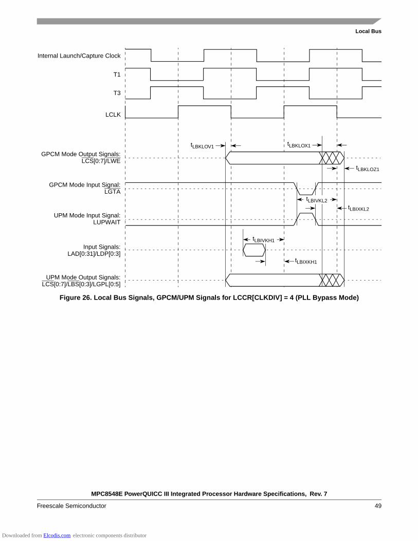
MPC8548E PowerQUICC III Integrated Processor Hardware Specifications, Rev. 7
Freescale Semiconductor 49
Local Bus
Figure 26. Local Bus Signals, GPCM/UPM Signals for LCCR[CLKDIV] = 4 (PLL Bypass Mode)
tLBIVKH1
tLBIXKL2
Internal Launch/Capture Clock
UPM Mode Input Signal:LUPWAIT
T1
T3
Input Signals:LAD[0:31]/LDP[0:3]
UPM Mode Output Signals:LCS[0:7]/LBS[0:3]/LGPL[0:5]
GPCM Mode Output Signals:LCS[0:7]/LWE
tLBKLOV1
tLBKLOZ1
LCLK
tLBKLOX1
tLBIXKH1
GPCM Mode Input Signal:LGTA
tLBIVKL2
Downloaded from Elcodis.com electronic components distributor

MPC8548E PowerQUICC III Integrated Processor Hardware Specifications, Rev. 7
50 Freescale Semiconductor
Local Bus
Figure 27. Local Bus Signals, GPCM/UPM Signals for LCCR[CLKDIV] = 8 or 16 (PLL Enabled)
LSYNC_IN
UPM Mode Input Signal:LUPWAIT
tLBIXKH2
tLBIVKH2
tLBIVKH1
tLBIXKH1
tLBKHOZ1
T1
T3
UPM Mode Output Signals:LCS[0:7]/LBS[0:3]/LGPL[0:5]
GPCM Mode Output Signals:LCS[0:7]/LWE
tLBKHOV1
tLBKHOV1 tLBKHOZ1
T2
T4
Input Signals:LAD[0:31]/LDP[0:3]
GPCM Mode Input Signal:LGTA
Downloaded from Elcodis.com electronic components distributor

MPC8548E PowerQUICC III Integrated Processor Hardware Specifications, Rev. 7
Freescale Semiconductor 51
Programmable Interrupt Controller
Figure 28. Local Bus Signals, GPCM/UPM Signals for LCCR[CLKDIV] = 8 or 16 (PLL Bypass Mode)
11 Programmable Interrupt ControllerIn IRQ edge trigger mode, when an external interrupt signal is asserted (according to the programmed polarity), it must remain the assertion for at least 3 system clocks (SYSCLK periods).
12 JTAGThis section describes the DC and AC electrical specifications for the IEEE 1149.1 (JTAG) interface of the MPC8548E.
tLBIXKL2
tLBIVKH1
Internal Launch/Capture Clock
UPM Mode Input Signal:LUPWAIT
T1
T3
UPM Mode Output Signals:LCS[0:7]/LBS[0:3]/LGPL[0:5]
GPCM Mode Output Signals:LCS[0:7]/LWE
T2
T4
Input Signals:LAD[0:31]/LDP[0:3]
LCLK
tLBKLOV1
tLBKLOZ1
tLBKLOX1
tLBIXKH1
GPCM Mode Input Signal:LGTA
tLBIVKL2
Downloaded from Elcodis.com electronic components distributor

MPC8548E PowerQUICC III Integrated Processor Hardware Specifications, Rev. 7
52 Freescale Semiconductor
JTAG
12.1 JTAG DC Electrical CharacteristicsTable 43 provides the DC electrical characteristics for the JTAG interface.
12.2 JTAG AC Electrical SpecificationsTable 44 provides the JTAG AC timing specifications as defined in Figure 30 through Figure 32.
Table 43. JTAG DC Electrical Characteristics
Parameter Symbol1 Min Max Unit
High-level input voltage VIH 2 OVDD + 0.3 V
Low-level input voltage VIL –0.3 0.8 V
Input current (VIN1 = 0 V or VIN = VDD) IIN — ±5 μA
High-level output voltage (OVDD = min, IOH = –2 mA) VOH 2.4 — V
Low-level output voltage (OVDD = min, IOL = 2 mA) VOL — 0.4 V
Note:1. Note that the symbol VIN, in this case, represents the OVIN.
Table 44. JTAG AC Timing Specifications (Independent of SYSCLK)1
Parameter Symbol2 Min Max Unit Notes
JTAG external clock frequency of operation fJTG 0 33.3 MHz —
JTAG external clock cycle time t JTG 30 — ns —
JTAG external clock pulse width measured at 1.4 V tJTKHKL 15 — ns —
JTAG external clock rise and fall times tJTGR & tJTGF 0 2 ns 6
TRST assert time tTRST 25 — ns 3
Input setup times:Boundary-scan data
TMS, TDItJTDVKHtJTIVKH
40
——
ns4
Input hold times:Boundary-scan data
TMS, TDItJTDXKHtJTIXKH
2025
——
ns4
Valid times:Boundary-scan data
TDOtJTKLDVtJTKLOV
44
2025
ns5
Output hold times:Boundary-scan data
TDOtJTKLDXtJTKLOX
3030
——
ns5
Downloaded from Elcodis.com electronic components distributor

MPC8548E PowerQUICC III Integrated Processor Hardware Specifications, Rev. 7
Freescale Semiconductor 53
JTAG
Figure 29 provides the AC test load for TDO and the boundary-scan outputs.
Figure 29. AC Test Load for the JTAG Interface
Figure 30 provides the JTAG clock input timing diagram.
Figure 30. JTAG Clock Input Timing Diagram
Figure 31 provides the TRST timing diagram.
Figure 31. TRST Timing Diagram
JTAG external clock to output high impedance:Boundary-scan data
TDOtJTKLDZtJTKLOZ
33
199
ns5, 6
Notes:1. All outputs are measured from the midpoint voltage of the falling/rising edge of tTCLK to the midpoint of the signal in question.
The output timings are measured at the pins. All output timings assume a purely resistive 50-Ω load (see Figure 29). Time-of-flight delays must be added for trace lengths, vias, and connectors in the system.
2. The symbols used for timing specifications follow the pattern of t(first two letters of functional block)(signal)(state)(reference)(state) for inputs and t(first two letters of functional block)(reference)(state)(signal)(state) for outputs. For example, tJTDVKH symbolizes JTAG device timing (JT) with respect to the time data input signals (D) reaching the valid state (V) relative to the tJTG clock reference (K) going to the high (H) state or setup time. Also, tJTDXKH symbolizes JTAG timing (JT) with respect to the time data input signals (D) went invalid (X) relative to the tJTG clock reference (K) going to the high (H) state. Note that, in general, the clock reference symbol representation is based on three letters representing the clock of a particular functional. For rise and fall times, the latter convention is used with the appropriate letter: R (rise) or F (fall).
3. TRST is an asynchronous level sensitive signal. The setup time is for test purposes only.4. Non-JTAG signal input timing with respect to tTCLK.5. Non-JTAG signal output timing with respect to tTCLK.6. Guaranteed by design.
Table 44. JTAG AC Timing Specifications (Independent of SYSCLK)1 (continued)
Parameter Symbol2 Min Max Unit Notes
Output Z0 = 50 Ω OVDD/2RL = 50 Ω
JTAG
tJTKHKL tJTGR
External Clock VMVMVM
tJTG tJTGF
VM = Midpoint Voltage (OVDD/2)
TRST
VM = Midpoint Voltage (OVDD/2)
VM VM
tTRST
Downloaded from Elcodis.com electronic components distributor
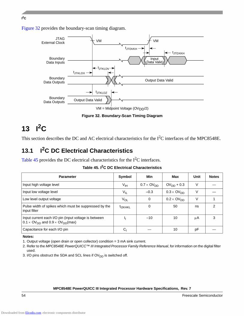
MPC8548E PowerQUICC III Integrated Processor Hardware Specifications, Rev. 7
54 Freescale Semiconductor
I2C
Figure 32 provides the boundary-scan timing diagram.
Figure 32. Boundary-Scan Timing Diagram
13 I2C This section describes the DC and AC electrical characteristics for the I2C interfaces of the MPC8548E.
13.1 I2C DC Electrical CharacteristicsTable 45 provides the DC electrical characteristics for the I2C interfaces.
Table 45. I2C DC Electrical Characteristics
Parameter Symbol Min Max Unit Notes
Input high voltage level VIH 0.7 × OVDD OVDD + 0.3 V —
Input low voltage level VIL –0.3 0.3 × OVDD V —
Low level output voltage VOL 0 0.2 × OVDD V 1
Pulse width of spikes which must be suppressed by the input filter
tI2KHKL 0 50 ns 2
Input current each I/O pin (input voltage is between 0.1 × OVDD and 0.9 × OVDD(max)
II –10 10 μA 3
Capacitance for each I/O pin CI — 10 pF —
Notes:1. Output voltage (open drain or open collector) condition = 3 mA sink current.2. Refer to the MPC8548E PowerQUICC™ III Integrated Processor Family Reference Manual, for information on the digital filter
used.3. I/O pins obstruct the SDA and SCL lines if OVDD is switched off.
VM = Midpoint Voltage (OVDD/2)
VM VM
tJTDVKHtJTDXKH
BoundaryData Outputs
BoundaryData Outputs
JTAGExternal Clock
BoundaryData Inputs
Output Data Valid
tJTKLDX
tJTKLDZ
tJTKLDV
InputData Valid
Output Data Valid
Downloaded from Elcodis.com electronic components distributor

MPC8548E PowerQUICC III Integrated Processor Hardware Specifications, Rev. 7
Freescale Semiconductor 55
I2C
13.2 I2C AC Electrical SpecificationsTable 46 provides the AC timing parameters for the I2C interfaces.
Table 46. I2C AC Electrical Specifications
Parameter Symbol1 Min Max Unit Notes
SCL clock frequency fI2C 0 400 kHz —
Low period of the SCL clock tI2CL 1.3 — μs 4
High period of the SCL clock tI2CH 0.6 — μs 4
Setup time for a repeated START condition tI2SVKH 0.6 — μs 4
Hold time (repeated) START condition (after this period, the first clock pulse is generated)
tI2SXKL 0.6 — μs 4
Data setup time tI2DVKH 100 — ns 4
Data input hold time:CBUS compatible masters
I2C bus devices
tI2DXKL—0
——
μs 2
Data output delay time: tI2OVKL — 0.9 — 3
Set-up time for STOP condition tI2PVKH 0.6 — μs —
Bus free time between a STOP and START condition tI2KHDX 1.3 — μs —
Noise margin at the LOW level for each connected device (including hysteresis)
VNL 0.1 × OVDD — V —
Noise margin at the HIGH level for each connected device (including hysteresis)
VNH 0.2 × OVDD — V —
Notes:1. The symbols used for timing specifications follow the pattern of t(first two letters of functional block)(signal)(state)(reference)(state) for
inputs and t(first two letters of functional block)(reference)(state)(signal)(state) for outputs. For example, tI2DVKH symbolizes I2C timing (I2) with respect to the time data input signals (D) reach the valid state (V) relative to the tI2C clock reference (K) going to the high (H) state or setup time. Also, tI2SXKL symbolizes I2C timing (I2) for the time that the data with respect to the start condition (S) went invalid (X) relative to the tI2C clock reference (K) going to the low (L) state or hold time. Also, tI2PVKH symbolizes I2C timing (I2) for the time that the data with respect to the stop condition (P) reaching the valid state (V) relative to the tI2C clock reference (K) going to the high (H) state or setup time. For rise and fall times, the latter convention is used with the appropriate letter: R (rise) or F (fall).
2. As a transmitter, the MPC8548E provides a delay time of at least 300 ns for the SDA signal (refer to the VIH(min) of the SCL signal) to bridge the undefined region of the falling edge of SCL to avoid unintended generation of Start or Stop condition. When MPC8548E acts as the I2C bus master while transmitting, MPC8548E drives both SCL and SDA. As long as the load on SCL and SDA are balanced, MPC8548E would not cause unintended generation of Start or Stop condition. Therefore, the 300 ns SDA output delay time is not a concern. If, under some rare condition, the 300 ns SDA output delay time is required for MPC8548E as transmitter, the following setting is recommended for the FDR bit field of the I2CFDR register to ensure both the desired I2C SCL clock frequency and SDA output delay time are achieved, assuming that the desired I2C SCL clock frequency is 400 kHz and the Digital Filter Sampling Rate Register (I2CDFSRR) is programmed with its default setting of 0x10 (decimal 16):I2C source clock frequency 333 MHz 266 MHz 200 MHz 133 MHz
FDR bit setting 0x2A 0x05 0x26 0x00 Actual FDR divider selected 896 704 512 384 Actual I2C SCL frequency generated 371 kHz 378 kHz 390 kHz 346 kHz
For the detail of I2C frequency calculation, refer to Freescale Application Note AN2919, Determining the I2C Frequency Divider Ratio for SCL. Note that the I2C source clock frequency is half of the CCB clock frequency for MPC8548E.
3. The maximum tI2DXKL has only to be met if the device does not stretch the LOW period (tI2CL) of the SCL signal.4. Guaranteed by design.
Downloaded from Elcodis.com electronic components distributor
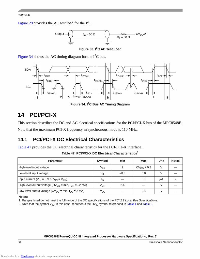
MPC8548E PowerQUICC III Integrated Processor Hardware Specifications, Rev. 7
56 Freescale Semiconductor
PCI/PCI-X
Figure 29 provides the AC test load for the I2C.
Figure 33. I2C AC Test Load
Figure 34 shows the AC timing diagram for the I2C bus.
Figure 34. I2C Bus AC Timing Diagram
14 PCI/PCI-XThis section describes the DC and AC electrical specifications for the PCI/PCI-X bus of the MPC8548E.
Note that the maximum PCI-X frequency in synchronous mode is 110 MHz.
14.1 PCI/PCI-X DC Electrical CharacteristicsTable 47 provides the DC electrical characteristics for the PCI/PCI-X interface.
Table 47. PCI/PCI-X DC Electrical Characteristics1
Parameter Symbol Min Max Unit Notes
High-level input voltage VIH 2 OVDD + 0.3 V —
Low-level input voltage VIL –0.3 0.8 V —
Input current (VIN = 0 V or VIN = VDD) IIN — ±5 μA 2
High-level output voltage (OVDD = min, IOH = –2 mA) VOH 2.4 — V —
Low-level output voltage (OVDD = min, IOL = 2 mA) VOL — 0.4 V —
Notes:1. Ranges listed do not meet the full range of the DC specifications of the PCI 2.2 Local Bus Specifications.2. Note that the symbol VIN, in this case, represents the OVIN symbol referenced in Table 1 and Table 2.
Output Z0 = 50 Ω OVDD/2RL = 50 Ω
SrS
SDA
SCL
tI2CF
tI2SXKL
tI2CL
tI2CHtI2DXKL,tI2OVKL
tI2DVKH
tI2SXKL
tI2SVKH
tI2KHKL
tI2PVKH
tI2CR
tI2CF
P S
Downloaded from Elcodis.com electronic components distributor
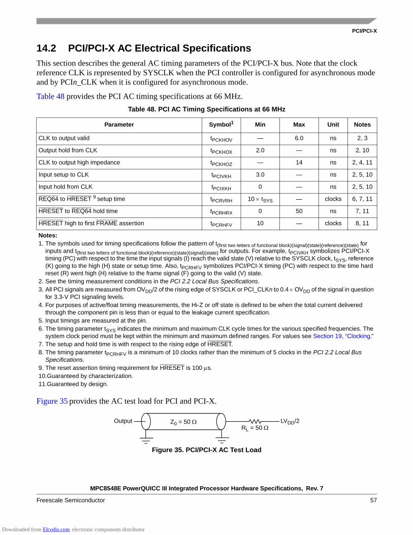
MPC8548E PowerQUICC III Integrated Processor Hardware Specifications, Rev. 7
Freescale Semiconductor 57
PCI/PCI-X
14.2 PCI/PCI-X AC Electrical SpecificationsThis section describes the general AC timing parameters of the PCI/PCI-X bus. Note that the clock reference CLK is represented by SYSCLK when the PCI controller is configured for asynchronous mode and by PCIn_CLK when it is configured for asynchronous mode.
Table 48 provides the PCI AC timing specifications at 66 MHz.
Figure 35 provides the AC test load for PCI and PCI-X.
Figure 35. PCI/PCI-X AC Test Load
Table 48. PCI AC Timing Specifications at 66 MHz
Parameter Symbol1 Min Max Unit Notes
CLK to output valid tPCKHOV — 6.0 ns 2, 3
Output hold from CLK tPCKHOX 2.0 — ns 2, 10
CLK to output high impedance tPCKHOZ — 14 ns 2, 4, 11
Input setup to CLK tPCIVKH 3.0 — ns 2, 5, 10
Input hold from CLK tPCIXKH 0 — ns 2, 5, 10
REQ64 to HRESET 9 setup time tPCRVRH 10 × tSYS — clocks 6, 7, 11
HRESET to REQ64 hold time tPCRHRX 0 50 ns 7, 11
HRESET high to first FRAME assertion tPCRHFV 10 — clocks 8, 11
Notes:1. The symbols used for timing specifications follow the pattern of t(first two letters of functional block)(signal)(state)(reference)(state) for
inputs and t(first two letters of functional block)(reference)(state)(signal)(state) for outputs. For example, tPCIVKH symbolizes PCI/PCI-X timing (PC) with respect to the time the input signals (I) reach the valid state (V) relative to the SYSCLK clock, tSYS, reference (K) going to the high (H) state or setup time. Also, tPCRHFV symbolizes PCI/PCI-X timing (PC) with respect to the time hard reset (R) went high (H) relative to the frame signal (F) going to the valid (V) state.
2. See the timing measurement conditions in the PCI 2.2 Local Bus Specifications.3. All PCI signals are measured from OVDD/2 of the rising edge of SYSCLK or PCI_CLKn to 0.4 × OVDD of the signal in question
for 3.3-V PCI signaling levels.4. For purposes of active/float timing measurements, the Hi-Z or off state is defined to be when the total current delivered
through the component pin is less than or equal to the leakage current specification.5. Input timings are measured at the pin.6. The timing parameter tSYS indicates the minimum and maximum CLK cycle times for the various specified frequencies. The
system clock period must be kept within the minimum and maximum defined ranges. For values see Section 19, “Clocking.” 7. The setup and hold time is with respect to the rising edge of HRESET.8. The timing parameter tPCRHFV is a minimum of 10 clocks rather than the minimum of 5 clocks in the PCI 2.2 Local Bus
Specifications.9. The reset assertion timing requirement for HRESET is 100 μs.10.Guaranteed by characterization.11.Guaranteed by design.
Output Z0 = 50 Ω LVDD/2RL = 50 Ω
Downloaded from Elcodis.com electronic components distributor
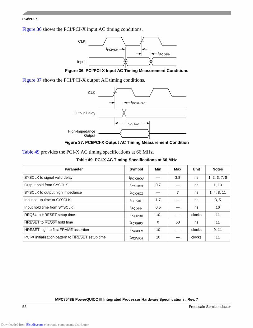
MPC8548E PowerQUICC III Integrated Processor Hardware Specifications, Rev. 7
58 Freescale Semiconductor
PCI/PCI-X
Figure 36 shows the PCI/PCI-X input AC timing conditions.
Figure 36. PCI/PCI-X Input AC Timing Measurement Conditions
Figure 37 shows the PCI/PCI-X output AC timing conditions.
Figure 37. PCI/PCI-X Output AC Timing Measurement Condition
Table 49 provides the PCI-X AC timing specifications at 66 MHz.Table 49. PCI-X AC Timing Specifications at 66 MHz
Parameter Symbol Min Max Unit Notes
SYSCLK to signal valid delay tPCKHOV — 3.8 ns 1, 2, 3, 7, 8
Output hold from SYSCLK tPCKHOX 0.7 — ns 1, 10
SYSCLK to output high impedance tPCKHOZ — 7 ns 1, 4, 8, 11
Input setup time to SYSCLK tPCIVKH 1.7 — ns 3, 5
Input hold time from SYSCLK tPCIXKH 0.5 — ns 10
REQ64 to HRESET setup time tPCRVRH 10 — clocks 11
HRESET to REQ64 hold time tPCRHRX 0 50 ns 11
HRESET high to first FRAME assertion tPCRHFV 10 — clocks 9, 11
PCI-X initialization pattern to HRESET setup time tPCIVRH 10 — clocks 11
tPCIVKH
CLK
Input
tPCIXKH
CLK
Output Delay
tPCKHOV
High-Impedance
tPCKHOZ
Output
Downloaded from Elcodis.com electronic components distributor
MPC8548E PowerQUICC III Integrated Processor Hardware Specifications, Rev. 7
Freescale Semiconductor 59
PCI/PCI-X
Table 50 provides the PCI-X AC timing specifications at 133 MHz. Note that the maximum PCI-X frequency in synchronous mode is 110 MHz.
HRESET to PCI-X initialization pattern hold time tPCRHIX 0 50 ns 6, 11
Notes:1. See the timing measurement conditions in the PCI-X 1.0a Specification.2. Minimum times are measured at the package pin (not the test point). Maximum times are measured with the test point and
load circuit.3. Setup time for point-to-point signals applies to REQ and GNT only. All other signals are bused.4. For purposes of active/float timing measurements, the Hi-Z or off state is defined to be when the total current delivered
through the component pin is less than or equal to the leakage current specification.5. Setup time applies only when the device is not driving the pin. Devices cannot drive and receive signals at the same time.6. Maximum value is also limited by delay to the first transaction (time for HRESET high to first configuration access, tPCRHFV).
The PCI-X initialization pattern control signals after the rising edge of HRESET must be negated no later than two clocks before the first FRAME and must be floated no later than one clock before FRAME is asserted.
7. A PCI-X device is permitted to have the minimum values shown for tPCKHOV and tCYC only in PCI-X mode. In conventional mode, the device must meet the requirements specified in PCI 2.2 for the appropriate clock frequency.
8. Device must meet this specification independent of how many outputs switch simultaneously.9. The timing parameter tPCRHFV is a minimum of 10 clocks rather than the minimum of 5 clocks in the PCI-X 1.0a Specification.10.Guaranteed by characterization.11.Guaranteed by design.
Table 50. PCI-X AC Timing Specifications at 133 MHz
Parameter Symbol Min Max Unit Notes
SYSCLK to signal valid delay tPCKHOV — 3.8 ns 1, 2, 3, 7, 8
Output hold from SYSCLK tPCKHOX 0.7 — ns 1, 11
SYSCLK to output high impedance tPCKHOZ — 7 ns 1, 4, 8, 12
Input setup time to SYSCLK tPCIVKH 1.2 — ns 3, 5, 9, 11
Input hold time from SYSCLK tPCIXKH 0.5 — ns 11
REQ64 to HRESET setup time tPCRVRH 10 — clocks 12
HRESET to REQ64 hold time tPCRHRX 0 50 ns 12
HRESET high to first FRAME assertion tPCRHFV 10 — clocks 10, 12
PCI-X initialization pattern to HRESET setup time tPCIVRH 10 — clocks 12
Table 49. PCI-X AC Timing Specifications at 66 MHz (continued)
Parameter Symbol Min Max Unit Notes
Downloaded from Elcodis.com electronic components distributor

MPC8548E PowerQUICC III Integrated Processor Hardware Specifications, Rev. 7
60 Freescale Semiconductor
High-Speed Serial Interfaces (HSSI)
15 High-Speed Serial Interfaces (HSSI)The MPC8548E features one Serializer/Deserializer (SerDes) interface to be used for high-speed serial interconnect applications. The SerDes interface can be used for PCI Express and/or serial RapidIO data transfers.
This section describes the common portion of SerDes DC electrical specifications, which is the DC requirement for SerDes reference clocks. The SerDes data lane’s transmitter and receiver reference circuits are also shown.
15.1 Signal Terms DefinitionThe SerDes utilizes differential signaling to transfer data across the serial link. This section defines terms used in the description and specification of differential signals.
Figure 38 shows how the signals are defined. For illustration purpose, only one SerDes lane is used for the description. The figure shows a waveform for either a transmitter output (SD_TX and SD_TX) or a receiver input (SD_RX and SD_RX). Each signal swings between A volts and B volts where A > B.
HRESET to PCI-X initialization pattern hold time tPCRHIX 0 50 ns 6, 12
Notes:1. See the timing measurement conditions in the PCI-X 1.0a Specification.2. Minimum times are measured at the package pin (not the test point). Maximum times are measured with the test point and
load circuit.3. Setup time for point-to-point signals applies to REQ and GNT only. All other signals are bused.4. For purposes of active/float timing measurements, the Hi-Z or off state is defined to be when the total current delivered
through the component pin is less than or equal to the leakage current specification.5. Setup time applies only when the device is not driving the pin. Devices cannot drive and receive signals at the same time.6. Maximum value is also limited by delay to the first transaction (time for HRESET high to first configuration access, tPCRHFV).
The PCI-X initialization pattern control signals after the rising edge of HRESET must be negated no later than two clocks before the first FRAME and must be floated no later than one clock before FRAME is asserted.
7. A PCI-X device is permitted to have the minimum values shown for tPCKHOV and tCYC only in PCI-X mode. In conventional mode, the device must meet the requirements specified in PCI 2.2 for the appropriate clock frequency.
8. Device must meet this specification independent of how many outputs switch simultaneously.9. The timing parameter tPCIVKH is a minimum of 1.4 ns rather than the minimum of 1.2 ns in the PCI-X 1.0a Specification.10.The timing parameter tPCRHFV is a minimum of 10 clocks rather than the minimum of 5 clocks in the PCI-X 1.0a
Specification.11.Guaranteed by characterization.11.Guaranteed by design.
Table 50. PCI-X AC Timing Specifications at 133 MHz (continued)
Parameter Symbol Min Max Unit Notes
Downloaded from Elcodis.com electronic components distributor
MPC8548E PowerQUICC III Integrated Processor Hardware Specifications, Rev. 7
Freescale Semiconductor 61
High-Speed Serial Interfaces (HSSI)
Using this waveform, the definitions are as follows. To simplify the illustration, the following definitions assume that the SerDes transmitter and receiver operate in a fully symmetrical differential signaling environment.
1. Single-ended swingThe transmitter output signals and the receiver input signals SD_TX, SD_TX, SD_RX and SD_RX each have a peak-to-peak swing of A – B volts. This is also referred as each signal wire’s single-ended swing.
2. Differential output voltage, VOD (or differential output swing):The differential output voltage (or swing) of the transmitter, VOD, is defined as the difference of the two complimentary output voltages: VSD_TX – VSD_TX. The VOD value can be either positive or negative.
3. Differential input voltage, VID (or differential input swing):The differential input voltage (or swing) of the receiver, VID, is defined as the difference of the two complimentary input voltages: VSD_RX – VSD_RX. The VID value can be either positive or negative.
4. Differential peak voltage, VDIFFpThe peak value of the differential transmitter output signal or the differential receiver input signal is defined as differential peak voltage, VDIFFp = |A – B| volts.
5. Differential peak-to-peak, VDIFFp-pSince the differential output signal of the transmitter and the differential input signal of the receiver each range from A – B to –(A – B) volts, the peak-to-peak value of the differential transmitter output signal or the differential receiver input signal is defined as differential peak-to-peak voltage, VDIFFp-p = 2 × VDIFFp = 2 × |(A – B)| volts, which is twice of differential swing in amplitude, or twice of the differential peak. For example, the output differential peak-to-peak voltage can also be calculated as VTX-DIFFp-p = 2 × |VOD|.
6. Common mode voltage, VcmThe common mode voltage is equal to one half of the sum of the voltages between each conductor of a balanced interchange circuit and ground. In this example, for SerDes output, Vcm_out = VSD_TX + VSD_TX = (A + B)/2, which is the arithmetic mean of the two complimentary output voltages within a differential pair. In a system, the common mode voltage may often differ from one component’s output to the other’s input. Sometimes, it may be even different between the receiver input and driver output circuits within the same component. It is also referred to as the DC offset.
Downloaded from Elcodis.com electronic components distributor

MPC8548E PowerQUICC III Integrated Processor Hardware Specifications, Rev. 7
62 Freescale Semiconductor
High-Speed Serial Interfaces (HSSI)
Figure 38. Differential Voltage Definitions for Transmitter or Receiver
To illustrate these definitions using real values, consider the case of a CML (current mode logic) transmitter that has a common mode voltage of 2.25 V and each of its outputs, TD and TD, has a swing that goes between 2.5 and 2.0 V. Using these values, the peak-to-peak voltage swing of each signal (TD or TD) is 500 mVp-p, which is referred as the single-ended swing for each signal. In this example, since the differential signaling environment is fully symmetrical, the transmitter output’s differential swing (VOD) has the same amplitude as each signal’s single-ended swing. The differential output signal ranges between 500 and –500 mV, in other words, VOD is 500 mV in one phase and –500 mV in the other phase. The peak differential voltage (VDIFFp) is 500 mV. The peak-to-peak differential voltage (VDIFFp-p) is 1000 mVp-p.
15.2 SerDes Reference ClocksThe SerDes reference clock inputs are applied to an internal PLL whose output creates the clock used by the corresponding SerDes lanes. The SerDes reference clocks inputs are SD_REF_CLK and SD_REF_CLK for PCI Express and serial RapidIO.
The following sections describe the SerDes reference clock requirements and some application information.
15.2.1 SerDes Reference Clock Receiver CharacteristicsFigure 39 shows a receiver reference diagram of the SerDes reference clocks.
• The supply voltage requirements for XVDD_SRDS2 are specified in Table 1 and Table 2.• SerDes Reference clock receiver reference circuit structure:
— The SD_REF_CLK and SD_REF_CLK are internally AC-coupled differential inputs as shown in Figure 39. Each differential clock input (SD_REF_CLK or SD_REF_CLK) has a 50-Ω termination to SGND_SRDSn (xcorevss) followed by on-chip AC-coupling.
— The external reference clock driver must be able to drive this termination.— The SerDes reference clock input can be either differential or single-ended. Refer to the
differential mode and single-ended mode description below for further detailed requirements.
Differential Swing, VID or VOD = A – B
A Volts
B Volts
SD_TX or SD_RX
SD_TX or SD_RX
Differential Peak Voltage, VDIFFp = |A – B|Differential Peak-Peak Voltage, VDIFFpp = 2*VDIFFp (not shown)
Vcm = (A + B)/2
Downloaded from Elcodis.com electronic components distributor
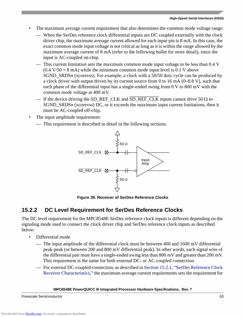
MPC8548E PowerQUICC III Integrated Processor Hardware Specifications, Rev. 7
Freescale Semiconductor 63
High-Speed Serial Interfaces (HSSI)
• The maximum average current requirement that also determines the common mode voltage range:— When the SerDes reference clock differential inputs are DC coupled externally with the clock
driver chip, the maximum average current allowed for each input pin is 8 mA. In this case, the exact common mode input voltage is not critical as long as it is within the range allowed by the maximum average current of 8 mA (refer to the following bullet for more detail), since the input is AC-coupled on-chip.
— This current limitation sets the maximum common mode input voltage to be less than 0.4 V (0.4 V/50 = 8 mA) while the minimum common mode input level is 0.1 V above SGND_SRDSn (xcorevss). For example, a clock with a 50/50 duty cycle can be produced by a clock driver with output driven by its current source from 0 to 16 mA (0–0.8 V), such that each phase of the differential input has a single-ended swing from 0 V to 800 mV with the common mode voltage at 400 mV.
— If the device driving the SD_REF_CLK and SD_REF_CLK inputs cannot drive 50 Ω to SGND_SRDSn (xcorevss) DC, or it exceeds the maximum input current limitations, then it must be AC-coupled off-chip.
• The input amplitude requirement:— This requirement is described in detail in the following sections.
Figure 39. Receiver of SerDes Reference Clocks
15.2.2 DC Level Requirement for SerDes Reference ClocksThe DC level requirement for the MPC8548E SerDes reference clock inputs is different depending on the signaling mode used to connect the clock driver chip and SerDes reference clock inputs as described below:
• Differential mode— The input amplitude of the differential clock must be between 400 and 1600 mV differential
peak-peak (or between 200 and 800 mV differential peak). In other words, each signal wire of the differential pair must have a single-ended swing less than 800 mV and greater than 200 mV. This requirement is the same for both external DC- or AC-coupled connection.
— For external DC-coupled connection, as described in Section 15.2.1, “SerDes Reference Clock Receiver Characteristics,” the maximum average current requirements sets the requirement for
InputAmp
50 Ω
50 Ω
SD_REF_CLK
SD_REF_CLK
Downloaded from Elcodis.com electronic components distributor
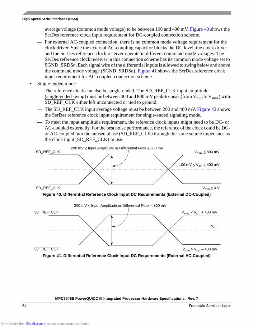
MPC8548E PowerQUICC III Integrated Processor Hardware Specifications, Rev. 7
64 Freescale Semiconductor
High-Speed Serial Interfaces (HSSI)
average voltage (common mode voltage) to be between 100 and 400 mV. Figure 40 shows the SerDes reference clock input requirement for DC-coupled connection scheme.
— For external AC-coupled connection, there is no common mode voltage requirement for the clock driver. Since the external AC-coupling capacitor blocks the DC level, the clock driver and the SerDes reference clock receiver operate in different command mode voltages. The SerDes reference clock receiver in this connection scheme has its common mode voltage set to SGND_SRDSn. Each signal wire of the differential inputs is allowed to swing below and above the command mode voltage (SGND_SRDSn). Figure 41 shows the SerDes reference clock input requirement for AC-coupled connection scheme.
• Single-ended mode— The reference clock can also be single-ended. The SD_REF_CLK input amplitude
(single-ended swing) must be between 400 and 800 mV peak-to-peak (from Vmin to Vmax) with SD_REF_CLK either left unconnected or tied to ground.
— The SD_REF_CLK input average voltage must be between 200 and 400 mV. Figure 42 shows the SerDes reference clock input requirement for single-ended signaling mode.
— To meet the input amplitude requirement, the reference clock inputs might need to be DC- or AC-coupled externally. For the best noise performance, the reference of the clock could be DC- or AC-coupled into the unused phase (SD_REF_CLK) through the same source impedance as the clock input (SD_REF_CLK) in use.
Figure 40. Differential Reference Clock Input DC Requirements (External DC-Coupled)
Figure 41. Differential Reference Clock Input DC Requirements (External AC-Coupled)
SD_REF_CLK
SD_REF_CLK
Vmax < 800 mV
Vmin > 0 V
100 mV < Vcm < 400 mV
200 mV < Input Amplitude or Differential Peak < 800 mVSD_REF_CLK
SD_REF_CLK
SD_REF_CLK
Vcm
200 mV < Input Amplitude or Differential Peak < 800 mV
Vmax < Vcm + 400 mV
Vmin > Vcm – 400 mV
Downloaded from Elcodis.com electronic components distributor

MPC8548E PowerQUICC III Integrated Processor Hardware Specifications, Rev. 7
Freescale Semiconductor 65
High-Speed Serial Interfaces (HSSI)
Figure 42. Single-Ended Reference Clock Input DC Requirements
15.2.3 Interfacing with Other Differential Signaling Levels• With on-chip termination to SGND_SRDSn (xcorevss), the differential reference clocks inputs are
HCSL (high-speed current steering logic) compatible DC-coupled. • Many other low voltage differential type outputs like LVDS (low voltage differential signaling) can
be used but may need to be AC-coupled due to the limited common mode input range allowed (100 to 400 mV) for DC-coupled connection.
• LVPECL outputs can produce signal with too large amplitude and may need to be DC-biased at clock driver output first, then followed with series attenuation resistor to reduce the amplitude, in addition to AC-coupling.
NOTEFigure 43 through Figure 46 below are for conceptual reference only. Due to the fact that clock driver chip's internal structure, output impedance, and termination requirements are different between various clock driver chip manufacturers, it is very possible that the clock circuit reference designs provided by clock driver chip vendor are different from what is shown below. They might also vary from one vendor to the other. Therefore, Freescale Semiconductor can neither provide the optimal clock driver reference circuits, nor guarantee the correctness of the following clock driver connection reference circuits. The system designer is recommended to contact the selected clock driver chip vendor for the optimal reference circuits with the MPC8548E SerDes reference clock receiver requirement provided in this document.
SD_REF_CLK
SD_REF_CLK
400 mV < SD_REF_CLK Input Amplitude < 800 mV
0 V
Downloaded from Elcodis.com electronic components distributor

MPC8548E PowerQUICC III Integrated Processor Hardware Specifications, Rev. 7
66 Freescale Semiconductor
High-Speed Serial Interfaces (HSSI)
Figure 43 shows the SerDes reference clock connection reference circuits for HCSL type clock driver. It assumes that the DC levels of the clock driver chip is compatible with MPC8548E SerDes reference clock input’s DC requirement.
Figure 43. DC-Coupled Differential Connection with HCSL Clock Driver (Reference Only)
Figure 44 shows the SerDes reference clock connection reference circuits for LVDS type clock driver. Since LVDS clock driver’s common mode voltage is higher than the MPC8548E SerDes reference clock input’s allowed range (100–400 mV), AC-coupled connection scheme must be used. It assumes the LVDS output driver features 50-Ω termination resistor. It also assumes that the LVDS transmitter establishes its own common mode level without relying on the receiver or other external component.
Figure 44. AC-Coupled Differential Connection with LVDS Clock Driver (Reference Only)
Figure 45 shows the SerDes reference clock connection reference circuits for LVPECL type clock driver. Since LVPECL driver’s DC levels (both common mode voltages and output swing) are incompatible with the MPC8548E SerDes reference clock input’s DC requirement, AC-coupling has to be used. Figure 45 assumes that the LVPECL clock driver’s output impedance is 50 Ω. R1 is used to DC-bias the LVPECL
50 Ω
50 ΩSD_REF_CLK
SD_REF_CLK
Clock Driver 100 Ω Differential PWB Trace
Clock driver vendor dependent source termination resistor
CLK_Out
CLK_Out
HCSL CLK Driver Chip
33 Ω
33 Ω
Total 50 Ω. Assume clock driver’s output impedance is about 16 Ω.
MPC8548E
CLK_Out
SerDes Refer. CLK ReceiverClock Driver
SD_REF_CLK
SD_REF_CLK
Clock Driver 100 Ω Differential PWB Trace
CLK_Out
CLK_Out
LVDS CLK Driver Chip
10 nF
10 nF
MPC8548E
SerDes Refer. CLK Receiver
50 Ω
50 Ω
Clock Driver
Downloaded from Elcodis.com electronic components distributor

MPC8548E PowerQUICC III Integrated Processor Hardware Specifications, Rev. 7
Freescale Semiconductor 67
High-Speed Serial Interfaces (HSSI)
outputs prior to AC-coupling. Its value could be ranged from 140 to 240 Ω depending on the clock driver vendor’s requirement. R2 is used together with the SerDes reference clock receiver’s 50-Ω termination resistor to attenuate the LVPECL output’s differential peak level such that it meets the MPC8548E SerDes reference clock’s differential input amplitude requirement (between 200 and 800 mV differential peak). For example, if the LVPECL output’s differential peak is 900 mV and the desired SerDes reference clock input amplitude is selected as 600 mV, the attenuation factor is 0.67, which requires R2 = 25 Ω. Consult a clock driver chip manufacturer to verify whether this connection scheme is compatible with a particular clock driver chip.
Figure 45. AC-Coupled Differential Connection with LVPECL Clock Driver (Reference Only)
Figure 46 shows the SerDes reference clock connection reference circuits for a single-ended clock driver. It assumes the DC levels of the clock driver are compatible with the MPC8548E SerDes reference clock input’s DC requirement.
Figure 46. Single-Ended Connection (Reference Only)
SD_REF_CLK
SD_REF_CLK
Clock Driver 100 Ω Differential PWB TraceSerDes Refer. CLK ReceiverClock Driver
CLK_Out
CLK_Out
LVPECL CLK Driver Chip
R2
R2
MPC8548E
10 nF
10 nF
CLK_Out
CLK_Out
R2
R2
R1Clock Driver
50 Ω
50 Ω
R1
SD_REF_CLK
SD_REF_CLK
100 Ω Differential PWB Trace
Clock Driver
CLK_Out
Single-Ended CLK Driver Chip
MPC8548E
33 Ω
Total 50 Ω. Assume clock driver’s output impedance is about 16 Ω.
50 Ω
SerDes Refer. CLK Receiver
50 Ω
50 Ω
Downloaded from Elcodis.com electronic components distributor

MPC8548E PowerQUICC III Integrated Processor Hardware Specifications, Rev. 7
68 Freescale Semiconductor
PCI Express
15.2.4 AC Requirements for SerDes Reference ClocksThe clock driver selected should provide a high quality reference clock with low phase noise and cycle-to-cycle jitter. Phase noise less than 100 kHz can be tracked by the PLL and data recovery loops and is less of a problem. Phase noise above 15 MHz is filtered by the PLL. The most problematic phase noise occurs in the 1–15 MHz range. The source impedance of the clock driver should be 50 Ω to match the transmission line and reduce reflections which are a source of noise to the system.
The detailed AC requirements of the SerDes reference clocks is defined by each interface protocol based on application usage. Refer to the following sections for detailed information:
• Section 16.2, “AC Requirements for PCI Express SerDes Clocks”• Section 17.2, “AC Requirements for Serial RapidIO SD_REF_CLK and SD_REF_CLK”
15.2.4.1 Spread Spectrum Clock
SD_REF_CLK/SD_REF_CLK are designed to work with a spread spectrum clock (+0% to –0.5% spreading at 30–33 kHz rate is allowed), assuming both ends have same reference clock. For better results, a source without significant unintended modulation should be used.
15.3 SerDes Transmitter and Receiver Reference CircuitsFigure 47 shows the reference circuits for SerDes data lane’s transmitter and receiver.
Figure 47. SerDes Transmitter and Receiver Reference Circuits
The DC and AC specification of SerDes data lanes are defined in each interface protocol section below (PCI Express, Serial Rapid IO, or SGMII) in this document based on the application usage:
• Section 16, “PCI Express”• Section 17, “Serial RapidIO”
Note that external an AC coupling capacitor is required for the above three serial transmission protocols with the capacitor value defined in the specification of each protocol section.
16 PCI ExpressThis section describes the DC and AC electrical specifications for the PCI Express bus of the MPC8548E.
SD_TXn
SD_TXn SD_RXn
SD_RXn
50 ΩReceiverTransmitter
50 Ω
50 Ω
50 Ω
Downloaded from Elcodis.com electronic components distributor

MPC8548E PowerQUICC III Integrated Processor Hardware Specifications, Rev. 7
Freescale Semiconductor 69
PCI Express
16.1 DC Requirements for PCI Express SD_REF_CLK and SD_REF_CLK
For more information, see Section 15.2, “SerDes Reference Clocks.”
16.2 AC Requirements for PCI Express SerDes ClocksTable 51 lists the AC requirements for the PCI Express SerDes clocks.
16.3 Clocking DependenciesThe ports on the two ends of a link must transmit data at a rate that is within 600 parts per million (ppm) of each other at all times. This is specified to allow bit rate clock sources with a ±300 ppm tolerance.
16.4 Physical Layer SpecificationsThe following is a summary of the specifications for the physical layer of PCI Express on this device. For further details as well as the specifications of the transport and data link layer refer to PCI Express Base Specification. Rev. 1.0a.
16.4.1 Differential Transmitter (TX) Output Table 52 defines the specifications for the differential output at all transmitters (TXs). The parameters are specified at the component pins.
Table 51. SD_REF_CLK and SD_REF_CLK AC Requirements
Symbol Parameter Description Min Typ Max Unit Notes
tREF REFCLK cycle time — 10 — ns 1
tREFCJ REFCLK cycle-to-cycle jitter. Difference in the period of any two adjacent REFCLK cycles.
— — 100 ps —
tREFPJ Phase jitter. Deviation in edge location with respect to mean edge location.
–50 — 50 ps —
Note: 1. Typical based on PCI Express Specification 2.0.
Table 52. Differential Transmitter (TX) Output Specifications
Symbol Parameter Min Nom Max Unit Comments
UI Unit interval 399.88 400 400.12 ps Each UI is 400 ps ± 300 ppm. UI does not account for spread spectrum clock dictated variations. See Note 1.
VTX-DIFFp-p Differential peak-to-peak output voltage
0.8 — 1.2 V VTX-DIFFp-p = 2 × |VTX-D+ – VTX-D–|. See Note 2.
Downloaded from Elcodis.com electronic components distributor

MPC8548E PowerQUICC III Integrated Processor Hardware Specifications, Rev. 7
70 Freescale Semiconductor
PCI Express
VTX-DE-RATIO De- emphasized differential
output voltage (ratio)
–3.0 –3.5 –4.0 dB Ratio of the VTX-DIFFp-p of the second and following bits after a transition divided by the VTX-DIFFp-p of the first bit after a transition. See Note 2.
TTX-EYE Minimum TX eye width
0.70 — — UI The maximum transmitter jitter can be derived as TTX-MAX-JITTER = 1 – TTX-EYE = 0.3 UI.See Notes 2 and 3.
TTX-EYE-MEDIAN-to-
MAX-JITTER
Maximum time between the
jitter median and maximum
deviation from the median.
— — 0.15 UI Jitter is defined as the measurement variation of the crossing points (VTX-DIFFp-p = 0 V) in relation to a recovered TX UI. A recovered TX UI is calculated over 3500 consecutive unit intervals of sample data. Jitter is measured using all edges of the 250 consecutive UI in the center of the 3500 UI used for calculating the TX UI. See Notes 2 and 3.
TTX-RISE, TTX-FALL D+/D– TX output rise/fall time
0.125 — — UI See Notes 2 and 5.
VTX-CM-ACp RMS AC peak common mode output voltage
— — 20 mV VTX-CM-ACp = RMS(|VTXD+ + VTXD–|/2 – VTX-CM-DC)VTX-CM-DC = DC(avg) of |VTX-D+ + VTX-D–|/2. See Note 2.
VTX-CM-DC-ACTIVE-
IDLE-DELTA
Absolute delta of dc common
mode voltage during L0 and electrical idle
0 — 100 mV |VTX-CM-DC (during L0) + VTX-CM-Idle-DC (during
electrical idle)| ≤ 100 mVVTX-CM-DC = DC(avg) of |VTX-D+ + VTX-D–|/2 [L0]VTX-CM-Idle-DC = DC(avg) of |VTX-D+ + VTX-D–|/2 [electrical idle] See Note 2.
VTX-CM-DC-LINE-DELTA Absolute delta of DC common
mode between D+ and D–
0 — 25 mV |VTX-CM-DC-D+ – VTX-CM-DC-D–| ≤ 25 mVVTX-CM-DC-D+ = DC(avg) of |VTX-D+|VTX-CM-DC-D–= DC(avg) of |VTX-D–|.See Note 2.
VTX-IDLE-DIFFp Electrical idle differential peak output voltage
0 — 20 mV VTX-IDLE-DIFFp = |VTX-IDLE-D+ – VTX-IDLE-D–| ≤ 20 mV.See Note 2.
VTX-RCV-DETECT The amount of voltage change allowed during
receiver detection
— — 600 mV The total amount of voltage change that a transmitter can apply to sense whether a low impedance receiver is present. See Note 6.
VTX-DC-CM The TX DC common mode
voltage
0 — 3.6 V The allowed DC common mode voltage under any conditions. See Note 6.
ITX-SHORT TX short circuit current limit
— — 90 mA The total current the transmitter can provide when shorted to its ground
Table 52. Differential Transmitter (TX) Output Specifications (continued)
Symbol Parameter Min Nom Max Unit Comments
Downloaded from Elcodis.com electronic components distributor

MPC8548E PowerQUICC III Integrated Processor Hardware Specifications, Rev. 7
Freescale Semiconductor 71
PCI Express
TTX-IDLE-MIN Minimum time spent in
electrical idle
50 — UI Minimum time a transmitter must be in electrical idle utilized by the receiver to start looking for an electrical idle exit after successfully receiving an electrical idle ordered set
TTX-IDLE-SET-TO-IDLE Maximum time to transition to a valid electrical
idle after sending an
electrical idle ordered set
— — 20 UI After sending an electrical idle ordered set, the transmitter must meet all electrical idle specifications within this time. This is considered a debounce time for the transmitter to meet electrical idle after transitioning from L0.
TTX-IDLE-TO-DIFF-DATA Maximum time to transition to
valid TX specifications
after leaving an electrical idle
condition
— — 20 UI Maximum time to meet all TX specifications when transitioning from electrical idle to sending differential data. This is considered a debounce time for the TX to meet all TX specifications after leaving electrical idle
RLTX-DIFF Differential return loss
12 — — dB Measured over 50 MHz to 1.25 GHz. See Note 4.
RLTX-CM Common mode return loss
6 — — dB Measured over 50 MHz to 1.25 GHz. See Note 4.
ZTX-DIFF-DC DC differential TX impedance
80 100 120 Ω TX DC differential mode low impedance
ZTX-DC Transmitter DC impedance
40 — — Ω Required TX D+ as well as D– DC impedance during all states
LTX-SKEW Lane-to-lane output skew
— — 500 + 2 UI
ps Static skew between any two transmitter lanes within a single Link
CTX AC coupling capacitor
75 — 200 nF All transmitters shall be AC coupled. The AC coupling is required either within the media or within the transmitting component itself. See note 8.
Table 52. Differential Transmitter (TX) Output Specifications (continued)
Symbol Parameter Min Nom Max Unit Comments
Downloaded from Elcodis.com electronic components distributor

MPC8548E PowerQUICC III Integrated Processor Hardware Specifications, Rev. 7
72 Freescale Semiconductor
PCI Express
16.4.2 Transmitter Compliance Eye DiagramsThe TX eye diagram in Figure 48 is specified using the passive compliance/test measurement load (see Figure 50) in place of any real PCI Express interconnect +RX component.
There are two eye diagrams that must be met for the transmitter. Both eye diagrams must be aligned in time using the jitter median to locate the center of the eye diagram. The different eye diagrams differ in voltage depending whether it is a transition bit or a de-emphasized bit. The exact reduced voltage level of the de-emphasized bit is always relative to the transition bit.
The eye diagram must be valid for any 250 consecutive UIs.
A recovered TX UI is calculated over 3500 consecutive unit intervals of sample data. The eye diagram is created using all edges of the 250 consecutive UI in the center of the 3500 UI used for calculating the TX UI.
NOTEIt is recommended that the recovered TX UI is calculated using all edges in the 3500 consecutive UI interval with a fit algorithm using a minimization merit function (for example, least squares and median deviation fits).
Tcrosslink Crosslink random timeout
0 — 1 ms This random timeout helps resolve conflicts in crosslink configuration by eventually resulting in only one downstream and one upstream port. See Note 7.
Notes:1. No test load is necessarily associated with this value.2. Specified at the measurement point into a timing and voltage compliance test load as shown in Figure 50 and measured over
any 250 consecutive TX UIs. (Also refer to the transmitter compliance eye diagram shown in Figure 48.)3. A TTX-EYE = 0.70 UI provides for a total sum of deterministic and random jitter budget of TTX-JITTER-MAX = 0.30 UI for the
transmitter collected over any 250 consecutive TX UIs. The TTX-EYE-MEDIAN-to-MAX-JITTER median is less than half of the total TX jitter budget collected over any 250 consecutive TX UIs. It should be noted that the median is not the same as the mean. The jitter median describes the point in time where the number of jitter points on either side is approximately equal as opposed to the averaged time value.
4. The transmitter input impedance shall result in a differential return loss greater than or equal to 12 dB and a common mode return loss greater than or equal to 6 dB over a frequency range of 50 MHz to 1.25 GHz. This input impedance requirement applies to all valid input levels. The reference impedance for return loss measurements is 50 Ω to ground for both the D+ and D– line (that is, as measured by a vector network analyzer with 50-Ω probes—see Figure 50). Note that the series capacitors CTX is optional for the return loss measurement.
5. Measured between 20%–80% at transmitter package pins into a test load as shown in Figure 50 for both VTX-D+ and VTX-D–. 6. See Section 4.3.1.8 of the PCI Express Base Specifications Rev 1.0a.7. See Section 4.2.6.3 of the PCI Express Base Specifications Rev 1.0a.8. MPC8548E SerDes transmitter does not have CTX built in. An external AC coupling capacitor is required.
Table 52. Differential Transmitter (TX) Output Specifications (continued)
Symbol Parameter Min Nom Max Unit Comments
Downloaded from Elcodis.com electronic components distributor

MPC8548E PowerQUICC III Integrated Processor Hardware Specifications, Rev. 7
Freescale Semiconductor 73
PCI Express
Figure 48. Minimum Transmitter Timing and Voltage Output Compliance Specifications
16.4.3 Differential Receiver (RX) Input SpecificationsTable 53 defines the specifications for the differential input at all receivers (RXs). The parameters are specified at the component pins.
Table 53. Differential Receiver (RX) Input Specifications
Symbol Parameter Min Nom Max Unit Comments
UI Unit interval 399.88 400 400.12 ps Each UI is 400 ps ± 300 ppm. UI does not account for spread spectrum clock dictated variations. See Note 1.
VRX-DIFFp-p Differential peak-to-peak input voltage
0.175 — 1.200 V VRX-DIFFp-p = 2 × |VRX-D+ – VRX-D–|. See Note 2.
TRX-EYE Minimum receiver eye
width
0.4 — — UI The maximum interconnect media and transmitter jitter that can be tolerated by the receiver can be derived as TRX-MAX-JITTER = 1 – TRX-EYE = 0.6 UI.See Notes 2 and 3.
TRX-EYE-MEDIAN-to-
MAX-JITTER
Maximum time between the
jitter median and maximum
deviation from the median
— — 0.3 UI Jitter is defined as the measurement variation of the crossing points (VRX-DIFFp-p = 0 V) in relation to a recovered TX UI. A recovered TX UI is calculated over 3500 consecutive unit intervals of sample data. Jitter is measured using all edges of the 250 consecutive UI in the center of the 3500 UI used for calculating the TX UI. See Notes 2, 3, and 7.
VTX-DIFF = 0 mV(D+ D– Crossing Point)
[De-Emphasized Bit]
0.07 UI = UI – 0.3 UI (JTX-TOTAL-MAX)
566 mV (3 dB) >= VTX-DIFFp-p-MIN >= 505 mV (4 dB)
[Transition Bit]VTX-DIFFp-p-MIN = 800 mV
VRX-DIFF = 0 mV(D+ D– Crossing Point)
[Transition Bit]VTX-DIFFp-p-MIN = 800 mV
Downloaded from Elcodis.com electronic components distributor

MPC8548E PowerQUICC III Integrated Processor Hardware Specifications, Rev. 7
74 Freescale Semiconductor
PCI Express
VRX-CM-ACp AC peak common mode input voltage
— — 150 mV VRX-CM-ACp = |VRXD+ – VRXD-|/2 + VRX-CM-DCVRX-CM-DC = DC(avg) of |VRX-D+ + VRX-D–| ÷ 2. See Note 2.
RLRX-DIFF Differential return loss
15 — — dB Measured over 50 MHz to 1.25 GHz with the D+ and D– lines biased at +300 mV and –300 mV, respectively. See Note 4.
RLRX-CM Common mode return loss
6 — — dB Measured over 50 MHz to 1.25 GHz with the D+ and D– lines biased at 0 V. See Note 4.
ZRX-DIFF-DC DC differential input impedance
80 100 120 Ω RX DC differential mode impedance. See Note 5.
ZRX-DC DC input impedance
40 50 60 Ω Required RX D+ as well as D– DC impedance (50 ± 20% tolerance). See Notes 2 and 5.
ZRX-HIGH-IMP-DC Powered down DC input
impedance
200 k — — Ω Required RX D+ as well as D– DC impedance when the receiver terminations do not have power. See Note 6.
VRX-IDLE-DET-DIFFp-p Electrical idle detect threshold
65 — 175 mV VRX-IDLE-DET-DIFFp-p = 2 × |VRX-D+ –VRX-D–|. Measured at the package pins of the receiver
TRX-IDLE-DET-DIFF-
ENTERTIME
Unexpected electrical idle enter detect
threshold integration time
— — 10 ms An unexpected electrical idle (VRX-DIFFp-p < VRX-IDLE-DET-DIFFp-p) must be recognized no longer than TRX-IDLE-DET-DIFF-ENTERING to signal an unexpected idle condition.
Table 53. Differential Receiver (RX) Input Specifications (continued)
Symbol Parameter Min Nom Max Unit Comments
Downloaded from Elcodis.com electronic components distributor

MPC8548E PowerQUICC III Integrated Processor Hardware Specifications, Rev. 7
Freescale Semiconductor 75
PCI Express
16.5 Receiver Compliance Eye DiagramsThe RX eye diagram in Figure 49 is specified using the passive compliance/test measurement load (see Figure 50) in place of any real PCI Express RX component.
Note: In general, the minimum receiver eye diagram measured with the compliance/test measurement load (see Figure 50) is larger than the minimum receiver eye diagram measured over a range of systems at the input receiver of any real PCI Express component. The degraded eye diagram at the input receiver is due to traces internal to the package as well as silicon parasitic characteristics which cause the real PCI Express component to vary in impedance from the compliance/test measurement load. The input receiver eye diagram is implementation specific and is not specified. RX component designer should provide additional margin to adequately compensate for the degraded minimum receiver eye diagram (shown in Figure 49) expected at the input receiver based on some adequate combination of system simulations and the return loss measured looking into the RX package and silicon. The RX eye diagram must be aligned in time using the jitter median to locate the center of the eye diagram.
LTX-SKEW Total Skew — — 20 ns Skew across all lanes on a Link. This includes variation in the length of SKP ordered set (for example, COM and one to five symbols) at the RX as well as any delay differences arising from the interconnect itself.
Notes:1. No test load is necessarily associated with this value.2. Specified at the measurement point and measured over any 250 consecutive UIs. The test load in Figure 50 should be used
as the RX device when taking measurements (also refer to the receiver compliance eye diagram shown in Figure 49). If the clocks to the RX and TX are not derived from the same reference clock, the TX UI recovered from 3500 consecutive UI must be used as a reference for the eye diagram.
3. A TRX-EYE = 0.40 UI provides for a total sum of 0.60 UI deterministic and random jitter budget for the transmitter and interconnect collected any 250 consecutive UIs. The TRX-EYE-MEDIAN-to-MAX-JITTER specification ensures a jitter distribution in which the median and the maximum deviation from the median is less than half of the total. UI jitter budget collected over any 250 consecutive TX UIs. It should be noted that the median is not the same as the mean. The jitter median describes the point in time where the number of jitter points on either side is approximately equal as opposed to the averaged time value. If the clocks to the RX and TX are not derived from the same reference clock, the TX UI recovered from 3500 consecutive UI must be used as the reference for the eye diagram.
4. The receiver input impedance shall result in a differential return loss greater than or equal to 15 dB with the D+ line biased to 300 mV and the D– line biased to –{300 mV and a common mode return loss greater than or equal to 6 dB (no bias required) over a frequency range of 50 MHz to 1.25 GHz. This input impedance requirement applies to all valid input levels. The reference impedance for return loss measurements for is 50 Ω to ground for both the D+ and D– line (that is, as measured by a vector network analyzer with 50-Ω probes—see Figure 50). Note: that the series capacitors CTX is optional for the return loss measurement.
5. Impedance during all LTSSM states. When transitioning from a fundamental reset to detect (the initial state of the LTSSM) there is a 5 ms transition time before receiver termination values must be met on all unconfigured lanes of a port.
6. The RX DC common mode Impedance that exists when no power is present or fundamental reset is asserted. This helps ensure that the receiver detect circuit does not falsely assume a receiver is powered on when it is not. This term must be measured at 300 mV above the RX ground.
7. It is recommended that the recovered TX UI is calculated using all edges in the 3500 consecutive UI interval with a fit algorithm using a minimization merit function. Least squares and median deviation fits have worked well with experimental and simulated data.
Table 53. Differential Receiver (RX) Input Specifications (continued)
Symbol Parameter Min Nom Max Unit Comments
Downloaded from Elcodis.com electronic components distributor

MPC8548E PowerQUICC III Integrated Processor Hardware Specifications, Rev. 7
76 Freescale Semiconductor
PCI Express
The eye diagram must be valid for any 250 consecutive UIs.
A recovered TX UI is calculated over 3500 consecutive unit intervals of sample data. The eye diagram is created using all edges of the 250 consecutive UI in the center of the 3500 UI used for calculating the TX UI.
NOTEThe reference impedance for return loss measurements is 50. to ground for both the D+ and D– line (that is, as measured by a vector network analyzer with 50-Ω probes—see Figure 50). Note that the series capacitors, CTX, are optional for the return loss measurement.
Figure 49. Minimum Receiver Eye Timing and Voltage Compliance Specification
16.5.1 Compliance Test and Measurement LoadThe AC timing and voltage parameters must be verified at the measurement point, as specified within 0.2 inches of the package pins, into a test/measurement load shown in Figure 50.
NOTEThe allowance of the measurement point to be within 0.2 inches of the package pins is meant to acknowledge that package/board routing may benefit from D+ and D– not being exactly matched in length at the package pin boundary.
Figure 50. Compliance Test/Measurement Load
VRX-DIFF = 0 mV(D+ D– Crossing Point)
VRX-DIFF = 0 mV(D+ D– Crossing Point)
VRX-DIFFp-p-MIN > 175 mV
0.4 UI = TRX-EYE-MIN
TXSilicon
+ Package
C = CTX
C = CTX
R = 50 Ω R = 50 Ω
D+ PackagePin
D– PackagePin
D+ PackagePin
Downloaded from Elcodis.com electronic components distributor
MPC8548E PowerQUICC III Integrated Processor Hardware Specifications, Rev. 7
Freescale Semiconductor 77
Serial RapidIO
17 Serial RapidIOThis section describes the DC and AC electrical specifications for the RapidIO interface of the MPC8548E, for the LP-Serial physical layer. The electrical specifications cover both single- and multiple-lane links. Two transmitters (short and long run) and a single receiver are specified for each of three baud rates, 1.25, 2.50, and 3.125 GBaud.
Two transmitter specifications allow for solutions ranging from simple board-to-board interconnect to driving two connectors across a backplane. A single receiver specification is given that accepts signals from both the short- and long-run transmitter specifications.
The short-run transmitter should be used mainly for chip-to-chip connections on either the same printed-circuit board or across a single connector. This covers the case where connections are made to a mezzanine (daughter) card. The minimum swings of the short-run specification reduce the overall power used by the transceivers.
The long-run transmitter specifications use larger voltage swings that are capable of driving signals across backplanes. This allows a user to drive signals across two connectors and a backplane. The specifications allow a distance of at least 50 cm at all baud rates.
All unit intervals are specified with a tolerance of ±100 ppm. The worst case frequency difference between any transmit and receive clock is 200 ppm.
To ensure interoperability between drivers and receivers of different vendors and technologies, AC coupling at the receiver input must be used.
17.1 DC Requirements for Serial RapidIO SD_REF_CLK and SD_REF_CLK
For more information, see Section 15.2, “SerDes Reference Clocks.”
17.2 AC Requirements for Serial RapidIO SD_REF_CLK and SD_REF_CLK
Table 54 lists the Serial RapidIO SD_REF_CLK and SD_REF_CLK AC requirements.Table 54. SD_REF_CLK and SD_REF_CLK AC Requirements
Symbol Parameter Description Min Typ Max Unit Comments
tREF REFCLK cycle time — 10(8) — ns 8 ns applies only to serial RapidIO with 125-MHz reference clock
tREFCJ REFCLK cycle-to-cycle jitter. Difference in the period of any two adjacent REFCLK cycles.
— — 80 ps —
tREFPJ Phase jitter. Deviation in edge location with respect to mean edge location.
–40 — 40 ps —
Downloaded from Elcodis.com electronic components distributor
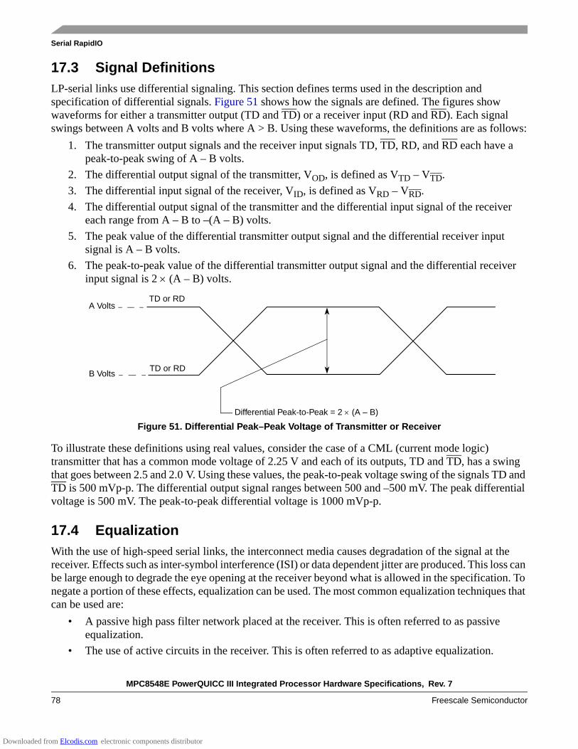
MPC8548E PowerQUICC III Integrated Processor Hardware Specifications, Rev. 7
78 Freescale Semiconductor
Serial RapidIO
17.3 Signal DefinitionsLP-serial links use differential signaling. This section defines terms used in the description and specification of differential signals. Figure 51 shows how the signals are defined. The figures show waveforms for either a transmitter output (TD and TD) or a receiver input (RD and RD). Each signal swings between A volts and B volts where A > B. Using these waveforms, the definitions are as follows:
1. The transmitter output signals and the receiver input signals TD, TD, RD, and RD each have a peak-to-peak swing of A – B volts.
2. The differential output signal of the transmitter, VOD, is defined as VTD – VTD.3. The differential input signal of the receiver, VID, is defined as VRD – VRD.4. The differential output signal of the transmitter and the differential input signal of the receiver
each range from A – B to –(A – B) volts.5. The peak value of the differential transmitter output signal and the differential receiver input
signal is A – B volts.6. The peak-to-peak value of the differential transmitter output signal and the differential receiver
input signal is 2 × (A – B) volts.
Figure 51. Differential Peak–Peak Voltage of Transmitter or Receiver
To illustrate these definitions using real values, consider the case of a CML (current mode logic) transmitter that has a common mode voltage of 2.25 V and each of its outputs, TD and TD, has a swing that goes between 2.5 and 2.0 V. Using these values, the peak-to-peak voltage swing of the signals TD and TD is 500 mVp-p. The differential output signal ranges between 500 and –500 mV. The peak differential voltage is 500 mV. The peak-to-peak differential voltage is 1000 mVp-p.
17.4 EqualizationWith the use of high-speed serial links, the interconnect media causes degradation of the signal at the receiver. Effects such as inter-symbol interference (ISI) or data dependent jitter are produced. This loss can be large enough to degrade the eye opening at the receiver beyond what is allowed in the specification. To negate a portion of these effects, equalization can be used. The most common equalization techniques that can be used are:
• A passive high pass filter network placed at the receiver. This is often referred to as passive equalization.
• The use of active circuits in the receiver. This is often referred to as adaptive equalization.
Differential Peak-to-Peak = 2 × (A – B)
A VoltsTD or RD
TD or RDB Volts
Downloaded from Elcodis.com electronic components distributor
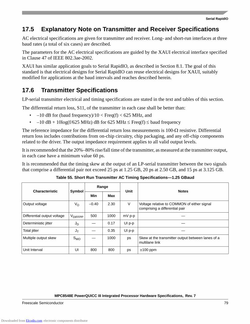
MPC8548E PowerQUICC III Integrated Processor Hardware Specifications, Rev. 7
Freescale Semiconductor 79
Serial RapidIO
17.5 Explanatory Note on Transmitter and Receiver SpecificationsAC electrical specifications are given for transmitter and receiver. Long- and short-run interfaces at three baud rates (a total of six cases) are described.
The parameters for the AC electrical specifications are guided by the XAUI electrical interface specified in Clause 47 of IEEE 802.3ae-2002.
XAUI has similar application goals to Serial RapidIO, as described in Section 8.1. The goal of this standard is that electrical designs for Serial RapidIO can reuse electrical designs for XAUI, suitably modified for applications at the baud intervals and reaches described herein.
17.6 Transmitter SpecificationsLP-serial transmitter electrical and timing specifications are stated in the text and tables of this section.
The differential return loss, S11, of the transmitter in each case shall be better than:• –10 dB for (baud frequency)/10 < Freq(f) < 625 MHz, and• –10 dB + 10log(f/625 MHz) dB for 625 MHz ≤ Freq(f) ≤ baud frequency
The reference impedance for the differential return loss measurements is 100-Ω resistive. Differential return loss includes contributions from on-chip circuitry, chip packaging, and any off-chip components related to the driver. The output impedance requirement applies to all valid output levels.
It is recommended that the 20%–80% rise/fall time of the transmitter, as measured at the transmitter output, in each case have a minimum value 60 ps.
It is recommended that the timing skew at the output of an LP-serial transmitter between the two signals that comprise a differential pair not exceed 25 ps at 1.25 GB, 20 ps at 2.50 GB, and 15 ps at 3.125 GB.
Table 55. Short Run Transmitter AC Timing Specifications—1.25 GBaud
Characteristic SymbolRange
Unit NotesMin Max
Output voltage VO –0.40 2.30 V Voltage relative to COMMON of either signal comprising a differential pair
Differential output voltage VDIFFPP 500 1000 mV p-p —
Deterministic jitter JD — 0.17 UI p-p —
Total jitter JT — 0.35 UI p-p —
Multiple output skew SMO — 1000 ps Skew at the transmitter output between lanes of a multilane link
Unit Interval UI 800 800 ps ±100 ppm
Downloaded from Elcodis.com electronic components distributor
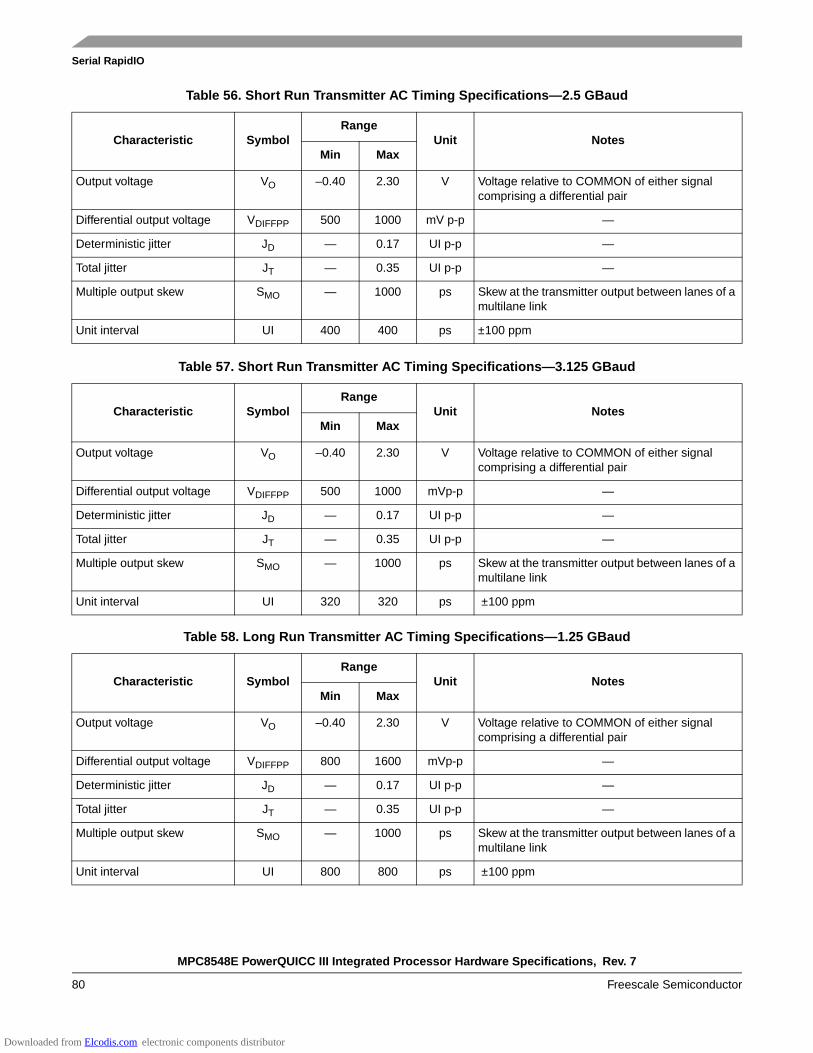
MPC8548E PowerQUICC III Integrated Processor Hardware Specifications, Rev. 7
80 Freescale Semiconductor
Serial RapidIO
Table 56. Short Run Transmitter AC Timing Specifications—2.5 GBaud
Characteristic SymbolRange
Unit NotesMin Max
Output voltage VO –0.40 2.30 V Voltage relative to COMMON of either signal comprising a differential pair
Differential output voltage VDIFFPP 500 1000 mV p-p —
Deterministic jitter JD — 0.17 UI p-p —
Total jitter JT — 0.35 UI p-p —
Multiple output skew SMO — 1000 ps Skew at the transmitter output between lanes of a multilane link
Unit interval UI 400 400 ps ±100 ppm
Table 57. Short Run Transmitter AC Timing Specifications—3.125 GBaud
Characteristic SymbolRange
Unit NotesMin Max
Output voltage VO –0.40 2.30 V Voltage relative to COMMON of either signal comprising a differential pair
Differential output voltage VDIFFPP 500 1000 mVp-p —
Deterministic jitter JD — 0.17 UI p-p —
Total jitter JT — 0.35 UI p-p —
Multiple output skew SMO — 1000 ps Skew at the transmitter output between lanes of a multilane link
Unit interval UI 320 320 ps ±100 ppm
Table 58. Long Run Transmitter AC Timing Specifications—1.25 GBaud
Characteristic SymbolRange
Unit NotesMin Max
Output voltage VO –0.40 2.30 V Voltage relative to COMMON of either signal comprising a differential pair
Differential output voltage VDIFFPP 800 1600 mVp-p —
Deterministic jitter JD — 0.17 UI p-p —
Total jitter JT — 0.35 UI p-p —
Multiple output skew SMO — 1000 ps Skew at the transmitter output between lanes of a multilane link
Unit interval UI 800 800 ps ±100 ppm
Downloaded from Elcodis.com electronic components distributor

MPC8548E PowerQUICC III Integrated Processor Hardware Specifications, Rev. 7
Freescale Semiconductor 81
Serial RapidIO
For each baud rate at which an LP-serial transmitter is specified to operate, the output eye pattern of the transmitter shall fall entirely within the unshaded portion of the transmitter output compliance mask shown in Figure 52 with the parameters specified in Table 61 when measured at the output pins of the device and the device is driving a 100-Ω ± 5% differential resistive load. The output eye pattern of an LP-serial
Table 59. Long Run Transmitter AC Timing Specifications—2.5 GBaud
Characteristic SymbolRange
Unit NotesMin Max
Output voltage VO –0.40 2.30 V Voltage relative to COMMON of either signal comprising a differential pair
Differential output voltage VDIFFPP 800 1600 mVp-p —
Deterministic jitter JD — 0.17 UI p-p —
Total jitter JT — 0.35 UI p-p —
Multiple output skew SMO — 1000 ps Skew at the transmitter output between lanes of a multilane link
Unit interval UI 400 400 ps ±100 ppm
Table 60. Long Run Transmitter AC Timing Specifications—3.125 GBaud
Characteristic SymbolRange
Unit NotesMin Max
Output voltage VO –0.40 2.30 V Voltage relative to COMMON of either signal comprising a differential pair
Differential output voltage VDIFFPP 800 1600 mVp-p —
Deterministic jitter JD — 0.17 UI p-p —
Total jitter JT — 0.35 UI p-p —
Multiple output skew SMO — 1000 ps Skew at the transmitter output between lanes of a multilane link
Unit interval UI 320 320 ps ±100 ppm
Downloaded from Elcodis.com electronic components distributor

MPC8548E PowerQUICC III Integrated Processor Hardware Specifications, Rev. 7
82 Freescale Semiconductor
Serial RapidIO
transmitter that implements pre-emphasis (to equalize the link and reduce inter-symbol interference) need only comply with the transmitter output compliance mask when pre-emphasis is disabled or minimized.
Figure 52. Transmitter Output Compliance Mask
17.7 Receiver SpecificationsLP-serial receiver electrical and timing specifications are stated in the text and tables of this section.
Receiver input impedance shall result in a differential return loss better that 10 dB and a common mode return loss better than 6 dB from 100 MHz to (0.8) × (baud frequency). This includes contributions from on-chip circuitry, the chip package, and any off-chip components related to the receiver. AC coupling
Table 61. Transmitter Differential Output Eye Diagram Parameters
Transmitter Type VDIFFmin (mV) VDIFFmax (mV) A (UI) B (UI)
1.25 GBaud short range 250 500 0.175 0.39
1.25 GBaud long range 400 800 0.175 0.39
2.5 GBaud short range 250 500 0.175 0.39
2.5 GBaud long range 400 800 0.175 0.39
3.125 GBaud short range 250 500 0.175 0.39
3.125 GBaud long range 400 800 0.175 0.39
0
VDIFF min
VDIFF max
–VDIFF min
–VDIFF max
0 B 1-B 1Time in UI
Tran
smitt
er D
iffer
entia
l Out
put V
olta
ge
A 1-A
Downloaded from Elcodis.com electronic components distributor

MPC8548E PowerQUICC III Integrated Processor Hardware Specifications, Rev. 7
Freescale Semiconductor 83
Serial RapidIO
components are included in this requirement. The reference impedance for return loss measurements is 100-Ω resistive for differential return loss and 25-Ω resistive for common mode.
Table 62. Receiver AC Timing Specifications—1.25 GBaud
Characteristic SymbolRange
Unit NotesMin Max
Differential input voltage VIN 200 1600 mVp-p Measured at receiver
Deterministic jitter tolerance JD 0.37 — UI p-p Measured at receiver
Combined deterministic and random jitter tolerance
JDR 0.55 — UI p-p Measured at receiver
Total jitter tolerance1 JT 0.65 — UI p-p Measured at receiver
Multiple input skew SMI — 24 ns Skew at the receiver input between lanes of a multilane link
Bit error rate BER — 10–12 — —
Unit interval UI 800 800 ps ±100 ppm
Note: 1. Total jitter is composed of three components, deterministic jitter, random jitter, and single frequency sinusoidal jitter. The
sinusoidal jitter may have any amplitude and frequency in the unshaded region of Figure 53. The sinusoidal jitter component is included to ensure margin for low frequency jitter, wander, noise, crosstalk, and other variable system effects.
Table 63. Receiver AC Timing Specifications—2.5 GBaud
Characteristic SymbolRange
Unit NotesMin Max
Differential input voltage VIN 200 1600 mVp-p Measured at receiver
Deterministic jitter tolerance JD 0.37 — UI p-p Measured at receiver
Combined deterministic and random jitter tolerance
JDR 0.55 — UI p-p Measured at receiver
Total jitter tolerance1 JT 0.65 — UI p-p Measured at receiver
Multiple input skew SMI — 24 ns Skew at the receiver input between lanes of a multilane link
Bit error rate BER — 10–12 —
Unit interval UI 400 400 ps ±100 ppm
Note: 1. Total jitter is composed of three components, deterministic jitter, random jitter, and single frequency sinusoidal jitter. The
sinusoidal jitter may have any amplitude and frequency in the unshaded region of Figure 53. The sinusoidal jitter component is included to ensure margin for low frequency jitter, wander, noise, crosstalk, and other variable system effects.
Downloaded from Elcodis.com electronic components distributor
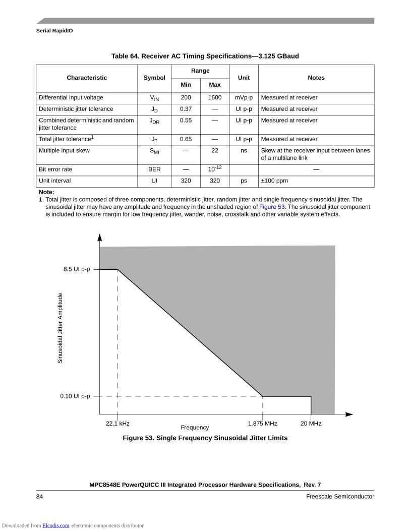
MPC8548E PowerQUICC III Integrated Processor Hardware Specifications, Rev. 7
84 Freescale Semiconductor
Serial RapidIO
Figure 53. Single Frequency Sinusoidal Jitter Limits
Table 64. Receiver AC Timing Specifications—3.125 GBaud
Characteristic SymbolRange
Unit NotesMin Max
Differential input voltage VIN 200 1600 mVp-p Measured at receiver
Deterministic jitter tolerance JD 0.37 — UI p-p Measured at receiver
Combined deterministic and random jitter tolerance
JDR 0.55 — UI p-p Measured at receiver
Total jitter tolerance1 JT 0.65 — UI p-p Measured at receiver
Multiple input skew SMI — 22 ns Skew at the receiver input between lanes of a multilane link
Bit error rate BER — 10-12 —
Unit interval UI 320 320 ps ±100 ppm
Note: 1. Total jitter is composed of three components, deterministic jitter, random jitter and single frequency sinusoidal jitter. The
sinusoidal jitter may have any amplitude and frequency in the unshaded region of Figure 53. The sinusoidal jitter component is included to ensure margin for low frequency jitter, wander, noise, crosstalk and other variable system effects.
8.5 UI p-p
0.10 UI p-p
Sin
usoi
dal J
itter
Am
plitu
de
22.1 kHz 1.875 MHz 20 MHzFrequency
Downloaded from Elcodis.com electronic components distributor
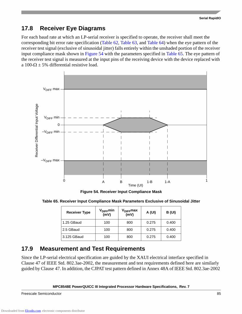
MPC8548E PowerQUICC III Integrated Processor Hardware Specifications, Rev. 7
Freescale Semiconductor 85
Serial RapidIO
17.8 Receiver Eye DiagramsFor each baud rate at which an LP-serial receiver is specified to operate, the receiver shall meet the corresponding bit error rate specification (Table 62, Table 63, and Table 64) when the eye pattern of the receiver test signal (exclusive of sinusoidal jitter) falls entirely within the unshaded portion of the receiver input compliance mask shown in Figure 54 with the parameters specified in Table 65. The eye pattern of the receiver test signal is measured at the input pins of the receiving device with the device replaced with a 100-Ω ± 5% differential resistive load.
Figure 54. Receiver Input Compliance Mask
17.9 Measurement and Test RequirementsSince the LP-serial electrical specification are guided by the XAUI electrical interface specified in Clause 47 of IEEE Std. 802.3ae-2002, the measurement and test requirements defined here are similarly guided by Clause 47. In addition, the CJPAT test pattern defined in Annex 48A of IEEE Std. 802.3ae-2002
Table 65. Receiver Input Compliance Mask Parameters Exclusive of Sinusoidal Jitter
Receiver TypeVDIFFmin
(mV)VDIFFmax
(mV)A (UI) B (UI)
1.25 GBaud 100 800 0.275 0.400
2.5 GBaud 100 800 0.275 0.400
3.125 GBaud 100 800 0.275 0.400
10
VDIFF max
–VDIFF max
VDIFF min
–VDIFF min
Time (UI)
Rec
eive
r D
iffer
entia
l Inp
ut V
olta
ge
0
A B 1-B 1-A
Downloaded from Elcodis.com electronic components distributor

MPC8548E PowerQUICC III Integrated Processor Hardware Specifications, Rev. 7
86 Freescale Semiconductor
Serial RapidIO
is specified as the test pattern for use in eye pattern and jitter measurements. Annex 48B of IEEE Std. 802.3ae-2002 is recommended as a reference for additional information on jitter test methods.
17.9.1 Eye Template MeasurementsFor the purpose of eye template measurements, the effects of a single-pole high pass filter with a 3 dB point at (baud frequency)/1667 is applied to the jitter. The data pattern for template measurements is the continuous jitter test pattern (CJPAT) defined in Annex 48A of IEEE 802.3ae. All lanes of the LP-serial link shall be active in both the transmit and receive directions, and opposite ends of the links shall use asynchronous clocks. Four lane implementations shall use CJPAT as defined in Annex 48A. Single lane implementations shall use the CJPAT sequence specified in Annex 48A for transmission on lane 0. The amount of data represented in the eye shall be adequate to ensure that the bit error ratio is less than 10–12. The eye pattern shall be measured with AC coupling and the compliance template centered at 0 V differential. The left and right edges of the template shall be aligned with the mean zero crossing points of the measured data eye. The load for this test shall be 100-Ω resistive ± 5% differential to 2.5 GHz.
17.9.2 Jitter Test MeasurementsFor the purpose of jitter measurement, the effects of a single-pole high pass filter with a 3 dB point at (baud frequency)/1667 is applied to the jitter. The data pattern for jitter measurements is the Continuous Jitter test pattern (CJPAT) pattern defined in Annex 48A of IEEE 802.3ae. All lanes of the LP-serial link shall be active in both the transmit and receive directions, and opposite ends of the links shall use asynchronous clocks. Four lane implementations shall use CJPAT as defined in Annex 48A. Single lane implementations shall use the CJPAT sequence specified in Annex 48A for transmission on lane 0. Jitter shall be measured with AC coupling and at 0 V differential. Jitter measurement for the transmitter (or for calibration of a jitter tolerance setup) shall be performed with a test procedure resulting in a BER curve such as that described in Annex 48B of IEEE 802.3ae.
17.9.3 Transmit JitterTransmit jitter is measured at the driver output when terminated into a load of 100 Ω resistive ± 5% differential to 2.5 GHz.
17.9.4 Jitter ToleranceJitter tolerance is measured at the receiver using a jitter tolerance test signal. This signal is obtained by first producing the sum of deterministic and random jitter defined in Section 17.7, “Receiver Specifications,” and then adjusting the signal amplitude until the data eye contacts the 6 points of the minimum eye opening of the receive template shown in Figure 54 and Table 65. Note that for this to occur, the test signal must have vertical waveform symmetry about the average value and have horizontal symmetry (including jitter) about the mean zero crossing. Eye template measurement requirements are as defined above. Random jitter is calibrated using a high pass filter with a low frequency corner at 20 MHz and a 20 dB/decade roll-off below this. The required sinusoidal jitter specified in Section 17.7, “Receiver Specifications,” is then added to the signal and the test load is replaced by the receiver being tested.
Downloaded from Elcodis.com electronic components distributor
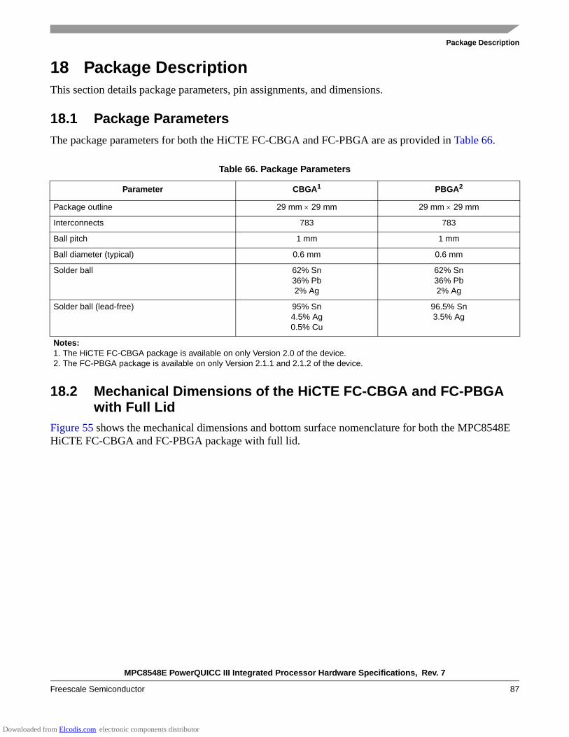
MPC8548E PowerQUICC III Integrated Processor Hardware Specifications, Rev. 7
Freescale Semiconductor 87
Package Description
18 Package DescriptionThis section details package parameters, pin assignments, and dimensions.
18.1 Package ParametersThe package parameters for both the HiCTE FC-CBGA and FC-PBGA are as provided in Table 66.
18.2 Mechanical Dimensions of the HiCTE FC-CBGA and FC-PBGA with Full Lid
Figure 55 shows the mechanical dimensions and bottom surface nomenclature for both the MPC8548E HiCTE FC-CBGA and FC-PBGA package with full lid.
Table 66. Package Parameters
Parameter CBGA1 PBGA2
Package outline 29 mm × 29 mm 29 mm × 29 mm
Interconnects 783 783
Ball pitch 1 mm 1 mm
Ball diameter (typical) 0.6 mm 0.6 mm
Solder ball 62% Sn36% Pb2% Ag
62% Sn36% Pb2% Ag
Solder ball (lead-free) 95% Sn4.5% Ag0.5% Cu
96.5% Sn3.5% Ag
Notes:1. The HiCTE FC-CBGA package is available on only Version 2.0 of the device.2. The FC-PBGA package is available on only Version 2.1.1 and 2.1.2 of the device.
Downloaded from Elcodis.com electronic components distributor

MPC8548E PowerQUICC III Integrated Processor Hardware Specifications, Rev. 7
88 Freescale Semiconductor
Package Description
Figure 55. Mechanical Dimensions and Bottom Surface Nomenclature of the HiCTEFC-CBGA and FC-PBGA with Full Lid
Notes:1. All dimensions are in millimeters.2. Dimensioning and tolerancing per ASME Y14.5M-1994.3. Maximum solder ball diameter measured parallel to datum A.4. Datum A, the seating plane, is determined by the spherical crowns of the solder balls.5. Parallelism measurement shall exclude any effect of mark on top surface of package.6. All dimensions are symmetric across the package center lines unless dimensioned otherwise.7. Package code summary:
•PBGA 8423 •CBGA 5112
SIDE VIEW
A
C
E
G
J
L
N
RU
W
AA
AC
V
Y
AB
M
P
T
F
H
K
B
D
1 3 5 7 9 11 13 15 17 19 21 232 4 6 8 10 12 14 16 18 20 22
BOTTOM VIEW
25 2724 26 28
ADAE
AFAG
AH
A1 CORNERLID CHAMFER
29 B
C
783X 0.2 A
0.25 A
0.35 A
5
A
4
SEATINGPLANE
0.60.35
1.321.08
1.631.37
3.38MAX
783X 0.7 0.5 3
0.3 M A B C0.15 A
0.5
27X 1
27X 10.5
TOP VIEW
28.7 MAXLID ZONE
4X 0.2
2928.7 MAXLID ZONE
Downloaded from Elcodis.com electronic components distributor
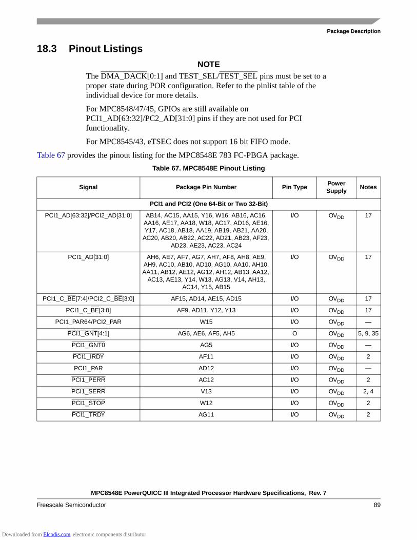
MPC8548E PowerQUICC III Integrated Processor Hardware Specifications, Rev. 7
Freescale Semiconductor 89
Package Description
18.3 Pinout ListingsNOTE
The DMA_DACK[0:1] and TEST_SEL/TEST_SEL pins must be set to a proper state during POR configuration. Refer to the pinlist table of the individual device for more details.
For MPC8548/47/45, GPIOs are still available on PCI1_AD[63:32]/PC2_AD[31:0] pins if they are not used for PCI functionality.
For MPC8545/43, eTSEC does not support 16 bit FIFO mode.
Table 67 provides the pinout listing for the MPC8548E 783 FC-PBGA package.Table 67. MPC8548E Pinout Listing
Signal Package Pin Number Pin TypePowerSupply
Notes
PCI1 and PCI2 (One 64-Bit or Two 32-Bit)
PCI1_AD[63:32]/PCI2_AD[31:0] AB14, AC15, AA15, Y16, W16, AB16, AC16, AA16, AE17, AA18, W18, AC17, AD16, AE16, Y17, AC18, AB18, AA19, AB19, AB21, AA20,
AC20, AB20, AB22, AC22, AD21, AB23, AF23, AD23, AE23, AC23, AC24
I/O OVDD 17
PCI1_AD[31:0] AH6, AE7, AF7, AG7, AH7, AF8, AH8, AE9, AH9, AC10, AB10, AD10, AG10, AA10, AH10, AA11, AB12, AE12, AG12, AH12, AB13, AA12,
AC13, AE13, Y14, W13, AG13, V14, AH13, AC14, Y15, AB15
I/O OVDD 17
PCI1_C_BE[7:4]/PCI2_C_BE[3:0] AF15, AD14, AE15, AD15 I/O OVDD 17
PCI1_C_BE[3:0] AF9, AD11, Y12, Y13 I/O OVDD 17
PCI1_PAR64/PCI2_PAR W15 I/O OVDD —
PCI1_GNT[4:1] AG6, AE6, AF5, AH5 O OVDD 5, 9, 35
PCI1_GNT0 AG5 I/O OVDD —
PCI1_IRDY AF11 I/O OVDD 2
PCI1_PAR AD12 I/O OVDD —
PCI1_PERR AC12 I/O OVDD 2
PCI1_SERR V13 I/O OVDD 2, 4
PCI1_STOP W12 I/O OVDD 2
PCI1_TRDY AG11 I/O OVDD 2
Downloaded from Elcodis.com electronic components distributor
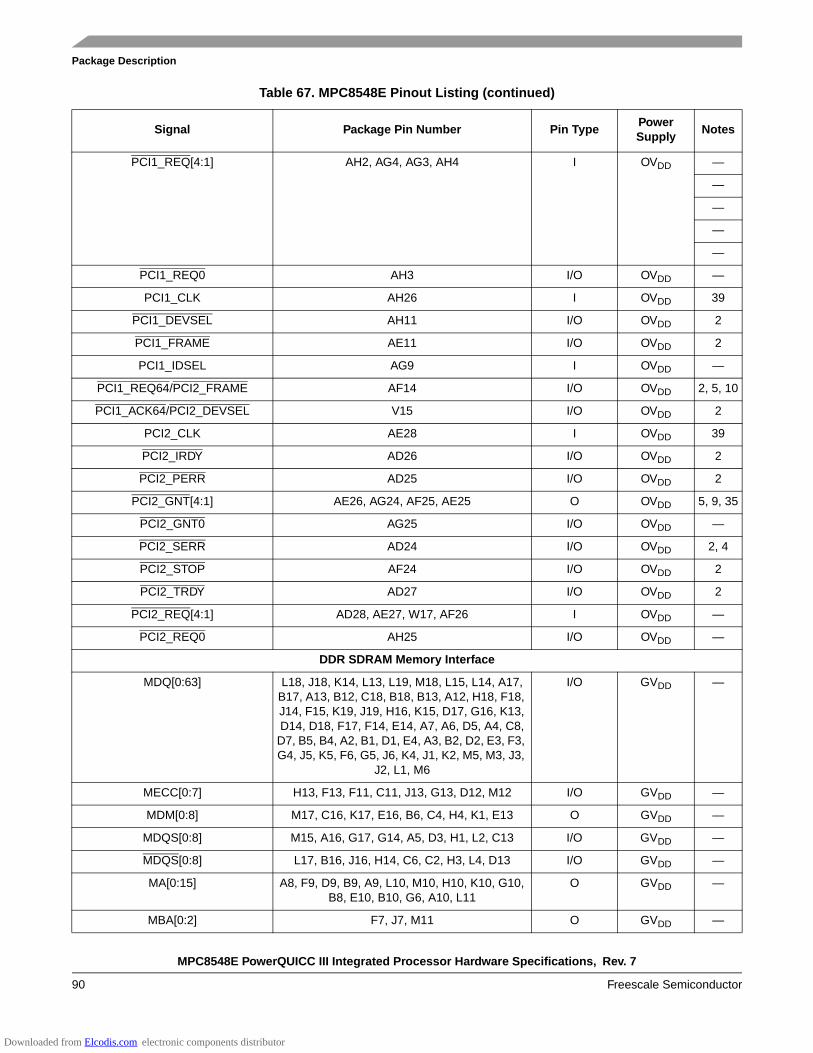
MPC8548E PowerQUICC III Integrated Processor Hardware Specifications, Rev. 7
90 Freescale Semiconductor
Package Description
PCI1_REQ[4:1] AH2, AG4, AG3, AH4 I OVDD —
—
—
—
—
PCI1_REQ0 AH3 I/O OVDD —
PCI1_CLK AH26 I OVDD 39
PCI1_DEVSEL AH11 I/O OVDD 2
PCI1_FRAME AE11 I/O OVDD 2
PCI1_IDSEL AG9 I OVDD —
PCI1_REQ64/PCI2_FRAME AF14 I/O OVDD 2, 5, 10
PCI1_ACK64/PCI2_DEVSEL V15 I/O OVDD 2
PCI2_CLK AE28 I OVDD 39
PCI2_IRDY AD26 I/O OVDD 2
PCI2_PERR AD25 I/O OVDD 2
PCI2_GNT[4:1] AE26, AG24, AF25, AE25 O OVDD 5, 9, 35
PCI2_GNT0 AG25 I/O OVDD —
PCI2_SERR AD24 I/O OVDD 2, 4
PCI2_STOP AF24 I/O OVDD 2
PCI2_TRDY AD27 I/O OVDD 2
PCI2_REQ[4:1] AD28, AE27, W17, AF26 I OVDD —
PCI2_REQ0 AH25 I/O OVDD —
DDR SDRAM Memory Interface
MDQ[0:63] L18, J18, K14, L13, L19, M18, L15, L14, A17, B17, A13, B12, C18, B18, B13, A12, H18, F18, J14, F15, K19, J19, H16, K15, D17, G16, K13, D14, D18, F17, F14, E14, A7, A6, D5, A4, C8,
D7, B5, B4, A2, B1, D1, E4, A3, B2, D2, E3, F3, G4, J5, K5, F6, G5, J6, K4, J1, K2, M5, M3, J3,
J2, L1, M6
I/O GVDD —
MECC[0:7] H13, F13, F11, C11, J13, G13, D12, M12 I/O GVDD —
MDM[0:8] M17, C16, K17, E16, B6, C4, H4, K1, E13 O GVDD —
MDQS[0:8] M15, A16, G17, G14, A5, D3, H1, L2, C13 I/O GVDD —
MDQS[0:8] L17, B16, J16, H14, C6, C2, H3, L4, D13 I/O GVDD —
MA[0:15] A8, F9, D9, B9, A9, L10, M10, H10, K10, G10, B8, E10, B10, G6, A10, L11
O GVDD —
MBA[0:2] F7, J7, M11 O GVDD —
Table 67. MPC8548E Pinout Listing (continued)
Signal Package Pin Number Pin TypePowerSupply
Notes
Downloaded from Elcodis.com electronic components distributor

MPC8548E PowerQUICC III Integrated Processor Hardware Specifications, Rev. 7
Freescale Semiconductor 91
Package Description
MWE E7 O GVDD —
MCAS H7 O GVDD —
MRAS L8 O GVDD —
MCKE[0:3] F10, C10, J11, H11 O GVDD 11
MCS[0:3] K8, J8, G8, F8 O GVDD —
MCK[0:5] H9, B15, G2, M9, A14, F1 O GVDD —
MCK[0:5] J9, A15, G1, L9, B14, F2 O GVDD —
MODT[0:3] E6, K6, L7, M7 O GVDD —
MDIC[0:1] A19, B19 I/O GVDD 36
Local Bus Controller Interface
LAD[0:31] E27, B20, H19, F25, A20, C19, E28, J23, A25, K22, B28, D27, D19, J22, K20, D28, D25, B25, E22, F22, F21, C25, C22, B23, F20, A23, A22,
E19, A21, D21, F19, B21
I/O BVDD —
LDP[0:3] K21, C28, B26, B22 I/O BVDD —
LA[27] H21 O BVDD 5, 9
LA[28:31] H20, A27, D26, A28 O BVDD 5, 7, 9
LCS[0:4] J25, C20, J24, G26, A26 O BVDD
LCS5/DMA_DREQ2 D23 I/O BVDD 1
LCS6/DMA_DACK2 G20 O BVDD 1
LCS7/DMA_DDONE2 E21 O BVDD 1
LWE0/LBS0/LSDDQM[0] G25 O BVDD 5, 9
LWE1/LBS1/LSDDQM[1] C23 O BVDD 5, 9
LWE2/LBS2/LSDDQM[2] J21 O BVDD 5, 9
LWE3/LBS3/LSDDQM[3] A24 O BVDD 5, 9
LALE H24 O BVDD 5, 8, 9
LBCTL G27 O BVDD 5, 8, 9
LGPL0/LSDA10 F23 O BVDD 5, 9
LGPL1/LSDWE G22 O BVDD 5, 9
LGPL2/LOE/LSDRAS B27 O BVDD 5, 8, 9
LGPL3/LSDCAS F24 O BVDD 5, 9
LGPL4/LGTA/LUPWAIT/LPBSE H23 I/O BVDD 114
LGPL5 E26 O BVDD 5, 9
LCKE E24 O BVDD —
LCLK[0:2] E23, D24, H22 O BVDD —
Table 67. MPC8548E Pinout Listing (continued)
Signal Package Pin Number Pin TypePowerSupply
Notes
Downloaded from Elcodis.com electronic components distributor
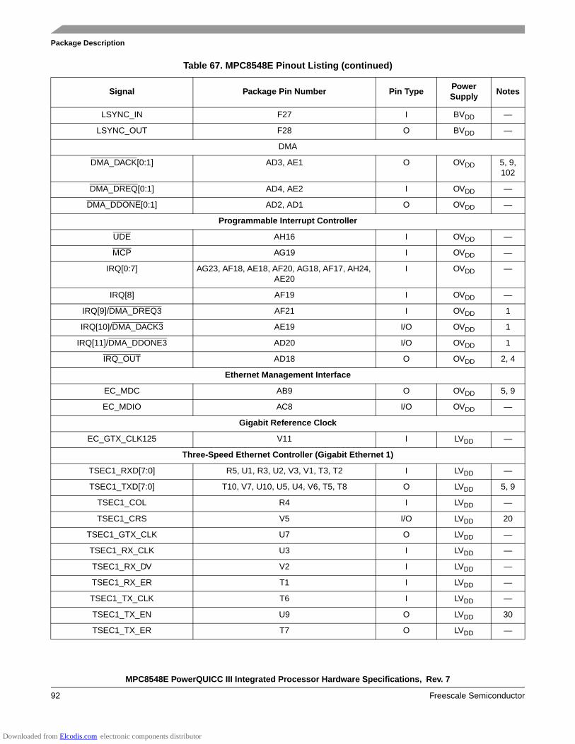
MPC8548E PowerQUICC III Integrated Processor Hardware Specifications, Rev. 7
92 Freescale Semiconductor
Package Description
LSYNC_IN F27 I BVDD —
LSYNC_OUT F28 O BVDD —
DMA
DMA_DACK[0:1] AD3, AE1 O OVDD 5, 9, 102
DMA_DREQ[0:1] AD4, AE2 I OVDD —
DMA_DDONE[0:1] AD2, AD1 O OVDD —
Programmable Interrupt Controller
UDE AH16 I OVDD —
MCP AG19 I OVDD —
IRQ[0:7] AG23, AF18, AE18, AF20, AG18, AF17, AH24, AE20
I OVDD —
IRQ[8] AF19 I OVDD —
IRQ[9]/DMA_DREQ3 AF21 I OVDD 1
IRQ[10]/DMA_DACK3 AE19 I/O OVDD 1
IRQ[11]/DMA_DDONE3 AD20 I/O OVDD 1
IRQ_OUT AD18 O OVDD 2, 4
Ethernet Management Interface
EC_MDC AB9 O OVDD 5, 9
EC_MDIO AC8 I/O OVDD —
Gigabit Reference Clock
EC_GTX_CLK125 V11 I LVDD —
Three-Speed Ethernet Controller (Gigabit Ethernet 1)
TSEC1_RXD[7:0] R5, U1, R3, U2, V3, V1, T3, T2 I LVDD —
TSEC1_TXD[7:0] T10, V7, U10, U5, U4, V6, T5, T8 O LVDD 5, 9
TSEC1_COL R4 I LVDD —
TSEC1_CRS V5 I/O LVDD 20
TSEC1_GTX_CLK U7 O LVDD —
TSEC1_RX_CLK U3 I LVDD —
TSEC1_RX_DV V2 I LVDD —
TSEC1_RX_ER T1 I LVDD —
TSEC1_TX_CLK T6 I LVDD —
TSEC1_TX_EN U9 O LVDD 30
TSEC1_TX_ER T7 O LVDD —
Table 67. MPC8548E Pinout Listing (continued)
Signal Package Pin Number Pin TypePowerSupply
Notes
Downloaded from Elcodis.com electronic components distributor

MPC8548E PowerQUICC III Integrated Processor Hardware Specifications, Rev. 7
Freescale Semiconductor 93
Package Description
Three-Speed Ethernet Controller (Gigabit Ethernet 2)
TSEC2_RXD[7:0] P2, R2, N1, N2, P3, M2, M1, N3 I LVDD —
TSEC2_TXD[7:0] N9, N10, P8, N7, R9, N5, R8, N6 O LVDD 5, 9, 33
TSEC2_COL P1 I LVDD —
TSEC2_CRS R6 I/O LVDD 20
TSEC2_GTX_CLK P6 O LVDD
TSEC2_RX_CLK N4 I LVDD —
TSEC2_RX_DV P5 I LVDD —
TSEC2_RX_ER R1 I LVDD —
TSEC2_TX_CLK P10 I LVDD —
TSEC2_TX_EN P7 O LVDD 30
TSEC2_TX_ER R10 O LVDD 5, 9, 33
Three-Speed Ethernet Controller (Gigabit Ethernet 3)
TSEC3_TXD[3:0] V8, W10, Y10, W7 O TVDD 5, 9, 29
TSEC3_RXD[3:0] Y1, W3, W5, W4 I TVDD —
TSEC3_GTX_CLK W8 O TVDD —
TSEC3_RX_CLK W2 I TVDD —
TSEC3_RX_DV W1 I TVDD —
TSEC3_RX_ER Y2 I TVDD —
TSEC3_TX_CLK V10 I TVDD —
TSEC3_TX_EN V9 O TVDD 30
Three-Speed Ethernet Controller (Gigabit Ethernet 4)
TSEC4_TXD[3:0]/TSEC3_TXD[7:4] AB8, Y7, AA7, Y8 O TVDD 1, 5, 9, 29
TSEC4_RXD[3:0]/TSEC3_RXD[7:4] AA1, Y3, AA2, AA4 I TVDD 1
TSEC4_GTX_CLK AA5 O TVDD —
TSEC4_RX_CLK/TSEC3_COL Y5 I TVDD 1
TSEC4_RX_DV/TSEC3_CRS AA3 I/O TVDD 1, 31
TSEC4_TX_EN/TSEC3_TX_ER AB6 O TVDD 1, 30
DUART
UART_CTS[0:1] AB3, AC5 I OVDD —
UART_RTS[0:1] AC6, AD7 O OVDD —
UART_SIN[0:1] AB5, AC7 I OVDD —
UART_SOUT[0:1] AB7, AD8 O OVDD —
Table 67. MPC8548E Pinout Listing (continued)
Signal Package Pin Number Pin TypePowerSupply
Notes
Downloaded from Elcodis.com electronic components distributor

MPC8548E PowerQUICC III Integrated Processor Hardware Specifications, Rev. 7
94 Freescale Semiconductor
Package Description
I2C interface
IIC1_SCL AG22 I/O OVDD 4, 27
IIC1_SDA AG21 I/O OVDD 4, 27
IIC2_SCL AG15 I/O OVDD 4, 27
IIC2_SDA AG14 I/O OVDD 4, 27
SerDes
SD_RX[0:7] M28, N26, P28, R26, W26, Y28, AA26, AB28 I XVDD —
SD_RX[0:7] M27, N25, P27, R25, W25, Y27, AA25, AB27 I XVDD —
SD_TX[0:7] M22, N20, P22, R20, U20, V22, W20, Y22 O XVDD —
SD_TX[0:7] M23, N21, P23, R21, U21, V23, W21, Y23 O XVDD —
SD_PLL_TPD U28 O XVDD 24
SD_REF_CLK T28 I XVDD 3
SD_REF_CLK T27 I XVDD 3
Reserved AC1, AC3 — — 2
Reserved M26, V28 — — 32
Reserved M25, V27 — — 34
Reserved M20, M21, T22, T23 — — 38
General-Purpose Output
GPOUT[24:31] K26, K25, H27, G28, H25, J26, K24, K23 O BVDD —
System Control
HRESET AG17 I OVDD —
HRESET_REQ AG16 O OVDD 29
SRESET AG20 I OVDD —
CKSTP_IN AA9 I OVDD —
CKSTP_OUT AA8 O OVDD 2, 4
Debug
TRIG_IN AB2 I OVDD —
TRIG_OUT/READY/QUIESCE AB1 O OVDD 6, 9, 19, 29
MSRCID[0:1] AE4, AG2 O OVDD 5, 6, 9
MSRCID[2:4] AF3, AF1, AF2 O OVDD 6, 19, 29
MDVAL AE5 O OVDD 6
CLK_OUT AE21 O OVDD 11
Table 67. MPC8548E Pinout Listing (continued)
Signal Package Pin Number Pin TypePowerSupply
Notes
Downloaded from Elcodis.com electronic components distributor
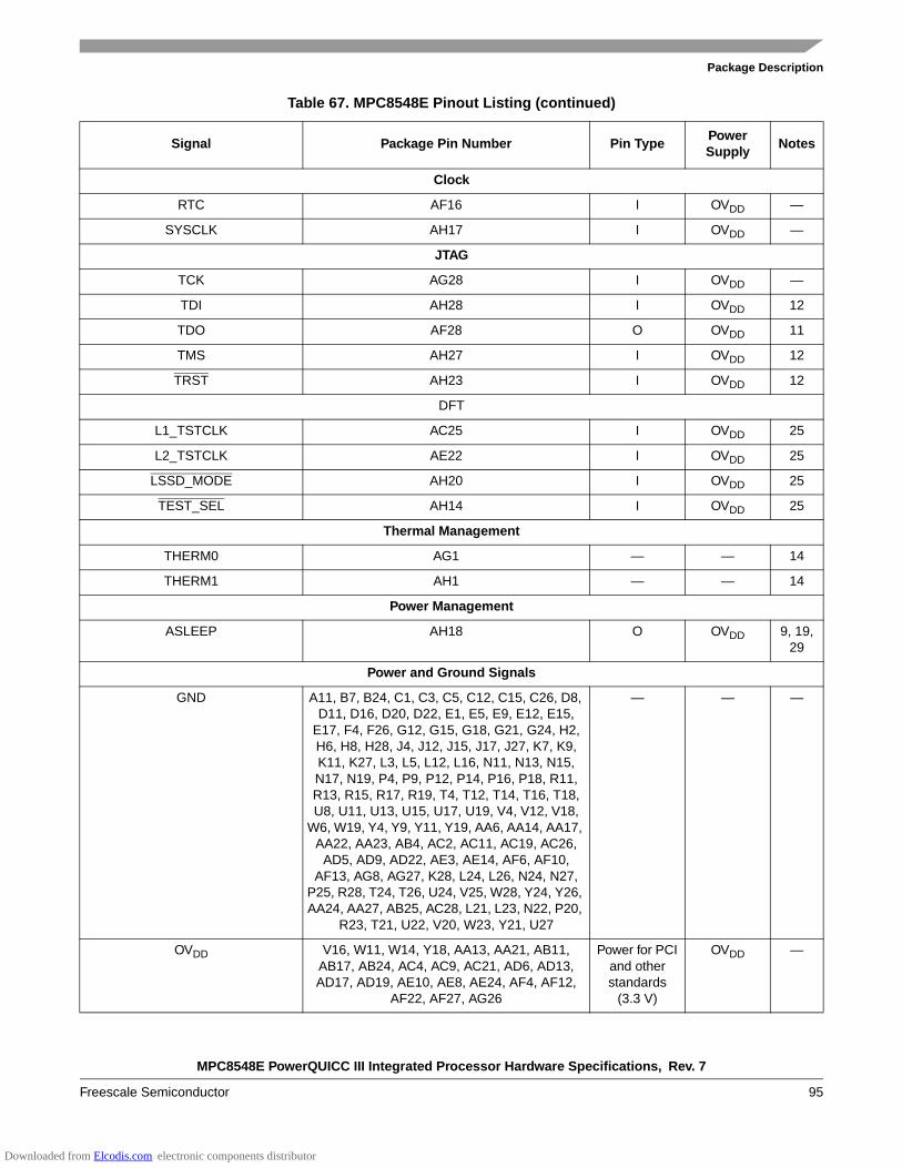
MPC8548E PowerQUICC III Integrated Processor Hardware Specifications, Rev. 7
Freescale Semiconductor 95
Package Description
Clock
RTC AF16 I OVDD —
SYSCLK AH17 I OVDD —
JTAG
TCK AG28 I OVDD —
TDI AH28 I OVDD 12
TDO AF28 O OVDD 11
TMS AH27 I OVDD 12
TRST AH23 I OVDD 12
DFT
L1_TSTCLK AC25 I OVDD 25
L2_TSTCLK AE22 I OVDD 25
LSSD_MODE AH20 I OVDD 25
TEST_SEL AH14 I OVDD 25
Thermal Management
THERM0 AG1 — — 14
THERM1 AH1 — — 14
Power Management
ASLEEP AH18 O OVDD 9, 19, 29
Power and Ground Signals
GND A11, B7, B24, C1, C3, C5, C12, C15, C26, D8, D11, D16, D20, D22, E1, E5, E9, E12, E15,
E17, F4, F26, G12, G15, G18, G21, G24, H2, H6, H8, H28, J4, J12, J15, J17, J27, K7, K9, K11, K27, L3, L5, L12, L16, N11, N13, N15, N17, N19, P4, P9, P12, P14, P16, P18, R11, R13, R15, R17, R19, T4, T12, T14, T16, T18, U8, U11, U13, U15, U17, U19, V4, V12, V18,
W6, W19, Y4, Y9, Y11, Y19, AA6, AA14, AA17, AA22, AA23, AB4, AC2, AC11, AC19, AC26,
AD5, AD9, AD22, AE3, AE14, AF6, AF10, AF13, AG8, AG27, K28, L24, L26, N24, N27,
P25, R28, T24, T26, U24, V25, W28, Y24, Y26, AA24, AA27, AB25, AC28, L21, L23, N22, P20,
R23, T21, U22, V20, W23, Y21, U27
— — —
OVDD V16, W11, W14, Y18, AA13, AA21, AB11, AB17, AB24, AC4, AC9, AC21, AD6, AD13, AD17, AD19, AE10, AE8, AE24, AF4, AF12,
AF22, AF27, AG26
Power for PCI and other standards
(3.3 V)
OVDD —
Table 67. MPC8548E Pinout Listing (continued)
Signal Package Pin Number Pin TypePowerSupply
Notes
Downloaded from Elcodis.com electronic components distributor

MPC8548E PowerQUICC III Integrated Processor Hardware Specifications, Rev. 7
96 Freescale Semiconductor
Package Description
LVDD N8, R7, T9, U6 Power for TSEC1 and
TSEC2(2.5 V, 3.3 V)
LVDD —
TVDD W9, Y6 Power for TSEC3 and
TSEC4(2,5 V, 3.3 V)
TVDD —
GVDD B3, B11, C7, C9, C14, C17, D4, D6, D10, D15, E2, E8, E11, E18, F5, F12, F16, G3, G7, G9, G11, H5, H12, H15, H17, J10, K3, K12, K16,
K18, L6, M4, M8, M13
Power for DDR1 and
DDR2 DRAM I/O voltage (1.8 V, 2.5)
GVDD —
BVDD C21, C24, C27, E20, E25, G19, G23, H26, J20 Power for local bus (1.8 V,
2.5 V, 3.3 V)
BVDD —
VDD M19, N12, N14, N16, N18, P11, P13, P15, P17, P19, R12, R14, R16, R18, T11, T13, T15, T17,
T19, U12, U14, U16, U18, V17, V19
Power for core (1.1 V)
VDD —
SVDD L25, L27, M24, N28, P24, P26, R24, R27, T25, V24, V26, W24, W27, Y25, AA28, AC27
Core Power for SerDes
transceivers(1.1 V)
SVDD —
XVDD L20, L22, N23, P21, R22, T20, U23, V21, W22, Y20
Pad Power for SerDes
transceivers(1.1 V)
XVDD —
AVDD_LBIU J28 Power for local bus PLL(1.1 V)
— 26
AVDD_PCI1 AH21 Power for PCI1 PLL
(1.1 V)
— 26
AVDD_PCI2 AH22 Power for PCI2 PLL
(1.1 V)
— 26
AVDD_CORE AH15 Power for e500 PLL (1.1 V)
— 26
AVDD_PLAT AH19 Power for CCB PLL (1.1 V)
— 26
AVDD_SRDS U25 Power for SRDSPLL
(1.1 V)
— 26
SENSEVDD M14 O VDD 13
SENSEVSS M16 — — 13
Table 67. MPC8548E Pinout Listing (continued)
Signal Package Pin Number Pin TypePowerSupply
Notes
Downloaded from Elcodis.com electronic components distributor

MPC8548E PowerQUICC III Integrated Processor Hardware Specifications, Rev. 7
Freescale Semiconductor 97
Package Description
Analog Signals
MVREF A18 IReference
voltage signal for DDR
MVREF —
SD_IMP_CAL_RX L28 I 200Ω to GND
—
SD_IMP_CAL_TX AB26 I 100Ω to GND
—
SD_PLL_TPA U26 O — 24
Notes:1. All multiplexed signals are listed only once and do not re-occur. For example, LCS5/DMA_REQ2 is listed only once in the
local bus controller section, and is not mentioned in the DMA section even though the pin also functions as DMA_REQ2.2. Recommend a weak pull-up resistor (2–10 kΩ) be placed on this pin to OVDD.3. A valid clock must be provided at POR if TSEC4_TXD[2] is set = 1.4. This pin is an open drain signal.5. This pin is a reset configuration pin. It has a weak internal pull-up P-FET which is enabled only when the processor is in the
reset state. This pull-up is designed such that it can be overpowered by an external 4.7-kΩ pull-down resistor. However, if the signal is intended to be high after reset, and if there is any device on the net which might pull down the value of the net at reset, then a pullup or active driver is needed.
6. Treat these pins as no connects (NC) unless using debug address functionality.7. The value of LA[28:31] during reset sets the CCB clock to SYSCLK PLL ratio. These pins require 4.7-kΩ pull-up or pull-down
resistors. See Section 19.2, “CCB/SYSCLK PLL Ratio.” 8. The value of LALE, LGPL2, and LBCTL at reset set the e500 core clock to CCB clock PLL ratio. These pins require 4.7-kΩ
pull-up or pull-down resistors. See the Section 19.3, “e500 Core PLL Ratio.”9. Functionally, this pin is an output, but structurally it is an I/O because it either samples configuration input during reset or
because it has other manufacturing test functions. This pin therefore is described as an I/O for boundary scan.10.This pin functionally requires a pull-up resistor, but during reset it is a configuration input that controls 32- vs. 64-bit PCI
operation. Therefore, it must be actively driven low during reset by reset logic if the device is to be configured to be a 64-bit PCI device. Refer to the PCI Specification.
11.This output is actively driven during reset rather than being three-stated during reset.12.These JTAG pins have weak internal pull-up P-FETs that are always enabled.13.These pins are connected to the VDD/GND planes internally and may be used by the core power supply to improve tracking
and regulation.14.Internal thermally sensitive resistor.15.No connections should be made to these pins if they are not used.16.These pins are not connected for any use.17.PCI specifications recommend that a weak pull-up resistor (2–10 kΩ) be placed on the higher order pins to OVDD when using
64-bit buffer mode (pins PCI_AD[63:32] and PCI1_C_BE[7:4]). 19.If this pin is connected to a device that pulls down during reset, an external pull-up is required to drive this pin to a safe state
during reset.20.This pin is only an output in FIFO mode when used as Rx flow control.24.Do not connect.
Table 67. MPC8548E Pinout Listing (continued)
Signal Package Pin Number Pin TypePowerSupply
Notes
Downloaded from Elcodis.com electronic components distributor

MPC8548E PowerQUICC III Integrated Processor Hardware Specifications, Rev. 7
98 Freescale Semiconductor
Package Description
25.These are test signals for factory use only and must be pulled up (100 Ω–1 kΩ) to OVDD for normal machine operation.26.Independent supplies derived from board VDD.27.Recommend a pull-up resistor (~1 kW) be placed on this pin to OVDD.29. The following pins must NOT be pulled down during power-on reset: TSEC3_TXD[3], TSEC4_TXD3/TSEC3_TXD7,
HRESET_REQ, TRIG_OUT/READY/QUIESCE, MSRCID[2:4], ASLEEP. 30.This pin requires an external 4.7-kΩ pull-down resistor to prevent PHY from seeing a valid transmit enable before it is actively
driven.31.This pin is only an output in eTSEC3 FIFO mode when used as Rx flow control.32.These pins should be connected to XVDD.33.TSEC2_TXD1, TSEC2_TX_ER are multiplexed as cfg_dram_type[0:1]. They must be valid at power-up, even before
HRESET assertion.34.These pins should be pulled to ground through a 300-Ω (±10%) resistor.35.When a PCI block is disabled, either the POR config pin that selects between internal and external arbiter must be pulled
down to select external arbiter if there is any other PCI device connected on the PCI bus, or leave the PCIn_AD pins as ‘no connect’ or terminated through 2–10 kΩ pull-up resistors with the default of internal arbiter if the PCIn_AD pins are not connected to any other PCI device. The PCI block drives the PCIn_AD pins if it is configured to be the PCI arbiter—through POR config pins—irrespective of whether it is disabled via the DEVDISR register or not. It may cause contention if there is any other PCI device connected on the bus.
36.MDIC0 is grounded through an 18.2-Ω precision 1% resistor and MDIC1 is connected to GVDD through an 18.2-Ω precision 1% resistor. These pins are used for automatic calibration of the DDR IOs.
38.These pins should be left floating.39. If PCI1 or PCI2 is configured as PCI asynchronous mode, a valid clock must be provided on pin PCI1_CLK or PCI2_CLK.
Otherwise the processor will not boot up.40.These pins should be connected to GND.101.This pin requires an external 4.7-kΩ resistor to GND.102.For Rev. 2.x silicon, DMA_DACK[0:1] must be 0b11 during POR configuration; for rev. 1.x silicon, the pin values during POR
configuration are don’t care.103.If these pins are not used as GPINn (general-purpose input), they should be pulled low (to GND) or high (to LVDD) through
2–10 kΩ resistors.104.These should be pulled low to GND through 2–10 kΩ resistors if they are not used.105.These should be pulled low or high to LVDD through 2–10 kΩ resistors if they are not used.106.For rev. 2.x silicon, DMA_DACK[0:1] must be 0b10 during POR configuration; for rev. 1.x silicon, the pin values during POR
configuration are don’t care.107.For rev. 2.x silicon, DMA_DACK[0:1] must be 0b01 during POR configuration; for rev. 1.x silicon, the pin values during POR
configuration are don’t care.108.For rev. 2.x silicon, DMA_DACK[0:1] must be 0b11 during POR configuration; for rev. 1.x silicon, the pin values during POR
configuration are don’t care.109.This is a test signal for factory use only and must be pulled down (100 Ω – 1 kΩ) to GND for normal machine operation.110.These pins should be pulled high to OVDD through 2–10 kΩ resistors.111.If these pins are not used as GPINn (general-purpose input), they should be pulled low (to GND) or high (to OVDD) through
2–10 kΩ resistors.112.This pin must not be pulled down during POR configuration.113.These should be pulled low or high to OVDD through 2–10 kΩ resistors.114.For systems that boot from local bus (GPCM)-controlled flash, a pullup on LGPL4 is required.
Table 67. MPC8548E Pinout Listing (continued)
Signal Package Pin Number Pin TypePowerSupply
Notes
Downloaded from Elcodis.com electronic components distributor

MPC8548E PowerQUICC III Integrated Processor Hardware Specifications, Rev. 7
Freescale Semiconductor 99
Package Description
Table 68 provides the pin-out listing for the MPC8547E 783 FC-PBGA package.
NOTEAll note references in the following table use the same numbers as those for Table 67. Refer to Table 67 for the meanings of these notes.
Table 68. MPC8547E Pinout Listing
Signal Package Pin Number Pin TypePowerSupply
Notes
PCI1 (One 64-Bit or One 32-Bit)
PCI1_AD[63:32] AB14, AC15, AA15, Y16, W16, AB16, AC16, AA16, AE17, AA18, W18, AC17, AD16, AE16, Y17, AC18, AB18, AA19, AB19, AB21, AA20,
AC20, AB20, AB22, AC22, AD21, AB23, AF23, AD23, AE23, AC23, AC24
I/O OVDD 17
PCI1_AD[31:0] AH6, AE7, AF7, AG7, AH7, AF8, AH8, AE9, AH9, AC10, AB10, AD10, AG10, AA10, AH10, AA11, AB12, AE12, AG12, AH12, AB13, AA12,
AC13, AE13, Y14, W13, AG13, V14, AH13, AC14, Y15, AB15
I/O OVDD 17
PCI1_C_BE[7:4] AF15, AD14, AE15, AD15 I/O OVDD 17
PCI1_C_BE[3:0] AF9, AD11, Y12, Y13 I/O OVDD 17
PCI1_PAR64 W15 I/O OVDD —
PCI1_GNT[4:1] AG6, AE6, AF5, AH5 O OVDD 5, 9, 35
PCI1_GNT0 AG5 I/O OVDD —
PCI1_IRDY AF11 I/O OVDD 2
PCI1_PAR AD12 I/O OVDD —
PCI1_PERR AC12 I/O OVDD 2
PCI1_SERR V13 I/O OVDD 2, 4
PCI1_STOP W12 I/O OVDD 2
PCI1_TRDY AG11 I/O OVDD 2
PCI1_REQ[4:1] AH2, AG4, AG3, AH4 I OVDD —
PCI1_REQ0 AH3 I/O OVDD —
PCI1_CLK AH26 I OVDD 39
PCI1_DEVSEL AH11 I/O OVDD 2
PCI1_FRAME AE11 I/O OVDD 2
PCI1_IDSEL AG9 I OVDD —
PCI1_REQ64 AF14 I/O OVDD 2, 5,10
PCI1_ACK64 V15 I/O OVDD 2
Reserved AE28 — — 2
Reserved AD26 — — 2
Reserved AD25 — — 2
Downloaded from Elcodis.com electronic components distributor

MPC8548E PowerQUICC III Integrated Processor Hardware Specifications, Rev. 7
100 Freescale Semiconductor
Package Description
Reserved AE26 — — 2
cfg_pci1_clk AG24 I OVDD 5
Reserved AF25 — — 101
Reserved AE25 — — 2
Reserved AG25 — — 2
Reserved AD24 — — 2
Reserved AF24 — — 2
Reserved AD27 — — 2
Reserved AD28, AE27, W17, AF26 — — 2
Reserved AH25 — — 2
DDR SDRAM Memory Interface
MDQ[0:63] L18, J18, K14, L13, L19, M18, L15, L14, A17, B17, A13, B12, C18, B18, B13, A12, H18, F18, J14, F15, K19, J19, H16, K15, D17, G16, K13, D14, D18, F17, F14, E14, A7, A6, D5, A4, C8,
D7, B5, B4, A2, B1, D1, E4, A3, B2, D2, E3, F3, G4, J5, K5, F6, G5, J6, K4, J1, K2, M5, M3, J3,
J2, L1, M6
I/O GVDD —
MECC[0:7] H13, F13, F11, C11, J13, G13, D12, M12 I/O GVDD —
MDM[0:8] M17, C16, K17, E16, B6, C4, H4, K1, E13 O GVDD —
MDQS[0:8] M15, A16, G17, G14, A5, D3, H1, L2, C13 I/O GVDD —
MDQS[0:8] L17, B16, J16, H14, C6, C2, H3, L4, D13 I/O GVDD —
MA[0:15] A8, F9, D9, B9, A9, L10, M10, H10, K10, G10, B8, E10, B10, G6, A10, L11
O GVDD —
MBA[0:2] F7, J7, M11 O GVDD —
MWE E7 O GVDD —
MCAS H7 O GVDD —
MRAS L8 O GVDD —
MCKE[0:3] F10, C10, J11, H11 O GVDD 11
MCS[0:3] K8, J8, G8, F8 O GVDD —
MCK[0:5] H9, B15, G2, M9, A14, F1 O GVDD —
MCK[0:5] J9, A15, G1, L9, B14, F2 O GVDD —
MODT[0:3] E6, K6, L7, M7 O GVDD —
MDIC[0:1] A19, B19 I/O GVDD 36
Table 68. MPC8547E Pinout Listing (continued)
Signal Package Pin Number Pin TypePowerSupply
Notes
Downloaded from Elcodis.com electronic components distributor

MPC8548E PowerQUICC III Integrated Processor Hardware Specifications, Rev. 7
Freescale Semiconductor 101
Package Description
Local Bus Controller Interface
LAD[0:31] E27, B20, H19, F25, A20, C19, E28, J23, A25, K22, B28, D27, D19, J22, K20, D28, D25, B25, E22, F22, F21, C25, C22, B23, F20, A23, A22,
E19, A21, D21, F19, B21
I/O BVDD —
LDP[0:3] K21, C28, B26, B22 I/O BVDD —
LA[27] H21 O BVDD 5, 9
LA[28:31] H20, A27, D26, A28 O BVDD 5, 7, 9
LCS[0:4] J25, C20, J24, G26, A26 O BVDD —
LCS5/DMA_DREQ2 D23 I/O BVDD 1
LCS6/DMA_DACK2 G20 O BVDD 1
LCS7/DMA_DDONE2 E21 O BVDD 1
LWE0/LBS0/LSDDQM[0] G25 O BVDD 5, 9
LWE1/LBS1/LSDDQM[1] C23 O BVDD 5, 9
LWE2/LBS2/LSDDQM[2] J21 O BVDD 5, 9
LWE3/LBS3/LSDDQM[3] A24 O BVDD 5, 9
LALE H24 O BVDD 5, 8, 9
LBCTL G27 O BVDD 5, 8, 9
LGPL0/LSDA10 F23 O BVDD 5, 9
LGPL1/LSDWE G22 O BVDD 5, 9
LGPL2/LOE/LSDRAS B27 O BVDD 5, 8, 9
LGPL3/LSDCAS F24 O BVDD 5, 9
LGPL4/LGTA/LUPWAIT/LPBSE H23 I/O BVDD 114
LGPL5 E26 O BVDD 5, 9
LCKE E24 O BVDD —
LCLK[0:2] E23, D24, H22 O BVDD —
LSYNC_IN F27 I BVDD —
LSYNC_OUT F28 O BVDD —
DMA
DMA_DACK[0:1] AD3, AE1 O OVDD 5, 9, 107
DMA_DREQ[0:1] AD4, AE2 I OVDD —
DMA_DDONE[0:1] AD2, AD1 O OVDD —
Programmable Interrupt Controller
UDE AH16 I OVDD —
MCP AG19 I OVDD —
Table 68. MPC8547E Pinout Listing (continued)
Signal Package Pin Number Pin TypePowerSupply
Notes
Downloaded from Elcodis.com electronic components distributor

MPC8548E PowerQUICC III Integrated Processor Hardware Specifications, Rev. 7
102 Freescale Semiconductor
Package Description
IRQ[0:7] AG23, AF18, AE18, AF20, AG18, AF17, AH24, AE20
I OVDD —
IRQ[8] AF19 I OVDD —
IRQ[9]/DMA_DREQ3 AF21 I OVDD 1
IRQ[10]/DMA_DACK3 AE19 I/O OVDD 1
IRQ[11]/DMA_DDONE3 AD20 I/O OVDD 1
IRQ_OUT AD18 O OVDD 2, 4
Ethernet Management Interface
EC_MDC AB9 O OVDD 5, 9
EC_MDIO AC8 I/O OVDD —
Gigabit Reference Clock
EC_GTX_CLK125 V11 I LVDD —
Three-Speed Ethernet Controller (Gigabit Ethernet 1)
TSEC1_RXD[7:0] R5, U1, R3, U2, V3, V1, T3, T2 I LVDD —
TSEC1_TXD[7:0] T10, V7, U10, U5, U4, V6, T5, T8 O LVDD 5, 9
TSEC1_COL R4 I LVDD —
TSEC1_CRS V5 I/O LVDD 20
TSEC1_GTX_CLK U7 O LVDD —
TSEC1_RX_CLK U3 I LVDD —
TSEC1_RX_DV V2 I LVDD —
TSEC1_RX_ER T1 I LVDD —
TSEC1_TX_CLK T6 I LVDD —
TSEC1_TX_EN U9 O LVDD 30
TSEC1_TX_ER T7 O LVDD —
Three-Speed Ethernet Controller (Gigabit Ethernet 2)
TSEC2_RXD[7:0] P2, R2, N1, N2, P3, M2, M1, N3 I LVDD —
TSEC2_TXD[7:0] N9, N10, P8, N7, R9, N5, R8, N6 O LVDD 5, 9, 33
TSEC2_COL P1 I LVDD —
TSEC2_CRS R6 I/O LVDD 20
TSEC2_GTX_CLK P6 O LVDD —
TSEC2_RX_CLK N4 I LVDD —
TSEC2_RX_DV P5 I LVDD —
TSEC2_RX_ER R1 I LVDD —
TSEC2_TX_CLK P10 I LVDD —
TSEC2_TX_EN P7 O LVDD 30
Table 68. MPC8547E Pinout Listing (continued)
Signal Package Pin Number Pin TypePowerSupply
Notes
Downloaded from Elcodis.com electronic components distributor
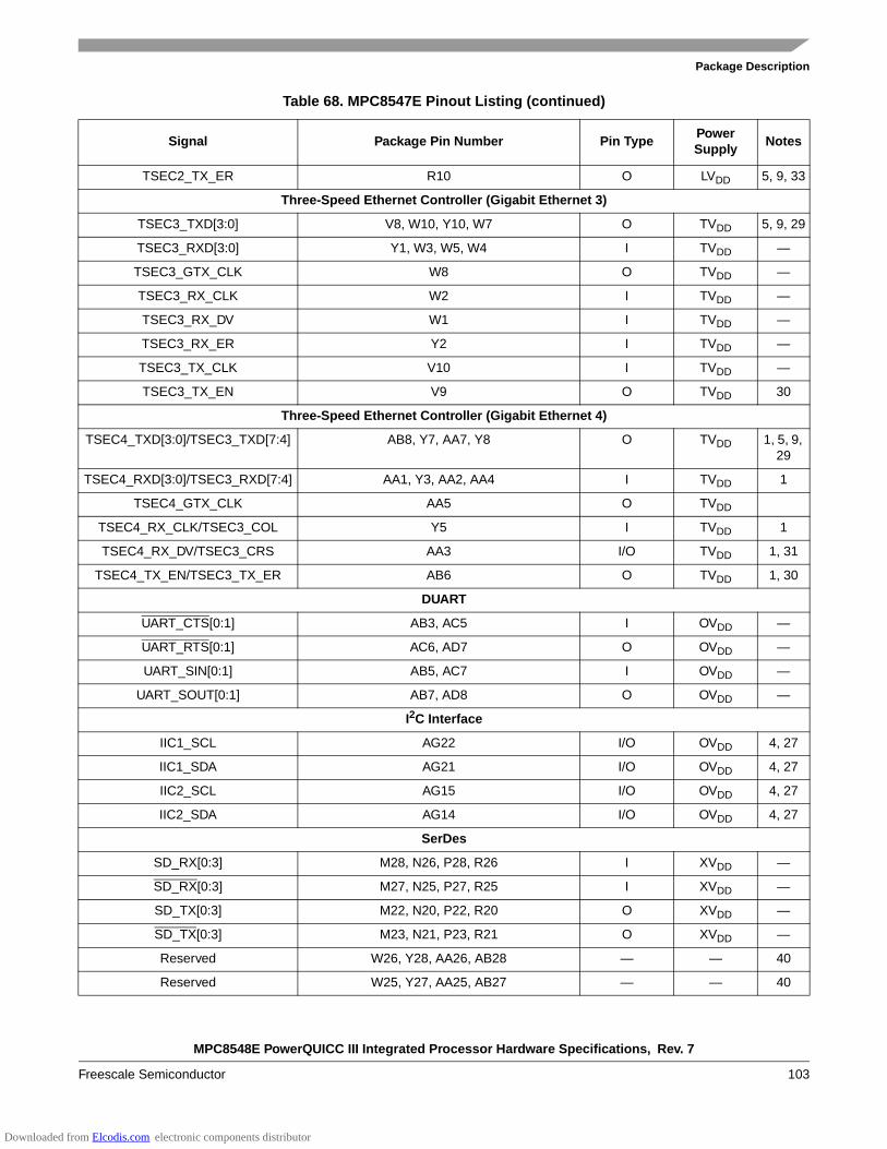
MPC8548E PowerQUICC III Integrated Processor Hardware Specifications, Rev. 7
Freescale Semiconductor 103
Package Description
TSEC2_TX_ER R10 O LVDD 5, 9, 33
Three-Speed Ethernet Controller (Gigabit Ethernet 3)
TSEC3_TXD[3:0] V8, W10, Y10, W7 O TVDD 5, 9, 29
TSEC3_RXD[3:0] Y1, W3, W5, W4 I TVDD —
TSEC3_GTX_CLK W8 O TVDD —
TSEC3_RX_CLK W2 I TVDD —
TSEC3_RX_DV W1 I TVDD —
TSEC3_RX_ER Y2 I TVDD —
TSEC3_TX_CLK V10 I TVDD —
TSEC3_TX_EN V9 O TVDD 30
Three-Speed Ethernet Controller (Gigabit Ethernet 4)
TSEC4_TXD[3:0]/TSEC3_TXD[7:4] AB8, Y7, AA7, Y8 O TVDD 1, 5, 9, 29
TSEC4_RXD[3:0]/TSEC3_RXD[7:4] AA1, Y3, AA2, AA4 I TVDD 1
TSEC4_GTX_CLK AA5 O TVDD
TSEC4_RX_CLK/TSEC3_COL Y5 I TVDD 1
TSEC4_RX_DV/TSEC3_CRS AA3 I/O TVDD 1, 31
TSEC4_TX_EN/TSEC3_TX_ER AB6 O TVDD 1, 30
DUART
UART_CTS[0:1] AB3, AC5 I OVDD —
UART_RTS[0:1] AC6, AD7 O OVDD —
UART_SIN[0:1] AB5, AC7 I OVDD —
UART_SOUT[0:1] AB7, AD8 O OVDD —
I2C Interface
IIC1_SCL AG22 I/O OVDD 4, 27
IIC1_SDA AG21 I/O OVDD 4, 27
IIC2_SCL AG15 I/O OVDD 4, 27
IIC2_SDA AG14 I/O OVDD 4, 27
SerDes
SD_RX[0:3] M28, N26, P28, R26 I XVDD —
SD_RX[0:3] M27, N25, P27, R25 I XVDD —
SD_TX[0:3] M22, N20, P22, R20 O XVDD —
SD_TX[0:3] M23, N21, P23, R21 O XVDD —
Reserved W26, Y28, AA26, AB28 — — 40
Reserved W25, Y27, AA25, AB27 — — 40
Table 68. MPC8547E Pinout Listing (continued)
Signal Package Pin Number Pin TypePowerSupply
Notes
Downloaded from Elcodis.com electronic components distributor
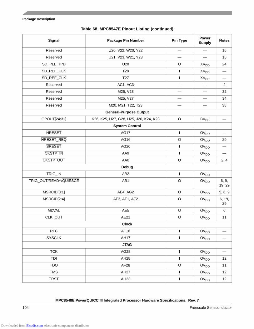
MPC8548E PowerQUICC III Integrated Processor Hardware Specifications, Rev. 7
104 Freescale Semiconductor
Package Description
Reserved U20, V22, W20, Y22 — — 15
Reserved U21, V23, W21, Y23 — — 15
SD_PLL_TPD U28 O XVDD 24
SD_REF_CLK T28 I XVDD —
SD_REF_CLK T27 I XVDD —
Reserved AC1, AC3 — — 2
Reserved M26, V28 — — 32
Reserved M25, V27 — — 34
Reserved M20, M21, T22, T23 — — 38
General-Purpose Output
GPOUT[24:31] K26, K25, H27, G28, H25, J26, K24, K23 O BVDD —
System Control
HRESET AG17 I OVDD —
HRESET_REQ AG16 O OVDD 29
SRESET AG20 I OVDD —
CKSTP_IN AA9 I OVDD —
CKSTP_OUT AA8 O OVDD 2, 4
Debug
TRIG_IN AB2 I OVDD —
TRIG_OUT/READY/QUIESCE AB1 O OVDD 6, 9, 19, 29
MSRCID[0:1] AE4, AG2 O OVDD 5, 6, 9
MSRCID[2:4] AF3, AF1, AF2 O OVDD 6, 19, 29
MDVAL AE5 O OVDD 6
CLK_OUT AE21 O OVDD 11
Clock
RTC AF16 I OVDD —
SYSCLK AH17 I OVDD —
JTAG
TCK AG28 I OVDD —
TDI AH28 I OVDD 12
TDO AF28 O OVDD 11
TMS AH27 I OVDD 12
TRST AH23 I OVDD 12
Table 68. MPC8547E Pinout Listing (continued)
Signal Package Pin Number Pin TypePowerSupply
Notes
Downloaded from Elcodis.com electronic components distributor

MPC8548E PowerQUICC III Integrated Processor Hardware Specifications, Rev. 7
Freescale Semiconductor 105
Package Description
DFT
L1_TSTCLK AC25 I OVDD 25
L2_TSTCLK AE22 I OVDD 25
LSSD_MODE AH20 I OVDD 25
TEST_SEL AH14 I OVDD 25
Thermal Management
THERM0 AG1 — — 14
THERM1 AH1 — — 14
Power Management
ASLEEP AH18 O OVDD 9, 19, 29
Power and Ground Signals
GND A11, B7, B24, C1, C3, C5, C12, C15, C26, D8, D11, D16, D20, D22, E1, E5, E9, E12, E15,
E17, F4, F26, G12, G15, G18, G21, G24, H2, H6, H8, H28, J4, J12, J15, J17, J27, K7, K9, K11, K27, L3, L5, L12, L16, N11, N13, N15, N17, N19, P4, P9, P12, P14, P16, P18, R11, R13, R15, R17, R19, T4, T12, T14, T16, T18, U8, U11, U13, U15, U17, U19, V4, V12, V18,
W6, W19, Y4, Y9, Y11, Y19, AA6, AA14, AA17, AA22, AA23, AB4, AC2, AC11, AC19, AC26,
AD5, AD9, AD22, AE3, AE14, AF6, AF10, AF13, AG8, AG27, K28, L24, L26, N24, N27,
P25, R28, T24, T26, U24, V25, W28, Y24, Y26, AA24, AA27, AB25, AC28, L21, L23, N22, P20,
R23, T21, U22, V20, W23, Y21, U27
— — —
OVDD V16, W11, W14, Y18, AA13, AA21, AB11, AB17, AB24, AC4, AC9, AC21, AD6, AD13, AD17, AD19, AE10, AE8, AE24, AF4, AF12,
AF22, AF27, AG26
Power for PCI and other standards
(3.3 V)
OVDD —
LVDD N8, R7, T9, U6 Power for TSEC1 and
TSEC2(2.5 V, 3.3 V)
LVDD —
TVDD W9, Y6 Power for TSEC3 and
TSEC4(2,5 V, 3.3 V)
TVDD —
GVDD B3, B11, C7, C9, C14, C17, D4, D6, D10, D15, E2, E8, E11, E18, F5, F12, F16, G3, G7, G9, G11, H5, H12, H15, H17, J10, K3, K12, K16,
K18, L6, M4, M8, M13
Power for DDR1 and
DDR2 DRAM I/O voltage
(1.8 V, 2.5 V)
GVDD —
Table 68. MPC8547E Pinout Listing (continued)
Signal Package Pin Number Pin TypePowerSupply
Notes
Downloaded from Elcodis.com electronic components distributor

MPC8548E PowerQUICC III Integrated Processor Hardware Specifications, Rev. 7
106 Freescale Semiconductor
Package Description
BVDD C21, C24, C27, E20, E25, G19, G23, H26, J20 Power for local bus (1.8 V,
2.5 V, 3.3 V)
BVDD —
VDD M19, N12, N14, N16, N18, P11, P13, P15, P17, P19, R12, R14, R16, R18, T11, T13, T15, T17,
T19, U12, U14, U16, U18, V17, V19
Power for core (1.1 V)
VDD —
SVDD L25, L27, M24, N28, P24, P26, R24, R27, T25, V24, V26, W24, W27, Y25, AA28, AC27
Core power for SerDes
transceivers(1.1 V)
SVDD —
XVDD L20, L22, N23, P21, R22, T20, U23, V21, W22, Y20
Pad Power for SerDes
transceivers(1.1 V)
XVDD —
AVDD_LBIU J28 Power for local bus PLL(1.1 V)
— 26
AVDD_PCI1 AH21 Power for PCI1 PLL
(1.1 V)
— 26
AVDD_PCI2 AH22 Power for PCI2 PLL
(1.1 V)
— 26
AVDD_CORE AH15 Power for e500 PLL (1.1 V)
— 26
AVDD_PLAT AH19 Power for CCB PLL (1.1 V)
— 26
AVDD_SRDS U25 Power for SRDSPLL
(1.1 V)
— 26
SENSEVDD M14 O VDD 13
SENSEVSS M16 — — 13
Analog Signals
MVREF A18 IReference
voltage signal for DDR
MVREF —
SD_IMP_CAL_RX L28 I 200 Ω to GND
—
SD_IMP_CAL_TX AB26 I 100 Ω to GND
—
SD_PLL_TPA U26 O — 24
Note: All note references in this table use the same numbers as those for Table 67. Refer to Table 67 for the meanings of these notes.
Table 68. MPC8547E Pinout Listing (continued)
Signal Package Pin Number Pin TypePowerSupply
Notes
Downloaded from Elcodis.com electronic components distributor
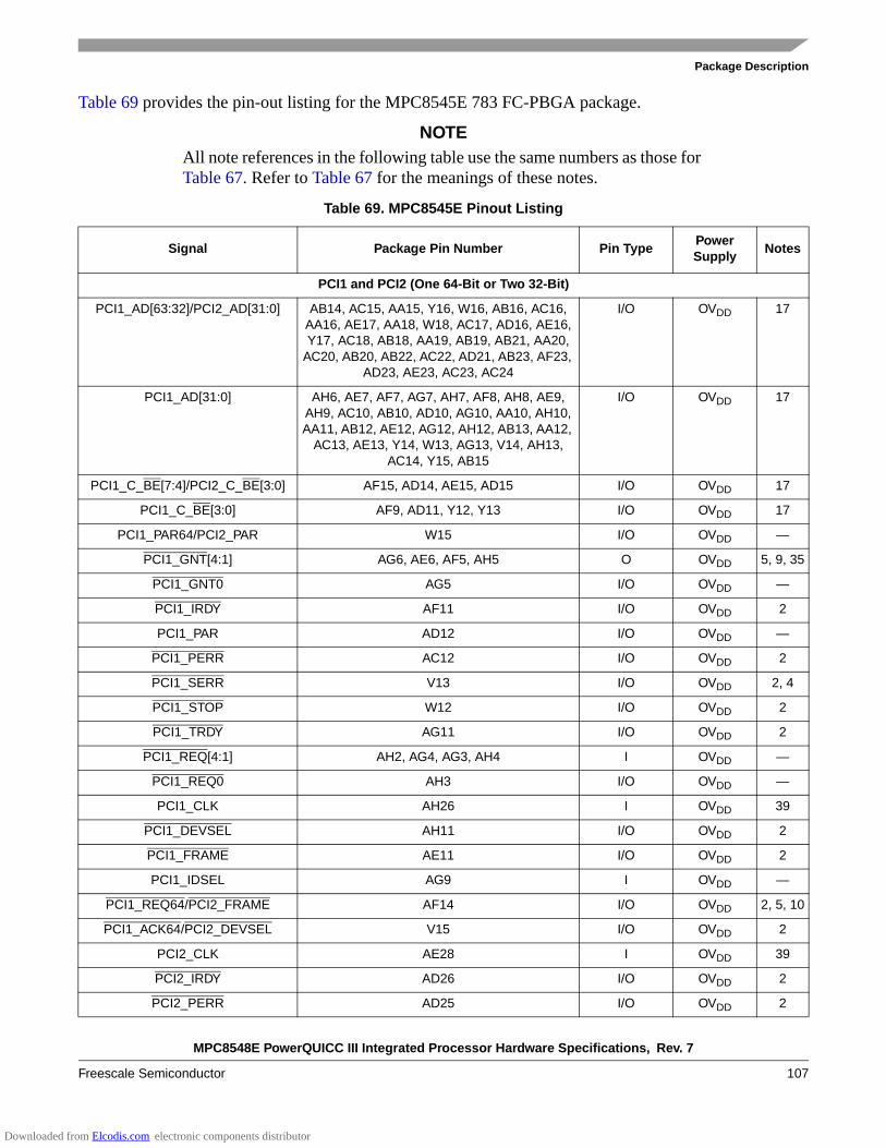
MPC8548E PowerQUICC III Integrated Processor Hardware Specifications, Rev. 7
Freescale Semiconductor 107
Package Description
Table 69 provides the pin-out listing for the MPC8545E 783 FC-PBGA package.
NOTEAll note references in the following table use the same numbers as those for Table 67. Refer to Table 67 for the meanings of these notes.
Table 69. MPC8545E Pinout Listing
Signal Package Pin Number Pin TypePowerSupply
Notes
PCI1 and PCI2 (One 64-Bit or Two 32-Bit)
PCI1_AD[63:32]/PCI2_AD[31:0] AB14, AC15, AA15, Y16, W16, AB16, AC16, AA16, AE17, AA18, W18, AC17, AD16, AE16, Y17, AC18, AB18, AA19, AB19, AB21, AA20,
AC20, AB20, AB22, AC22, AD21, AB23, AF23, AD23, AE23, AC23, AC24
I/O OVDD 17
PCI1_AD[31:0] AH6, AE7, AF7, AG7, AH7, AF8, AH8, AE9, AH9, AC10, AB10, AD10, AG10, AA10, AH10, AA11, AB12, AE12, AG12, AH12, AB13, AA12,
AC13, AE13, Y14, W13, AG13, V14, AH13, AC14, Y15, AB15
I/O OVDD 17
PCI1_C_BE[7:4]/PCI2_C_BE[3:0] AF15, AD14, AE15, AD15 I/O OVDD 17
PCI1_C_BE[3:0] AF9, AD11, Y12, Y13 I/O OVDD 17
PCI1_PAR64/PCI2_PAR W15 I/O OVDD —
PCI1_GNT[4:1] AG6, AE6, AF5, AH5 O OVDD 5, 9, 35
PCI1_GNT0 AG5 I/O OVDD —
PCI1_IRDY AF11 I/O OVDD 2
PCI1_PAR AD12 I/O OVDD —
PCI1_PERR AC12 I/O OVDD 2
PCI1_SERR V13 I/O OVDD 2, 4
PCI1_STOP W12 I/O OVDD 2
PCI1_TRDY AG11 I/O OVDD 2
PCI1_REQ[4:1] AH2, AG4, AG3, AH4 I OVDD —
PCI1_REQ0 AH3 I/O OVDD —
PCI1_CLK AH26 I OVDD 39
PCI1_DEVSEL AH11 I/O OVDD 2
PCI1_FRAME AE11 I/O OVDD 2
PCI1_IDSEL AG9 I OVDD —
PCI1_REQ64/PCI2_FRAME AF14 I/O OVDD 2, 5, 10
PCI1_ACK64/PCI2_DEVSEL V15 I/O OVDD 2
PCI2_CLK AE28 I OVDD 39
PCI2_IRDY AD26 I/O OVDD 2
PCI2_PERR AD25 I/O OVDD 2
Downloaded from Elcodis.com electronic components distributor
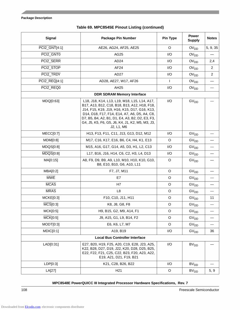
MPC8548E PowerQUICC III Integrated Processor Hardware Specifications, Rev. 7
108 Freescale Semiconductor
Package Description
PCI2_GNT[4:1] AE26, AG24, AF25, AE25 O OVDD 5, 9, 35
PCI2_GNT0 AG25 I/O OVDD —
PCI2_SERR AD24 I/O OVDD 2,4
PCI2_STOP AF24 I/O OVDD 2
PCI2_TRDY AD27 I/O OVDD 2
PCI2_REQ[4:1] AD28, AE27, W17, AF26 I OVDD —
PCI2_REQ0 AH25 I/O OVDD —
DDR SDRAM Memory Interface
MDQ[0:63] L18, J18, K14, L13, L19, M18, L15, L14, A17, B17, A13, B12, C18, B18, B13, A12, H18, F18, J14, F15, K19, J19, H16, K15, D17, G16, K13, D14, D18, F17, F14, E14, A7, A6, D5, A4, C8,
D7, B5, B4, A2, B1, D1, E4, A3, B2, D2, E3, F3, G4, J5, K5, F6, G5, J6, K4, J1, K2, M5, M3, J3,
J2, L1, M6
I/O GVDD —
MECC[0:7] H13, F13, F11, C11, J13, G13, D12, M12 I/O GVDD —
MDM[0:8] M17, C16, K17, E16, B6, C4, H4, K1, E13 O GVDD —
MDQS[0:8] M15, A16, G17, G14, A5, D3, H1, L2, C13 I/O GVDD —
MDQS[0:8] L17, B16, J16, H14, C6, C2, H3, L4, D13 I/O GVDD —
MA[0:15] A8, F9, D9, B9, A9, L10, M10, H10, K10, G10, B8, E10, B10, G6, A10, L11
O GVDD —
MBA[0:2] F7, J7, M11 O GVDD —
MWE E7 O GVDD —
MCAS H7 O GVDD —
MRAS L8 O GVDD —
MCKE[0:3] F10, C10, J11, H11 O GVDD 11
MCS[0:3] K8, J8, G8, F8 O GVDD —
MCK[0:5] H9, B15, G2, M9, A14, F1 O GVDD —
MCK[0:5] J9, A15, G1, L9, B14, F2 O GVDD —
MODT[0:3] E6, K6, L7, M7 O GVDD —
MDIC[0:1] A19, B19 I/O GVDD 36
Local Bus Controller Interface
LAD[0:31] E27, B20, H19, F25, A20, C19, E28, J23, A25, K22, B28, D27, D19, J22, K20, D28, D25, B25, E22, F22, F21, C25, C22, B23, F20, A23, A22,
E19, A21, D21, F19, B21
I/O BVDD —
LDP[0:3] K21, C28, B26, B22 I/O BVDD —
LA[27] H21 O BVDD 5, 9
Table 69. MPC8545E Pinout Listing (continued)
Signal Package Pin Number Pin TypePowerSupply
Notes
Downloaded from Elcodis.com electronic components distributor

MPC8548E PowerQUICC III Integrated Processor Hardware Specifications, Rev. 7
Freescale Semiconductor 109
Package Description
LA[28:31] H20, A27, D26, A28 O BVDD 5, 7, 9
LCS[0:4] J25, C20, J24, G26, A26 O BVDD —
LCS5/DMA_DREQ2 D23 I/O BVDD 1
LCS6/DMA_DACK2 G20 O BVDD 1
LCS7/DMA_DDONE2 E21 O BVDD 1
LWE0/LBS0/LSDDQM[0] G25 O BVDD 5, 9
LWE1/LBS1/LSDDQM[1] C23 O BVDD 5, 9
LWE2/LBS2/LSDDQM[2] J21 O BVDD 5, 9
LWE3/LBS3/LSDDQM[3] A24 O BVDD 5, 9
LALE H24 O BVDD 5, 8, 9
LBCTL G27 O BVDD 5, 8, 9
LGPL0/LSDA10 F23 O BVDD 5, 9
LGPL1/LSDWE G22 O BVDD 5, 9
LGPL2/LOE/LSDRAS B27 O BVDD 5, 8, 9
LGPL3/LSDCAS F24 O BVDD 5, 9
LGPL4/LGTA/LUPWAIT/LPBSE H23 I/O BVDD 114
LGPL5 E26 O BVDD 5, 9
LCKE E24 O BVDD —
LCLK[0:2] E23, D24, H22 O BVDD —
LSYNC_IN F27 I BVDD —
LSYNC_OUT F28 O BVDD —
DMA
DMA_DACK[0:1] AD3, AE1 O OVDD 5, 9, 106
DMA_DREQ[0:1] AD4, AE2 I OVDD —
DMA_DDONE[0:1] AD2, AD1 O OVDD —
Programmable Interrupt Controller
UDE AH16 I OVDD —
MCP AG19 I OVDD —
IRQ[0:7] AG23, AF18, AE18, AF20, AG18, AF17, AH24, AE20
I OVDD —
IRQ[8] AF19 I OVDD —
IRQ[9]/DMA_DREQ3 AF21 I OVDD 1
IRQ[10]/DMA_DACK3 AE19 I/O OVDD 1
IRQ[11]/DMA_DDONE3 AD20 I/O OVDD 1
Table 69. MPC8545E Pinout Listing (continued)
Signal Package Pin Number Pin TypePowerSupply
Notes
Downloaded from Elcodis.com electronic components distributor

MPC8548E PowerQUICC III Integrated Processor Hardware Specifications, Rev. 7
110 Freescale Semiconductor
Package Description
IRQ_OUT AD18 O OVDD 2, 4
Ethernet Management Interface
EC_MDC AB9 O OVDD 5, 9
EC_MDIO AC8 I/O OVDD —
Gigabit Reference Clock
EC_GTX_CLK125 V11 I LVDD —
Three-Speed Ethernet Controller (Gigabit Ethernet 1)
TSEC1_RXD[7:0] R5, U1, R3, U2, V3, V1, T3, T2 I LVDD —
TSEC1_TXD[7:0] T10, V7, U10, U5, U4, V6, T5, T8 O LVDD 5, 9
TSEC1_COL R4 I LVDD —
TSEC1_CRS V5 I/O LVDD 20
TSEC1_GTX_CLK U7 O LVDD —
TSEC1_RX_CLK U3 I LVDD —
TSEC1_RX_DV V2 I LVDD —
TSEC1_RX_ER T1 I LVDD —
TSEC1_TX_CLK T6 I LVDD —
TSEC1_TX_EN U9 O LVDD 30
TSEC1_TX_ER T7 O LVDD —
GPIN[0:7] P2, R2, N1, N2, P3, M2, M1, N3 I LVDD 103
GPOUT[0:5] N9, N10, P8, N7, R9, N5 O LVDD —
cfg_dram_type0/GPOUT6 R8 O LVDD 5, 9
GPOUT7 N6 O LVDD —
Reserved P1 — — 104
Reserved R6 — — 104
Reserved P6 — — 15
Reserved N4 — — 105
FIFO1_RXC2 P5 I LVDD 104
Reserved R1 — — 104
Reserved P10 — — 105
FIFO1_TXC2 P7 O LVDD 15
cfg_dram_type1 R10 I LVDD 5
Three-Speed Ethernet Controller (Gigabit Ethernet 3)
TSEC3_TXD[3:0] V8, W10, Y10, W7 O TVDD 5, 9, 29
TSEC3_RXD[3:0] Y1, W3, W5, W4 I TVDD —
Table 69. MPC8545E Pinout Listing (continued)
Signal Package Pin Number Pin TypePowerSupply
Notes
Downloaded from Elcodis.com electronic components distributor

MPC8548E PowerQUICC III Integrated Processor Hardware Specifications, Rev. 7
Freescale Semiconductor 111
Package Description
TSEC3_GTX_CLK W8 O TVDD —
TSEC3_RX_CLK W2 I TVDD —
TSEC3_RX_DV W1 I TVDD —
TSEC3_RX_ER Y2 I TVDD —
TSEC3_TX_CLK V10 I TVDD —
TSEC3_TX_EN V9 O TVDD 30
TSEC3_TXD[7:4] AB8, Y7, AA7, Y8 O TVDD 5, 9, 29
TSEC3_RXD[7:4] AA1, Y3, AA2, AA4 I TVDD —
Reserved AA5 — — 15
TSEC3_COL Y5 I TVDD —
TSEC3_CRS AA3 I/O TVDD 31
TSEC3_TX_ER AB6 O TVDD —
DUART
UART_CTS[0:1] AB3, AC5 I OVDD —
UART_RTS[0:1] AC6, AD7 O OVDD —
UART_SIN[0:1] AB5, AC7 I OVDD —
UART_SOUT[0:1] AB7, AD8 O OVDD —
I2C interface
IIC1_SCL AG22 I/O OVDD 4, 27
IIC1_SDA AG21 I/O OVDD 4, 27
IIC2_SCL AG15 I/O OVDD 4, 27
IIC2_SDA AG14 I/O OVDD 4, 27
SerDes
SD_RX[0:3] M28, N26, P28, R26 I XVDD —
SD_RX[0:3] M27, N25, P27, R25 I XVDD —
SD_TX[0:3] M22, N20, P22, R20 O XVDD —
SD_TX[0:3] M23, N21, P23, R21 O XVDD —
Reserved W26, Y28, AA26, AB28 — — 40
Reserved W25, Y27, AA25, AB27 — — 40
Reserved U20, V22, W20, Y22 — — 15
Reserved U21, V23, W21, Y23 — — 15
SD_PLL_TPD U28 O XVDD 24
SD_REF_CLK T28 I XVDD —
SD_REF_CLK T27 I XVDD —
Table 69. MPC8545E Pinout Listing (continued)
Signal Package Pin Number Pin TypePowerSupply
Notes
Downloaded from Elcodis.com electronic components distributor

MPC8548E PowerQUICC III Integrated Processor Hardware Specifications, Rev. 7
112 Freescale Semiconductor
Package Description
Reserved AC1, AC3 — — 2
Reserved M26, V28 — — 32
Reserved M25, V27 — — 34
Reserved M20, M21, T22, T23 — — 38
General-Purpose Output
GPOUT[24:31] K26, K25, H27, G28, H25, J26, K24, K23 O BVDD —
System Control
HRESET AG17 I OVDD —
HRESET_REQ AG16 O OVDD 29
SRESET AG20 I OVDD —
CKSTP_IN AA9 I OVDD —
CKSTP_OUT AA8 O OVDD 2, 4
Debug
TRIG_IN AB2 I OVDD —
TRIG_OUT/READY/QUIESCE AB1 O OVDD 6, 9, 19, 29
MSRCID[0:1] AE4, AG2 O OVDD 5, 6, 9
MSRCID[2:4] AF3, AF1, AF2 O OVDD 6, 19, 29
MDVAL AE5 O OVDD 6
CLK_OUT AE21 O OVDD 11
Clock
RTC AF16 I OVDD —
SYSCLK AH17 I OVDD —
JTAG
TCK AG28 I OVDD —
TDI AH28 I OVDD 12
TDO AF28 O OVDD 11
TMS AH27 I OVDD 12
TRST AH23 I OVDD 12
DFT
L1_TSTCLK AC25 I OVDD 25
L2_TSTCLK AE22 I OVDD 25
LSSD_MODE AH20 I OVDD 25
TEST_SEL AH14 I OVDD 25
Table 69. MPC8545E Pinout Listing (continued)
Signal Package Pin Number Pin TypePowerSupply
Notes
Downloaded from Elcodis.com electronic components distributor

MPC8548E PowerQUICC III Integrated Processor Hardware Specifications, Rev. 7
Freescale Semiconductor 113
Package Description
Thermal Management
THERM0 AG1 — — 14
THERM1 AH1 — — 14
Power Management
ASLEEP AH18 O OVDD 9, 19, 29
Power and Ground Signals
GND A11, B7, B24, C1, C3, C5, C12, C15, C26, D8, D11, D16, D20, D22, E1, E5, E9, E12, E15,
E17, F4, F26, G12, G15, G18, G21, G24, H2, H6, H8, H28, J4, J12, J15, J17, J27, K7, K9, K11, K27, L3, L5, L12, L16, N11, N13, N15, N17, N19, P4, P9, P12, P14, P16, P18, R11, R13, R15, R17, R19, T4, T12, T14, T16, T18, U8, U11, U13, U15, U17, U19, V4, V12, V18,
W6, W19, Y4, Y9, Y11, Y19, AA6, AA14, AA17, AA22, AA23, AB4, AC2, AC11, AC19, AC26,
AD5, AD9, AD22, AE3, AE14, AF6, AF10, AF13, AG8, AG27, K28, L24, L26, N24, N27,
P25, R28, T24, T26, U24, V25, W28, Y24, Y26, AA24, AA27, AB25, AC28, L21, L23, N22, P20,
R23, T21, U22, V20, W23, Y21, U27
— — —
OVDD V16, W11, W14, Y18, AA13, AA21, AB11, AB17, AB24, AC4, AC9, AC21, AD6, AD13, AD17, AD19, AE10, AE8, AE24, AF4, AF12,
AF22, AF27, AG26
Power for PCI and other standards
(3.3 V)
OVDD —
LVDD N8, R7, T9, U6 Power for TSEC1 and
TSEC2(2.5 V, 3.3 V)
LVDD —
TVDD W9, Y6 Power for TSEC3 and
TSEC4(2,5 V, 3.3 V)
TVDD —
GVDD B3, B11, C7, C9, C14, C17, D4, D6, D10, D15, E2, E8, E11, E18, F5, F12, F16, G3, G7, G9, G11, H5, H12, H15, H17, J10, K3, K12, K16,
K18, L6, M4, M8, M13
Power for DDR1 and
DDR2 DRAM I/O voltage
(1.8 V, 2.5 V)
GVDD —
BVDD C21, C24, C27, E20, E25, G19, G23, H26, J20 Power for local bus (1.8 V,
2.5 V, 3.3 V)
BVDD —
VDD M19, N12, N14, N16, N18, P11, P13, P15, P17, P19, R12, R14, R16, R18, T11, T13, T15, T17,
T19, U12, U14, U16, U18, V17, V19
Power for core (1.1 V)
VDD —
Table 69. MPC8545E Pinout Listing (continued)
Signal Package Pin Number Pin TypePowerSupply
Notes
Downloaded from Elcodis.com electronic components distributor

MPC8548E PowerQUICC III Integrated Processor Hardware Specifications, Rev. 7
114 Freescale Semiconductor
Package Description
SVDD L25, L27, M24, N28, P24, P26, R24, R27, T25, V24, V26, W24, W27, Y25, AA28, AC27
Core power for SerDes
transceivers(1.1 V)
SVDD —
XVDD L20, L22, N23, P21, R22, T20, U23, V21, W22, Y20
Pad power for SerDes
transceivers(1.1 V)
XVDD —
AVDD_LBIU J28 Power for local bus PLL(1.1 V)
— 26
AVDD_PCI1 AH21 Power for PCI1 PLL
(1.1 V)
— 26
AVDD_PCI2 AH22 Power for PCI2 PLL
(1.1 V)
— 26
AVDD_CORE AH15 Power for e500 PLL (1.1 V)
— 26
AVDD_PLAT AH19 Power for CCB PLL (1.1 V)
— 26
AVDD_SRDS U25 Power for SRDSPLL (1.1
V)
— 26
SENSEVDD M14 O VDD 13
SENSEVSS M16 — — 13
Analog Signals
MVREF A18 IReference
voltage signal for DDR
MVREF —
SD_IMP_CAL_RX L28 I 200 Ω to GND
—
SD_IMP_CAL_TX AB26 I 100 Ω to GND
—
SD_PLL_TPA U26 O — 24
Note: All note references in this table use the same numbers as those for Table 67. Refer to Table 67 for the meanings of these notes.
Table 69. MPC8545E Pinout Listing (continued)
Signal Package Pin Number Pin TypePowerSupply
Notes
Downloaded from Elcodis.com electronic components distributor
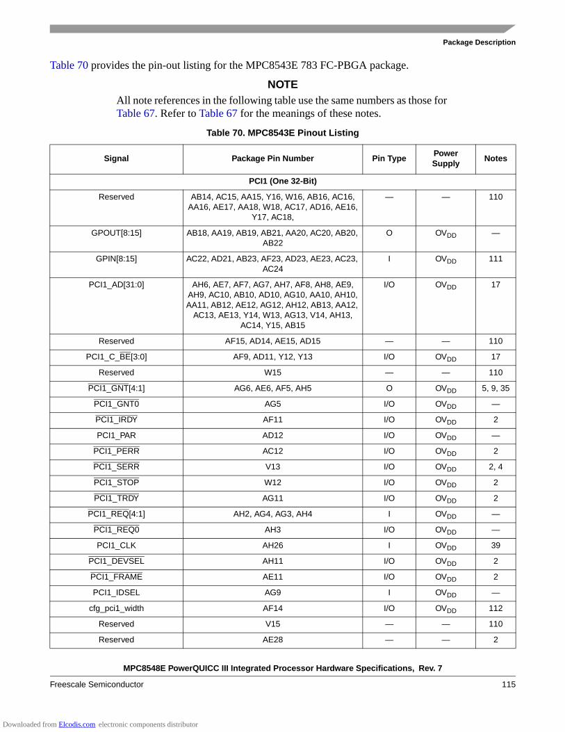
MPC8548E PowerQUICC III Integrated Processor Hardware Specifications, Rev. 7
Freescale Semiconductor 115
Package Description
Table 70 provides the pin-out listing for the MPC8543E 783 FC-PBGA package.
NOTEAll note references in the following table use the same numbers as those for Table 67. Refer to Table 67 for the meanings of these notes.
Table 70. MPC8543E Pinout Listing
Signal Package Pin Number Pin TypePowerSupply
Notes
PCI1 (One 32-Bit)
Reserved AB14, AC15, AA15, Y16, W16, AB16, AC16, AA16, AE17, AA18, W18, AC17, AD16, AE16,
Y17, AC18,
— — 110
GPOUT[8:15] AB18, AA19, AB19, AB21, AA20, AC20, AB20, AB22
O OVDD —
GPIN[8:15] AC22, AD21, AB23, AF23, AD23, AE23, AC23, AC24
I OVDD 111
PCI1_AD[31:0] AH6, AE7, AF7, AG7, AH7, AF8, AH8, AE9, AH9, AC10, AB10, AD10, AG10, AA10, AH10, AA11, AB12, AE12, AG12, AH12, AB13, AA12,
AC13, AE13, Y14, W13, AG13, V14, AH13, AC14, Y15, AB15
I/O OVDD 17
Reserved AF15, AD14, AE15, AD15 — — 110
PCI1_C_BE[3:0] AF9, AD11, Y12, Y13 I/O OVDD 17
Reserved W15 — — 110
PCI1_GNT[4:1] AG6, AE6, AF5, AH5 O OVDD 5, 9, 35
PCI1_GNT0 AG5 I/O OVDD —
PCI1_IRDY AF11 I/O OVDD 2
PCI1_PAR AD12 I/O OVDD —
PCI1_PERR AC12 I/O OVDD 2
PCI1_SERR V13 I/O OVDD 2, 4
PCI1_STOP W12 I/O OVDD 2
PCI1_TRDY AG11 I/O OVDD 2
PCI1_REQ[4:1] AH2, AG4, AG3, AH4 I OVDD —
PCI1_REQ0 AH3 I/O OVDD —
PCI1_CLK AH26 I OVDD 39
PCI1_DEVSEL AH11 I/O OVDD 2
PCI1_FRAME AE11 I/O OVDD 2
PCI1_IDSEL AG9 I OVDD —
cfg_pci1_width AF14 I/O OVDD 112
Reserved V15 — — 110
Reserved AE28 — — 2
Downloaded from Elcodis.com electronic components distributor

MPC8548E PowerQUICC III Integrated Processor Hardware Specifications, Rev. 7
116 Freescale Semiconductor
Package Description
Reserved AD26 — — 110
Reserved AD25 — — 110
Reserved AE26 — — 110
cfg_pci1_clk AG24 I OVDD 5
Reserved AF25 — — 101
Reserved AE25 — — 110
Reserved AG25 — — 110
Reserved AD24 — — 110
Reserved AF24 — — 110
Reserved AD27 — — 110
Reserved AD28, AE27, W17, AF26 — — 110
Reserved AH25 — — 110
DDR SDRAM Memory Interface
MDQ[0:63] L18, J18, K14, L13, L19, M18, L15, L14, A17, B17, A13, B12, C18, B18, B13, A12, H18, F18, J14, F15, K19, J19, H16, K15, D17, G16, K13, D14, D18, F17, F14, E14, A7, A6, D5, A4, C8,
D7, B5, B4, A2, B1, D1, E4, A3, B2, D2, E3, F3, G4, J5, K5, F6, G5, J6, K4, J1, K2, M5, M3, J3,
J2, L1, M6
I/O GVDD —
MECC[0:7] H13, F13, F11, C11, J13, G13, D12, M12 I/O GVDD —
MDM[0:8] M17, C16, K17, E16, B6, C4, H4, K1, E13 O GVDD —
MDQS[0:8] M15, A16, G17, G14, A5, D3, H1, L2, C13 I/O GVDD —
MDQS[0:8] L17, B16, J16, H14, C6, C2, H3, L4, D13 I/O GVDD —
MA[0:15] A8, F9, D9, B9, A9, L10, M10, H10, K10, G10, B8, E10, B10, G6, A10, L11
O GVDD —
MBA[0:2] F7, J7, M11 O GVDD —
MWE E7 O GVDD —
MCAS H7 O GVDD —
MRAS L8 O GVDD —
MCKE[0:3] F10, C10, J11, H11 O GVDD 11
MCS[0:3] K8, J8, G8, F8 O GVDD —
MCK[0:5] H9, B15, G2, M9, A14, F1 O GVDD —
MCK[0:5] J9, A15, G1, L9, B14, F2 O GVDD —
MODT[0:3] E6, K6, L7, M7 O GVDD —
MDIC[0:1] A19, B19 I/O GVDD 36
Local Bus Controller Interface
Table 70. MPC8543E Pinout Listing (continued)
Signal Package Pin Number Pin TypePowerSupply
Notes
Downloaded from Elcodis.com electronic components distributor

MPC8548E PowerQUICC III Integrated Processor Hardware Specifications, Rev. 7
Freescale Semiconductor 117
Package Description
LAD[0:31] E27, B20, H19, F25, A20, C19, E28, J23, A25, K22, B28, D27, D19, J22, K20, D28, D25, B25, E22, F22, F21, C25, C22, B23, F20, A23, A22,
E19, A21, D21, F19, B21
I/O BVDD —
LDP[0:3] K21, C28, B26, B22 I/O BVDD —
LA[27] H21 O BVDD 5, 9
LA[28:31] H20, A27, D26, A28 O BVDD 5, 7, 9
LCS[0:4] J25, C20, J24, G26, A26 O BVDD —
LCS5/DMA_DREQ2 D23 I/O BVDD 1
LCS6/DMA_DACK2 G20 O BVDD 1
LCS7/DMA_DDONE2 E21 O BVDD 1
LWE0/LBS0/LSDDQM[0] G25 O BVDD 5, 9
LWE1/LBS1/LSDDQM[1] C23 O BVDD 5, 9
LWE2/LBS2/LSDDQM[2] J21 O BVDD 5, 9
LWE3/LBS3/LSDDQM[3] A24 O BVDD 5, 9
LALE H24 O BVDD 5, 8, 9
LBCTL G27 O BVDD 5, 8, 9
LGPL0/LSDA10 F23 O BVDD 5, 9
LGPL1/LSDWE G22 O BVDD 5, 9
LGPL2/LOE/LSDRAS B27 O BVDD 5, 8, 9
LGPL3/LSDCAS F24 O BVDD 5, 9
LGPL4/LGTA/LUPWAIT/LPBSE H23 I/O BVDD 114
LGPL5 E26 O BVDD 5, 9
LCKE E24 O BVDD —
LCLK[0:2] E23, D24, H22 O BVDD —
LSYNC_IN F27 I BVDD —
LSYNC_OUT F28 O BVDD —
DMA
DMA_DACK[0:1] AD3, AE1 O OVDD 5, 9, 108
DMA_DREQ[0:1] AD4, AE2 I OVDD —
DMA_DDONE[0:1] AD2, AD1 O OVDD —
Programmable Interrupt Controller
UDE AH16 I OVDD —
MCP AG19 I OVDD —
Table 70. MPC8543E Pinout Listing (continued)
Signal Package Pin Number Pin TypePowerSupply
Notes
Downloaded from Elcodis.com electronic components distributor
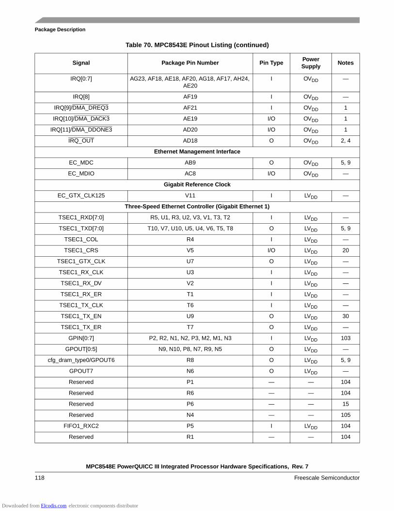
MPC8548E PowerQUICC III Integrated Processor Hardware Specifications, Rev. 7
118 Freescale Semiconductor
Package Description
IRQ[0:7] AG23, AF18, AE18, AF20, AG18, AF17, AH24, AE20
I OVDD —
IRQ[8] AF19 I OVDD —
IRQ[9]/DMA_DREQ3 AF21 I OVDD 1
IRQ[10]/DMA_DACK3 AE19 I/O OVDD 1
IRQ[11]/DMA_DDONE3 AD20 I/O OVDD 1
IRQ_OUT AD18 O OVDD 2, 4
Ethernet Management Interface
EC_MDC AB9 O OVDD 5, 9
EC_MDIO AC8 I/O OVDD —
Gigabit Reference Clock
EC_GTX_CLK125 V11 I LVDD —
Three-Speed Ethernet Controller (Gigabit Ethernet 1)
TSEC1_RXD[7:0] R5, U1, R3, U2, V3, V1, T3, T2 I LVDD —
TSEC1_TXD[7:0] T10, V7, U10, U5, U4, V6, T5, T8 O LVDD 5, 9
TSEC1_COL R4 I LVDD —
TSEC1_CRS V5 I/O LVDD 20
TSEC1_GTX_CLK U7 O LVDD —
TSEC1_RX_CLK U3 I LVDD —
TSEC1_RX_DV V2 I LVDD —
TSEC1_RX_ER T1 I LVDD —
TSEC1_TX_CLK T6 I LVDD —
TSEC1_TX_EN U9 O LVDD 30
TSEC1_TX_ER T7 O LVDD —
GPIN[0:7] P2, R2, N1, N2, P3, M2, M1, N3 I LVDD 103
GPOUT[0:5] N9, N10, P8, N7, R9, N5 O LVDD —
cfg_dram_type0/GPOUT6 R8 O LVDD 5, 9
GPOUT7 N6 O LVDD —
Reserved P1 — — 104
Reserved R6 — — 104
Reserved P6 — — 15
Reserved N4 — — 105
FIFO1_RXC2 P5 I LVDD 104
Reserved R1 — — 104
Table 70. MPC8543E Pinout Listing (continued)
Signal Package Pin Number Pin TypePowerSupply
Notes
Downloaded from Elcodis.com electronic components distributor
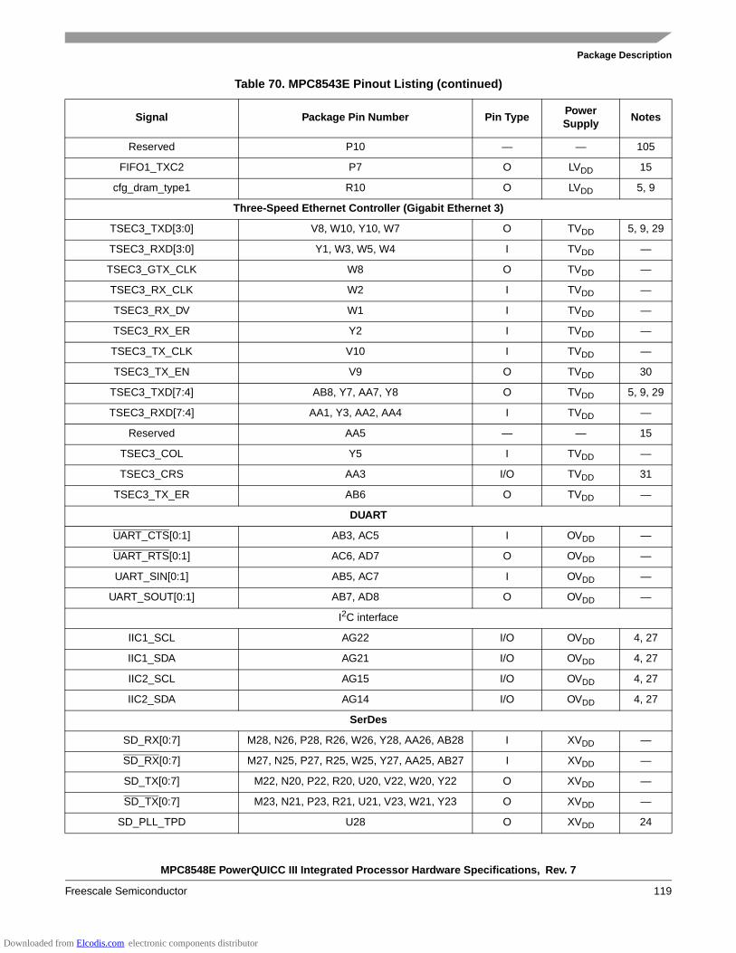
MPC8548E PowerQUICC III Integrated Processor Hardware Specifications, Rev. 7
Freescale Semiconductor 119
Package Description
Reserved P10 — — 105
FIFO1_TXC2 P7 O LVDD 15
cfg_dram_type1 R10 O LVDD 5, 9
Three-Speed Ethernet Controller (Gigabit Ethernet 3)
TSEC3_TXD[3:0] V8, W10, Y10, W7 O TVDD 5, 9, 29
TSEC3_RXD[3:0] Y1, W3, W5, W4 I TVDD —
TSEC3_GTX_CLK W8 O TVDD —
TSEC3_RX_CLK W2 I TVDD —
TSEC3_RX_DV W1 I TVDD —
TSEC3_RX_ER Y2 I TVDD —
TSEC3_TX_CLK V10 I TVDD —
TSEC3_TX_EN V9 O TVDD 30
TSEC3_TXD[7:4] AB8, Y7, AA7, Y8 O TVDD 5, 9, 29
TSEC3_RXD[7:4] AA1, Y3, AA2, AA4 I TVDD —
Reserved AA5 — — 15
TSEC3_COL Y5 I TVDD —
TSEC3_CRS AA3 I/O TVDD 31
TSEC3_TX_ER AB6 O TVDD —
DUART
UART_CTS[0:1] AB3, AC5 I OVDD —
UART_RTS[0:1] AC6, AD7 O OVDD —
UART_SIN[0:1] AB5, AC7 I OVDD —
UART_SOUT[0:1] AB7, AD8 O OVDD —
I2C interface
IIC1_SCL AG22 I/O OVDD 4, 27
IIC1_SDA AG21 I/O OVDD 4, 27
IIC2_SCL AG15 I/O OVDD 4, 27
IIC2_SDA AG14 I/O OVDD 4, 27
SerDes
SD_RX[0:7] M28, N26, P28, R26, W26, Y28, AA26, AB28 I XVDD —
SD_RX[0:7] M27, N25, P27, R25, W25, Y27, AA25, AB27 I XVDD —
SD_TX[0:7] M22, N20, P22, R20, U20, V22, W20, Y22 O XVDD —
SD_TX[0:7] M23, N21, P23, R21, U21, V23, W21, Y23 O XVDD —
SD_PLL_TPD U28 O XVDD 24
Table 70. MPC8543E Pinout Listing (continued)
Signal Package Pin Number Pin TypePowerSupply
Notes
Downloaded from Elcodis.com electronic components distributor

MPC8548E PowerQUICC III Integrated Processor Hardware Specifications, Rev. 7
120 Freescale Semiconductor
Package Description
SD_REF_CLK T28 I XVDD —
SD_REF_CLK T27 I XVDD —
Reserved AC1, AC3 — — 2
Reserved M26, V28 — — 32
Reserved M25, V27 — — 34
Reserved M20, M21, T22, T23 — — 38
General-Purpose Output
GPOUT[24:31] K26, K25, H27, G28, H25, J26, K24, K23 O BVDD —
System Control
HRESET AG17 I OVDD —
HRESET_REQ AG16 O OVDD 29
SRESET AG20 I OVDD —
CKSTP_IN AA9 I OVDD —
CKSTP_OUT AA8 O OVDD 2, 4
Debug
TRIG_IN AB2 I OVDD —
TRIG_OUT/READY/QUIESCE AB1 O OVDD 6, 9, 19, 29
MSRCID[0:1] AE4, AG2 O OVDD 5, 6, 9
MSRCID[2:4] AF3, AF1, AF2 O OVDD 6, 19, 29
MDVAL AE5 O OVDD 6
CLK_OUT AE21 O OVDD 11
Clock
RTC AF16 I OVDD —
SYSCLK AH17 I OVDD —
JTAG
TCK AG28 I OVDD —
TDI AH28 I OVDD 12
TDO AF28 O OVDD 11
TMS AH27 I OVDD 12
TRST AH23 I OVDD 12
DFT
L1_TSTCLK AC25 I OVDD 25
L2_TSTCLK AE22 I OVDD 25
Table 70. MPC8543E Pinout Listing (continued)
Signal Package Pin Number Pin TypePowerSupply
Notes
Downloaded from Elcodis.com electronic components distributor
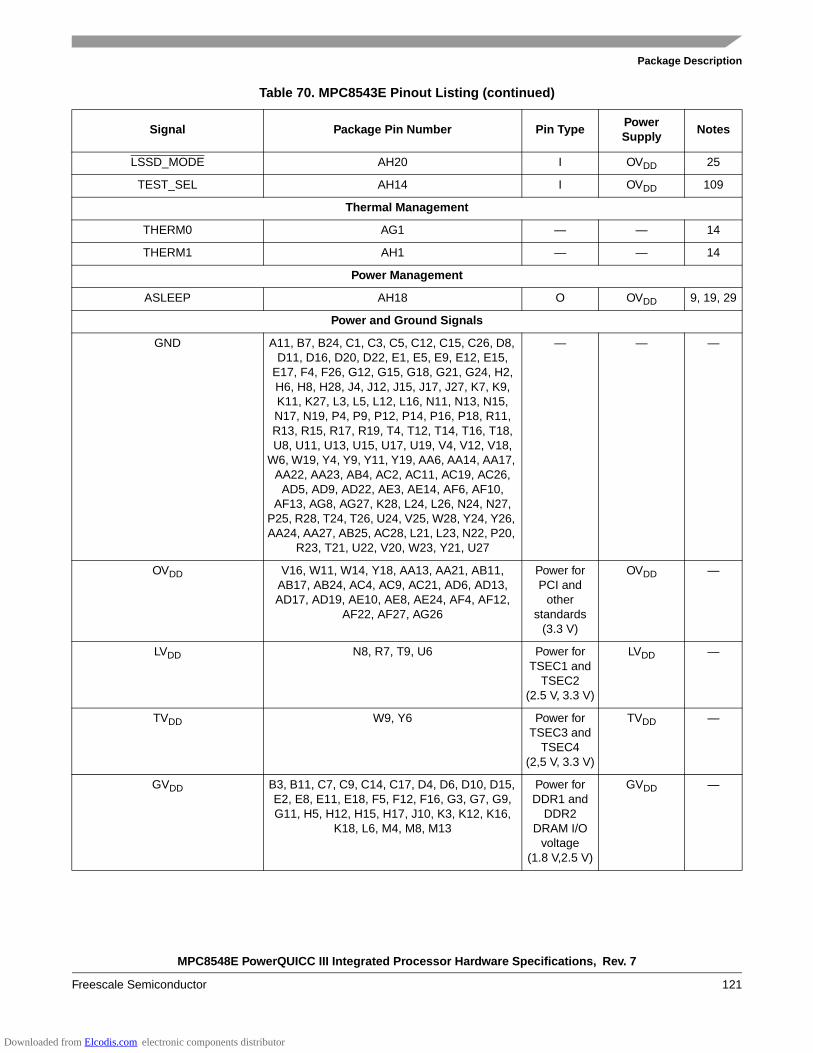
MPC8548E PowerQUICC III Integrated Processor Hardware Specifications, Rev. 7
Freescale Semiconductor 121
Package Description
LSSD_MODE AH20 I OVDD 25
TEST_SEL AH14 I OVDD 109
Thermal Management
THERM0 AG1 — — 14
THERM1 AH1 — — 14
Power Management
ASLEEP AH18 O OVDD 9, 19, 29
Power and Ground Signals
GND A11, B7, B24, C1, C3, C5, C12, C15, C26, D8, D11, D16, D20, D22, E1, E5, E9, E12, E15,
E17, F4, F26, G12, G15, G18, G21, G24, H2, H6, H8, H28, J4, J12, J15, J17, J27, K7, K9, K11, K27, L3, L5, L12, L16, N11, N13, N15, N17, N19, P4, P9, P12, P14, P16, P18, R11, R13, R15, R17, R19, T4, T12, T14, T16, T18, U8, U11, U13, U15, U17, U19, V4, V12, V18,
W6, W19, Y4, Y9, Y11, Y19, AA6, AA14, AA17, AA22, AA23, AB4, AC2, AC11, AC19, AC26,
AD5, AD9, AD22, AE3, AE14, AF6, AF10, AF13, AG8, AG27, K28, L24, L26, N24, N27,
P25, R28, T24, T26, U24, V25, W28, Y24, Y26, AA24, AA27, AB25, AC28, L21, L23, N22, P20,
R23, T21, U22, V20, W23, Y21, U27
— — —
OVDD V16, W11, W14, Y18, AA13, AA21, AB11, AB17, AB24, AC4, AC9, AC21, AD6, AD13, AD17, AD19, AE10, AE8, AE24, AF4, AF12,
AF22, AF27, AG26
Power for PCI and
other standards
(3.3 V)
OVDD —
LVDD N8, R7, T9, U6 Power for TSEC1 and
TSEC2(2.5 V, 3.3 V)
LVDD —
TVDD W9, Y6 Power for TSEC3 and
TSEC4(2,5 V, 3.3 V)
TVDD —
GVDD B3, B11, C7, C9, C14, C17, D4, D6, D10, D15, E2, E8, E11, E18, F5, F12, F16, G3, G7, G9, G11, H5, H12, H15, H17, J10, K3, K12, K16,
K18, L6, M4, M8, M13
Power for DDR1 and
DDR2 DRAM I/O
voltage (1.8 V,2.5 V)
GVDD —
Table 70. MPC8543E Pinout Listing (continued)
Signal Package Pin Number Pin TypePowerSupply
Notes
Downloaded from Elcodis.com electronic components distributor

MPC8548E PowerQUICC III Integrated Processor Hardware Specifications, Rev. 7
122 Freescale Semiconductor
Package Description
BVDD C21, C24, C27, E20, E25, G19, G23, H26, J20 Power for local bus
(1.8 V, 2.5 V, 3.3 V)
BVDD —
VDD M19, N12, N14, N16, N18, P11, P13, P15, P17, P19, R12, R14, R16, R18, T11, T13, T15, T17,
T19, U12, U14, U16, U18, V17, V19
Power for core (1.1 V)
VDD —
SVDD L25, L27, M24, N28, P24, P26, R24, R27, T25, V24, V26, W24, W27, Y25, AA28, AC27
Core power for SerDes
transceivers(1.1 V)
SVDD —
XVDD L20, L22, N23, P21, R22, T20, U23, V21, W22, Y20
Pad power for SerDes
transceivers(1.1 V)
XVDD —
AVDD_LBIU J28 Power for local bus
PLL(1.1 V)
— 26
AVDD_PCI1 AH21 Power for PCI1 PLL
(1.1 V)
— 26
AVDD_PCI2 AH22 Power for PCI2 PLL
(1.1 V)
— 26
AVDD_CORE AH15 Power for e500 PLL
(1.1 V)
— 26
AVDD_PLAT AH19 Power for CCB PLL
(1.1 V)
— 26
AVDD_SRDS U25 Power for SRDSPLL
(1.1 V)
— 26
SENSEVDD M14 O VDD 13
SENSEVSS M16 — — 13
Analog Signals
MVREF A18 IReference
voltage signal for
DDR
MVREF —
SD_IMP_CAL_RX L28 I 200 Ω (±1%)to GND
—
Table 70. MPC8543E Pinout Listing (continued)
Signal Package Pin Number Pin TypePowerSupply
Notes
Downloaded from Elcodis.com electronic components distributor
MPC8548E PowerQUICC III Integrated Processor Hardware Specifications, Rev. 7
Freescale Semiconductor 123
Clocking
19 ClockingThis section describes the PLL configuration of the MPC8548E. Note that the platform clock is identical to the core complex bus (CCB) clock.
19.1 Clock RangesTable 71 through Table 73 provide the clocking specifications for the processor cores and Table 74, through Table 76 provide the clocking specifications for the memory bus.
SD_IMP_CAL_TX AB26 I 100 Ω (±1%)to GND
—
SD_PLL_TPA U26 O AVDD_SRDS 24
Note: All note references in this table use the same numbers as those for Table 67. Refer to Table 67 for the meanings of these notes.
Table 71. Processor Core Clocking Specifications (MPC8548E and MPC8547E)
Characteristic
Maximum Processor Core Frequency
Unit Notes1000 MHz 1200 MHz 1333 MHz
Min Max Min Max Min Max
e500 core processor frequency 800 1000 800 1200 800 1333 MHz 1, 2
Notes:1. Caution: The CCB to SYSCLK ratio and e500 core to CCB ratio settings must be chosen such that the resulting SYSCLK
frequency, e500 (core) frequency, and CCB frequency do not exceed their respective maximum or minimum operating frequencies. Refer to Section 19.2, “CCB/SYSCLK PLL Ratio,” and Section 19.3, “e500 Core PLL Ratio,” for ratio settings.
2.)The minimum e500 core frequency is based on the minimum platform frequency of 333 MHz.
Table 72. Processor Core Clocking Specifications (MPC8545E)
Characteristic
Maximum Processor Core Frequency
Unit Notes800 MHz 1000 MHz 1200 MHz
Min Max Min Max Min Max
e500 core processor frequency 800 800 800 1000 800 1200 MHz 1, 2
Notes:1. Caution: The CCB to SYSCLK ratio and e500 core to CCB ratio settings must be chosen such that the resulting SYSCLK
frequency, e500 (core) frequency, and CCB frequency do not exceed their respective maximum or minimum operating frequencies. Refer to Section 19.2, “CCB/SYSCLK PLL Ratio,” and Section 19.3, “e500 Core PLL Ratio,” for ratio settings.
2.)The minimum e500 core frequency is based on the minimum platform frequency of 333 MHz.
Table 70. MPC8543E Pinout Listing (continued)
Signal Package Pin Number Pin TypePowerSupply
Notes
Downloaded from Elcodis.com electronic components distributor

MPC8548E PowerQUICC III Integrated Processor Hardware Specifications, Rev. 7
124 Freescale Semiconductor
Clocking
Table 73. Processor Core Clocking Specifications (MPC8543E)
Characteristic
Maximum Processor Core Frequency
Unit Notes800 MHz 1000 MHz
Min Max Min Max
e500 core processor frequency 800 800 800 1000 MHz 1, 2
Notes:1. Caution: The CCB to SYSCLK ratio and e500 core to CCB ratio settings must be chosen such that the resulting SYSCLK
frequency, e500 (core) frequency, and CCB frequency do not exceed their respective maximum or minimum operating frequencies. Refer to Section 19.2, “CCB/SYSCLK PLL Ratio,” and Section 19.3, “e500 Core PLL Ratio,” for ratio settings.
2.)The minimum e500 core frequency is based on the minimum platform frequency of 333 MHz.
Table 74. Memory Bus Clocking Specifications (MPC8548E and MPC8547E)
Characteristic
Maximum Processor Core Frequency
Unit Notes1000, 1200, 1333 MHz
Min Max
Memory bus clock speed 166 266 MHz 1, 2
Notes:1. Caution: The CCB clock to SYSCLK ratio and e500 core to CCB clock ratio settings must be chosen such that the resulting
SYSCLK frequency, e500 (core) frequency, and CCB clock frequency do not exceed their respective maximum or minimum operating frequencies. Refer to Section 19.2, “CCB/SYSCLK PLL Ratio,” and Section 19.3, “e500 Core PLL Ratio,” for ratio settings.
2. The memory bus speed is half of the DDR/DDR2 data rate, hence, half of the platform clock frequency.
Table 75. Memory Bus Clocking Specifications (MPC8545E)
Characteristic
Maximum Processor Core Frequency
Unit Notes800, 1000, 1200 MHz
Min Max
Memory bus clock speed 166 200 MHz 1, 2
Notes:1. Caution: The CCB clock to SYSCLK ratio and e500 core to CCB clock ratio settings must be chosen such that the resulting
SYSCLK frequency, e500 (core) frequency, and CCB clock frequency do not exceed their respective maximum or minimum operating frequencies. Refer to Section 19.2, “CCB/SYSCLK PLL Ratio,” and Section 19.3, “e500 Core PLL Ratio,” for ratio settings.
2. The memory bus speed is half of the DDR/DDR2 data rate, hence, half of the platform clock frequency.
Downloaded from Elcodis.com electronic components distributor

MPC8548E PowerQUICC III Integrated Processor Hardware Specifications, Rev. 7
Freescale Semiconductor 125
Clocking
19.2 CCB/SYSCLK PLL Ratio The CCB clock is the clock that drives the e500 core complex bus (CCB), and is also called the platform clock. The frequency of the CCB is set using the following reset signals, as shown in Table 77:
• SYSCLK input signal• Binary value on LA[28:31] at power up
Note that there is no default for this PLL ratio; these signals must be pulled to the desired values. Also note that the DDR data rate is the determining factor in selecting the CCB bus frequency, since the CCB frequency must equal the DDR data rate.
For specifications on the PCI_CLK, refer to the PCI 2.2 Specification.
Table 76. Memory Bus Clocking Specifications (MPC8543E)
Characteristic
Maximum Processor Core Frequency
Unit Notes800, 1000 MHz
Min Max
Memory bus clock speed 166 200 MHz 1, 2
Notes:1. Caution: The CCB clock to SYSCLK ratio and e500 core to CCB clock ratio settings must be chosen such that the resulting
SYSCLK frequency, e500 (core) frequency, and CCB clock frequency do not exceed their respective maximum or minimum operating frequencies. Refer to Section 19.2, “CCB/SYSCLK PLL Ratio,” and Section 19.3, “e500 Core PLL Ratio,” for ratio settings.
2. The memory bus speed is half of the DDR/DDR2 data rate, hence, half of the platform clock frequency.
Table 77. CCB Clock Ratio
Binary Value of LA[28:31] Signals CCB:SYSCLK Ratio Binary Value of LA[28:31] Signals CCB:SYSCLK Ratio
0000 16:1 1000 8:1
0001 Reserved 1001 9:1
0010 2:1 1010 10:1
0011 3:1 1011 Reserved
0100 4:1 1100 12:1
0101 5:1 1101 20:1
0110 6:1 1110 Reserved
0111 Reserved 1111 Reserved
Downloaded from Elcodis.com electronic components distributor

MPC8548E PowerQUICC III Integrated Processor Hardware Specifications, Rev. 7
126 Freescale Semiconductor
Thermal
19.3 e500 Core PLL RatioTable 78 describes the clock ratio between the e500 core complex bus (CCB) and the e500 core clock. This ratio is determined by the binary value of LBCTL, LALE, and LGPL2 at power up, as shown in Table 78.
19.4 Frequency OptionsTable 79 shows the expected frequency values for the platform frequency when using a CCB clock to SYSCLK ratio in comparison to the memory bus clock speed.
20 ThermalThis section describes the thermal specifications of the MPC8548.
Table 78. e500 Core to CCB Clock Ratio
Binary Value ofLBCTL, LALE, LGPL2
Signalse500 core:CCB Clock Ratio
Binary Value ofLBCTL, LALE, LGPL2
Signalse500 core:CCB Clock Ratio
000 4:1 100 2:1
001 9:2 101 5:2
010 Reserved 110 3:1
011 3:2 111 7:2
Table 79. Frequency Options of SYSCLK with Respect to Memory Bus Speeds
CCB to SYSCLK Ratio
SYSCLK (MHz)
16.66 25 33.33 41.66 66.66 83 100 111 133.33
Platform/CCB Frequency (MHz)
2
3 333 400
4 333 400 445 533
5 333 415 500
6 400 500
8 333 533
9 375
10 333 417
12 400 500
16 400 533
20 333 500
Note: Due to errata Gen 13, the max sys clk frequency should not exceed 100 MHz if the core clk frequency is below 1200 MHz.
Downloaded from Elcodis.com electronic components distributor

MPC8548E PowerQUICC III Integrated Processor Hardware Specifications, Rev. 7
Freescale Semiconductor 127
Thermal
20.1 Thermal for Version 2.0 Silicon HiCTE FC-CBGA with Full LidThis section describes the thermal specifications for the HiCTE FC-CBGA package for revision 2.0 silicon.
Table 80 shows the package thermal characteristics.
20.2 Thermal for Version 2.1.1 and 2.1.2 Silicon FC-PBGA with Full LidThis section describes the thermal specifications for the FC-PBGA package for revision 2.1.1 silicon.
Table 81 shows the package thermal characteristics.
Table 80. Package Thermal Characteristics for HiCTE FC-CBGA
Characteristic JEDEC Board Symbol Value Unit Notes
Die junction-to-ambient (natural convection) Single-layer board (1s) RθJA 17 °C/W 1, 2
Die junction-to-ambient (natural convection) Four-layer board (2s2p) RθJA 12 °C/W 1, 2
Die junction-to-ambient (200 ft/min) Single-layer board (1s) RθJA 11 °C/W 1, 2
Die junction-to-ambient (200 ft/min) Four-layer board (2s2p) RθJA 8 °C/W 1, 2
Die junction-to-board N/A RθJB 3 °C/W 3
Die junction-to-case N/A RθJC 0.8 °C/W 4
Notes:1. Junction temperature is a function of die size, on-chip power dissipation, package thermal resistance, mounting site (board)
temperature, ambient temperature, airflow, power dissipation of other components on the board, and board thermal resistance.
2. Per JEDEC JESD51-6 with the board (JESD51-7) horizontal.3. Thermal resistance between the die and the printed-circuit board per JEDEC JESD51-8. Board temperature is measured on
the top surface of the board near the package.4. Thermal resistance between the die and the case top surface as measured by the cold plate method (MIL SPEC-883 Method
1012.1). The cold plate temperature is used for the case temperature, measured value includes the thermal resistance of the interface layer.
Table 81. Package Thermal Characteristics for FC-PBGA
Characteristic JEDEC Board Symbol Value Unit Notes
Die junction-to-ambient (natural convection) Single-layer board (1s) RθJA 18 °C/W 1, 2
Die junction-to-ambient (natural convection) Four-layer board (2s2p) RθJA 13 °C/W 1, 2
Die junction-to-ambient (200 ft/min) Single-layer board (1s) RθJA 13 °C/W 1, 2
Die junction-to-ambient (200 ft/min) Four-layer board (2s2p) RθJA 9 °C/W 1, 2
Die junction-to-board N/A RθJB 5 °C/W 3
Downloaded from Elcodis.com electronic components distributor

MPC8548E PowerQUICC III Integrated Processor Hardware Specifications, Rev. 7
128 Freescale Semiconductor
System Design Information
20.3 Heat Sink SolutionEvery system application has different conditions that the thermal management solution must solve. As such, providing a recommended heat sink has not been found to be very useful. When a heat sink is chosen, give special consideration to the mounting technique. Mounting the heat sink to the printed-circuit board is the recommended procedure using a maximum of 10 lbs force (45 Newtons) perpendicular to the package and board. Clipping the heat sink to the package is not recommended.
21 System Design InformationThis section provides electrical design recommendations for successful application of the MPC8548E.
21.1 System ClockingThis device includes five PLLs, as follows:
1. The platform PLL generates the platform clock from the externally supplied SYSCLK input. The frequency ratio between the platform and SYSCLK is selected using the platform PLL ratio configuration bits as described in Section 19.2, “CCB/SYSCLK PLL Ratio.”
2. The e500 core PLL generates the core clock as a slave to the platform clock. The frequency ratio between the e500 core clock and the platform clock is selected using the e500 PLL ratio configuration bits as described in Section 19.3, “e500 Core PLL Ratio.”
3. The PCI PLL generates the clocking for the PCI bus.4. The local bus PLL generates the clock for the local bus. 5. There is a PLL for the SerDes block.
21.2 PLL Power Supply FilteringEach of the PLLs listed above is provided with power through independent power supply pins (AVDD_PLAT, AVDD_CORE, AVDD_PCI, AVDD_LBIU, and AVDD_SRDS, respectively). The AVDD level should always be equivalent to VDD, and preferably these voltages are derived directly from VDD through a low frequency filter scheme such as the following.
Die junction-to-case N/A RθJC 0.8 °C/W 4
Notes:1. Junction temperature is a function of die size, on-chip power dissipation, package thermal resistance, mounting site (board)
temperature, ambient temperature, airflow, power dissipation of other components on the board, and board thermal resistance.
2. Per JEDEC JESD51-6 with the board (JESD51-7) horizontal.3. Thermal resistance between the die and the printed circuit board per JEDEC JESD51-8. Board temperature is measured on
the top surface of the board near the package.4. Thermal resistance between the die and the case top surface as measured by the cold plate method (MIL SPEC-883 Method
1012.1). The cold plate temperature is used for the case temperature, measured value includes the thermal resistance of the interface layer.
Table 81. Package Thermal Characteristics for FC-PBGA (continued)
Characteristic JEDEC Board Symbol Value Unit Notes
Downloaded from Elcodis.com electronic components distributor
MPC8548E PowerQUICC III Integrated Processor Hardware Specifications, Rev. 7
Freescale Semiconductor 129
System Design Information
There are a number of ways to reliably provide power to the PLLs, but the recommended solution is to provide independent filter circuits per PLL power supply as illustrated in Figure 56, one to each of the AVDD pins. By providing independent filters to each PLL the opportunity to cause noise injection from one PLL to the other is reduced.
This circuit is intended to filter noise in the PLLs resonant frequency range from a 500 kHz to 10 MHz range. It should be built with surface mount capacitors with minimum Effective Series Inductance (ESL). Consistent with the recommendations of Dr. Howard Johnson in High Speed Digital Design: A Handbook of Black Magic (Prentice Hall, 1993), multiple small capacitors of equal value are recommended over a single large value capacitor.
Each circuit should be placed as close as possible to the specific AVDD pin being supplied to minimize noise coupled from nearby circuits. It should be possible to route directly from the capacitors to the AVDD pin, which is on the periphery of the footprint, without the inductance of vias.
Figure 56 through Figure 58 shows the PLL power supply filter circuits.
Figure 56. PLL Power Supply Filter Circuit with PLAT Pins
Figure 57. PLL Power Supply Filter Circuit with CORE Pins
Figure 58. PLL Power Supply Filter Circuit with PCI/LBIU Pins
The AVDD_SRDS signal provides power for the analog portions of the SerDes PLL. To ensure stability of the internal clock, the power supplied to the PLL is filtered using a circuit similar to the one shown in following figure. For maximum effectiveness, the filter circuit is placed as closely as possible to the AVDD_SRDS ball to ensure it filters out as much noise as possible. The ground connection should be near the AVDD_SRDS ball. The 0.003-µF capacitor is closest to the ball, followed by the two 2.2 µF capacitors, and finally the 1 Ω resistor to the board supply plane. The capacitors are connected from AVDD_SRDS to the ground plane. Use ceramic chip capacitors with the highest possible self-resonant frequency. All traces should be kept short, wide and direct.
VDD AVDD_PLAT
2.2 µF 2.2 µF
GNDLow ESL Surface Mount Capacitors
150 Ω
VDD AVDD_CORE 2.2 µF 2.2 µF
GNDLow ESL Surface Mount Capacitors
180 Ω
VDD AVDD_PCI/AVDD_LBIU 2.2 µF 2.2 µF
GNDLow ESL Surface Mount Capacitors
10 Ω
Downloaded from Elcodis.com electronic components distributor

MPC8548E PowerQUICC III Integrated Processor Hardware Specifications, Rev. 7
130 Freescale Semiconductor
System Design Information
Figure 59. SerDes PLL Power Supply Filter
Note the following:• AVDD_SRDS should be a filtered version of SVDD.• Signals on the SerDes interface are fed from the XVDD power plane.
21.3 Decoupling RecommendationsDue to large address and data buses, and high operating frequencies, the device can generate transient power surges and high frequency noise in its power supply, especially while driving large capacitive loads. This noise must be prevented from reaching other components in the MPC8548E system, and the device itself requires a clean, tightly regulated source of power. Therefore, it is recommended that the system designer place at least one decoupling capacitor at each VDD, TVDD, BVDD, OVDD, GVDD, and LVDD pin of the device. These decoupling capacitors should receive their power from separate VDD, TVDD, BVDD, OVDD, GVDD, LVDD, and GND power planes in the PCB, utilizing short low impedance traces to minimize inductance. Capacitors must be placed directly under the device using a standard escape pattern as much as possible. If some caps are to be placed surrounding the part it should be routed with large trace to minimize the inductance.
These capacitors should have a value of 0.1 µF. Only ceramic SMT (surface mount technology) capacitors should be used to minimize lead inductance, preferably 0402 or 0603 sizes.
In addition, it is recommended that there be several bulk storage capacitors distributed around the PCB, feeding the VDD, TVDD, BVDD, OVDD, GVDD, and LVDD, planes, to enable quick recharging of the smaller chip capacitors. These bulk capacitors should have a low ESR (equivalent series resistance) rating to ensure the quick response time necessary. They should also be connected to the power and ground planes through two vias to minimize inductance. Suggested bulk capacitors—100–330 µF (AVX TPS tantalum or Sanyo OSCON). However, customers should work directly with their power regulator vendor for best values, types and quantity of bulk capacitors.
21.4 SerDes Block Power Supply Decoupling RecommendationsThe SerDes block requires a clean, tightly regulated source of power (SVDD and XVDD) to ensure low jitter on transmit and reliable recovery of data in the receiver. An appropriate decoupling scheme is outlined below.
Only surface mount technology (SMT) capacitors should be used to minimize inductance. Connections from all capacitors to power and ground should be done with multiple vias to further reduce inductance.
• First, the board should have at least 10 × 10-nF SMT ceramic chip capacitors as close as possible to the supply balls of the device. Where the board has blind vias, these capacitors should be placed
2.2 µF 1 0.003 µF
1.0 ΩAVDD_SRDS
Note: 1. An 0805 sized capacitor is recommended for system initial bring-up.
SVDD
2.2 µF 1
GND
Downloaded from Elcodis.com electronic components distributor
MPC8548E PowerQUICC III Integrated Processor Hardware Specifications, Rev. 7
Freescale Semiconductor 131
System Design Information
directly below the chip supply and ground connections. Where the board does not have blind vias, these capacitors should be placed in a ring around the device as close to the supply and ground connections as possible.
• Second, there should be a 1-µF ceramic chip capacitor from each SerDes supply (SVDD and XVDD) to the board ground plane on each side of the device. This should be done for all SerDes supplies.
• Third, between the device and any SerDes voltage regulator there should be a 10-µF, low equivalent series resistance (ESR) SMT tantalum chip capacitor and a 100-µF, low ESR SMT tantalum chip capacitor. This should be done for all SerDes supplies.
21.5 Connection RecommendationsTo ensure reliable operation, it is highly recommended to connect unused inputs to an appropriate signal level. All unused active low inputs should be tied to VDD, TVDD, BVDD, OVDD, GVDD, and LVDD, as required. All unused active high inputs should be connected to GND. All NC (no-connect) signals must remain unconnected. Power and ground connections must be made to all external VDD, TVDD, BVDD, OVDD, GVDD, LVDD, and GND pins of the device.
21.6 Pull-Up and Pull-Down Resistor RequirementsThe MPC8548E requires weak pull-up resistors (2–10 kΩ is recommended) on open drain type pins including I2C pins and PIC (interrupt) pins.
Correct operation of the JTAG interface requires configuration of a group of system control pins as demonstrated in Figure 62. Care must be taken to ensure that these pins are maintained at a valid deasserted state under normal operating conditions as most have asynchronous behavior and spurious assertion gives unpredictable results.
The following pins must not be pulled down during power-on reset: TSEC3_TXD[3], HRESET_REQ, TRIG_OUT/READY/QUIESCE, MSRCID[2:4], ASLEEP. The DMA_DACK[0:1], and TEST_SEL/ TEST_SEL pins must be set to a proper state during POR configuration. Refer to the pinlist table of the individual device for more detailsRefer to the PCI 2.2 specification for all pull ups required for PCI.
21.7 Output Buffer DC ImpedanceThe MPC8548E drivers are characterized over process, voltage, and temperature. For all buses, the driver is a push-pull single-ended driver type (open drain for I2C).
To measure Z0 for the single-ended drivers, an external resistor is connected from the chip pad to OVDD or GND. Then, the value of each resistor is varied until the pad voltage is OVDD/2 (see Figure 60). The output impedance is the average of two components, the resistances of the pull-up and pull-down devices. When data is held high, SW1 is closed (SW2 is open) and RP is trimmed until the voltage at the pad equals OVDD/2. RP then becomes the resistance of the pull-up devices. RP and RN are designed to be close to each other in value. Then, Z0 = (RP + RN)/2.
Downloaded from Elcodis.com electronic components distributor

MPC8548E PowerQUICC III Integrated Processor Hardware Specifications, Rev. 7
132 Freescale Semiconductor
System Design Information
Figure 60. Driver Impedance Measurement
Table 82 summarizes the signal impedance targets. The driver impedances are targeted at minimum VDD, nominal OVDD, 105°C.
21.8 Configuration Pin MuxingThe MPC8548E provides the user with power-on configuration options which can be set through the use of external pull-up or pull-down resistors of 4.7 kΩ on certain output pins (see customer visible configuration pins). These pins are generally used as output only pins in normal operation.
While HRESET is asserted however, these pins are treated as inputs. The value presented on these pins while HRESET is asserted, is latched when HRESET deasserts, at which time the input receiver is disabled and the I/O circuit takes on its normal function. Most of these sampled configuration pins are equipped with an on-chip gated resistor of approximately 20 kΩ. This value should permit the 4.7-kΩ resistor to pull the configuration pin to a valid logic low level. The pull-up resistor is enabled only during HRESET (and for platform/system clocks after HRESET deassertion to ensure capture of the reset value). When the input receiver is disabled the pull-up is also, thus allowing functional operation of the pin as an output with minimal signal quality or delay disruption. The default value for all configuration bits treated this way has been encoded such that a high voltage level puts the device into the default state and external resistors are needed only when non-default settings are required by the user.
Careful board layout with stubless connections to these pull-down resistors coupled with the large value of the pull-down resistor should minimize the disruption of signal quality or speed for output pins thus configured.
Table 82. Impedance Characteristics
ImpedanceLocal Bus, Ethernet, DUART, Control,
Configuration, Power ManagementPCI DDR DRAM Symbol Unit
RN 43 Target 25 Target 20 Target Z0 W
RP 43 Target 25 Target 20 Target Z0 W
Note: Nominal supply voltages. See Table 1, Tj = 105°C.
OVDD
OGND
PadData
SW1
SW2
RN
RP
Downloaded from Elcodis.com electronic components distributor

MPC8548E PowerQUICC III Integrated Processor Hardware Specifications, Rev. 7
Freescale Semiconductor 133
System Design Information
The platform PLL ratio and e500 PLL ratio configuration pins are not equipped with these default pull-up devices.
21.9 JTAG Configuration SignalsCorrect operation of the JTAG interface requires configuration of a group of system control pins as demonstrated in Figure 62. Care must be taken to ensure that these pins are maintained at a valid deasserted state under normal operating conditions as most have asynchronous behavior and spurious assertion gives unpredictable results.
Boundary-scan testing is enabled through the JTAG interface signals. The TRST signal is optional in the IEEE 1149.1 specification, but it is provided on all processors built on Power Architecture technology. The device requires TRST to be asserted during power-on reset flow to ensure that the JTAG boundary logic does not interfere with normal chip operation. While the TAP controller can be forced to the reset state using only the TCK and TMS signals, generally systems assert TRST during the power-on reset flow. Simply tying TRST to HRESET is not practical because the JTAG interface is also used for accessing the common on-chip processor (COP), which implements the debug interface to the chip.
The COP function of these processors allow a remote computer system (typically, a PC with dedicated hardware and debugging software) to access and control the internal operations of the processor. The COP interface connects primarily through the JTAG port of the processor, with some additional status monitoring signals. The COP port requires the ability to independently assert HRESET or TRST in order to fully control the processor. If the target system has independent reset sources, such as voltage monitors, watchdog timers, power supply failures, or push-button switches, then the COP reset signals must be merged into these signals with logic.
The arrangement shown in Figure 62 allows the COP port to independently assert HRESET or TRST, while ensuring that the target can drive HRESET as well.
The COP interface has a standard header, shown in Figure 61, for connection to the target system, and is based on the 0.025" square-post, 0.100" centered header assembly (often called a Berg header). The connector typically has pin 14 removed as a connector key.
The COP header adds many benefits such as breakpoints, watchpoints, register and memory examination/modification, and other standard debugger features. An inexpensive option can be to leave the COP header unpopulated until needed.
There is no standardized way to number the COP header; so emulator vendors have issued many different pin numbering schemes. Some COP headers are numbered top-to-bottom then left-to-right, while others use left-to-right then top-to-bottom. Still others number the pins counter-clockwise from pin 1 (as with an IC). Regardless of the numbering scheme, the signal placement recommended in Figure 61 is common to all known emulators.
21.9.1 Termination of Unused SignalsFreescale recommends the following connections, when the JTAG interface and COP header are not used:
• TRST should be tied to HRESET through a 0 kΩ isolation resistor so that it is asserted when the system reset signal (HRESET) is asserted, ensuring that the JTAG scan chain is initialized during the power-on reset flow. Freescale recommends that the COP header be designed into the system
Downloaded from Elcodis.com electronic components distributor

MPC8548E PowerQUICC III Integrated Processor Hardware Specifications, Rev. 7
134 Freescale Semiconductor
System Design Information
as shown in Figure 62. If this is not possible, the isolation resistor allows future access to TRST in case a JTAG interface may need to be wired onto the system in future debug situations.
• No pull-up/pull-down is required for TDI, TMS, TDO, or TCK.
Figure 61. COP Connector Physical Pinout
3
13
9
5
1
6
10
15
11
7
16
12
8
4
KEYNo pin
1 2COP_TDO
COP_TDI
COP_RUN/STOP
NC
COP_TRST
COP_VDD_SENSE
COP_CHKSTP_IN
NC
NC
GND
COP_TCK
COP_TMS
COP_SRESET
COP_HRESET
COP_CHKSTP_OUT
Downloaded from Elcodis.com electronic components distributor
MPC8548E PowerQUICC III Integrated Processor Hardware Specifications, Rev. 7
Freescale Semiconductor 135
System Design Information
Figure 62. JTAG Interface Connection
HRESET
From TargetBoard Sources
COP_HRESET13
COP_SRESET
SRESET
NC
11
COP_VDD_SENSE26
5
15
10 Ω
10 kΩ
10 kΩ
COP_CHKSTP_INCKSTP_IN8
COP_TMS
COP_TDO
COP_TDI
COP_TCK
TMS
TDO
TDI
9
1
3
4COP_TRST
7
16
2
10
12
(if any)
CO
P H
ead
er
14 3
Notes:
3. The KEY location (pin 14) is not physically present on the COP header.
10 kΩ
TRST110 kΩ
10 kΩ
10 kΩ
CKSTP_OUTCOP_CHKSTP_OUT
3
13
9
5
1
6
10
15
11
7
16
12
8
4
KEYNo pin
COP ConnectorPhysical Pinout
1 2
NC
SRESET
2. Populate this with a 10−Ω resistor for short-circuit/current-limiting protection.
NC
OVDD
10 kΩ HRESET1
in order to fully control the processor as shown here.
4. Although pin 12 is defined as a No-Connect, some debug tools may use pin 12 as an additional GND pin for
1. The COP port and target board should be able to independently assert HRESET and TRST to the processor
improved signal integrity.
TCK
4
5
5. This switch is included as a precaution for BSDL testing. The switch should be closed to position A during BSDL testing to avoid accidentally asserting the TRST line. If BSDL testing is not being performed, this switch should be
10 kΩ
6
6. Asserting SRESET causes a machine check interrupt to the e500 core.
AB
closed to position B.
Downloaded from Elcodis.com electronic components distributor

MPC8548E PowerQUICC III Integrated Processor Hardware Specifications, Rev. 7
136 Freescale Semiconductor
System Design Information
21.10 Guidelines for High-Speed Interface TerminationThis section provides the guidelines for high-speed interface termination when the SerDes interface is entirely unused and when it is partly unused.
21.10.1 SerDes Interface Entirely UnusedIf the high-speed SerDes interface is not used at all, the unused pin should be terminated as described in this section.
The following pins must be left unconnected (float): • SD_TX[7:0] • SD_TX[7:0] • Reserved pins T22, T23, M20, M21
The following pins must be connected to GND:• SD_RX[7:0]• SD_RX[7:0]• SD_REF_CLK• SD_REF_CLK
NOTE
It is recommended to power down the unused lane through SRDSCR1[0:7] register (offset = 0xE_0F08) (This prevents the oscillations and holds the receiver output in a fixed state.) that maps to SERDES lane 0 to lane 7 accordingly.
Pins V28 and M26 must be tied to XVDD. Pins V27 and M25 must be tied to GND through a 300-Ω resistor.
In Rev 2.0 silicon, POR configuration pin cfg_srds_en on TSEC4_TXD[2]/TSEC3_TXD[6] can be used to power down SerDes block.
21.10.2 SerDes Interface Partly UnusedIf only part of the high-speed SerDes interface pins are used, the remaining high-speed serial I/O pins should be terminated as described in this section.
The following pins must be left unconnected (float) if not used: • SD_TX[7:0] • SD_TX[7:0]• Reserved pins: T22, T23, M20, M21
The following pins must be connected to GND if not used:• SD_RX[7:0]• SD_RX[7:0]• SD_REF_CLK• SD_REF_CLK
Downloaded from Elcodis.com electronic components distributor
MPC8548E PowerQUICC III Integrated Processor Hardware Specifications, Rev. 7
Freescale Semiconductor 137
Ordering Information
NOTEIt is recommended to power down the unused lane through SRDSCR1[0:7] register (offset = 0xE_0F08) (this prevents the oscillations and holds the receiver output in a fixed state) that maps to SERDES lane 0 to lane 7 accordingly.
Pins V28 and M26 must be tied to XVDD. Pins V27 and M25 must be tied to GND through a 300-Ω resistor.
21.11 Guideline for PCI Interface Termination PCI termination if PCI 1 or PCI 2 is not used at all.
Option 1
If PCI arbiter is enabled during POR:• All AD pins are driven to the stable states after POR. Therefore, all ADs pins can be floating.• All PCI control pins can be grouped together and tied to OVDD through a single 10-kΩ resistor.• It is optional to disable PCI block through DEVDISR register after POR reset.
Option 2
If PCI arbiter is disabled during POR:• All AD pins are in the input state. Therefore, all ADs pins need to be grouped together and tied to
OVDD through a single (or multiple) 10-kΩ resistor(s).• All PCI control pins can be grouped together and tied to OVDD through a single 10-kΩ resistor.• It is optional to disable PCI block through DEVDISR register after POR reset.
21.12 Guideline for LBIU TerminationIf the LBIU parity pins are not used, the following is the termination recommendation:
• For LDP[0:3]—tie them to ground or the power supply rail via a 4.7-kΩ resistor.• For LPBSE—tie it to the power supply rail via a 4.7-kΩ resistor (pull-up resistor).
22 Ordering InformationOrdering information for the parts fully covered by this specification document is provided in Section 22.1, “Part Numbers Fully Addressed by this Document.”
22.1 Part Numbers Fully Addressed by this DocumentTable 83 provides the Freescale part numbering nomenclature for the MPC8548E. Note that the individual part numbers correspond to a maximum processor core frequency. For available frequencies, contact your local Freescale sales office. In addition to the processor frequency, the part numbering scheme also
Downloaded from Elcodis.com electronic components distributor
MPC8548E PowerQUICC III Integrated Processor Hardware Specifications, Rev. 7
138 Freescale Semiconductor
Ordering Information
includes an application modifier which may specify special application conditions. Each part number also contains a revision code which refers to the die mask revision number.
Table 83. Part Numbering Nomenclature
MPC nnnnn t pp ff c r
ProductCode
Part Identifier
Temperature Package1, 2, 3 Processor Frequency4
Core Frequency
Silicon Version
MPC 8548E Blank = 0 to 105°CC = –40° to 105°C
HX = CBGAVU = Pb-free CBGA
PX = PBGAVT = Pb-free PBGA
AV = 15003
AU = 1333AT = 1200AQ = 1000
J = 533H = 5005
G = 400
Blank = Ver. 2.0(SVR = 0x80390020)
A = Ver. 2.1.1B = Ver. 2.1.2
(SVR = 0x80390021)
8548 Blank = Ver. 2.0(SVR = 0x80310020)
A = Ver. 2.1.1B = Ver. 2.1.2
(SVR = 0x80310021)
8547E AU = 1333AT = 1200AQ = 1000
J = 533G = 400
Blank = Ver. 2.0(SVR = 0x80390120)
A = Ver. 2.1.1B = Ver. 2.1.2
(SVR = 0x80390121)
8547 Blank = Ver. 2.0(SVR = 0x80390120)
A = Ver. 2.1.1B = Ver. 2.1.2
(SVR = 0x80310121)
8545E AT = 1200AQ = 1000AN = 800
G = 400 Blank = Ver. 2.0(SVR = 0x80390220)
A = Ver. 2.1.1B = Ver. 2.1.2
(SVR = 0x80390221)
8545 Blank = Ver. 2.0(SVR = 0x80310220)
A = Ver. 2.1.1B = Ver. 2.1.2
(SVR = 0x80310221)
8543E AQ = 1000AN = 800
Blank = Ver. 2.0(SVR = 0x803A0020)
A = Ver. 2.1.1B = Ver. 2.1.2
(SVR = 0x803A0021)
8543 Blank = Ver. 2.0(SVR = 0x80320020)
A = Ver. 2.1.1B = Ver. 2.1.2
(SVR = 0x80320021)
Downloaded from Elcodis.com electronic components distributor
MPC8548E PowerQUICC III Integrated Processor Hardware Specifications, Rev. 7
Freescale Semiconductor 139
Ordering Information
22.2 Part MarkingParts are marked as the example shown in Figure 63.
Figure 63. Part Marking for CBGA and PBGA Device
Notes: 1. See Section 18, “Package Description,” for more information on available package types.2. The HiCTE FC-CBGA package is available on only Version 2.0 of the device.3. The FC-PBGA package is available on only Version 2.1.1 and 2.1.2 of the device.4. Processor core frequencies supported by parts addressed by this specification only. Not all parts described in this
specification support all core frequencies. Additionally, parts addressed by part number specifications may support other maximum core frequencies.
5. This speed available only for silicon Version 2.1.1 and 2.1.2.
Table 83. Part Numbering Nomenclature
MPC nnnnn t pp ff c r
ProductCode
Part Identifier
Temperature Package1, 2, 3 Processor Frequency4
Core Frequency
Silicon Version
MMMMM CCCCC
Notes:
CCCCC is the country of assembly. This space is left blank if parts are assembled in the United States.
TWLYYWW is final test traceability code. MMMMM is 5 digit mask number.
MPC8548xxxxxxTWLYWW
YWWLAZ
YWWLAZ is assembly traceability code.
(F)
Downloaded from Elcodis.com electronic components distributor
MPC8548E PowerQUICC III Integrated Processor Hardware Specifications, Rev. 7
140 Freescale Semiconductor
Document Revision History
23 Document Revision HistoryTable 84 provides a revision history for the MPC8548E hardware specification.
Table 84. Document Revision History
Revision Date Substantive Change(s)
7 09/2010 • In Table 37, “MII Management AC Timing Specifications,” modified the min and max columns in the fifth row from “(16 × tptb_clk × 8) – 3” and “(16 × tptb_clk × 8) + 3” to “(16 × tCCB × 8) – 3” and “(16 × tCCB × 8) + 3.”
• In Table 67–Table 70, added note 114 to table and LGPL4/LGTA/LUPWAIT/LPBSE row. • Updated Figure 55, “Mechanical Dimensions and Bottom Surface Nomenclature of the HiCTE
FC-CBGA and FC-PBGA with Full Lid,” and figure notes.
6 12/2009 • In Section 5.1, “Power-On Ramp Rate” added explanation that Power-On Ramp Rate is required to avoid falsely triggering ESD circuitry.
• In Table 10 changed required ramp rate from 545 V/s for MVREF and VDD/XVDD/SVDD to 3500 V/s for MVREF and 4000 V/s for VDD.
• In Table 10 deleted ramp rate requirement for XVDD/SVDD. • In Table 10 footnote 1 changed voltage range of concern from 0–400 mV to 20–500mV. • In Table 10 added footnote 2 explaining that VDD voltage ramp rate is intended to control ramp rate of
AVDD pins.
5 10/2009 • In Table 27, ”GMII Receive AC Timing Specifications,” changed duty cycle specification from 40/60 to 35/75 for RX_CLK duty cycle.
• Updated tMDKHDX in Table 37, “MII Management AC Timing Specifications.” • Added a reference to Revision 2.1.2. • Updated Table 55, “MII Management AC Timing Specifications.” • Added Section 5.1, “Power-On Ramp Rate.”
4 04/2009 • In Table 1, “Absolute Maximum Ratings 1,” and in Table 2, “Recommended Operating Conditions,” moved text, “MII management voltage” from LVDD/TVDD to OVDD, added “Ethernet management” to OVDD row of input voltage section.
• In Table 5, “SYSCLK AC Timing Specifications,” added notes 7 and 8 to SYSCLK frequency and cycle time.
• In Table 36, “MII Management DC Electrical Characteristics,” changed all instances of LVDD/OVDD to OVDD.
• Modified Section 15, “High-Speed Serial Interfaces (HSSI),” to reflect that there is only one SerDes. • Modified DDR clk rate min from 133 to 166 MHz. • Modified note in Table 71, “Processor Core Clocking Specifications (MPC8548E and MPC8547E), “.” • In Table 52, “Differential Transmitter (TX) Output Specifications,” modified equations in Comments
column, and changed all instances of “LO” to “L0.” In addition, added note 8. • In Table 53, “Differential Receiver (RX) Input Specifications,” modified equations in Comments column,
and in note 3, changed “TRX-EYE-MEDIAN-to-MAX-JITTER,” to “TRX-EYE-MEDIAN-to-MAX-JITTER.” • Modified Table 79, “Frequency Options of SYSCLK with Respect to Memory Bus Speeds.” • Added a note on Section 4.1, “System Clock Timing,” to limit the SYSCLK to 100 MHz if the core
frequency is less than 1200 MHz • In Table 67, “MPC8548E Pinout ListingTable 68, “MPC8547E Pinout ListingTable 69, “MPC8545E
Pinout ListingTable 70, “MPC8543E Pinout Listing,” added note 5 to LA[28:31]. • Added note to Table 79, “Frequency Options of SYSCLK with Respect to Memory Bus Speeds.”
Downloaded from Elcodis.com electronic components distributor

MPC8548E PowerQUICC III Integrated Processor Hardware Specifications, Rev. 7
Freescale Semiconductor 141
Document Revision History
3 01/2009 • [Section 4.6, “Platform Frequency Requirements for PCI-Express and Serial RapidIO.” Changed minimum frequency equation to be 527 MHz for PCI x8.
• In Table 5, added note 7. • Section 4.5, “Platform to FIFO Restrictions.” Changed platform clock frequency to 4.2. • Section 8.1, “Enhanced Three-Speed Ethernet Controller (eTSEC)
(10/100/1Gb Mbps)—GMII/MII/TBI/RGMII/RTBI/RMII Electrical Characteristics.” Added MII after GMII and add ‘or 2.5 V’ after 3.3 V.
• In Table 23, modified table title to include GMII, MII, RMII, and TBI. • In Table 24 and Table 25, changed clock period minimum to 5.3. • In Table 25, added a note. • In Table 26, Table 27, Table 28, Table 29, and Table 30, removed subtitle from table title. • In Table 30 and Figure 15, changed all instances of PMA to TSECn. • In Section 8.2.5, “TBI Single-Clock Mode AC Specifications.” Replaced first paragraph. • In Table 34, Table 35, Figure 18, and Figure 20, changed all instances of REF_CLK to
TSECn_TX_CLK. • In Table 36, changed all instances of OVDD to LVDD/TVDD. • In Table 37, “MII Management AC Timing Specifications,” changed MDC minimum clock pulse width
high from 32 to 48 ns. • Added new section, Section 15, “High-Speed Serial Interfaces (HSSI).” • Section 16.1, “DC Requirements for PCI Express SD_REF_CLK and SD_REF_CLK.” Added new
paragraph. • Section 17.1, “DC Requirements for Serial RapidIO SD_REF_CLK and SD_REF_CLK.” Added new
paragraph. • Added information to Figure 63, both in figure and in note. • Section 21.3, “Decoupling Recommendations.” Modified the recommendation. • Table 83, “Part Numbering Nomenclature.” In Silicon Version column added Ver. 2.1.2.
2 04/2008 • Removed 1:1 support on Table 78, “e500 Core to CCB Clock Ratio.” • Removed MDM from Table 18, “DDR SDRAM Input AC Timing Specifications.” MDM is an Output. • Figure 56, “PLL Power Supply Filter Circuit with PLAT Pins” (AVDD_PLAT). • Figure 57, “PLL Power Supply Filter Circuit with CORE Pins” (AVDD_CORE). • Split Figure 58, “PLL Power Supply Filter Circuit with PCI/LBIU Pins,” (formerly called just “PLL Power
Supply Filter Circuit”) into three figures: the original (now specific for AVDD_PCI/AVDD_LBIU) and two new ones.
Table 84. Document Revision History (continued)
Revision Date Substantive Change(s)
Downloaded from Elcodis.com electronic components distributor
MPC8548E PowerQUICC III Integrated Processor Hardware Specifications, Rev. 7
142 Freescale Semiconductor
Document Revision History
1 10/2007 • Adjusted maximum SYSCLK frequency down in Table 5, “SYSCLK AC Timing Specifications” per device erratum GEN-13.
• Clarified notes to Table 6, “EC_GTX_CLK125 AC Timing Specifications.” • Added Section 4.4, “PCI/PCI-X Reference Clock Timing.” • Clarified descriptions and added PCI/PCI-X to Table 9, “PLL Lock Times.” • Removed support for 266 and 200 Mbps data rates per device erratum GEN-13 in Section 6, “DDR and
DDR2 SDRAM.” • Clarified Note 4 of Table 19, “DDR SDRAM Output AC Timing Specifications.” • Clarified the reference clock used in Section 7.2, “DUART AC Electrical Specifications.” • Corrected VIH(min) in Table 22, “GMII, MII, RMII, and TBI DC Electrical Characteristics.” • Corrected VIL(max) in Table 23, “GMII, MII, RMII, TBI, RGMII, RTBI, and FIFO DC Electrical
Characteristics.” • Removed DC parameters from Table 24, Table 25, Table 26, Table 27, Table 28, Table 29, Table 32,
Table 34, and Table 35. • Corrected VIH(min) in Table 36, “MII Management DC Electrical Characteristics.” • Corrected tMDC(min) in Table 37, “MII Management AC Timing Specifications.” • Updated parameter descriptions for tLBIVKH1, tLBIVKH2, tLBIXKH1, and tLBIXKH2 in Table 40, “Local Bus
Timing Parameters (BVDD = 3.3 V)—PLL Enabled” and Table 40, “Local Bus Timing Parameters (BVDD = 2.5 V)—PLL Enabled.”
• Updated parameter descriptions for tLBIVKH1, tLBIVKL2, tLBIXKH1, and tLBIXKL2 in Table 42, “Local Bus Timing Parameters—PLL Bypassed.” Note that tLBIVKL2 and tLBIXKL2 were previously labeled tLBIVKH2 and tLBIXKH2.
• Added LUPWAIT signal to Figure 23, “Local Bus Signals (PLL Enabled)” and Figure 24, “Local Bus Signals (PLL Bypass Mode).”
• Added LGTA signal to Figure 25, Figure 26, Figure 27 and Figure 28. • Corrected LUPWAIT assertion in Figure 26 and Figure 28. • Clarified the PCI reference clock in Section 14.2, “PCI/PCI-X AC Electrical Specifications” • Added Section 17.1, “Package Parameters.” • Added PBGA thermal information in Section 20.2, “Thermal for Version 2.1.1 and 2.1.2 Silicon
FC-PBGA with Full Lid.” • Updated.” • Updated Table 83, “Part Numbering Nomenclature.”
0 07/2007 • Initial Release
Table 84. Document Revision History (continued)
Revision Date Substantive Change(s)
Downloaded from Elcodis.com electronic components distributor

Document Number: MPC8548EECRev. 709/2010
Information in this document is provided solely to enable system and software
implementers to use Freescale Semiconductor products. There are no express or
implied copyright licenses granted hereunder to design or fabricate any integrated
circuits or integrated circuits based on the information in this document.
Freescale Semiconductor reserves the right to make changes without further notice to
any products herein. Freescale Semiconductor makes no warranty, representation or
guarantee regarding the suitability of its products for any particular purpose, nor does
Freescale Semiconductor assume any liability arising out of the application or use of
any product or circuit, and specifically disclaims any and all liability, including without
limitation consequential or incidental damages. “Typical” parameters which may be
provided in Freescale Semiconductor data sheets and/or specifications can and do
vary in different applications and actual performance may vary over time. All operating
parameters, including “Typicals” must be validated for each customer application by
customer’s technical experts. Freescale Semiconductor does not convey any license
under its patent rights nor the rights of others. Freescale Semiconductor products are
not designed, intended, or authorized for use as components in systems intended for
surgical implant into the body, or other applications intended to support or sustain life,
or for any other application in which the failure of the Freescale Semiconductor product
could create a situation where personal injury or death may occur. Should Buyer
purchase or use Freescale Semiconductor products for any such unintended or
unauthorized application, Buyer shall indemnify and hold Freescale Semiconductor
and its officers, employees, subsidiaries, affiliates, and distributors harmless against all
claims, costs, damages, and expenses, and reasonable attorney fees arising out of,
directly or indirectly, any claim of personal injury or death associated with such
unintended or unauthorized use, even if such claim alleges that Freescale
Semiconductor was negligent regarding the design or manufacture of the part.
How to Reach Us:
Home Page: www.freescale.com
Web Support: http://www.freescale.com/support
USA/Europe or Locations Not Listed: Freescale Semiconductor, Inc.Technical Information Center, EL5162100 East Elliot Road Tempe, Arizona 85284 1-800-521-6274 or+1-480-768-2130www.freescale.com/support
Europe, Middle East, and Africa:Freescale Halbleiter Deutschland GmbHTechnical Information CenterSchatzbogen 781829 Muenchen, Germany+44 1296 380 456 (English) +46 8 52200080 (English)+49 89 92103 559 (German)+33 1 69 35 48 48 (French) www.freescale.com/support
Japan: Freescale Semiconductor Japan Ltd. HeadquartersARCO Tower 15F1-8-1, Shimo-Meguro, Meguro-ku Tokyo 153-0064Japan 0120 191014 or+81 3 5437 [email protected]
Asia/Pacific: Freescale Semiconductor China Ltd. Exchange Building 23FNo. 118 Jianguo RoadChaoyang DistrictBeijing 100022China+86 10 5879 [email protected]
For Literature Requests Only:Freescale Semiconductor
Literature Distribution Center 1-800 441-2447 or+1-303-675-2140Fax: +1-303-675-2150LDCForFreescaleSemiconductor
@hibbertgroup.com
Freescale, PowerQUICC, and the Freescale logo are trademarks of Freescale Semiconductor, Inc. Reg. U.S. Pat. & Tm. Off. All other product or service names are the property of their respective owners. The Power Architecture and Power.org word marks and the Power and Power.org logos and related marks are trademarks and service marks licensed by Power.org. IEEE 802.3, 802.2, 802.1, and 1149.1 are registered trademarks of the Institute of Electrical and Electronics Engineers, Inc. (IEEE). This product is not endorsed or approved by the IEEE. © 2010 Freescale Semiconductor, Inc.
Downloaded from Elcodis.com electronic components distributor


