© Freescale Semiconductor, Inc., 2005, 2006, 2007, 2008, 2009, 2010. All rights reserved.
Freescale SemiconductorTechnical Data
Freescale reserves the right to change the detail specifications as may be required to permit improvements in the design of itsproducts.
Document Number: MC1322xRev. 1.3 10/2010
MC1322x
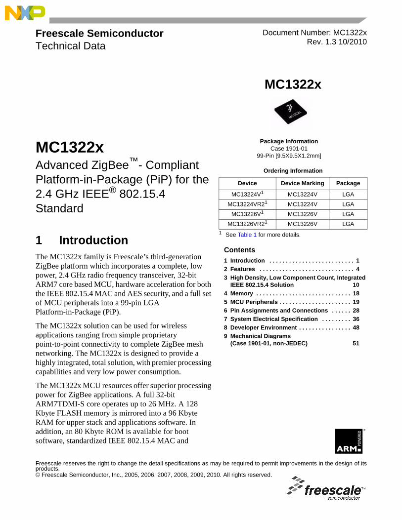
Package InformationCase 1901-01
99-Pin [9.5X9.5X1.2mm]
Ordering Information
Device Device Marking Package
MC13224V1 MC13224V LGA
MC13224VR21 MC13224V LGA
MC13226V1 MC13226V LGA
MC13226VR21 MC13226V LGA1 See Table 1 for more details.1 Introduction
The MC1322x family is Freescale’s third-generation ZigBee platform which incorporates a complete, low power, 2.4 GHz radio frequency transceiver, 32-bit ARM7 core based MCU, hardware acceleration for both the IEEE 802.15.4 MAC and AES security, and a full set of MCU peripherals into a 99-pin LGA Platform-in-Package (PiP).
The MC1322x solution can be used for wireless applications ranging from simple proprietary point-to-point connectivity to complete ZigBee mesh networking. The MC1322x is designed to provide a highly integrated, total solution, with premier processing capabilities and very low power consumption.
The MC1322x MCU resources offer superior processing power for ZigBee applications. A full 32-bit ARM7TDMI-S core operates up to 26 MHz. A 128 Kbyte FLASH memory is mirrored into a 96 Kbyte RAM for upper stack and applications software. In addition, an 80 Kbyte ROM is available for boot software, standardized IEEE 802.15.4 MAC and
MC1322xAdvanced ZigBee™- Compliant Platform-in-Package (PiP) for the 2.4 GHz IEEE® 802.15.4 Standard
Contents1 Introduction . . . . . . . . . . . . . . . . . . . . . . . . . . 12 Features . . . . . . . . . . . . . . . . . . . . . . . . . . . . . 43 High Density, Low Component Count, Integrated
IEEE 802.15.4 Solution 104 Memory . . . . . . . . . . . . . . . . . . . . . . . . . . . . . 185 MCU Peripherals . . . . . . . . . . . . . . . . . . . . . . 196 Pin Assignments and Connections . . . . . . 287 System Electrical Specification . . . . . . . . . 368 Developer Environment . . . . . . . . . . . . . . . . 489 Mechanical Diagrams
(Case 1901-01, non-JEDEC) 51

MC1322x Technical Data, Rev. 1.3
2 Freescale Semiconductor
communications stack software. A full set of peripherals and Direct Memory Access (DMA) capability for transceiver packet data complement the processor core.
The RF radio interface provides for low cost and the high density as shown in Figure 1. An onboard balun along with a TX/RX switch allows direct connection to a single-ended 50-Ω antenna. The integrated PA provides programmable output power typically from -30 dBm to +4 dBm, and the RX LNA provides -96 dBm sensitivity. In addition, separate complementary PA outputs allow use of an external PA and/or an external LNA for extended range applications. The device also has onboard bypass capacitors and crystal load capacitors for the smallest footprint in the industry. All components are integrated into the package except the crystal and antenna.
Figure 1. MC1322x RF Radio Interface
In addition to the best-in-class MCU performance and power, the MC1322x also provides best-in-class power savings. Typical transmit current is 29 mA and typical receive current is 22 mA with the CPU at 2 MHz operation and even lower with the bus stealing enabled. Onboard power supply regulation is provided for source voltages from 2.0 Vdc to 3.6 Vdc. Numerous low current modes are available to maximize battery life including sleep or restricted performance operation.
Applications include, but are not limited to, the following:• Residential and commercial automation
— Lighting control— Security— Access control— Heating, ventilation, air-conditioning (HVAC)— Automated meter reading (AMR)
• Industrial Control
ANALOGTRANSMITTER
ANALOGRECEIVER
RFTX/RX
SWITCHBALUN
LNA
PA
MC1322x Technical Data, Rev. 1.3
Freescale Semiconductor 3
— Asset tracking and monitoring— Homeland security— Process management— Environmental monitoring and control— HVAC— Automated meter reading
• Health Care— Patient monitoring— Fitness monitoring
• Consumer— Remote control— Entertainment systems— Cellular phone attach
1.1 Available DevicesThe MC1322x family is available as two part numbers. These device types differ only in their ROM contents, all other device hardware, performance, and specifications are identical:
• MC13224V - this is the original version and is the generic part type.— The MC13224V is intended for most IEEE 802.15.4 applications including MAC-based,
ZigBee-2007 Profile 1, and ZigBee RF4CE targets.— It has a more complete set of peripheral drivers in ROM.
• MC13226V - this is a more recent version and is provided specifically for ZigBee-2007 Profile 2 (Pro) applications. Only the onboard ROM image has been changed to optimize ROM usage for the ZigBee Pro profile and maximize the amount of available RAM for application use.— The IEEE MAC/PHY functionality has been streamlined to include only that functionality
required by the ZigBee specification. The MAC functionality is 802.15.4 compatible.— For a typical application, up to 20 kbytes more of RAM is available versus the M13224V— Some drivers present in the MC13224 ROM have been removed and these include the ADC,
LCDfont, and SSI drivers. These drivers are still available as library functions, but now compile into the RAM space.
— The Low Level Component (LLC) functionality has also been streamlined for the ZigBee specification
NOTE• When running the Freescale IEEE 802.15.4 MAC (or a related stack) on
the MC1322x platform, neither beaconing or GTS are supported.• See the MC1322x Reference Manual (Document No MC1322xRM), for
information on using applications on these devices.
MC1322x Technical Data, Rev. 1.3
4 Freescale Semiconductor
1.2 Ordering InformationTable 1 provides additional details about the MC1322x
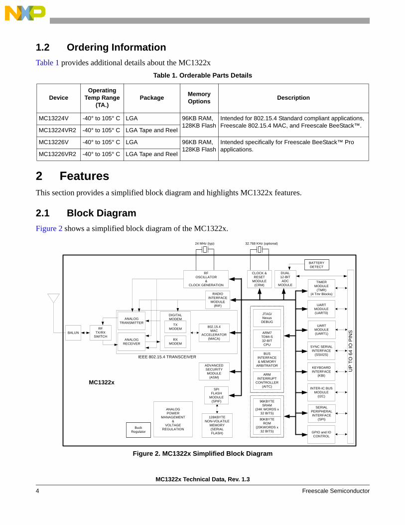
2 FeaturesThis section provides a simplified block diagram and highlights MC1322x features.
2.1 Block DiagramFigure 2 shows a simplified block diagram of the MC1322x.
Figure 2. MC1322x Simplified Block Diagram
Table 1. Orderable Parts Details
Device Operating
Temp Range (TA.)
Package Memory Options Description
MC13224V -40° to 105° C LGA 96KB RAM, 128KB Flash
Intended for 802.15.4 Standard compliant applications, Freescale 802.15.4 MAC, and Freescale BeeStack™.
MC13224VR2 -40° to 105° C LGA Tape and Reel
MC13226V -40° to 105° C LGA 96KB RAM, 128KB Flash
Intended specifically for Freescale BeeStack™ Pro applications.
MC13226VR2 -40° to 105° C LGA Tape and Reel
TIMERMODULE
(TMR)(4 Tmr Blocks)
UARTMODULE(UART0)
UARTMODULE(UART1)
SYNC SERIALINTERFACE
(SSI/i2S)
KEYBOARDINTERFACE
(KBI)
INTER-IC BUSMODULE
(I2C)
SERIALPERIPHERALINTERFACE
(SPI)
DUAL12-BITADC
MODULE
GPIO and IOCONTROL
UP
TO 6
4 IO
PIN
SARM7TDMI-S32-BITCPU
BUSINTERFACE& MEMORY
ARBITRATOR
ARMINTERRUPT
CONTROLLER(AITC)
JTAG/Nexus
DEBUG
ADVANCEDSECURITYMODULE
(ASM)
CLOCK &RESET
MODULE(CRM)
RADIOINTERFACE
MODULE(RIF)
96KBYTESRAM
(24K WORDS x 32 BITS)
80KBYTEROM
(20KWORDS x 32 BITS)
RFOSCILLATOR
&CLOCK GENERATION
SPIFLASH
MODULE(SPIF)
802.15.4MAC
ACCELERATOR(MACA)
DIGITALMODEM
TXMODEM
RXMODEM
128KBYTENON-VOLATILE
MEMORY(SERIALFLASH)
ANALOGTRANSMITTER
ANALOGRECEIVER
RFTX/RX
SWITCH
IEEE 802.15.4 TRANSCEIVER
BALUN
ANALOGPOWER
MANAGEMENT&
VOLTAGEREGULATION
MC1322x
BuckRegulator
24 MHz (typ) 32.768 KHz (optional)
BATTERYDETECT

MC1322x Technical Data, Rev. 1.3
Freescale Semiconductor 5
2.2 Features Summary• IEEE 802.15.4 standard compliant on-chip transceiver/modem
— 2.4 GHz ISM Band operation— 16 selectable channels— Programmable transmitter output power (-30 dBm to +4 dBm typical)— World-class receiver sensitivity
– < -96 dBm typical receiver sensitivity using DCD mode (<1% PER, 20-byte packets)– < -100 dBm typical receiver sensitivity using NCD mode (<1% PER, 20-byte packets)
• Hardware acceleration for IEEE 802.15.4 applications— MAC accelerator (sequencer and DMA interface)— Advanced encryption/decryption hardware engine (AES 128-bit)
• Supports standard IEEE 802.15.4 signaling with 250 kbps data rate• 32-bit ARM7TDMI-S CPU core with programmable performance up to 26 MHz (24 MHz typical)• Extensive on-board memory resources
— 128 Kbyte serial FLASH memory (will be mirrored into RAM)— 96 Kbyte SRAM— 80 Kbyte ROM
• Best-in-class power dissipation— 22 mA typical RX current draw (DCD mode) with radio and MCU active— 29 mA typical TX current draw with radio and MCU active (coin cell capable)— 3.3 mA typical current draw with MCU active (radio off)— 0.8 mA typical current with MCU idle (radio off)— 0.85 μA typical Hibernate current (retain 8 Kbyte SRAM contents)— 0.4 μA maximum Off current (device in reset)
• Extensive sleep mode control and variation— Hibernate and Doze low power modes— Programmable degree of power down— Clock management— Onboard 2 kHz oscillator for wake-up timer.— Optional 32.768 kHz crystal oscillator for accurate real-time sleep mode timing and wake-up
with a possible sleep period greater than 36.4 hours— Wake-up through programmable timer, external real-time interrupts, or ADC timer
• Extensive MCU peripherals set— Dedicated 802.15.4 modem/radio interface module (RIF)— Dedicated NVM SPI interface for managing FLASH memory— Two dedicated UART modules capable of 2 Mbps with CTS/RTS support— SPI port with programmable master and slave operation
MC1322x Technical Data, Rev. 1.3
6 Freescale Semiconductor
— 8-pin keyboard interface (KBI) supports up to a 4x4 matrix. Also, provides up to four asynchronous interrupt inputs for wake-up
— Two 12-bit analog-to-digital converters (ADCs) share 8 input channels— Four independent 16-bit timers with PWM capability. These can cascade in combinations up
to 64-bit operation— Inter-integrated circuit (I2C) interface— Synchronous Serial Interface (SSI) with I2S and SPI capability and FIFO data buffering— Up to 64 programmable I/O shared by peripherals and GPIO
• Powerful In-circuit debug and FLASH programming available via on-chip debug ports— JTAG debug port— Nexus extended feature debug port
• System protection features— Low battery detect— Watchdog timer (COP)— Sleep mode timer
• Low external component count— Only antenna needed for single-ended 50-Ω RF interface (balun in package)— Only a single crystal is required for the main oscillator; programmable crystal load capacitors
are on-chip— All bypass capacitors in package
• Supports single crystal reference clock source (typical 24 MHz crystal with 13 - 26 MHz usable) with on-chip programmable crystal load capacitance or external frequency source. Also provides onboard 2 kHz oscillator for wake-up timing or an optional 32.768 kHz crystal for accurate low power timing.
• 2.0 V to 3.6 V operating voltage with on-chip voltage regulators.• Optional buck converter for better battery life.• -40 °C to +105 °C temperature range• RoHS-compliant 9.5mm x 9.5mm x 1.2mm 99-pin LGA package

MC1322x Technical Data, Rev. 1.3
Freescale Semiconductor 7
2.3 Software SolutionsFreescale provides a powerful software environment called the Freescale BeeKit Wireless Connectivity Toolkit. BeeKit is a comprehensive codebase of wireless networking libraries, application templates, and sample applications. The BeeKit Graphical User Interface (GUI), part of the BeeKit Wireless Connectivity Toolkit, allows users to create, modify, and update various wireless networking implementations. A wide range of software functionality is available to complement the MC1322x and these are provided as codebases within BeeKit. The following sections describe the available tools.
NOTEThe MC13226V is intend specifically for use with the BeeStack codebase, see Section 2.3.4.2, “Using BeeStack on the MC1322x Platform”.
2.3.1 Simple Media Access Controller (22xSMAC)The Freescale Simple Media Access Controller (22xSMAC) is a simple ANSI C based code stack available as sample source code. The SMAC can be used for developing proprietary RF transceiver applications using the MC1322x.
• Supports point-to-point and star network configurations• Proprietary networks• Source code and application examples provided
2.3.2 IEEE 802.15.4 2006 Standard-Compatible MACThe Freescale 802.15.4 Standard MAC is a code stack available as object code. The 802.15.4 MAC is used in two ways:
• The 802.15.4 MAC is the heart of all Freescale non-SMAC codebases. All higher level stacks are built on the MAC services
• Customers also use the MAC for developing networking applications based on the full IEEE® 802.15.4 Standard but having custom Network Layer and application services.
NOTEThe basic MAC is fully 802.15.4 compliant on the HCS08 platform; however, on the MC1322x ARM platform, beaconing and GTS are not supported. This has no impact on ZigBee stacks as these do not utilize these features.
Features of the 22x MAC include• Supports star, mesh and cluster tree topologies• Does not support beaconed networks• Does not supports GTS• Multiple power saving modes• AES-128 Security module• 802.15.4 Sequence support

MC1322x Technical Data, Rev. 1.3
8 Freescale Semiconductor
• 802.15.4 Receiver Frame filtering.• Binaries and application examples provided
2.3.3 SynkroRF PlatformThe SynkroRF Network is a general purpose, proprietary networking layer that sits on top of the IEEE® 802.15.4 MAC and PHY layers. It is designed for Wireless Personal Area Networks (WPANs) and conveys information over short distances among the participants in the network. It enables small, power efficient, inexpensive solutions to be implemented for a wide range of applications. Some key characteristics of an SynkroRF Network are:
• An over-the-air data rate of 250 kbit/s in the 2.4 GHz band.• 3 independent communication channels in the 2.4 GHz band (15, 20, and 25).• 2 network node types, controller and controlled nodes.• Channel Agility mechanism.• Low Latency Tx mode automatically enabled in conditions of radio interference.• Fragmented mode transmission and reception, automatically enabled in conditions of radio
interference.• Robustness and ease of use.• Essential functionality to build and support a CE network.
The SynkroRF Network layer uses components from the standard HC(S)08 Freescale platform, which is also used by the Freescale’s implementations of 802.15.4. MAC and ZigBee™ layers. For more details about the platform components, see the Freescale Platform Reference Manual.
2.3.4 ZigBee-Based StacksFreescale has two independent codebases to support the two ZigBee standard specifications:
• BeeStack™ - supports ZigBee-2007 and ZigBee Pro extensions• BeeStack Consumer - supports ZigBee RF4CE
2.3.4.1 BeeStackFreescale’s BeeStack architecture implements the ZigBee-2007 protocol stack including both Stack Profile 1 and Stack Profile 2 (Pro). Based on the OSI Seven-Layer model, the ZigBee stack ensures inter-operability among networked devices. The physical (PHY), media access control (MAC), and network (NWK) layers create the foundation for the application (APL) layers. BeeStack defines additional services to improve the communication between layers of the protocol stack.
At the Application Layer, the application support layer (ASL) facilitates information exchange between the Application Support Sub-Layer (APS) and application objects. Finally, ZigBee Device Objects (ZDO), in addition to other manufacturer-designed applications, allow for a wide range of useful tasks applicable to home and industrial automation.
MC1322x Technical Data, Rev. 1.3
Freescale Semiconductor 9
BeeStack uses the IEEE 802.15.4-compatible MAC/PHY layer that is not part of ZigBee itself. The NWK layer defines routing, network creation and configuration, and device synchronization. The application framework (AF) supports a rich array of services that define ZigBee functionality. ZigBee Device Objects (ZDO) implement application-level services in all nodes via profiles. A security service provider (SSP) is available to the layers that use encryption (NWK and APS), i.e., Advanced Encryption Standard (AES) 128-bit security.
The complete Freescale BeeStack protocol stack includes the following components:• ZigBee Device Objects (ZDO) and ZigBee Device Profile (ZDP)• Application Support Sub-Layer (APS)• Application Framework (AF)• Network (NWK) Layer• Security Service Provider (SSP)• IEEE 802.15.4-compatible MAC and Physical (PHY) Layer
NOTEFor more details on the ZigBee model and protocol, the user is directed to the ZigBee Specification at www.zigbee.org.
In addition to the use of two Stack Profiles, ZigBee also embraces the concept of application profiles. The profiles are intended to assure interoperability between like devices for a specific application from different vendors. The application profile specifies a device description and its messaging protocol such that it defines the type, shape, and features of the network. The ZigBee Alliance defines each profile and targets a specific market. Examples include Smart Energy, Home Automation, Health Care, and Remote Control.
Freescale’s BeeStack supports a number of these application profiles through demonstration software projects. These projects can be used as a starting point for the user to develop their specific application.
For more information on Freescale supported application profiles see AN3403, Freescale IEEE 802.15.4/ZigBee Software Selector Guide.
2.3.4.2 Using BeeStack on the MC1322x PlatformWhen using the BeeStack codebases on the MC1322x platform, the application should be targeted to the proper part number:
• MC13224V should be used for ZigBee Profile 1 applications• MC13226V should be used for ZigBee Profile 2 (Pro) applications
BeeStack for the MC1322x platform is a single codebase, device selection is determined by a configuration wizard when the BeeKit project is first developed.
2.3.4.3 BeeStack ConsumerIn response to significant market opportunity in the consumer electronics remote control market, the ZigBee Alliance adapted the ZigBee RF4CE Specification in 2009. Freescale’s BeeStack Consumer stack implements the ZigBee RF4CE protocol. It is also a networking layer that sits on top of the IEEE®

MC1322x Technical Data, Rev. 1.3
10 Freescale Semiconductor
802.15.4 MAC. It is designed for standards-based Wireless Personal Area Networks (WPANs) of home entertainment products and conveys information over short distances among the participants in the network. It enables small, power efficient, inexpensive solutions to be implemented for a wide range of applications. Targeted applications include DTV, set top box, A/V receivers, DVD players, security, and other consumer products.
Some key characteristics of a BeeStack Consumer network are:• Based on IEEE 802.15.4 Standard• Use 3 of the standard 802.15.4 communication channels in the 2.4 GHz band, namely, Channels
15, 20, and 25• 2 network node types, controller node and target node• Channel Agility mechanism• Provides robustness and ease of use• Includes essential functionality to build and support a CE network• Binaries, and application examples provided
3 High Density, Low Component Count, Integrated IEEE 802.15.4 Solution
The MC1322x is more than a high performance, low power platform-in-a-package IEEE 802.15.4 solution. Not only are the transceiver (radio) and MCU on an SoC, the packaged solution contains a 128 Kbyte serial FLASH memory, onboard bypass capacitors for critical nodes, and RF components that present a single-ended 50-Ω interface for an external antenna. The radio is a full differential design with an on-chip transmit/receive (TX/RX) switch, and the PiP also has an onboard balun for differential to singled-ended conversion. On-chip RF matching is also provided to present the proper impedance to the antenna.
To further simplify the application, single crystal operation (optimized for 24 MHz) is supported for full radio and MCU operation. If the default 24 MHz crystal is not used, the device supports 13-26 MHz crystals also. The load capacitance to the crystal oscillator is supplied on-chip to eliminate the need for the otherwise required external capacitors.
3.1 Integrated IEEE 802.15.4 Transceiver (Radio and Modem)The MC1322x IEEE 802.15.4 fully-compliant transceiver provides a complete 2.4 GHz radio with 250 kbps Offset-Quadrature Phase Shift Keying (O-QPSK) data in 5.0 MHz channels and full spread-spectrum encode and decode. The modem supports transmit, receive, clear channel assessment (CCA), Energy Detect (ED), and Link Quality Indication (LQI) as required by the 802.15.4 Standard.
3.1.1 RF Interface and UsageThe MC1322x RF interface provides for a single-ended, 50-Ω port that connects directly to an antenna. There is an onboard balun that converts the single-ended interface to a full differential, bi-directional, on-chip interface with transmit/receive switch, LNA, and complementary PA outputs. The required port

MC1322x Technical Data, Rev. 1.3
Freescale Semiconductor 11
impedance matching is also onboard. This combination allows for a very small footprint and a very low cost RF solution.
The MC1322x also provides a secondary set of complementary PA outputs that can be used with external RF circuitry such as a additional PA for higher TX power to the antenna. The single-ended port continues as the receive input for this circuit configuration.
The receiver demodulator includes a module called the Differential Chip Detector which has two modes of operation:
• Non-coherent Detection (NCD) with automatic frequency control (AFC)• Non-coherent Differential Chip Detection (DCD) without AFC
The IEEE 802.15.4 standard allows a maximum clock drift of ±40 ppm (which equals ±80 ppm station-to-station). The MC1322x 802.15.4 demodulator includes two different methods of operating in the presence of such large frequency errors:NCD Mode Provides an increased ~3.5 dB of sensitivity. However, the addition of the AFC
increases the demodulator current drain about 3 mA.DCD Mode Default receive mode at lower current.
For longer range applications where external amplification may be desired (LNA and/or PA), additional ports are provided for secondary complementary PA outputs. These can be used as a separate PA interface while the single-ended port through the balun is used as an input only. Also, four control pins and a regulated 20mA voltage source are provided to control external components and supply power to the PA outputs.
The RF Interface functionality can be summarized as follows:• Programmable output power — 0 dBm nominal output power, programmable from -30 to +4 dBm• Receive sensitivity (at 1% PER, 20-byte packet) -
— < -96 dBm (typical) DCD receive (well above IEEE 802.15.4 specification of -85 dBm)— < -100 dBm (typical) NCD receive (higher current)
• Single-ended 50-Ω antenna port — Uses integrated transmit/receive (T/R) switch, LNA, and onboard balun. Impedance matching onboard.
• Maximum flexibility — The optional single-ended port becomes RF input only and a separate set of full differential PA outputs are provided. Separate input and outputs allow for a variety of RF configurations including external LNA and PA for increased range
• Four control signals for external RF components such as a LNA or PA• Regulated voltage source for PA biasing and powering external components
3.1.2 ModemThe modem supports the full requirement of the IEEE 802.15.4 Standard to transmit and receive data packets. In additional, the mechanism is present to measure received signal level to provide CCA, ED, and LQI as required by the 802.15.4 Standard.

MC1322x Technical Data, Rev. 1.3
12 Freescale Semiconductor
3.2 High Performance, Low Power 32-Bit ARM7 Processor• The ARM7TDMI-S processor is a member of the 32-bit ARM family of general-purpose 32-bit
microprocessors that offers high performance with very low-power consumption• A three stage instruction pipeline (fetch, decode, execute) increases the speed of the flow of
instructions to the processor• Data access can be 8-bit bytes, 16-bit half words, or 32-bit words. Words must be aligned to 4-byte
boundaries. Half words must be aligned to 2-byte boundaries• The ARM7TDMI-S processor supports two instruction sets, the 32-bit ARM instruction set and the
16-bit Thumb instruction set. The Thumb mode incorporates 16-bit instructions for higher code density while retaining all the benefits of a 32-bit architecture, such as the full 32-bit registers, 32-bit operations, and 32-bit memory transfer. The use of the instruction sets can be intermixed for maximizing performance while retaining higher code density
Figure 3. ARM7TDMI-S 32-Bit CPU Core
Register Bank31 x 32-Bit Registers(6 Status Registers)
Address Register
AddressIncrementer
Incr
emen
ter B
us
PC
Bus
ADDR[31:0]
32 x 8Multiplier
ALU
Bus
ScanDebugControlBarrel
Shifter
32-Bit Alu
A B
us
Write Data RegisterInstruction PipelineRead Data Register
Thumb Instruction Decoder
WDATA[31:0] RDATA[31:0]
InstructionDecoder
andControlLogic
B B
us
MC1322x Technical Data, Rev. 1.3
Freescale Semiconductor 13
3.3 Low Power Operation and Power ManagementThe MC1322x is inherently a very low power device, but it also has extensive power management and an onboard buck regulator option to maximize battery life.
3.3.1 Operating CurrentThe MC1322x operating currents are a function of operating mode. There are two basic low power modes of Hibernate and Doze, and both have options of how much RAM contents are retained. The difference between Hibernate and Doze is that Doze mode keeps the primary reference oscillator running.
Highest operating current is when the radio is active for transmit or receive. Refer to Section 7.4, “Supply Current Characteristics” for more details and specifications.
3.3.2 Power ManagementThe MC1322x power management is controlled through the Clock and Reset Module (CRM). The CRM is a dedicated module to handle MCU clock, reset, and power management functions which includes control of the power regulators. All these functions have impact on attaining lowest power.
3.3.2.1 CRM FeaturesThe CRM features include:
• Control of system reset• Control clock gating for power savings• Sleep mode (Hibernate and Doze) management
— Degree of chip power down— Retention of programmed parameters— Programmable retention of RAM contents— Clock management
• Wake-up management— Graceful power-up— Clock management— Wake-up via programmable timer or external interrupts.
• Wake-up timer— Hibernate mode - based on onboard 2 kHz oscillator or optional 32.768 kHz crystal oscillator— Doze mode - based on main reference oscillator, typically 24 MHz
• Controls reference clocks based on default 24 MHz crystal oscillator or optional 13-26 MHz oscillator with PLL (external filter) for 24 MHz frequency synthesis.
• MCU watchdog timer (COP)• Software initiated reset• Management control of onboard linear regulators and optional buck regulator
MC1322x Technical Data, Rev. 1.3
14 Freescale Semiconductor
3.3.2.2 CRM OperationThe CRM has primary control of the entire system:
• Reset and power up — After release of the hardware RESETB signal, the CRM will perform a power up sequence of the MCU. The linear regulators and clock sources are managed for a graceful start-up of the MCU and its resources. The radio is not powered until needed
• Normal operation of MCU — The clock management of the MCU and its resources are controlled by the CRM. The processor clock is programmable from low frequencies up to the maximum reference frequency (13-26 MHz optional w/24 MHz standard) to allow the application to trade-off processing speed versus power savings
• Sleep modes and recovery — There are two sleep modes of Hibernate and Doze. The primary difference is that Doze mode keeps the reference oscillator running. Both modes can retain critical programmed parameters and have selectable sizes of RAM retention. Hibernate has lowest power, but Doze allows high accuracy sleep timing. The CRM manages the recovery from low power, similar to power-up from reset, providing regulator and clock management.— Wake-up can be based on external interrupts through 4 KBI inputs— Wake-up can be from internal interrupts— Wake-up can be based on an RTI (wake-up) timer.
• The RTI timer has two possible frequency sources that provide a very low power wake-up option from sleep— One option is an onboard, low accuracy 2 kHz oscillator— A second option is to add an external 32.768 kHz crystal for the RTI clock source— A 32-bit timer allows greater than a 36.4 hour wake-up delay with the 32.768 crystal oscillator
• Other features of the CRM:— An optional COP watchdog timer to monitor CPU program activity— A programmable software reset
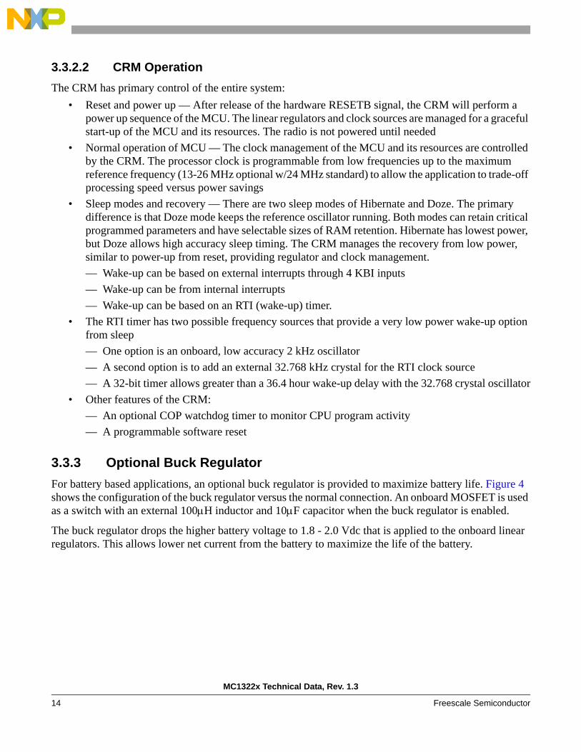
3.3.3 Optional Buck RegulatorFor battery based applications, an optional buck regulator is provided to maximize battery life. Figure 4 shows the configuration of the buck regulator versus the normal connection. An onboard MOSFET is used as a switch with an external 100μH inductor and 10μF capacitor when the buck regulator is enabled.
The buck regulator drops the higher battery voltage to 1.8 - 2.0 Vdc that is applied to the onboard linear regulators. This allows lower net current from the battery to maximize the life of the battery.
MC1322x Technical Data, Rev. 1.3
Freescale Semiconductor 15
Figure 4. Optional Buck Regulator
3.3.4 Battery Voltage MonitorAn optional feature of the ADC module is a battery voltage monitor capability. An onboard 1.2 Vdc reference voltage can be sampled by the ADC module. The battery-sourced supply voltage is used as the high reference voltage for the ADC and as the supply voltage lowers due to battery usage, the onboard reference voltage reading will become greater because this fixed voltage is a higher percentage of the reduced supply voltage.
Programmable high and low thresholds are provided for an ADC analog sample channel to monitor the reference voltage. This feature can be used as a trigger to provide low battery indication, protection for data that may be lost due to end-of-life for the battery, monitoring charging, and controlling buck regulator operation.
3.4 IEEE 802.15.4 Acceleration HardwareThe MC1322x provides acceleration hardware for IEEE 802.15.4 applications and this hardware includes 802.15.4 MAC acceleration and AES encryption/decryption.
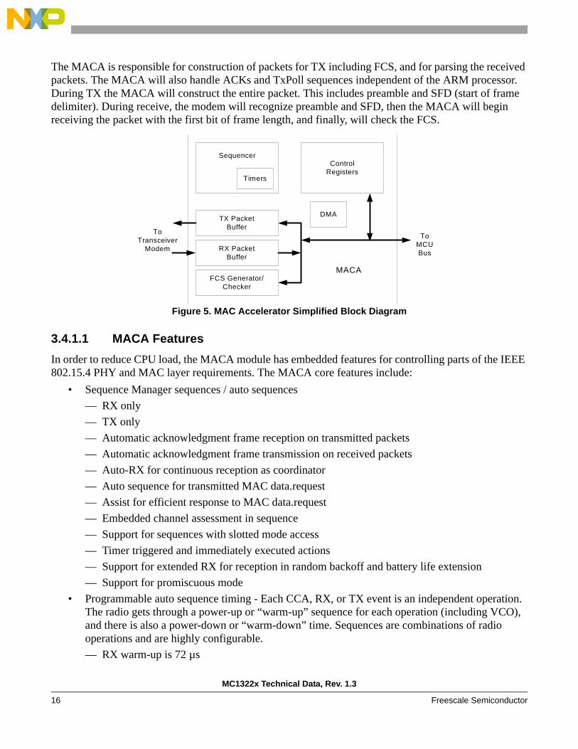
3.4.1 802.15.4 MAC Accelerator (MACA) OverviewThe MC1322x contains a hardware block that provides a low-level MAC and PHY link controller, which together with software running on the ARM core, implements the baseband protocols and other low-level link routine control and link control. Components of the MACA include a sequencer/controller (with timers), TX and RX packet buffers, DMA block, frame check sequence (FCS) generator/checker, and control registers. Figure 5 shows a MACA simplified block diagram.
As part of the 802.15.4 protocol, packets are generated and transmitted, packets are received and verified, and channel energy is measured via a clear channel assessment (CCA). Also, combinations or sequences of events are required as part of the protocol such as an ACK response following a received packet. The MACA facilitates these activities via control of the transceiver and off loads the functions from the CPU. A dedicated DMA function moves data between the MACA buffers and RAM on a cycle steal basis and does not require intervention from the CPU.
VBATT
COIL_BK
LR EG_BK_FB
VDD
NC
LREG_BK_FB
VDD
L2
100uH
C210uF
COIL_BK
VBATT
Normal Operation
D1DIODE SCHOTTKY
Buck Regulator Enabled
MC1322x Technical Data, Rev. 1.3
16 Freescale Semiconductor
The MACA is responsible for construction of packets for TX including FCS, and for parsing the received packets. The MACA will also handle ACKs and TxPoll sequences independent of the ARM processor. During TX the MACA will construct the entire packet. This includes preamble and SFD (start of frame delimiter). During receive, the modem will recognize preamble and SFD, then the MACA will begin receiving the packet with the first bit of frame length, and finally, will check the FCS.
Figure 5. MAC Accelerator Simplified Block Diagram
3.4.1.1 MACA FeaturesIn order to reduce CPU load, the MACA module has embedded features for controlling parts of the IEEE 802.15.4 PHY and MAC layer requirements. The MACA core features include:
• Sequence Manager sequences / auto sequences— RX only— TX only— Automatic acknowledgment frame reception on transmitted packets— Automatic acknowledgment frame transmission on received packets— Auto-RX for continuous reception as coordinator— Auto sequence for transmitted MAC data.request— Assist for efficient response to MAC data.request— Embedded channel assessment in sequence— Support for sequences with slotted mode access— Timer triggered and immediately executed actions— Support for extended RX for reception in random backoff and battery life extension— Support for promiscuous mode
• Programmable auto sequence timing - Each CCA, RX, or TX event is an independent operation. The radio gets through a power-up or “warm-up” sequence for each operation (including VCO), and there is also a power-down or “warm-down” time. Sequences are combinations of radio operations and are highly configurable.— RX warm-up is 72 µs
TX PacketBuffer
RX PacketBuffer
Sequencer
Timers
FCS Generator/Checker
DMA
ControlRegisters
MACA
To Transceiver
Modem
ToMCUBus
MC1322x Technical Data, Rev. 1.3
Freescale Semiconductor 17
— TX warm-up is 92 µs— Turnaround times
– The IEEE 802.15.4 Standard requires a TX-to-RX or a RX-to-TX turnaround time to be less than or equal to 12 symbols times (192 µs).
– Best practice for maximum station-to-station performance is to minimize TX-to-RX turnaround time and to maximize (within spec) RX-to-TX turnaround time.
– Auto sequences should use recommended turnaround times of:a) 11 symbols times (176 µs) RX-to-TXb) 96 µs TX-to-RX.
• Dedicated DMA for transfer of TX/RX data from/to RAM (minimum bus clock of 2 MHz for 802.15.4 modem operation)
• Maskable, event-driven interrupt generation• Address header filtering for received packets. A promiscuous mode allows bypass of the filtering
for monitoring network traffic• Packet manager
— Handles preamble data— Handles frame check sequence (FCS) a.k.a CRC— Embedded header filter for received packets
• Control/status registers mapped into CPU memory map• 32-Bit random number generator — Runs at the bus clock rate, a 32-bit Linear Feedback Shift
Register (LFSR) can be set with a seed value and uses a 32-bit primitive polynomial. A 32-bit random number is fetched with every read of the proper control register
3.4.2 Advanced Security Module (ASM)The IEEE 802.15.4 Standard and the ZigBee Standard both provide for optional use of data encryption.The ASM engine is a hardware block that accelerates encryption/decryption using the Advanced Encryption Standard (AES). The engine can perform “Counter” (CTR) and Cipher Block Chaining (CBC) encryption. The combination of these two modes of encryption are known as CCM mode encryption. CCM is short for Counter with CBC-MAC. CCM is a generic authenticate and encrypt block cipher mode. CCM is only defined for use with 128 bit block ciphers, such as AES. The definition of CCM mode encryption is documented in the NIST publication SP800-38C.
The ASM has the following features:• 32-Bit wide bus interface• CTR encryption in 13 clock cycles• CBC encryption in 13 clock cycles• Encrypts 128 bits as a unit• The 128-bit registers are aligned on quad word boundaries (16 byte)• Self-test mode• Maskable “action complete” interrupt
MC1322x Technical Data, Rev. 1.3
18 Freescale Semiconductor
4 MemoryThe MC1322x memory resources consist of RAM, ROM, and serial FLASH.
4.1 RAM and ROMThe RAM and ROM features include:
• 96 Kbytes RAM.— RAM0: 8 Kbytes, 2 Kwords (2048 x 32 bits)— RAM1: 24 Kbytes, 6 Kwords (6144 x 32 bits)— RAM2: 32 Kbytes, 8 Kwords (8192 x 32 bits)— RAM3: 32 Kbytes, 8 Kwords (8192 x 32 bits)
• All read or write accesses require a minimum of two system clock cycles• Stall signal generated for read after write cycles• Clock is enabled only on the accessed memory device for low power consumption• RAMs have been divided to allow for power savings. While sleeping, the above RAM blocks can
be turned off (combinations include 8, 32, 64, and 96 Kbytes active) and the RAM remainder can be placed in a low voltage mode for data retention. If more RAMs are turned on, then less battery life will be achieved. Depending on the amount of RAM powered during sleep, the boot time may be longer with less RAM as the non-powered RAM must be reloaded from FLASH.
• 80 Kbytes ROM— 20 Kwords (20480 x 32 bits)— Initially contains bootstrap code, 802.15.4 MAC and drivers. The MAC software builds on the
lower level hardware capability of the transceiver and MACA. All code except the bootstrap is “patchable”.
4.2 Serial FLASH (NVM)The MC1322x also contains a 128 Kbyte serial FLASH memory that can be mirrored into the 96 Kbyte RAM. The serial FLASH is accessed via an internal dedicated SPI module (SPIF). The FLASH erase, program, and read capability are programmed through the SPIF port. The FLASH is accessed at boot time to load/initialize RAM. All actual CPU program and data access is from RAM or ROM.

MC1322x Technical Data, Rev. 1.3
Freescale Semiconductor 19
5 MCU PeripheralsThe MC1322x has a rich set of MCU peripherals. Figure 6 shows the peripheral modules.
Figure 6. MCU Peripherals
T IM E RM O D U L E
(T M R )(4 T m r B lo c k s )
U A R TM O D U L E(U A R T 0 )
U A R TM O D U L E(U A R T 1 )
S Y N C S E R IA LIN T E R F A C E
(S S I/ i2 S )
K E Y B O A R DIN T E R F A C E
(K B I)
IN T E R -IC B U SM O D U L E
(I2 C )
S E R IA LP E R IP H E R A LIN T E R F A C E
(S P I)
D U A L1 2 -B IT
A D CM O D U L E
G P IO a n d IOC O N T R O L
UP
TO
64
IO P
INSA R M 7
T D M I-S3 2 -B IT
C P U
B U SIN T E R F A C E& M E M O R Y
A R B IT R A T O R
A R MIN T E R R U P T
C O N T R O L L E R(A IT C )
J T A G /N e xu s
D E B U G
F ro mC R M
B A T T E R YD E T E C T
S P IF L A S H
M O D U L E(S P IF )
MC1322x Technical Data, Rev. 1.3
20 Freescale Semiconductor
5.1 Parallel IO (GPIO)The parallel I/O features include:
• A total of 64 general-purpose I/O pins• Individual control (direction and output state) for each pin when in GPIO mode• Pad hysteresis enables• Software-controlled pull-ups/pull-downs on each input pin• When not used as GPIO, the IO provide alternative functions
— Debug ports for JTAG (four signals) and Nexus (fourteen signals) modules— Four control signals for external RF components such as an LNA, PA, and antenna switch— Eight analog inputs for ADC input channels— Four signals for ADC reference voltages— Eight signals for UART1 and UART2— Two I2C signals— Four timer block signals— Four SPI block signals— Four SSI block signals— Eight KBI signals
• Eight KBI pins are kept alive during Hibernate or Doze. Four KBI are output and four are inputs. The input can be used as wake-up interrupts
5.2 Keyboard Interface (KBI)The MC1322x designates 8 pins (KBI_0 to KBI_7) as a keyboard interface, where four of these signals typically are outputs and four are inputs (KBI_4 to KBI_7) that support interrupts. These 8 pins could typically be used as a matrix interface to support up to 16 switches or buttons, such as a keypad. These signals can also be used as general purpose IO if a keyboard is not present.
During Hibernate or Doze, the KBI are unique in that they are kept alive. Four KBI are outputs and four KBI are inputs. The inputs can be enabled as asynchronous interrupts to wake-up the MC1322x from the sleep mode.
MC1322x Technical Data, Rev. 1.3
Freescale Semiconductor 21
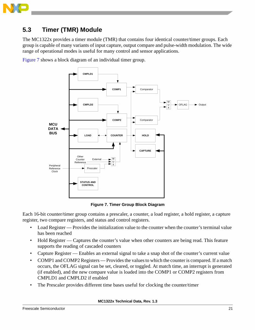
5.3 Timer (TMR) ModuleThe MC1322x provides a timer module (TMR) that contains four identical counter/timer groups. Each group is capable of many variants of input capture, output compare and pulse-width modulation. The wide range of operational modes is useful for many control and sensor applications.
Figure 7 shows a block diagram of an individual timer group.
Figure 7. Timer Group Block Diagram
Each 16-bit counter/timer group contains a prescaler, a counter, a load register, a hold register, a capture register, two compare registers, and status and control registers.
• Load Register — Provides the initialization value to the counter when the counter’s terminal value has been reached
• Hold Register — Captures the counter’s value when other counters are being read. This feature supports the reading of cascaded counters
• Capture Register — Enables an external signal to take a snap shot of the counter’s current value• COMP1 and COMP2 Registers — Provides the values to which the counter is compared. If a match
occurs, the OFLAG signal can be set, cleared, or toggled. At match time, an interrupt is generated (if enabled), and the new compare value is loaded into the COMP1 or COMP2 registers from CMPLD1 and CMPLD2 if enabled
• The Prescaler provides different time bases useful for clocking the counter/timer
CMPLD1
COMP1
LOAD HOLD
STATUS ANDCONTROL
CMPLD2
COMP2
COUNTER
Comparator
Comparator
CAPTURE
MUX
Prescaler
MUX
PeripheralReference
Clock
OtherCounter
Reference
OFLAG Output
External
MCUDATABUS
MC1322x Technical Data, Rev. 1.3
22 Freescale Semiconductor
• The Counter provides the ability to count internal or external events• Control and Status Registers — Provides operational mode control of the counter, status, clock
source control, interrupt control, and external interface control
Four GPIO pins (TMR0 -TMR3) are programmable and can be used with any counter/timer group.
The TMR module feature include:• Four 16-bit counters/timers groups• Up/down count• Counters are cascadable for up to 64-bit delay counter• Programmable count modulo.• Peripheral reference clock is same as bus clock• External clock max count rate equals peripheral clock divided by 2• Internal clock max count rate equals peripheral clock.• Count once or repeatedly• Counters are preloadable• Compare registers are preloadable• Counters share available four GPIO pins (programmable as inputs or outputs and programmable
for falling or rising edge)• Separate prescaler for each counter• Each counter has capture and compare capability• Optional input glitch filter• Functional modes include stop, count, edge-count, gated-count, quadrature-count, signed-count,
triggered-count, one-shot, cascade-count, pulse-output, fixed frequency PWM, and variable-frequency PWM
5.4 UART ModulesThe MC1322x has two universal asynchronous receiver/transmitter (UART) modules. Each UART has an independent fractional divider, baud rate generator that is clocked by the peripheral bus clock (typically 24 MHz) which enables a broad range of baud rates up to 1,843.2 kbaud. Transmit and receive use a common baud rate for each module.
Each UART provides the following features:• 8-bit only data• One or two stop bits• Programmable parity (even, odd, and none)• Full duplex four-wire serial interface (RXD, TXD, RTS, and CTS)• Hardware flow control support for RTS and CTS signals• 32-byte receive FIFO and 32-byte transmit FIFO• Programmable sense for RTS/CTS pins (high true/low true)

MC1322x Technical Data, Rev. 1.3
Freescale Semiconductor 23
• Status flags for various flow control and FIFO states• Receiver detects framing errors, start bit error, break characters, parity errors, and overrun errors.• Voting logic for improved noise immunity (16X/8X oversampling)• Maskable interrupt request• Time-out counter, which times out after eight non-present characters• Receiver and transmitter enable/disable• Low-power modes• Baud rate generator to provide any multiple-of-2 baud rate between 1.2 kbaud and 1,843.2 kbaud
5.5 Inter-Integrated Circuit (I2C) ModuleThe MC1322x provides an Inter-Integrated Circuit (I2C) module for the I2C which is a two-wire, serial data (SDA) and serial clock (SCL), bidirectional serial bus. The I2C allows for data exchange between the MC1322x and other devices such as MCUs, serial EEPROM, serial ADC and DAC devices, and LCDs. The I2C minimizes interconnections between devices and is a synchronous, multi-master bus that allows additional devices to be connected and still handle system expansion and development. The bus includes collision detection and arbitration to prevent data corruption if two or more masters attempt to simultaneously control the I2C.
The I2C module is driven by the peripheral bus clock (typically 24 MHz) and the SCL bit clock is generated from a prescaler. The prescaler divide ratio can be programmed from 61,440 to 160 (decimal) which gives a maximum bit clock of 150 kbps.
The I2C module supports the following features:• Two-wire (SDA and SCL) interface• Multi-master operation• Master or slave mode• Arbitration lost interrupt with automatic mode switching from master to slave• Calling address identification interrupt• START and STOP signal generation/detection• Acknowledge bit generation/detection• Bus busy detection• Software-programmable bit clock frequency up to 150 kbps• Software-selectable acknowledge bit• On-chip filtering for spikes on the bus

MC1322x Technical Data, Rev. 1.3
24 Freescale Semiconductor
5.6 Serial Peripheral Interface (SPI) ModulesThe MC1322x has two SPI modules that use a common architecture
5.6.1 External SPI ModuleThe MC1322x offers a dedicated Serial Peripheral Interface (SPI) module for external use. The SPI is a high-speed synchronous serial data input/output port used for interfacing with serial memories, peripheral devices, or other processors. The SPI allows a serial bit stream of a programmed length (1 to 32 bits) to be shifted simultaneously into and out of the device at a programmed bit-transfer rate (called 4-wire mode). There are four pins associated with the SPI port (SPI_SCK, SPI_MOSI, SPI_MISO, and SPI_SS).
The SPI module can be programmed for master or slave operation. It also supports a 3-wire mode where for master mode the MOSI becomes MOMI, a bidirectional data pin, and for slave mode the MISO becomes SISO, a bidirectional data pin. In 3-wire mode, data is only transferred in one direction at a time.
The SPI bit clock is derived from the peripheral reference clock (typically 24 MHz with a maximum of 26 MHz). A prescaler divides the peripheral reference clock with a programmed divide ratio from 2 to 256. Typical bit clock range will be from 12 MHz to 93.75 kHz.
The SPI has the following features:• Master or slave mode operation• Data buffer is 4 bytes (32 bits) in length• SPI transfer length programmable from 1 to 32 bits• MSB-first shifting• Programmable transmit bit rate (typically 12 MHz max)• Serial clock phase and polarity options• Full-duplex (4-wire) or bidirectional data (3-wire) operation• SPI transaction can be polled or interrupt driven• Slave select signal• Low Power (SPI Master uses gated clocks. SPI Slave clock derived completely from SPI_SCK.)
5.6.2 SPI FLASH Module (SPIF)The SPIF is an internal SPI block dedicated to control, reading, and writing of the serial FLASH memory (NVM). It uses the same architecture as the general SPI block, but is limited by the characteristics of the FLASH SPI interface.
MC1322x Technical Data, Rev. 1.3
Freescale Semiconductor 25
5.7 Synchronous Serial Interface (SSI) ModuleThe MC1322x provides a versatile Synchronous Serial Interface (SSI) which is a full-duplex, serial port that allows communication with a variety of serial devices. These serial devices can be digital signal processors (DSPs), MCUs, peripherals, popular industry audio CODECs, and devices that implement the Inter-Integrated Circuit sound bus standard (I2S).
The SSI typically transfers samples in a periodic manner and it consists of independent transmitter and receiver sections with common clock generation and frame synchronization. The external signals include the bit clock (SSI_BITCK), frame sync (SSI_FSYN), RX data (SSI_RX), and TX data (SSI_TX). The SSI has the following basic operating modes all with synchronous protocol:
• Normal mode — The simplest SSI mode transfers data in one time slot per frame• Network mode — Creates a Time Division Multiplexed (TDM) network, such as a TDM CODEC
network or a network of DSPs• Gated Clock mode — Connects to SPI-type interfaces on MCUs or external peripheral chips
With its multi-modes, the SSI can be programmed for two very useful functions:• A second SPI port augmenting the MC1322x SPI module• I2S interface - the SSI is capable of generating the required clock frequencies and data format to
drive a serial stereo audio DAC
The SSI includes the following features:• Synchronous transmit and receive sections with shared internal/external clocks and frame syncs,
operating in Master or Slave mode.• Normal mode operation using frame sync• Network mode operation allowing multiple devices to share the port with as many as thirty-two
time slots• Gated Clock mode operation requiring no frame sync• SSI clock source is Peripheral Clock (typically 24 MHz); maximum SSI transfer rate is 6.0 MHz• Separate Transmit and Receive FIFOs. Each of which is 8x24 bits• Programmable data interface modes including I2S, LSB, MSB aligned• Programmable word length (8, 10, 12, 16, 18, 20, 22 or 24 bits)• Program options for frame sync and clock generation• Programmable I2S modes (Master, Slave)• Programmable internal clock divider• Time Slot Mask Registers for reduced CPU overhead (for Tx and Rx both)• SSI power-down feature

MC1322x Technical Data, Rev. 1.3
26 Freescale Semiconductor
5.8 Analog-to-Digital Converter (ADC) Module
The MC1322x ADC module provides two 12-bit analog-to-digital converters (ADC_1 and ADC_2) with eight external channels (ADC7 - ADC0) that can be multiplexed to either ADC. ADC_1 can also sample a battery reference voltage for monitoring purposes. External pins (ADC2_VREFH, ADC2_VREFL, ADC1_VREFH, and ADC1_VREFL) are provided for independent ADC reference voltages. The minimum sample time is 20 µs. Figure 8 shows a block diagram of the ADC module.
Each ADC can be programmed to scan multiple selected channels on a timed basis. The primary clock to the ADC module is the peripheral reference clock (typically 24 MHz). For the time period between scan sequences, the primary clock is first divided by an 8-bit prescale (1-255), and the derived clock drives both the 32-bit delay timer and the ADC sequencer. Each ADC has its own delay timer and sequencer.
Once a scan sequence has been initiated, all selected channels can be sampled. Registers are provided to define thresholds that can be enabled for the sampled channels. A threshold can be assigned to a specific channel and can be programmed to be a less-than or greater-than threshold. Multiple thresholds can be assigned to a single channel. Warm-up of the analog portion of the ADC circuitry is provided for power management, and a separate 300 kHz ADC clock must be programmed via its own divider.
The battery monitor has two (2) dedicated threshold registers to set the high and low limits of the battery sample channel.
Sample values are stored in a 8x16-bit FIFO. The FIFO accumulates samples from both ADCs, and the 12-bit sample value and a 4-bit channel tag are saved for each sample. The FIFO is read by the CPU from a register address.
The module can be programmed to interrupt the processor based on the timed sample activity. Sample activity, sequencer activity, or FIFO “fullness” can all be enabled to generate an interrupt.
The ADCs can also be overridden to sample on command as opposed to sequencer, time-based activity.
Figure 8. ADC Module Block Diagram
MUX
MUX
Analog ChannelsADC0 - ADC7
Battery
ADC_1
ADC_2
FIFO(8 x 16-Bit,
12-bit value + 4-
bit channelTag)
ControlRegisters
Divider
MUX
ControlOverride
Mode
Sequencer2
MUX
ControlOverride
Mode
Sequencer1
Com pare
MCUDATABUS
PrescalerAnalog
ADC2 Mux Sel
ADC1 Mux Sel
ADC1 Enable
ADC2 Enable
AD
C C
lock
AD
C C
lock
32-BitTimer
32-BitTim er
PeripheralReference C lock
300 kHz
MC1322x Technical Data, Rev. 1.3
Freescale Semiconductor 27
The ADC module has the following features:• 12 bit resolution. Effective number of bits 8-9• Valid usable input voltage range: [Vref_high-0.2V] to [Vref_low+0.2V]• Maximum input range: VBATT to VSS• Minimum sample time 20 µs• Peripheral Clock (set by CRM) uses an 8-bit prescaler to provide the time base for the module• Two independent channels, each with a 32-bit timer• ADC_1 has 9 channels: 8 external analog inputs plus battery reference voltage• ADC_2 has 8 channels: 8 external analog inputs• Active channels for each ADC are programmable• Eight active monitors plus battery reference monitors can generate a IRQ• An 8-deep FIFO for recording data• IRQs can be generated by the channel compare values, FIFO status, and sequencers

MC1322x Technical Data, Rev. 1.3
28 Freescale Semiconductor
6 Pin Assignments and Connections
Figure 9. MC1322x Pinout (Top View: Bottom Pads Shown)
Notes:1. Bottom pads 75-79, 84-88, 93-97, 104-106, and 115 are Substrate Ground.
3. All remaining bottom pads are isolated from ground (NC), and are provided here for mechanical strength.4. Figure 15 (Mechanical Diagram), is the bottom view, not the top view as shown here.
1
2
3
4
5
6
7
8
9
10
11
12
13
14
15
1617 18 19 20 21 22 23 24 25 26 27 28 29 30 31 32
33
34
35
36
37
38
39
40
41
42
43
44
45
46
47
48495051525354555657585960616263
64
ADC1ADC0
ADC3ADC2
ADC5ADC4
ADC7_RTCKADC6
TDITDO
TMSTCK
UART2_CTSUART2_RTS
UART2_TXUART2_RX
XTAL_32_INXTAL_32_OUT
VBATTRF_PLL_FLT
COIL_BKLREG_BK_FB
KBI_1KBI_0_HST_WK
KBI_3KBI_2
KBI_5KBI_4
KBI_7KBI_6
SSI_RXSSI_TX
UA
RT1
_RTS
UA
RT1
_CTS
UA
RT1
_RX
UA
RT1
_TX
I2C
_SD
AI2
C_S
CL
TMR
3TM
R2
TMR
1TM
R0
SPI_
SCK
SPI_
MO
SISP
I_M
ISO
SPI_
SSSS
I_B
ITC
KSS
I_FS
YN
PA_P
OS
PA_N
EGTX
_ON
RES
ETB
XTA
L_24
_IN
XTA
L_24
_OU
T
RF_
RX_
TXR
X_O
NR
F_G
ND
AN
T_2
AN
T_1
RF_
BIA
S
AD
C2_
VREF
HA
DC
1_VR
EFH
AD
C1_
VREF
LA
DC
2_VE
RFL
Substrate GND Pads
102
75 76
103
111 112 113 114
120 121 122 124
129 130 131 133
123
132
77 78 79
84 85 86 87 88
93 94 95 96 97
104 105 106
115
66 67 68 69 70 71 72 7365
74
83
92
101
110
119
128
137 138 139 140 141 142 143 144 145
80
89
98
107
116
125
134
81
90
98
108
117
126
135
82
91
100
109
118
127
136
MC1322x
Active Signal Pads
2. Bottom pads 102-103, 111-114, 120-124, and 129-133 are active pads.
MC1322x Technical Data, Rev. 1.3
Freescale Semiconductor 29
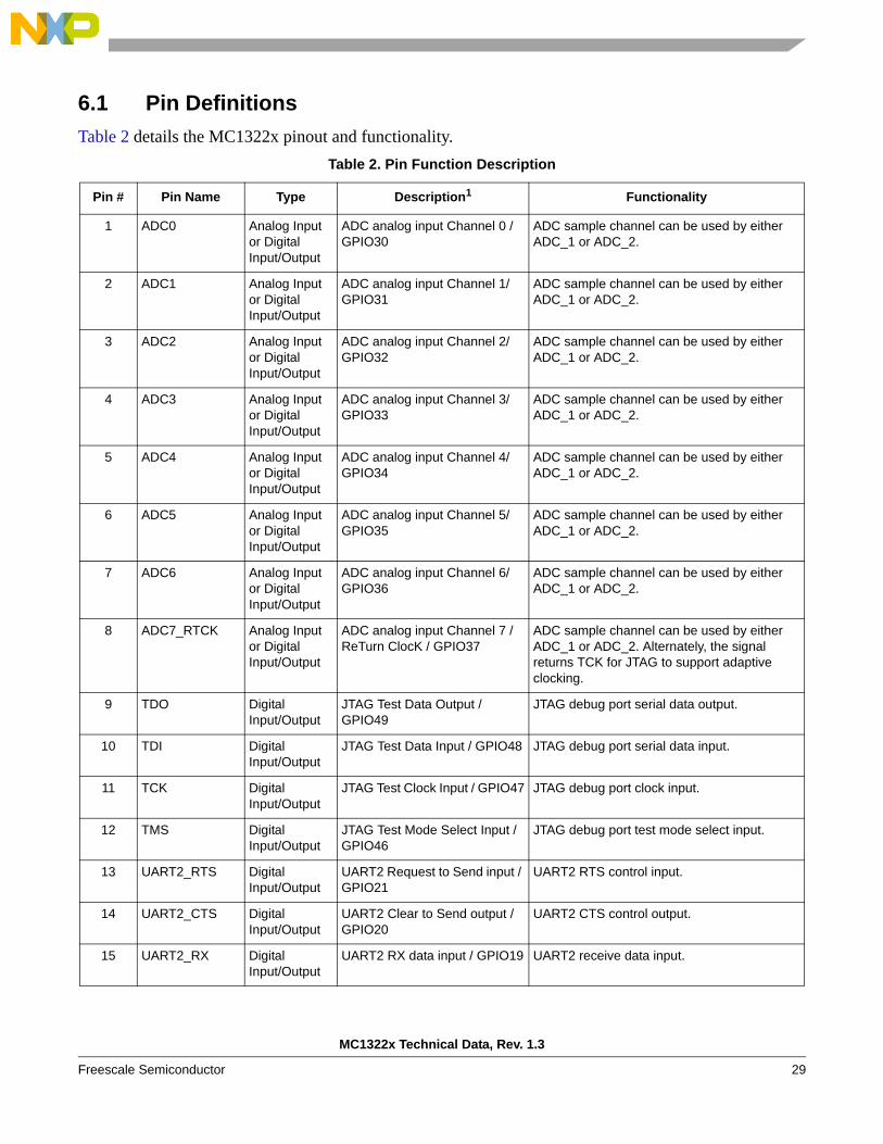
6.1 Pin DefinitionsTable 2 details the MC1322x pinout and functionality.
Table 2. Pin Function Description
Pin # Pin Name Type Description1 Functionality
1 ADC0 Analog Input or Digital Input/Output
ADC analog input Channel 0 / GPIO30
ADC sample channel can be used by either ADC_1 or ADC_2.
2 ADC1 Analog Input or Digital Input/Output
ADC analog input Channel 1/ GPIO31
ADC sample channel can be used by either ADC_1 or ADC_2.
3 ADC2 Analog Input or Digital Input/Output
ADC analog input Channel 2/ GPIO32
ADC sample channel can be used by either ADC_1 or ADC_2.
4 ADC3 Analog Input or Digital Input/Output
ADC analog input Channel 3/ GPIO33
ADC sample channel can be used by either ADC_1 or ADC_2.
5 ADC4 Analog Input or Digital Input/Output
ADC analog input Channel 4/ GPIO34
ADC sample channel can be used by either ADC_1 or ADC_2.
6 ADC5 Analog Input or Digital Input/Output
ADC analog input Channel 5/ GPIO35
ADC sample channel can be used by either ADC_1 or ADC_2.
7 ADC6 Analog Input or Digital Input/Output
ADC analog input Channel 6/ GPIO36
ADC sample channel can be used by either ADC_1 or ADC_2.
8 ADC7_RTCK Analog Input or Digital Input/Output
ADC analog input Channel 7 / ReTurn ClocK / GPIO37
ADC sample channel can be used by either ADC_1 or ADC_2. Alternately, the signal returns TCK for JTAG to support adaptive clocking.
9 TDO Digital Input/Output
JTAG Test Data Output / GPIO49
JTAG debug port serial data output.
10 TDI Digital Input/Output
JTAG Test Data Input / GPIO48 JTAG debug port serial data input.
11 TCK Digital Input/Output
JTAG Test Clock Input / GPIO47 JTAG debug port clock input.
12 TMS Digital Input/Output
JTAG Test Mode Select Input / GPIO46
JTAG debug port test mode select input.
13 UART2_RTS Digital Input/Output
UART2 Request to Send input / GPIO21
UART2 RTS control input.
14 UART2_CTS Digital Input/Output
UART2 Clear to Send output / GPIO20
UART2 CTS control output.
15 UART2_RX Digital Input/Output
UART2 RX data input / GPIO19 UART2 receive data input.

MC1322x Technical Data, Rev. 1.3
30 Freescale Semiconductor
16 UART2_TX Digital Input/Output
UART2 TX data output / GPIO18
UART2 transmit data output.
17 UART1_RTS Digital Input/Output
UART1 Request to Send input / GPIO17
UART1 RTS control input.
18 UART1_CTS Digital Input/Output
UART1 Clear to Send output / GPIO16
UART1 CTS control output.
19 UART1_RX Digital Input/Output
UART1 RX data input / GPIO15 UART1 receive data input.
20 UART1_TX Digital Input/Output
UART1 TX data output / GPIO14
UART1 transmit data output.
21 I2C_SDA Digital Input/Output
I2C Bus data / GPIO13 I2C bus signal SDA
22 I2C_SCL Digital Input/Output
I2C Bus clock / GPIO12 I2C bus signal SCL
23 TMR3 Digital Input/Output
Timer 3 IO signal / GPIO11 Pin is used as counter output or counter input clock.
24 TMR2 Digital Input/Output
Timer 2 IO signal / GPIO10 Pin is used as counter output or counter input clock.
25 TMR1 Digital Input/Output
Timer 1 IO signal / GPIO9 Pin is used as counter output or counter input clock.
26 TMR0 Digital Input/Output
Timer 0 IO signal / GPIO8 Pin is used as counter output or counter input clock.
27 SPI_SCK Digital Input/Output
SPI Port clock / GPIO7 SPI port clock.
28 SPI_MOSI Digital Input/Output
SPI Port MOSI/ GPIO6 SPI Port Master Out Slave In (MOSI) data signal.
29 SPI_MISO Digital Input/Output
SPI Port MISO / GPIO5 SPI Port Master In Slave Out (MISO) data signal.
30 SPI_SS Digital Input/Output
SPI Port SS / GPIO4 SPI Port Slave Select (SS) signal.
31 SSI_BITCK Digital Input/Output
SSI Bit Clock / GPIO3 SSI serial TX/RX clock and is bi-directional.
32 SSI_FSYN Digital Input/Output
SSI Frame Sync / GPIO2 SSI frame sync for data (RX or TX) and is bi-directional.
33 SSI_RX Digital Input/Output
SSI RX data input / GPIO1 SSI serial RX data input.
34 SSI_TX Digital Input/Output
SSI TX data output / GPIO0 SSI serial TX data output.
35 KBI_7 Digital Input/Output
Keyboard Interface Bit 7 / GPIO29
Asynchronous interrupt input.
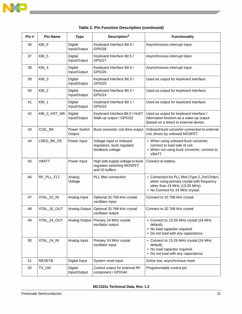
Table 2. Pin Function Description (continued)
Pin # Pin Name Type Description1 Functionality
MC1322x Technical Data, Rev. 1.3
Freescale Semiconductor 31
36 KBI_6 Digital Input/Output
Keyboard Interface Bit 6 / GPIO28
Asynchronous interrupt input.
37 KBI_5 Digital Input/Output
Keyboard Interface Bit 5 / GPIO27
Asynchronous interrupt input.
38 KBI_4 Digital Input/Output
Keyboard Interface Bit 4 / GPIO26
Asynchronous interrupt input.
39 KBI_3 Digital Input/Output
Keyboard Interface Bit 3 / GPIO25
Used as output for keyboard interface.
40 KBI_2 Digital Input/Output
Keyboard Interface Bit 2 / GPIO24
Used as output for keyboard interface.
41 KBI_1 Digital Input/Output
Keyboard Interface Bit 1 / GPIO23
Used as output for keyboard interface.
42 KBI_0_HST_WK Digital Input/Output
Keyboard Interface Bit 0 / HoST Walk-up output / GPIO22
Used as output for keyboard interface / Alternative function as a wake-up output (based on a timer) to external device.
43 COIL_BK Power Switch Output
Buck converter coil drive output Onboard buck converter connection to external coil, driven by onboard MOSFET.
44 LREG_BK_FB Power Input Voltage input to onboard regulators, buck regulator feedback voltage
• When using onboard buck converter, connect to load side of coil.
• When not using buck converter, connect to VBATT.
45 VBATT Power Input High side supply voltage to buck regulator switching MOSFET and IO buffers
Connect to battery.
46 RF_PLL_FLT Analog Voltage
PLL filter connection • Connection for PLL filter (Type 2, 2nd Order) when using primary crystal with frequency other than 24 MHz (13-26 MHz).
• No Connect for 24 MHz crystal.
47 XTAL_32_IN Analog Input Optional 32.768 kHz crystal oscillator input
Connect to 32.768 kHz crystal
48 XTAL_32_OUT Analog Output Optional 32.768 kHz crystal oscillator output
Connect to 32.768 kHz crystal
49 XTAL_24_OUT Analog Output Primary 24 MHz crystal oscillator output
• Connect to 13-26 MHz crystal (24 MHz default).
• No load capacitor required • Do not load with any capacitance.
50 XTAL_24_IN Analog Input Primary 24 MHz crystal oscillator input
• Connect to 13-26 MHz crystal (24 MHz default).
• No load capacitor required • Do not load with any capacitance.
51 RESETB Digital Input System reset input Active low, asynchronous reset
52 TX_ON Digital Input/Output
Control output for external RF component / GPIO44
Programmable control pin
Table 2. Pin Function Description (continued)
Pin # Pin Name Type Description1 Functionality

MC1322x Technical Data, Rev. 1.3
32 Freescale Semiconductor
53 PA_NEG RF Output RF power amplifier (PA) ouput negative
• Open drain. Must be connected to RF_BIAS through a bias network.
• Only used for external dual port operation. • Do not use for single port operation. No
Connect.
54 PA_POS RF Output RF power amplifier (PA) ouput positive
• Open drain. Must be connected to RF_BIAS through a bias network.
• Only used for external dual port operation. • Do not use for single port operation. No
Connect.
55 RF_BIAS Analog Power Output
Analog VDD regulator output 1.5 Vdc voltage regulated output used to supply differential PA output port. When using dual port operation, tie to PA_POS and PA_NEG through bias networks.
56 ANT_1 Digital input / Output
Control output for external RF component / GPIO42
Programmable control pin.
57 ANT_2 Digital input / Output
Control output for external RF component / GPIO43
Programmable control pin.
58 RF_GND Power Input RF ground. Connect to ground VSS.
59 RX_ON Digital input / Output
Control output for external RF component / GPIO45
Programmable control pin.
60 RF_RX_TX RF Input/Output
RF single-ended, single port input and ouput
• Interfaces to onboard balun. 50 Ω impedance
• Full bidirectional port with onboard T/R switch.
• Used as single-ended RF input port for dual port operation with PA_NEG and PA_POS PA outputs.
61 ADC2_VREFL Analog Input or Digital Input / Output
Low reference voltage for ADC_2 / GPIO39
VREFL for ADC_2.
62 ADC1_VREFL Analog Input or Digital Input / Output
Low reference voltage for ADC_1 / GPIO41
VREFL for ADC_1.
63 ADC1_VREFH Analog Input or Digital Input / Output
High reference voltage for ADC_1 / GPIO40
VREFH for ADC_1.
64 ADC2_VREFH Analog Input or Digital Input / Output
Low reference voltage for ADC_2 / GPIO38
VREFH for ADC_2.
75-79 VSS Power input External package GND pads. Common VSS.
Connect to ground.
84-88 VSS Power input External package GND pads. Common VSS.
Connect to ground.
Table 2. Pin Function Description (continued)
Pin # Pin Name Type Description1 Functionality

MC1322x Technical Data, Rev. 1.3
Freescale Semiconductor 33
93-97 VSS Power input External package GND pads. Common VSS.
Connect to ground.
102 MDO01 Digital Input/Output
Message Data Out Bit 1 output / GPIO52
Nexus debug port message data output Bit 1.
103 MDO00 Digital Input/Output
Message Data Out Bit 0 output / GPIO51
Nexus debug port message data output Bit 0.
104-106
VSS Power input External package GND pads. Common VSS.
Connect to ground.
111 MDO03 Digital Input/Output
Message Data Out Bit 3 output / GPIO54
Nexus debug port message data output Bit 3.
112 MDO02 Digital Input/Output
Message Data Out Bit 2 output / GPIO53
Nexus debug port message data output Bit 2.
113 MSEO1_B Digital Input/Output
Message Start / End Out Bit 1 output / GPIO60
Nexus debug port message start / end output Bit 1. Signal is active low.
114 MSEO0_B Digital Input/Output
Message Start / End Out Bit 0 output / GPIO59
Nexus debug port message start / end output Bit 0. Signal is active low.
115 VSS Power input External package GND pads. Common VSS.
Connect to ground.
120 MDO05 Digital Input/Output
Message Data Out Bit 5 output / GPIO56
Nexus debug port message data output Bit 5.
121 MDO04 Digital Input/Output
Message Data Out Bit 4 output / GPIO55
Nexus debug port message data output Bit 4.
122 RDY_B Digital Input/Output
Ready output / GPIO61 Nexus debug port ready output. Signal is active low.
123 EVTO_B Digital Input/Output
Event Out output / GPIO62 Nexus debug port event out output. Signal is active low.
124 DIG_REG Digital Power Output
Digital core logic VDD supply. 1.2 Vdc internally regulated VDD supply to digital logic core. No Connect,. For test only
129 MDO07 Digital Input/Output
Message Data Out Bit 7 output / GPIO58
Nexus debug port message data output Bit 7.
130 MDO06 Digital Input/Output
Message Data Out Bit 6 output / GPIO57
Nexus debug port message data output Bit 6.
131 MCKO Digital Input/Output
Message Clock Out output / GPIO50
Nexus debug port message clock output.
132 EVTI_B Digital Input/Output
Event In input / GPIO63 Nexus debug port event in input. Signal is active low.
Table 2. Pin Function Description (continued)
Pin # Pin Name Type Description1 Functionality
MC1322x Technical Data, Rev. 1.3
34 Freescale Semiconductor
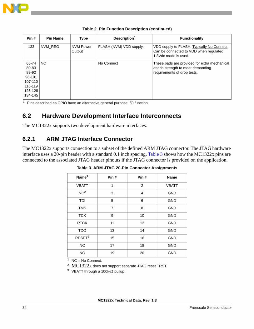
6.2 Hardware Development Interface InterconnectsThe MC1322x supports two development hardware interfaces.
6.2.1 ARM JTAG Interface ConnectorThe MC1322x supports connection to a subset of the defined ARM JTAG connector. The JTAG hardware interface uses a 20-pin header with a standard 0.1 inch spacing. Table 3 shows how the MC1322x pins are connected to the associated JTAG header pinouts if the JTAG connector is provided on the application.
133 NVM_REG NVM Power Output
FLASH (NVM) VDD supply. VDD supply to FLASH. Typically No Connect. Can be connected to VDD when regulated 1.8Vdc mode is used.
65-7480-8389-92
98-101107-110116-119125-128134-145
NC No Connect These pads are provided for extra mechanical attach strength to meet demanding requirements of drop tests.
1 Pins described as GPIO have an alternative general purpose I/O function.
Table 3. ARM JTAG 20-Pin Connector Assignments
Name1
1 NC = No Connect.
Pin # Pin # Name
VBATT 1 2 VBATT
NC2
2 MC1322x does not support separate JTAG reset TRST.
3 4 GND
TDI 5 6 GND
TMS 7 8 GND
TCK 9 10 GND
RTCK 11 12 GND
TDO 13 14 GND
RESET3
3 VBATT through a 100k-Ω pullup.
15 16 GND
NC 17 18 GND
NC 19 20 GND
Table 2. Pin Function Description (continued)
Pin # Pin Name Type Description1 Functionality
MC1322x Technical Data, Rev. 1.3
Freescale Semiconductor 35
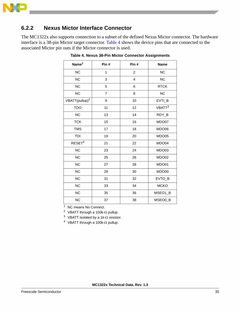
6.2.2 Nexus Mictor Interface ConnectorThe MC1322x also supports connection to a subset of the defined Nexus Mictor connector. The hardware interface is a 38-pin Mictor target connector. Table 4 shows the device pins that are connected to the associated Mictor pin outs if the Mictor connector is used.
Table 4. Nexus 38-Pin Mictor Connector Assignments
Name1
1 NC means No Connect.
Pin # Pin # Name
NC 1 2 NC
NC 3 4 NC
NC 5 6 RTCK
NC 7 8 NC
VBATT(pullup)2
2 VBATT through a 100k-Ω pullup.
9 10 EVTI_B
TDO 11 12 VBATT3
3 VBATT isolated by a 1k-Ω resistor.
NC 13 14 RDY_B
TCK 15 16 MDO07
TMS 17 18 MDO06
TDI 19 20 MDO05
RESET4
4 VBATT through a 100k-Ω pullup.
21 22 MDO04
NC 23 24 MDO03
NC 25 26 MDO02
NC 27 28 MDO01
NC 29 30 MDO00
NC 31 32 EVTO_B
NC 33 34 MCKO
NC 35 36 MSEO1_B
NC 37 38 MSEO0_B

MC1322x Technical Data, Rev. 1.3
36 Freescale Semiconductor
7 System Electrical SpecificationThis section details maximum ratings for the 99-pin LGA package and recommended operating conditions, DC characteristics, and AC characteristics.
7.1 LGA Package Maximum RatingsAbsolute maximum ratings are stress ratings only, and functional operation at the maximum rating is not guaranteed. Stress beyond the limits specified in Table 5 may affect device reliability or cause permanent damage to the device. For functional operating conditions, refer to the remaining tables in this section.
This device contains circuitry protecting against damage due to high static voltage or electrical fields; however, it is advised that normal precautions be taken to avoid application of any voltages higher than maximum-rated voltages to this high-impedance circuit. Reliability of operation is enhanced if unused inputs are tied to an appropriate logic voltage level (for instance, either VSS or VBATT) or the programmable pull-up resistor associated with the pin is enabled.
Table 5 shows the maximum ratings for the 99-Pin LGA package.Table 5. LGA Package Maximum Ratings
Rating Symbol Value Unit
Maximum Junction Temperature TJ 125 °C
Storage Temperature Range Tstg -55 to 125 °C
Moisture Sensitivity Level MSL3-260
Reflow Soldering Temperature (for reflow soldering profile and other LGA module reference information, see Freescale Application Note, AN3311)
260 °C
Power Supply Voltage VBATT, VDDINT -0.3 to 3.7 Vdc
Digital Input Voltage Vin -0.3 to (VDDINT + 0.2) Vdc
RF Input Power Pmax 10 dBm
Note: Maximum Ratings are those values beyond which damage to the device may occur. Functional operation should be restricted to the limits in the Electrical Characteristics or Recommended Operating Conditions tables.
Note: Meets Human Body Model (HBM) = 2 kV. RF input/output pins have no ESD protection.
MC1322x Technical Data, Rev. 1.3
Freescale Semiconductor 37
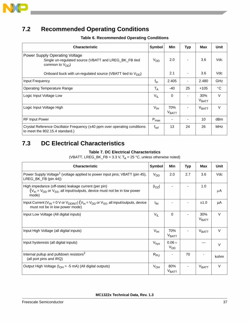
7.2 Recommended Operating Conditions
7.3 DC Electrical Characteristics
Table 6. Recommended Operating Conditions
Characteristic Symbol Min Typ Max Unit
Power Supply Operating VoltageSingle un-regulated source (VBATT and LREG_BK_FB tied common to VDD)
Onboard buck with un-regulated source (VBATT tied to VDD)
VDD 2.0
2.1
-
-
3.6
3.6
Vdc
Vdc
Input Frequency fin 2.405 - 2.480 GHz
Operating Temperature Range TA -40 25 +105 °C
Logic Input Voltage Low VIL 0 - 30% VBATT
V
Logic Input Voltage High VIH 70% VBATT
- VBATT V
RF Input Power Pmax - - 10 dBm
Crystal Reference Oscillator Frequency (±40 ppm over operating conditions to meet the 802.15.4 standard.)
fref 13 24 26 MHz
Table 7. DC Electrical Characteristics (VBATT, LREG_BK_FB = 3.3 V, TA = 25 °C, unless otherwise noted)
Characteristic Symbol Min Typ Max Unit
Power Supply Voltage1 (voltage applied to power input pins; VBATT (pin 45), LREG_BK_FB (pin 44))
VDD 2.0 2.7 3.6 Vdc
High impedance (off-state) leakage current (per pin)(VIn = VDD or VSS, all input/outputs, device must not be in low power mode)
|IOZ| - - 1.0μA
Input Current (VIN = 0 V or VDDINT) (VIn = VDD or VSS, all input/outputs, device must not be in low power mode)
IIN - - ±1.0 µA
Input Low Voltage (All digital inputs) VIL 0 - 30% VBATT
V
Input High Voltage (all digital inputs) VIH 70% VBATT
- VBATT V
Input hysteresis (all digital inputs) Vhys 0.06 × VDD
— V
Internal pullup and pulldown resistors2
(all port pins and IRQ) RPU - 70 - kohm
Output High Voltage (IOH = -5 mA) (All digital outputs) VOH 80% VBATT
- VBATT V

MC1322x Technical Data, Rev. 1.3
38 Freescale Semiconductor
7.4 Supply Current Characteristics
Output Low Voltage (IOL = 5 mA) (All digital outputs) VOL 0 - 20% VBATT
V
Maximum current in/out per IO pin — TBD mA
Maximum total IOL for all IO pins IOLT — TBD mA
Input capacitance (all non-supply pins) CIn — 3 — pF1 Maximum usable range of the reference voltage supply pin. This range may be modified because of the power supply
configuration used in an application. See Table 6, “Power Supply Voltage”.2 Measurement condition for pull resistors: VIN = VSS for pullup and VIN = VDD for pulldown.
Table 8. Supply Current Characteristics (VBATT, LREG_BK_FB = 3.3 V, TA = 25 °C, unless otherwise noted)
Characteristics Symbol Min Typ Max Unit
Off current - Device is in reset condition (held in reset) and all GPIO at ground. 0.4 0.6 μA
Hibernate current -RAM retained (8k, 32k, 64k, or 96k)2KHz onboard oscillator or 32 kHz crystal oscillatorCPU off (stop mode)wake-up from RTI timer, or external requestRadio offADCs not available
8 Kbyte RAM retention32 Kbyte RAM retention64 Kbyte RAM retention96 Kbyte RAM retention
0.92.33.75.1
2.24.9--
μAμAμAμA
Doze current -RAM retained (8k, 32k, 64k, or 96k)Onboard 24 MHz oscillator on (high frequency accuracy)CPU off (stop mode)Radio offADCs available, but inactive
8 Kbyte RAM retention32 Kbyte RAM retention64 Kbyte RAM retention96 Kbyte RAM retention
55575860
70---
μAμAμAμA
Idle current -All RAM activeReference oscillator on (24 MHz) at 1.2 VDCCPU on at 1 MHzReference clock available to all peripheralsRadio offADCs available, but inactive 0.85 .95 mA
Table 7. DC Electrical Characteristics (continued) (VBATT, LREG_BK_FB = 3.3 V, TA = 25 °C, unless otherwise noted)
Characteristic Symbol Min Typ Max Unit

MC1322x Technical Data, Rev. 1.3
Freescale Semiconductor 39
7.5 RF AC Electrical Characteristics
Run current -All RAM activeReference oscillator on (24 MHz) at 1.2 VDCCPU on at reference frequencyRadio offReference clock available to all peripheralsADCs available, but inactive 3.3 7.3 mA
Receive current -All RAM activeReference oscillator on (24MHZ) at 1.2 VDCRadio RX on (receiving data)Reference clock available to all peripheralsADC_1 available, but inactive
CPU on at 2 MHz (DCD)CPU on at 2 MHz (NCD)
2224
25-
mA
Transmit current -All RAM activeReference oscillator on (24MHZ) at 1.2 VDCRadio TX on (sending data @ 0 dBm)Reference clock available to all peripheralsADCs available, but inactive
CPU clock at 2 MHz 29 31 mA
Table 9. Receiver AC Electrical Characteristics for 802.15.4 Modulation Mode(VBATT, LREG_BK_FB = 3.3 V, TA = 25 °C, fref = 24 MHz, unless otherwise noted.)
Characteristic Symbol Min Typ Max Unit
Sensitivity for 1% Packet Error Rate (PER)1 (+25 °C, @ package interface; die sensitivity is ~1dB greater)
Non-coherent Differential Chip Detection (DCD)Non-coherent Detection (NCD)
1 The digital modem contains a block designated as the RX Modem. The Rx Modem can operate in: 1) Non-coherent Differential Chip Detection (DCD) mode which has 3-4dBm less sensitivity but requires 3-4mA less receiver current, and 2) Non-coherent Detection (NCD) mode which has 3-4dBm greater sensitivity but requires 3-4mA greater receiver current.
--
-96-100
-91-
dBm
Saturation (maximum input level) SENSmax - 10 - dBm
Channel Rejection for 1% PER (desired signal -82 dBm)+5 MHz (adjacent channel)-5 MHz (adjacent channel)+10 MHz (alternate channel)-10 MHz (alternate channel)>= 15 MHz
-----
3838575765
3535505060
dB
Frequency Error Tolerance2
2 Minimum set by IEEE 802.15.4 Standard
200 300 - kHz
Symbol Rate Error Tolerance2 80 120 - ppm
Table 8. Supply Current Characteristics (continued) (VBATT, LREG_BK_FB = 3.3 V, TA = 25 °C, unless otherwise noted)
Characteristics Symbol Min Typ Max Unit
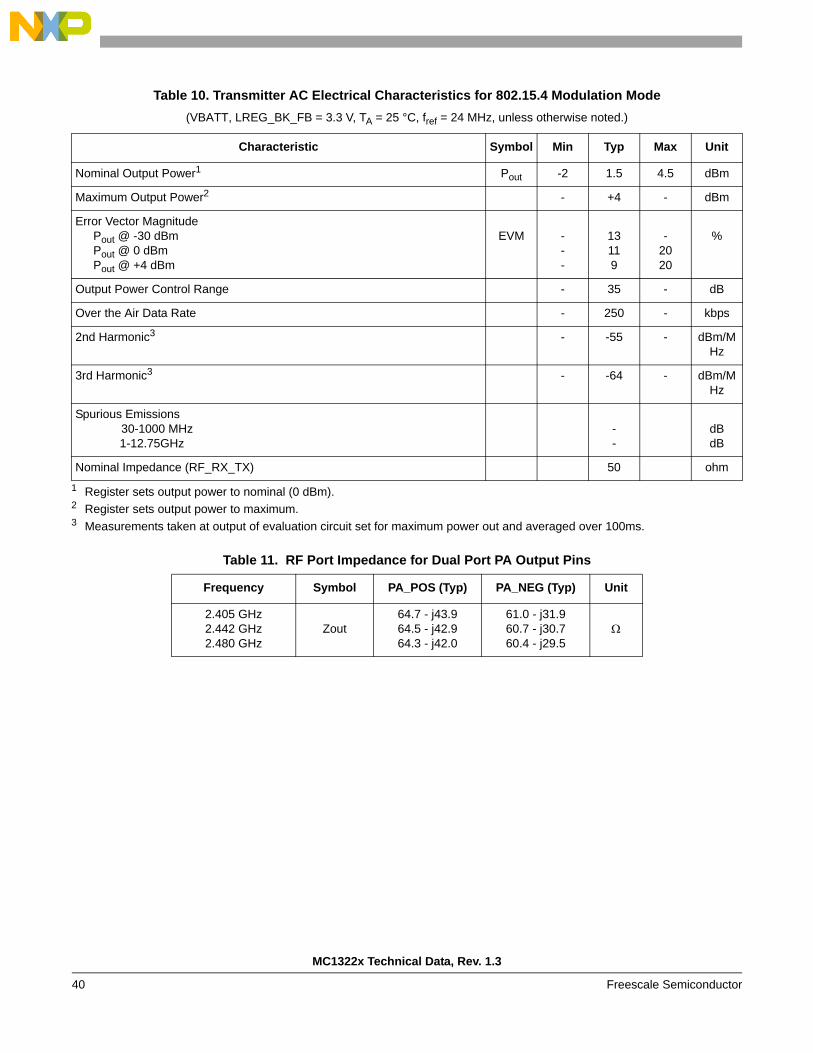
MC1322x Technical Data, Rev. 1.3
40 Freescale Semiconductor
Table 11. RF Port Impedance for Dual Port PA Output Pins
Table 10. Transmitter AC Electrical Characteristics for 802.15.4 Modulation Mode(VBATT, LREG_BK_FB = 3.3 V, TA = 25 °C, fref = 24 MHz, unless otherwise noted.)
Characteristic Symbol Min Typ Max Unit
Nominal Output Power1
1 Register sets output power to nominal (0 dBm).
Pout -2 1.5 4.5 dBm
Maximum Output Power2
2 Register sets output power to maximum.
- +4 - dBm
Error Vector MagnitudePout @ -30 dBmPout @ 0 dBmPout @ +4 dBm
EVM ---
13119
-2020
%
Output Power Control Range - 35 - dB
Over the Air Data Rate - 250 - kbps
2nd Harmonic3
3 Measurements taken at output of evaluation circuit set for maximum power out and averaged over 100ms.
- -55 - dBm/MHz
3rd Harmonic3 - -64 - dBm/MHz
Spurious Emissions30-1000 MHz1-12.75GHz
--
dBdB
Nominal Impedance (RF_RX_TX) 50 ohm
Frequency Symbol PA_POS (Typ) PA_NEG (Typ) Unit
2.405 GHz2.442 GHz2.480 GHz
Zout64.7 - j43.964.5 - j42.964.3 - j42.0
61.0 - j31.960.7 - j30.760.4 - j29.5
Ω

MC1322x Technical Data, Rev. 1.3
Freescale Semiconductor 41
7.6 Crystal Reference Clock Oscillator CharacteristicsThe reference oscillator model including external crystal in shown in Figure 10. The IEEE 802.15.4 Standard requires a frequency tolerance less than or equal to +/- 40 ppm as shown in the oscillator specification Table 12. With a suitable crystal (refer to Table 13 and Freescale Application Note AN3251), the device frequency tolerance can typically trimmed to be held to +/- 30 ppm over all conditions.
Figure 10. Reference Oscillator Model
Table 12. Reference Oscillator Specifications
Characteristic Symbol Min Typ Max Unit
Frequency 13 24 26 MHz
Oscillator frequency tolerance over temperature range. +/- 30 +/- 40 ppm
External load capacitance CLext None required (onboard) pF
Internal Osc startup time (13 MHz - 26 MHz)1
1 This is part of device wake-up time.
0.8 1.2 ms
Y1
CRYSTAL
2pF
Cstray
REFERENCEOSCILLATOR
1pF4pF8pF 2pF 1pF4pF8pF
OSC_IN OSC_OUT
0-5pF with steps of 160 fF.
0-5pFwith steps of 160 fF.
Cstray
Course Tune[3:0]
Fine Tune[4:0]
1 MEG (nom)
MC13224V
4pF
Course Tune[4]
4pF
Course Tune[4]
Course Tune[3:0]
Fine Tune[4:0]
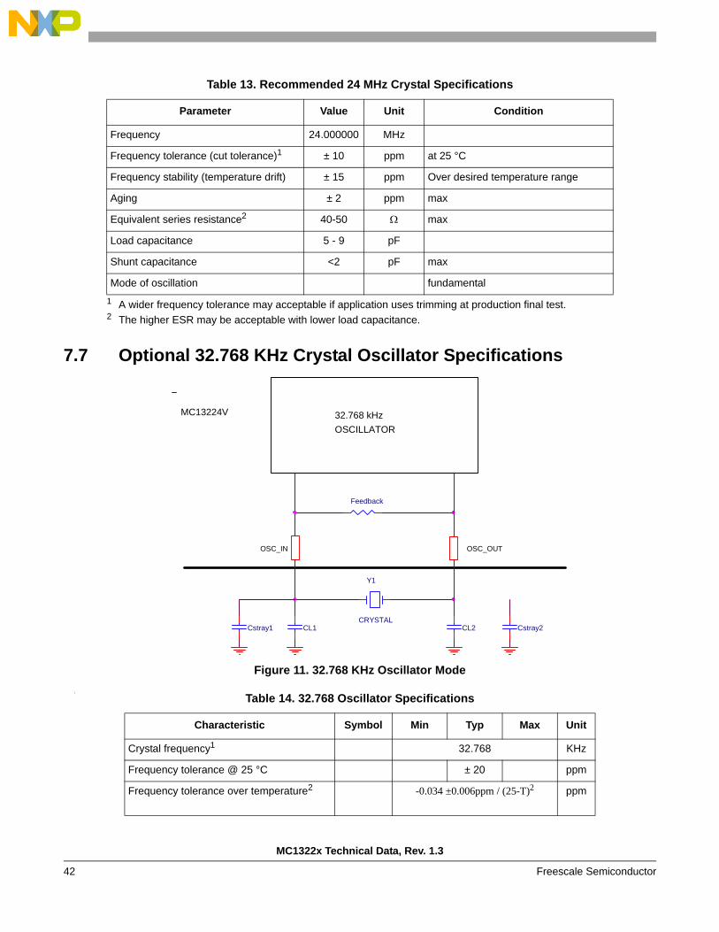
MC1322x Technical Data, Rev. 1.3
42 Freescale Semiconductor
7.7 Optional 32.768 KHz Crystal Oscillator Specifications
Figure 11. 32.768 KHz Oscillator Model
Table 13. Recommended 24 MHz Crystal Specifications
Parameter Value Unit Condition
Frequency 24.000000 MHz
Frequency tolerance (cut tolerance)1
1 A wider frequency tolerance may acceptable if application uses trimming at production final test.
± 10 ppm at 25 °C
Frequency stability (temperature drift) ± 15 ppm Over desired temperature range
Aging ± 2 ppm max
Equivalent series resistance2
2 The higher ESR may be acceptable with lower load capacitance.
40-50 Ω max
Load capacitance 5 - 9 pF
Shunt capacitance <2 pF max
Mode of oscillation fundamental
Table 14. 32.768 Oscillator Specifications
Characteristic Symbol Min Typ Max Unit
Crystal frequency1 32.768 KHz
Frequency tolerance @ 25 °C ± 20 ppm
Frequency tolerance over temperature2 -0.034 ±0.006ppm / (25-T)2 ppm
Y1
CRYSTALCL1
32.768 kHzOSCILLATOR
OSC_IN OSC_OUT
CL2
Feedback
MC13224V
Cstray1 Cstray2
MC1322x Technical Data, Rev. 1.3
Freescale Semiconductor 43
7.8 Internal Low Speed Reference Oscillator Specifications
7.9 Control Timing and CPU Bus Specifications
7.9.1 Timer Module Input CharacteristicsFour-bit synchronizer circuits determine the shortest input pulses that can be recognized or the fastest clock that can be used as the optional external source to the timer counter. These synchronizers operate from the peripheral clock rate. Table 17 shows timer input timing values.
Load capacitance 11 12.5 13 pF
Equivalent series resistance (ESR) 60 kΩ
Shunt capacitance 1.35 pF
Tolerated drive level 1 μW1 Recommended crystal Abracom Corporation crystal part number ABS25-32.768-12.5-B2 Example; Stability at -20×C is: -0.034 x (25-[-20])2= -68.8ppm.
Table 15. Internal 2 KHz Oscillator Specifications
Characteristic Symbol Min Typ Max Unit
Default Frequency @ 25 °C 2.5 1.7 3.5 KHz
Oscillator frequency variation over full temperature range - +/- 13 - %
Calibration time (in terms of 2KHz osc clocks) - - 216-1 osc clks
Table 16. MCU Control Timing
(VBATT, LREG_BK_FB = 3.3 V, TA = 25 °C, fref = 24 MHz, unless otherwise noted.)
Parameter Symbol Min Typical Max Unit
CPU Bus frequency (tcyc = 1/fBus) fBus fref/64 1
1 Normal operation uses a 24 MHz reference. The MC1322x allows up to a 26 MHz max reference oscillator.
— fref 1 MHz
CPU Bus frequency with active TX or RX 2 MHz
Real-time interrupt internal oscillator frequency 2 KHz
External reset pulse width2
2 This is the shortest pulse that is guaranteed to be recognized as a reset pin request. There always must be 3 clocks of the operating oscillator; this can vary from the low power oscillators to the reference oscillator.
- 4 — osc clks
External minimum interrupt pulse width (KBI[7:4]) - 4 — osc clks
Table 14. 32.768 Oscillator Specifications (continued)
Characteristic Symbol Min Typ Max Unit
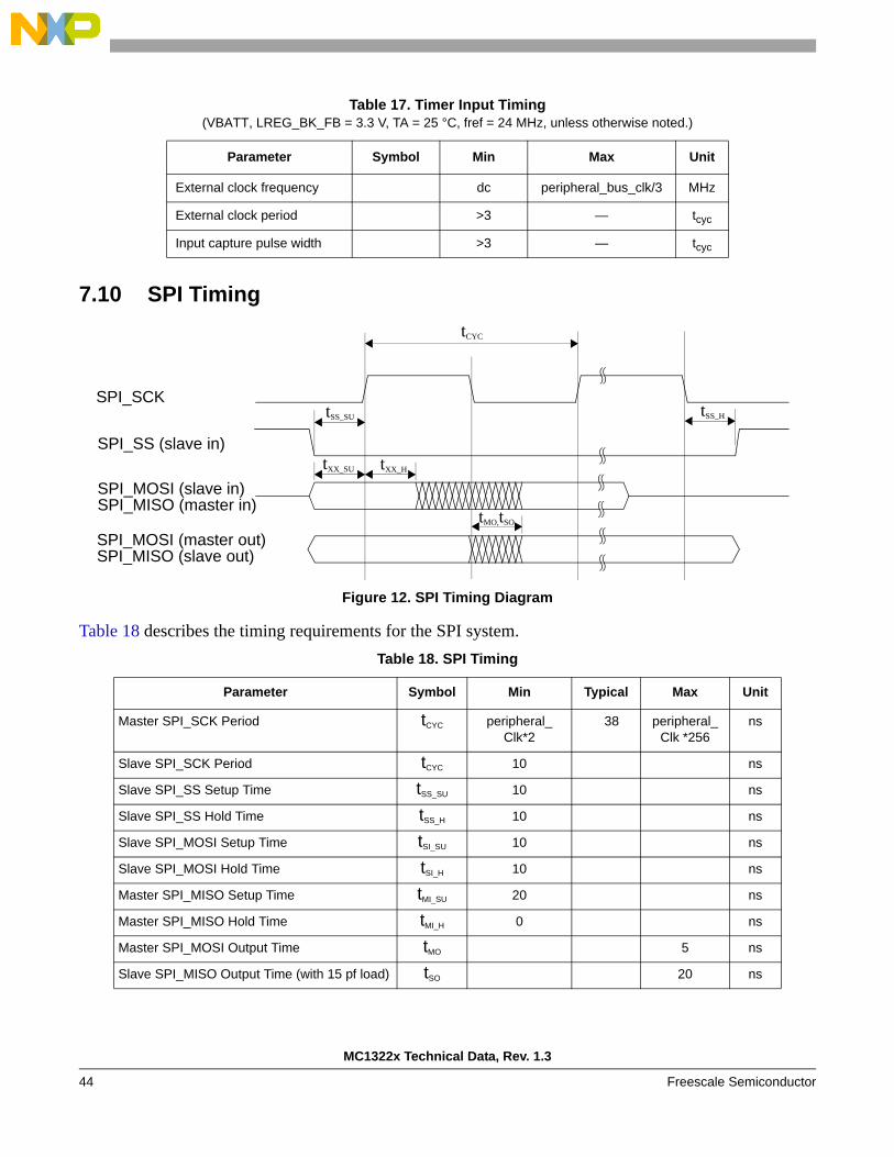
MC1322x Technical Data, Rev. 1.3
44 Freescale Semiconductor
7.10 SPI Timing
Figure 12. SPI Timing Diagram
Table 18 describes the timing requirements for the SPI system.
Table 17. Timer Input Timing(VBATT, LREG_BK_FB = 3.3 V, TA = 25 °C, fref = 24 MHz, unless otherwise noted.)
Parameter Symbol Min Max Unit
External clock frequency dc peripheral_bus_clk/3 MHz
External clock period >3 — tcyc
Input capture pulse width >3 — tcyc
Table 18. SPI Timing
Parameter Symbol Min Typical Max Unit
Master SPI_SCK Period tCYC peripheral_Clk*2
38 peripheral_Clk *256
ns
Slave SPI_SCK Period tCYC 10 ns
Slave SPI_SS Setup Time tSS_SU 10 ns
Slave SPI_SS Hold Time tSS_H 10 ns
Slave SPI_MOSI Setup Time tSI_SU 10 ns
Slave SPI_MOSI Hold Time tSI_H 10 ns
Master SPI_MISO Setup Time tMI_SU 20 ns
Master SPI_MISO Hold Time tMI_H 0 ns
Master SPI_MOSI Output Time tMO 5 ns
Slave SPI_MISO Output Time (with 15 pf load) tSO 20 ns
SPI_SCK
SPI_MOSI (slave in)
SPI_SS (slave in)
SPI_MISO (master in)
tXX_SU tXX_H
tCYC
tSS_SU tSS_H
tMO,tSO
SPI_MOSI (master out)SPI_MISO (slave out)
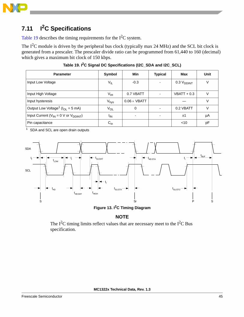
MC1322x Technical Data, Rev. 1.3
Freescale Semiconductor 45
7.11 I2C SpecificationsTable 19 describes the timing requirements for the I2C system.
The I2C module is driven by the peripheral bus clock (typically max 24 MHz) and the SCL bit clock is generated from a prescaler. The prescaler divide ratio can be programmed from 61,440 to 160 (decimal) which gives a maximum bit clock of 150 kbps.
Figure 13. I2C Timing Diagram
NOTEThe I2C timing limits reflect values that are necessary meet to the I2C Bus specification.
Table 19. I2C Signal DC Specifications (I2C_SDA and I2C_SCL)
Parameter Symbol Min Typical Max Unit
Input Low Voltage VIL -0.3 - 0.3 VDDINT V
Input High Voltage VIH 0.7 VBATT - VBATT + 0.3 V
Input hysteresis Vhys 0.06 × VBATT — V
Output Low Voltage1 (IOL = 5 mA)
1 SDA and SCL are open drain outputs
VOL 0 - 0.2 VBATT V
Input Current (VIN = 0 V or VDDINT) IIN - - ±1 µA
Pin capacitance Cin <10 pF
SDA
SCL
tf
tHD
tLOWtr
tHD;DAT
tSU;DAT
tHIGH
tf
S Sr
tSU;STA
tHD:STA
P
trtBUF
S
tSU;STO

MC1322x Technical Data, Rev. 1.3
46 Freescale Semiconductor
Table 20. I2C Signal AC Specifications1
1 All values referred to VIHmin and VILmax levels
Parameter Symbol Standard-Mode Fast-Mode Unit
Min Max Min Max
SCL clock frequency (when source) fSCL 0 100 0 150 kHz
Hold time (repeated) START condition.After this period, the first clock pulse is generated
tHD;STA 4.0 - 0.6 - μs
LOW period of the SCL clock tLOW 4.7 - 1.3 - μs
HIGH period of the SCL clock tHIGH 4.0 - 0.6 - μs
Set-up time for a repeated START condition tSU;STA 4.7 - 0.6 - μs
Data hold time tSHD;DAT 02
2 A device must internally provide a hold time of at least 300 ns for the SDA signal (referred to the VIHmin of the SCLsignal) to bridge the undefined region of the falling edge of SCL.
3.453
3 The maximum tHD;DAT has only to be met if the device does not stretch the LOW period (tLOW) of the SCL signal.
02 0.93 μs
Data setup time tSU:DAT 250 - 1004
4 A Fast-mode I2C-bus device can be used in a Standard-mode I2C-bus system, but the requirement tSU;DAT >= 250 nsmust then be met. This will automatically be the case if the device does not stretch the LOW period of the SCL signal.If such a device does stretch the LOW period of the SCL signal, it must output the next data bit to the SDA line tr max+ tSU;DAT = 1000 + 250 = 1250 ns (according to the Standard-mode I2C-bus specification) before the SCL line isreleased.
- ns
Rise time for both SDA and SCL signals tr - 1000 20 + 0.1Cb
5
5 Cb = total capacitance of one bus line in pF. If mixed with Hs-mode devices, the faster fall-times are allowed.
300 ns
Fall time for both SDA and SCL signals tf - 300 20 + 0.1Cb
5300 ns
Bus free time between a STOP and START condition tBUF 4.7 - 1.3 - μs
Capacitive load for each bus line Cb - 400 - 400 pF
MC1322x Technical Data, Rev. 1.3
Freescale Semiconductor 47
7.12 FLASH Specifications
7.13 ADC Characteristics
Table 21. FLASH Characteristics(TA = 25 °C, fref = 24 MHz, unless otherwise noted.)
Characteristic Symbol Min Typical Max Unit
Supply voltage for program/erase/read (with directly regulated supply) Vprog/erase 1.70 1.90 V
SPI clock frequency fFCLK 13 MHz
Read current (13 MHz) 9 15 mA
Program and erase current 10 15 mA
Standby current 2 10 μA
Sector erase duration 75 ms
Block erase duration 75 ms
Chip erase duration 150 ms
Byte program duration 60 μs
Program/erase endurance 100,000 cycles
Data retention tD_ret 100 — years
Table 22. ADC Electrical Characteristics (Operating)(VBATT, LREG_BK_FB = 3.3 V, TA = 25 °C, fref = 24 MHz, unless otherwise noted.)
Characteristic Condition Symbol Min Typical Max Unit
ADC supply current (per ADC)Enabled — 2.9 6 mA
Disabled — 5 - μA
Reference potential, low VREFL VSS — VREFH V
Reference potential, high VREFH VREFL — VBATT V
Analog input voltage1
1 Maximum electrical operating range, not valid conversion range.
VINDC VSS – 0.2 — VDD +0.2 V
“Battery” input channel reference voltage 1.2 V

MC1322x Technical Data, Rev. 1.3
48 Freescale Semiconductor
8 Developer EnvironmentThe MC1322x family is supported by a full set of hardware/software evaluation and development tools.
8.1 Hardware Development InterfacesThe ARM debug environment supports both a JTAG debug interface and an extended capability Nexus interface.
8.1.1 JTAG Hardware Debug PortThe JTAG port is the simpler and more common debug port for the ARM core. A standard 20-pin connector as described in Section 6.2.1, “ARM JTAG Interface Connector””, is connected to the TDI, TMS, TCK, TDO, and RTCK signals of the MC1322x. Through the JTAG serial interface, standard debug and development activities such as accessing memory and registers, control of the CPU, download of FLASH memory, and software debug can be accomplished.
8.1.2 A7S Nexus3 (NEX) ARM7 Core Development InterfaceThe development and debug environment of the ARM7TDMI-S core is based on the A7S Nexus3 interface (compliant with a Class 3 device of the IEEE-ISTO 5001 standard for real-time embedded system design). This interface allows expansion of the development features of the JTAG port (through the addition of auxiliary signals, see Section 6.2.2, “Nexus Mictor Interface Connector”). Development features include:
• Program Trace via Branch Trace Messaging (BTM). Branch trace messaging displays program flow discontinuities (direct and indirect branches, exceptions, etc.), allowing the development tool to interpolate what transpires between the discontinuities. Thus static code may be traced.
Table 23. ADC Timing/Performance Characteristics
Characteristic Symbol Condition Min Typ Max Unit
Resolution - 12 Bits
Effective Resolution 8 Bits
Number of input channels 8
ADC conversion clock frequency fADCCLK - - 300 KHz
Conversion cycles (continuous convert) CCP 6 ADCCLK cycles
Conversion time Tconv 20 — - μs
Input Leakage Current — — - nA
Analog Input Voltage1
1 Analog input must be between VREFL + 0.2 and VREFH - 0.2 for valid conversion.
VAIN VDD VREFL VREFH V

MC1322x Technical Data, Rev. 1.3
Freescale Semiconductor 49
• Data Trace via Data Write Messaging (DWM) and Data Read Messaging (DRM). This provides the capability for the development tool to trace reads and/or writes to (selected) internal memory resources.
• Ownership Trace via Ownership Trace Messaging (OTM). OTM facilitates ownership trace by providing visibility of which process ID or operating system task is activated. An Ownership Trace Message is transmitted when a new process/task is activated, allowing the development tool to trace ownership flow.
• Run-time access to the memory map via the JTAG port. This allows for enhanced download/upload capabilities
• Watchpoint Messaging (WPM) via the auxiliary pins• Watchpoint Trigger enable of Program and/or Data Trace Messaging• Auxiliary interface for higher data input/output• Registers for Program Trace, Ownership Trace, Watchpoint Trigger, and Read/Write Access• Programmable processor stall function to mitigate message queue overrun risk• All features controllable and configurable via the JTAG port
8.2 Software Development ToolsAn Integrated Development Environment (IDE) is available to facilitate the development of embedded applications targeting the MC1322x platform. Features of the IDE include:
• Project management tools and code editor• Highly optimizing ARM compiler supporting C and C++• Extensive JTAG and RDI debugger support• Run-time libraries including source code• Relocating ARM assembler• Linker and librarian tools• Debugger with ARM simulator, JTAG support and support for RTOS-aware debugging on
hardware• RTOS plug-ins available • Code templates for commonly used code constructs• Sample projects for evaluation boards• User and reference guides, both printed and in PDF format• Context-sensitive online help
The IDE is complemented by the BeeKit™ Wireless Connectivity Toolkit. BeeKit is a stand alone software application targeting Windows® operating systems. BeeKit provides a graphical user interface (GUI) in which users can create, modify, save, and update wireless networking solutions. With the solution explorer property list windows, users can set configuration parameters to control the setup and execution behavior of the wireless link within their application. The configuration parameters can be validated inside BeeKit to ensure all values provided are within acceptable ranges prior to generation of a workspace. All this functionality provides a mechanism for developers to configure and validate their network parameters

MC1322x Technical Data, Rev. 1.3
50 Freescale Semiconductor
without having to navigate through multiple source files to configure the same parameters. BeeKit supports Freescale’s Simple MAC (SMAC), IEEE 802.15.4-compliant MAC, and the Freescale BeeStack™.
8.3 Development HardwareSeveral different development modules and kits will be available to allow evaluation of ZigBee and IEEE 802.15.4 applications. The modules will provide capabilities for Coordinator, Router, and End Device nodes. Reference designs will be available for RF design and low power applications including 2-layer and 4-layer PCBs.

MC1322x Technical Data, Rev. 1.3
Freescale Semiconductor 51
9 Mechanical Diagrams(Case 1901-01, non-JEDEC)
Figure 14. Mechanical Diagram (1 of 2)

MC1322x Technical Data, Rev. 1.3
52 Freescale Semiconductor
Figure 15. Mechanical Diagram Bottom View (2 of 2)

NOTES
MC1322x Technical Data, Rev. 1.3
Freescale Semiconductor 53
Document Number: MC1322xRev. 1.310/2010
How to Reach Us:
Home Page:www.freescale.com
E-mail:[email protected]
USA/Europe or Locations Not Listed:Freescale SemiconductorTechnical Information Center, CH3701300 N. Alma School RoadChandler, Arizona 85224+1-800-521-6274 or [email protected]
Europe, Middle East, and Africa:Freescale Halbleiter Deutschland GmbHTechnical Information CenterSchatzbogen 781829 Muenchen, Germany+44 1296 380 456 (English)+46 8 52200080 (English)+49 89 92103 559 (German)+33 1 69 35 48 48 (French)[email protected]
Japan:Freescale Semiconductor Japan Ltd.HeadquartersARCO Tower 15F1-8-1, Shimo-Meguro, Meguro-ku,Tokyo 153-0064, Japan0120 191014 or +81 3 5437 [email protected]
Asia/Pacific:Freescale Semiconductor Hong Kong Ltd.Technical Information Center2 Dai King StreetTai Po Industrial EstateTai Po, N.T., Hong Kong+800 2666 [email protected]
For Literature Requests Only:Freescale Semiconductor Literature Distribution CenterP.O. Box 5405Denver, Colorado 802171-800-521-6274 or 303-675-2140Fax: [email protected]
Information in this document is provided solely to enable system and software implementers to use Freescale Semiconductor products. There are no express or implied copyright licenses granted hereunder to design or fabricate any integrated circuits or integrated circuits based on the information in this document.Freescale Semiconductor reserves the right to make changes without further notice to any products herein. Freescale Semiconductor makes no warranty, representation or guarantee regarding the suitability of its products for any particular purpose, nor does Freescale Semiconductor assume any liability arising out of the application or use of any product or circuit, and specifically disclaims any and all liability, including without limitation consequential or incidental damages. “Typical” parameters that may be provided in Freescale Semiconductor data sheets and/or specifications can and do vary in different applications and actual performance may vary over time. All operating parameters, including “Typicals”, must be validated for each customer application by customer’s technical experts. Freescale Semiconductor does not convey any license under its patent rights nor the rights of others. Freescale Semiconductor products are not designed, intended, or authorized for use as components in systems intended for surgical implant into the body, or other applications intended to support or sustain life, or for any other application in which the failure of the Freescale Semiconductor product could create a situation where personal injury or death may occur. Should Buyer purchase or use Freescale Semiconductor products for any such unintended or unauthorized application, Buyer shall indemnify and hold Freescale Semiconductor and its officers, employees, subsidiaries, affiliates, and distributors harmless against all claims, costs, damages, and expenses, and reasonable attorney fees arising out of, directly or indirectly, any claim of personal injury or death associated with such unintended or unauthorized use, even if such claim alleges that Freescale Semiconductor was negligent regarding the design or manufacture of the part.
Freescale and the Freescale logo are trademarks or registered trademarks of Freescale Semiconductor, Inc. in the U.S. and other countries. All other product or service names are the property of their respective owners. ARM is the registered trademark of ARM Limited. ARM7TDMI-S is the trademark of ARM Limited.© Freescale Semiconductor, Inc. 2006, 2007, 2008, 2009, 2010


