May 14, 2009 1ISVLSI 09
Algorithms for Estimating Number of Glitches and Dynamic Power in CMOS
Circuits with Delay Variations
Jins Davis AlexanderJins Davis AlexanderVishwani D. AgrawalVishwani D. Agrawal
Department of Electrical and Computer EngineeringAuburn University, Auburn, AL 36849
Presented at the IEEE Computer Society Annual Symposium on VLSI Tampa, Florida, May 13-15, 2009
May 14, 2009 2ISVLSI 09
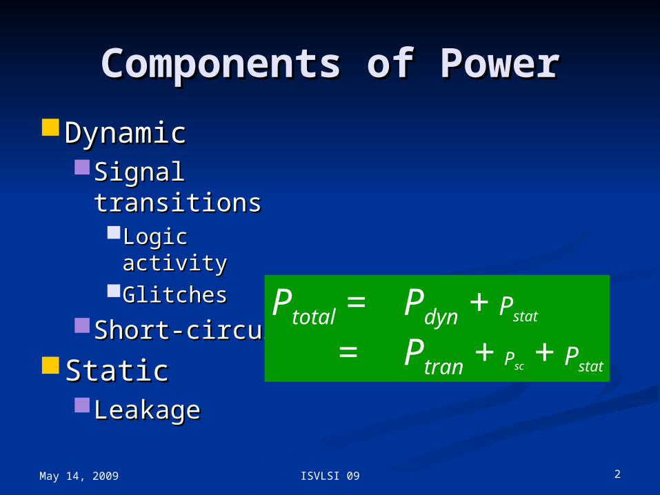
Components of PowerComponents of Power
DynamicDynamicSignal Signal
transitionstransitionsLogic activityLogic activityGlitchesGlitches
Short-circuitShort-circuitStaticStatic
LeakageLeakage
Ptotal = Pdyn + Pstat
= Ptran + Psc + Pstat
May 14, 2009 3ISVLSI 09
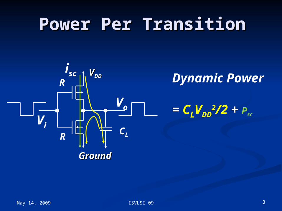
Power Per TransitionPower Per Transition
VVDDDD
GroundGround
CL
R
R
Dynamic Power
= CLVDD2/2 + Psc
Vi
Vo
isc

May 14, 2009 4ISVLSI 09
Number of TransitionsNumber of Transitions
May 14, 2009 5ISVLSI 09
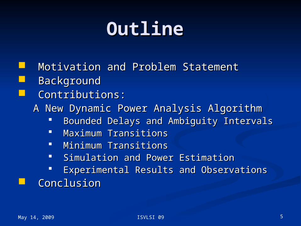
OutlineOutline
Motivation and Problem StatementMotivation and Problem Statement BackgroundBackground Contributions:Contributions:
A New Dynamic Power Analysis Algorithm A New Dynamic Power Analysis Algorithm Bounded Delays and Ambiguity IntervalsBounded Delays and Ambiguity Intervals Maximum TransitionsMaximum Transitions Minimum TransitionsMinimum Transitions Simulation and Power EstimationSimulation and Power Estimation Experimental Results and ObservationsExperimental Results and Observations
ConclusionConclusion
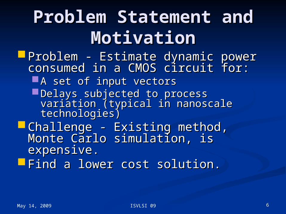
May 14, 2009 6ISVLSI 09
Problem Statement and Problem Statement and MotivationMotivation
Problem - Estimate dynamic power Problem - Estimate dynamic power consumed in a CMOS circuit for:consumed in a CMOS circuit for:A set of input vectorsA set of input vectorsDelays subjected to process variation Delays subjected to process variation
(typical in nanoscale technologies)(typical in nanoscale technologies) Challenge - Existing method, Monte Challenge - Existing method, Monte
Carlo simulation, is expensive.Carlo simulation, is expensive. Find a lower cost solution.Find a lower cost solution.
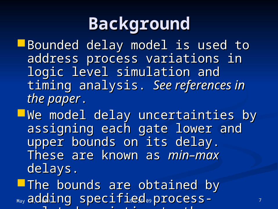
May 14, 2009 7ISVLSI 09
BackgroundBackgroundBounded delay model is used to Bounded delay model is used to
address process variations in logic address process variations in logic level simulation and timing analysis. level simulation and timing analysis. See references in the paperSee references in the paper..
We model delay uncertainties by We model delay uncertainties by assigning each gate lower and upper assigning each gate lower and upper bounds on its delay. These are bounds on its delay. These are known as known as min–max min–max delays.delays.
The bounds are obtained by adding The bounds are obtained by adding specified process-related variation to specified process-related variation to the nominal gate delay for the the nominal gate delay for the technology.technology.
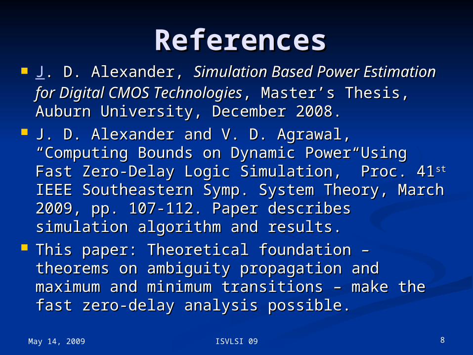
ReferencesReferences J. D. Alexander, . D. Alexander, Simulation Based Power Simulation Based Power
Estimation for Digital CMOS TechnologiesEstimation for Digital CMOS Technologies, , Master’s Thesis, Auburn University, December Master’s Thesis, Auburn University, December 2008.2008.
J. D. Alexander and V. D. Agrawal, “Computing J. D. Alexander and V. D. Agrawal, “Computing Bounds on Dynamic Power Using Fast Zero-Delay Bounds on Dynamic Power Using Fast Zero-Delay Logic Simulation,” Proc. 41Logic Simulation,” Proc. 41stst IEEE Southeastern IEEE Southeastern Symp. System Theory, March 2009, pp. 107-112. Symp. System Theory, March 2009, pp. 107-112. Paper describes simulation algorithm and results.Paper describes simulation algorithm and results.
This paper: Theoretical foundation – theorems on This paper: Theoretical foundation – theorems on ambiguity propagation and maximum and ambiguity propagation and maximum and minimum transitions – make the fast zero-delay minimum transitions – make the fast zero-delay analysis possible.analysis possible.
May 14, 2009 8ISVLSI 09

May 14, 2009 9ISVLSI 09
Ambiguity IntervalsAmbiguity Intervals
• EA is the earliest arrival time• LS is the latest stabilization time• IV is the initial signal value• FV is the final signal value
IV FV
LSEA
IV FV
EA LS
EAdv LSdv
EAsv=-∞ LSsv=∞
EAsv LSsv
EAdv=-∞ LSdv=∞

May 14, 2009 10ISVLSI 09
Propagating Ambiguity Propagating Ambiguity Intervals through GatesIntervals through Gates
The ambiguity interval (EA,LS) for a gate output is determined by:•Ambiguity intervals of input signals.•Pre-transition and Post-transition steady-state values.•Min-Max gate delays.
(mindel, maxdel)

May 14, 2009 11ISVLSI 09
Representative FormulaeRepresentative FormulaeTo evaluate the output of a gate, we To evaluate the output of a gate, we
analyze inputs analyze inputs ii::

May 14, 2009 12ISVLSI 09
Theorem 1: Propagating Theorem 1: Propagating Ambiguity IntervalsAmbiguity Intervals
Ambiguity interval at a gate output is:Ambiguity interval at a gate output is:
where the inertial delay of the gate is where the inertial delay of the gate is bounded as (bounded as (mindelmindel, , maxdelmaxdel). ).
May 14, 2009 13ISVLSI 09
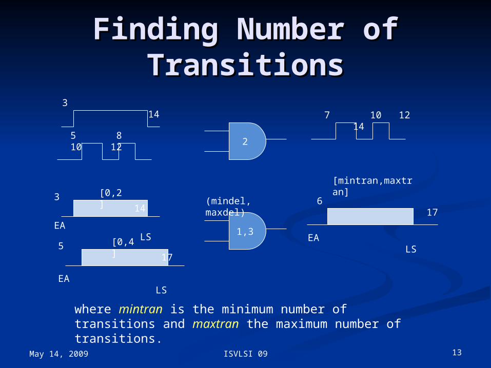
Finding Number of Finding Number of TransitionsTransitions
2
1,3
3 14
5 8 10 12
(mindel, maxdel)
7 10 12 14
5 17
EA LS
3 14
EA LS
[0,4]
[0,2] 6 17
EA LS
[mintran,maxtran]
where mintran is the minimum number of transitions and maxtran the maximum number of transitions.
May 14, 2009 14ISVLSI 09
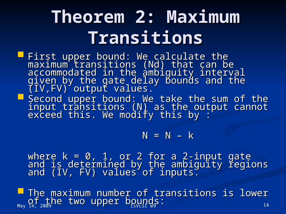
Theorem 2: Maximum Theorem 2: Maximum TransitionsTransitions
First upper bound: We calculate the maximum First upper bound: We calculate the maximum transitions (Nd) that can be accommodated in transitions (Nd) that can be accommodated in the ambiguity interval given by the gate delay the ambiguity interval given by the gate delay bounds and the (IV,FV) output values.bounds and the (IV,FV) output values.
Second upper bound: We take the sum of the Second upper bound: We take the sum of the input transitions (N) as the output cannot exceed input transitions (N) as the output cannot exceed this. We modify this by :this. We modify this by :
N = N – k N = N – k
where k = 0, 1, or 2 for a 2-input gate and is where k = 0, 1, or 2 for a 2-input gate and is determined by the ambiguity regions and (IV, determined by the ambiguity regions and (IV, FV) values of inputs.FV) values of inputs.
The maximum number of transitions is lower of The maximum number of transitions is lower of the two upper bounds:the two upper bounds:
maxtran = maxtran = minmin (Nd, N) (Nd, N)

May 14, 2009 15ISVLSI 09
Examples of Examples of maxtran maxtran ((k k = 0)= 0)
Nd = ∞
N = 8
maxtran=min (Nd, N) = 8
Nd = 6
N = 8
maxtran=min (Nd, N) = 6

May 14, 2009 16ISVLSI 09
Example: Example: maxtranmaxtran With With Non-Zero Non-Zero kk
EAsv = - ∞
EAdv
LSdv = ∞
LSsv
EAsv = - ∞ LSdv = ∞EAdv LSsv
EA LS [n1 = 6]
[n2 = 4]
[n1 + n2 – k = 8 ] ,
where k = 2
[ 6 ]
[ 4 ]
[ 6 + 4 – 2 = 8 ]

May 14, 2009 17ISVLSI 09
Theorem 3: Minimum Theorem 3: Minimum TransitionsTransitions
First lower bound First lower bound (Ns)(Ns): Based on steady state : Based on steady state values, i.e., 0values, i.e., 00, 10, 11 as no transition and 01 as no transition and 01, 1, 110 as a single transition. 0 as a single transition.
Second lower bound Second lower bound (Ndet)(Ndet): The minimum : The minimum number of transitions that can occur in the number of transitions that can occur in the output ambiguity region is the number of output ambiguity region is the number of deterministic signal changes that occur within deterministic signal changes that occur within the ambiguity region and such that signal the ambiguity region and such that signal changes are spaced at time intervals greater changes are spaced at time intervals greater than or equal to the inertial delay of the gate.than or equal to the inertial delay of the gate.
The minimum number of transitions is the higher The minimum number of transitions is the higher of the two lower bounds:of the two lower bounds:
mintranmintran = = max max (Ns, Ndet)(Ns, Ndet)
May 14, 2009 18ISVLSI 09
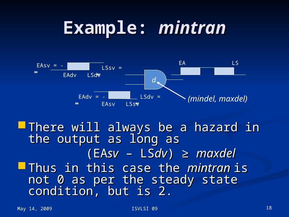
Example: Example: mintranmintran
There will always be a hazard in the There will always be a hazard in the output as long asoutput as long as
(EA(EAsvsv – LS – LSdvdv) ) ≥≥ maxdelmaxdel Thus in this case the Thus in this case the mintran mintran is not 0 is not 0
as per the steady state condition, but is as per the steady state condition, but is 2.2.
d
EAsv = - ∞
EAdv LSsv = ∞
LSdv
EAdv = - ∞ LSdv = ∞EAsv LSsv
EA LS
(mindel, maxdel)
May 14, 2009 19ISVLSI 09
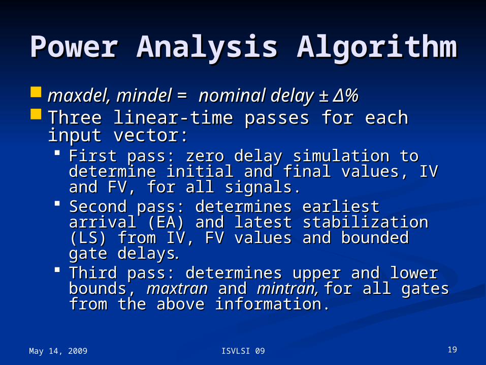
Power Analysis Power Analysis AlgorithmAlgorithm
maxdel, mindel maxdel, mindel = = nominal delay ± Δ%nominal delay ± Δ% Three linear-time passes for each input Three linear-time passes for each input
vector:vector: First pass: zero delay simulation to determine First pass: zero delay simulation to determine
initial and final values, IV and FV, for all initial and final values, IV and FV, for all signals.signals.
Second pass: determines earliest arrival (EA) Second pass: determines earliest arrival (EA) and latest stabilization (LS) from IV, FV values and latest stabilization (LS) from IV, FV values and bounded gate delaysand bounded gate delays..
Third pass: determines upper and lower Third pass: determines upper and lower bounds, bounds, maxtranmaxtran and and mintran, mintran, for all gates for all gates from the above information.from the above information.

May 14, 2009 20ISVLSI 09
Simulation SetupSimulation Setup
Standard gate delay 100 ps.Standard gate delay 100 ps. Wire-load model used; gate proportional Wire-load model used; gate proportional
to fan–out.to fan–out. The power distribution determined for The power distribution determined for
1000 random vectors with a vector period 1000 random vectors with a vector period of 10000 ps.of 10000 ps.
For each vector pair, 1000 sample circuits For each vector pair, 1000 sample circuits were simulated. were simulated.
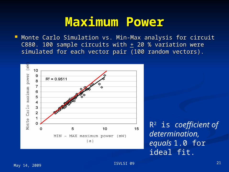
Maximum PowerMaximum Power Monte Carlo Simulation vs. Min-Max analysis for circuit Monte Carlo Simulation vs. Min-Max analysis for circuit
C880. 100 sample circuits with C880. 100 sample circuits with ++ 20 % variation were 20 % variation were simulated for each vector pair (100 random vectors).simulated for each vector pair (100 random vectors).
May 14, 2009 ISVLSI 09 21
R2 is coefficient of determination, equals 1.0 for ideal fit.

Minimum PowerMinimum Power
May 14, 2009 ISVLSI 09 22
R2 is coefficient of determination, equals 1.0 for ideal fit.

Average PowerAverage Power
R2 = 0.9527
0
1
2
3
4
5
6
7
8
9
10
0 2 4 6 8 10
MIN - MAX mean power (mW)
Mo
nte
Car
lo a
vera
ge
po
wer
(m
W)
R2 is coefficient of determination, equals 1.0 for ideal fit.
May 14, 2009 23ISVLSI 09
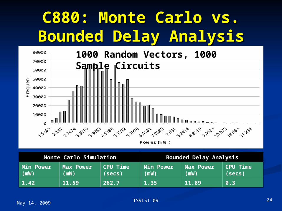
C880: Monte Carlo vs. C880: Monte Carlo vs. Bounded Delay AnalysisBounded Delay Analysis
May 14, 2009 ISVLSI 09 24
Monte Carlo Simulation Bounded Delay Analysis
Min Power (mW)
Max Power (mW)
CPU Time (secs)
Min Power (mW)
Max Power (mW)
CPU Time (secs)
1.42 11.59 262.7 1.35 11.89 0.3
0
10000
20000
30000
40000
50000
60000
70000
80000
Power (mW)
Fre
qu
en
cy
1000 Random Vectors, 1000 Sample Circuits

May 14, 2009 25ISVLSI 09
C2670: Effect of Inertial C2670: Effect of Inertial DelayDelay
Transition Statistics for high activity gate 1407 in Transition Statistics for high activity gate 1407 in c2670 for a random vector pair. Histograms c2670 for a random vector pair. Histograms obtained from Monte Carlo Simulations of 100 obtained from Monte Carlo Simulations of 100 sample circuits.sample circuits.min-max delay (1ps,3ps)
0
5
10
15
20
25
30
35
40
45
50
0 2 4 6 8 10
Number of Transitions
Fre
qu
en
cy
min-max delay (7ps,12ps)
0
10
20
30
40
50
60
70
0 2 4 6 8
Number of Transitions
Fre
qu
en
cy
min
tran
= 0
max
tran
=1
0
min
tran
= 0
max
tran
= 8
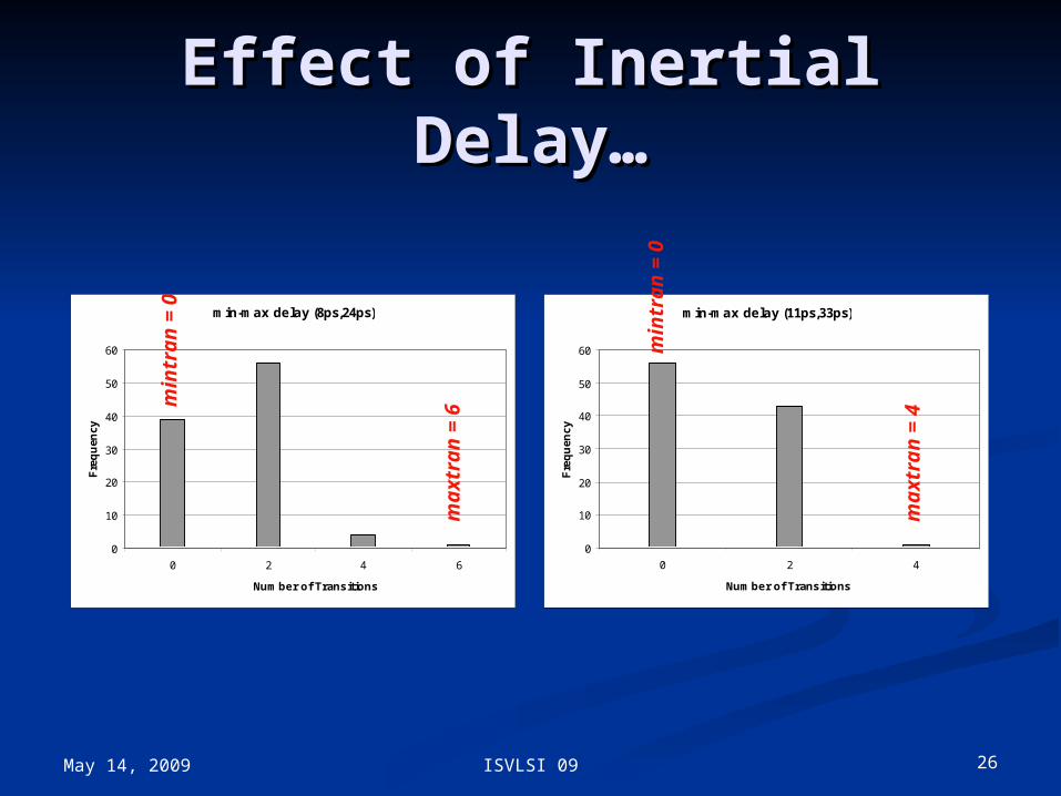
May 14, 2009 26ISVLSI 09
Effect of Inertial Delay…Effect of Inertial Delay…
min-max delay (8ps,24ps)
0
10
20
30
40
50
60
0 2 4 6
Number of Transitions
Fre
qu
ency
min-max delay (11ps,33ps)
0
10
20
30
40
50
60
0 2 4
Number of Transitions
Fre
qu
ency
min
tran
= 0
max
tran
= 6
min
tran
= 0
max
tran
= 4
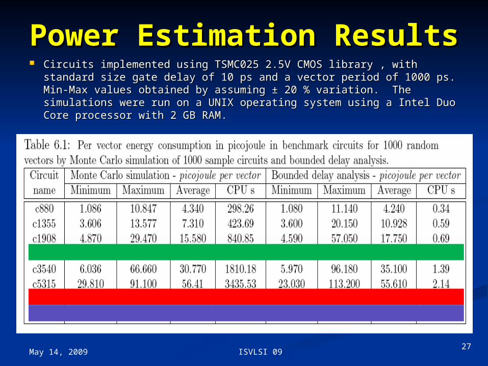
Power Estimation Power Estimation ResultsResults Circuits implemented using TSMC025 2.5V CMOS library , with standard Circuits implemented using TSMC025 2.5V CMOS library , with standard
size gate delay of 10 ps and a vector period of 1000 ps. Min-Max values size gate delay of 10 ps and a vector period of 1000 ps. Min-Max values obtained by assuming ± 20 % variation. The simulations were run on a obtained by assuming ± 20 % variation. The simulations were run on a UNIX operating system using a Intel Duo Core processor with 2 GB RAM.UNIX operating system using a Intel Duo Core processor with 2 GB RAM.
May 14, 2009 ISVLSI 09 27
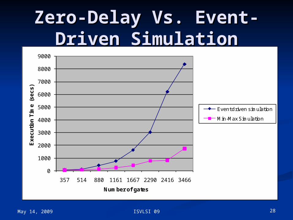
May 14, 2009 28ISVLSI 09
Zero-Delay Vs. Event-Zero-Delay Vs. Event-Driven SimulationDriven Simulation
0
1000
2000
3000
4000
5000
6000
7000
8000
9000
357 514 880 1161 1667 2290 2416 3466
Ex
ec
uti
on
Tim
e (
se
cs
)
Number of gates
Event driven simulation
Min-Max Simulation
May 14, 2009 29ISVLSI 09
ConclusionConclusion Bounded delay model allows power estimation Bounded delay model allows power estimation
method with consideration of uncertainties in method with consideration of uncertainties in
delays.delays.
Analysis has a linear time complexity in number Analysis has a linear time complexity in number
of gates and is an efficient alternative to the of gates and is an efficient alternative to the
Monte Carlo analysis.Monte Carlo analysis.
Monte Carlo versus min-max analysis: Reduced Monte Carlo versus min-max analysis: Reduced
dimension of sample space - Monte Carlo is over dimension of sample space - Monte Carlo is over
vectors and circuits;vectors and circuits; min-max is over vectors min-max is over vectors
only.only.
Future work: (a) Find number of vectors for Future work: (a) Find number of vectors for
convergence of result; (b) find probability convergence of result; (b) find probability
distribution of power.distribution of power.

May 14, 2009 30ISVLSI 09


