
EE141
1
EE141 EECS141 1 Lecture #5
EE141 EECS141 2 Lecture #5
Homework #2 posted First lab this week
EE141
2
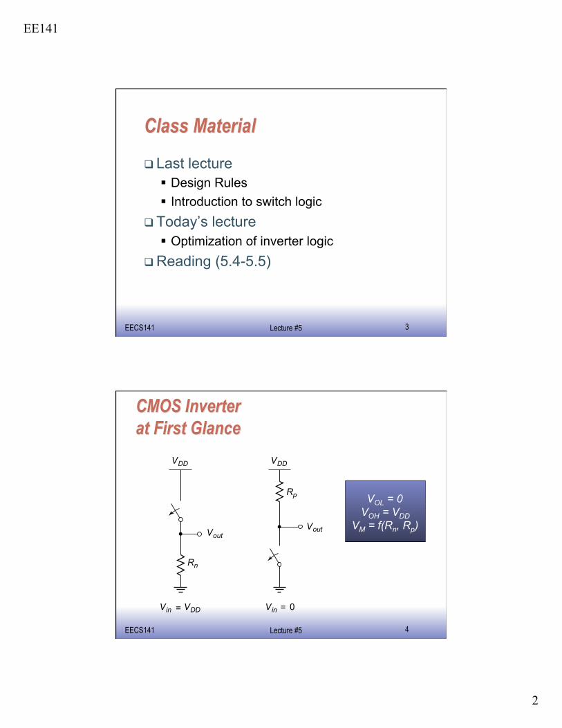
EE141 EECS141 3 Lecture #5
Last lecture Design Rules Introduction to switch logic
Today’s lecture Optimization of inverter logic
Reading (5.4-5.5)
EE141 EECS141 4 Lecture #5
VOL = 0 VOH = VDD
VM = f(Rn, Rp)
V DD V DD
V in = V DD V in = 0
V out V out
R n
R p

EE141
3
EE141 EECS141 5 Lecture #5
t pHL = f(RonCL) = 0.69 R n C L
(a) Low-to-high (b) High-to-low
EE141 EECS141 6 Lecture #5
CL
In Out
For some given CL: How many stages are needed to minimize delay? How to size the inverters?
Anyone want to guess the solution?

EE141
4
EE141 EECS141 7 Lecture #5
Get fastest delay if build one very big inverter So big that delay is set only by self-loading
Likely not the problem you’re interested in Someone has to drive this inverter…
EE141 EECS141 8 Lecture #5
Need to have a set of constraints
Constraints key to: Making the result useful Making the problem have a ‘clean’ solution
For sizing problem: Need to constrain size of first inverter
EE141
5
EE141 EECS141 9 Lecture #5
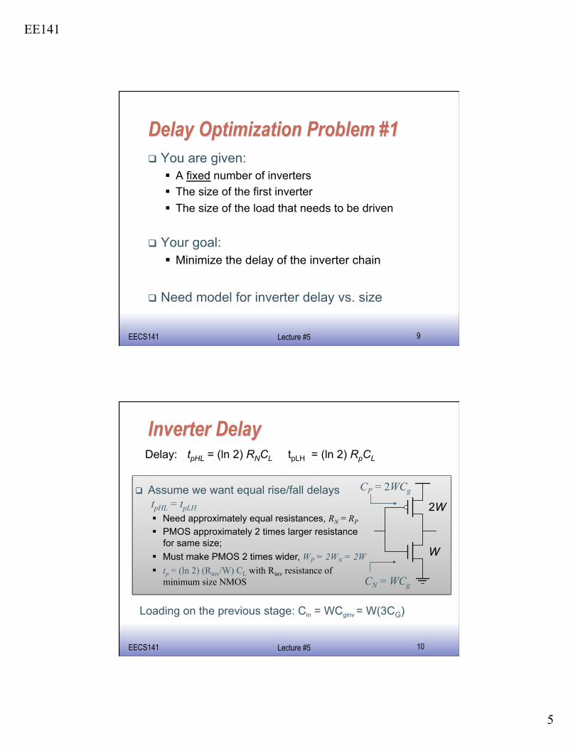
You are given: A fixed number of inverters The size of the first inverter The size of the load that needs to be driven
Your goal: Minimize the delay of the inverter chain
Need model for inverter delay vs. size
EE141 EECS141 10 Lecture #5
tpHL = (ln 2) RNCL tpLH = (ln 2) RpCL Delay:
2W
W
Assume we want equal rise/fall delays tpHL = tpLH Need approximately equal resistances, RN = RP
PMOS approximately 2 times larger resistance for same size;
Must make PMOS 2 times wider, WP = 2WN = 2W tp = (ln 2) (Rinv/W) CL with Rinv resistance of
minimum size NMOS
Loading on the previous stage: Cin = WCginv = W(3CG)
CP = 2WCg
CN = WCg

EE141
6
EE141 EECS141 11 Lecture #5
Cint CL
Replace ln(2) with k (a constant): Delay = kR(Cint + CL)
Delay = k(Rmin/W)(WCdinv + CL)
2W
W
R = Rinv/W Cint = W(3Cd) = WCdinv
EE141 EECS141 12 Lecture #5
Load
Delay
Delay = kR Cin(Cint/Cin+ CL /Cin) = kRminCginv[Cdinv/Cginv + CL/(WCginv)] = Delay (Internal) + Delay (Load) Cdinv/Cginv = γ = Constant independent of size
Cint CL
Cin 2W
W

EE141
7
EE141 EECS141 13 Lecture #5
Cint = γ Cin (γ ≈ 1 for CMOS inverter) f = CL/Cin – electrical fanout tinv = kRminCginv
tinv is independent of sizing of the gate!!!
EE141 EECS141 14 Lecture #5
CL
In Out
1 2 N
tp = tp1 + tp2 + …+ tpN

EE141
8
EE141 EECS141 15 Lecture #5
Delay equation has N-1 unknowns, Cin,2 … Cin,N
To minimize the delay, find N-1 partial derivatives:
EE141 EECS141 16 Lecture #5
Result: every stage has equal fanout:
In other words, size of each stage is geometric mean of two neighbors:
Equal fanout every stage will have same delay
EE141
9
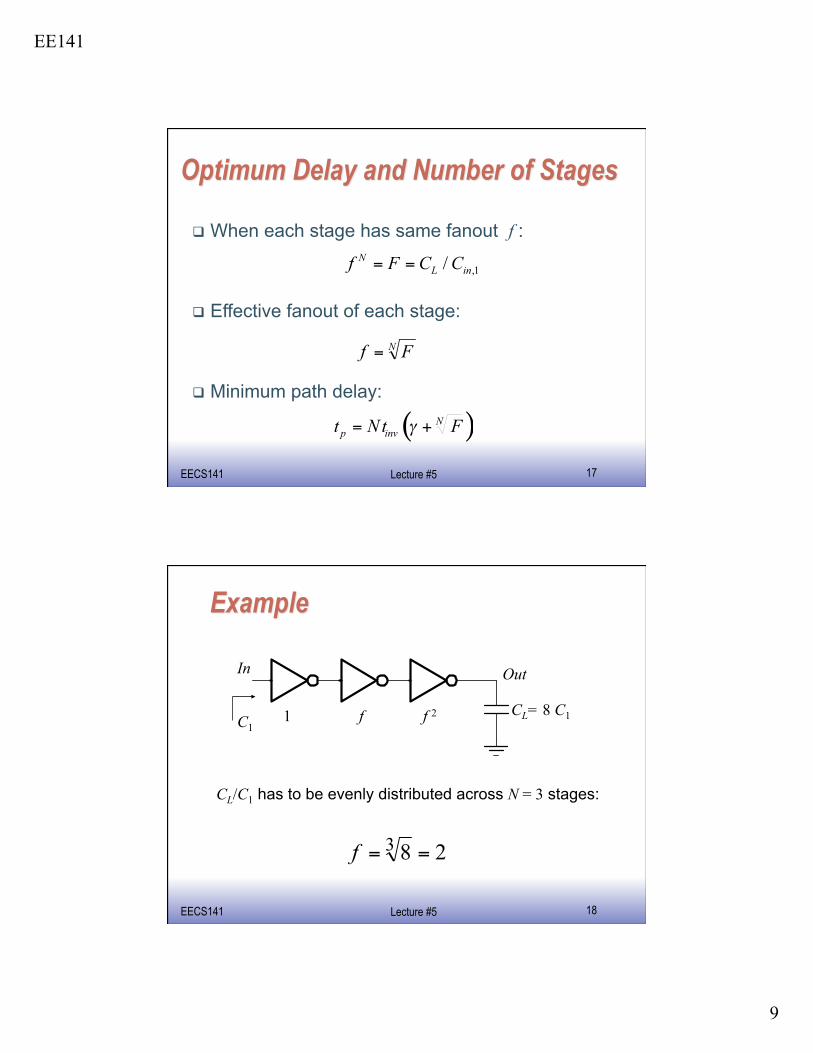
EE141 EECS141 17 Lecture #5
When each stage has same fanout f :
Effective fanout of each stage:
Minimum path delay:
EE141 EECS141 18 Lecture #5
CL= 8 C1
In Out
C1 1 f f 2
CL/C1 has to be evenly distributed across N = 3 stages:

EE141
10
EE141 EECS141 19 Lecture #5
You are given: The size of the first inverter The size of the load that needs to be driven
Your goal: Minimize delay by finding optimal number and
sizes of gates So, need to find N that minimizes:
EE141 EECS141 20 Lecture #5
For γ = 0, f = e, N = ln (CL/Cin)
Rewrite N in terms of fanout/stage f:

EE141
11
EE141 EECS141 21 Lecture #5
Optimum f for given process defined by γ
0 0.5 1 1.5 2 2.5 3 2.5
3
3.5
4
4.5
5
γ
f opt
fopt = 3.6 for γ = 1
e
EE141 EECS141 22 Lecture #5
Curves very flat for f > 2 Simplest/most common choice: f = 4
[Hodges, p.281]

EE141
12
EE141 EECS141 23 Lecture #5
Textbook: page 210 (γ = 1)
EE141 EECS141 24 Lecture #5
1
1
1
1
8
64
64
64
64
4
2.8 8
16
22.6
N f tp
1 64 65
2 8 18
3 4 15
4 2.8 15.3

EE141
13
EE141 EECS141 25 Lecture #5
Ignoring diffusion capacitance: Ctot = Cin + f·Cin + … + fN·Cin = Cin·(1 + f + … + fN) = Cin + Cin·fN + Cin·f·(1 + f + … + fN-2)
Overhead !!! f(fN-1-1) / (f-1)
Example (γ=0): CL = 20pF; Ci = 50fF → N = 6 Fixed: 20pF Overhead: 11.66pF !!!
EE141 EECS141 26 Lecture #5
Example: CL = 20pF; Cin = 50fF


