
Lecture 040 – Integrated Circuit Technology - II (5/11/03) Page 040-1
ECE 6440 - Frequency Synthesizers © P.E. Allen - 2003
LECTURE 040 – INTEGRATED CIRCUIT TECHNOLOGY - II(Reference [7,8])
ObjectiveThe objective of this presentation is:1.) Illustrate and model the passive components compatible with IC technology2.) The passive components examined will be those suitable for frequency synthesizersOutline• Resistors• Capacitors• Inductors• Summary
Lecture 040 – Integrated Circuit Technology - II (5/11/03) Page 040-2
ECE 6440 - Frequency Synthesizers © P.E. Allen - 2003
RESISTORSMOS Resistors - Source/Drain Resistor
p- substrate
FOX FOX
SiO2
Metal
n- well
p+
Fig. 2.5-16
Diffusion:10-100 ohms/squareAbsolute accuracy = ±35%Relative accuracy=2% (5µm), 0.2% (50µm)Temperature coefficient = +1500 ppm/°CVoltage coefficient ≈ 200 ppm/V
Ion Implanted:500-2000 ohms/squareAbsolute accuracy = ±15%Relative accuracy=2% (5µm), 0.15% (50µmTemperature coefficient = +400 ppm/°CVoltage coefficient ≈ 800 ppm/V
Comments:• Parasitic capacitance to substrate is voltage dependent.• Piezoresistance effects occur due to chip strain from mounting.
Lecture 040 – Integrated Circuit Technology - II (5/11/03) Page 040-3
ECE 6440 - Frequency Synthesizers © P.E. Allen - 2003
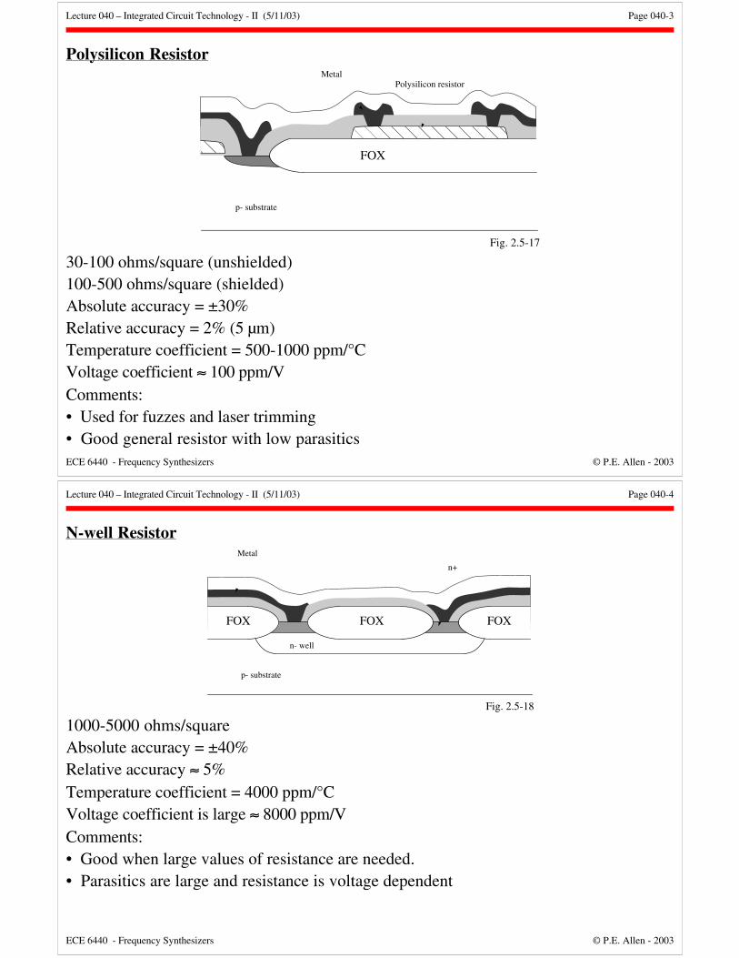
Polysilicon Resistor
Fig. 2.5-17
p- substrate
FOX
Polysilicon resistorMetal
30-100 ohms/square (unshielded)100-500 ohms/square (shielded)Absolute accuracy = ±30%Relative accuracy = 2% (5 µm)Temperature coefficient = 500-1000 ppm/°CVoltage coefficient ≈ 100 ppm/VComments:• Used for fuzzes and laser trimming• Good general resistor with low parasitics
Lecture 040 – Integrated Circuit Technology - II (5/11/03) Page 040-4
ECE 6440 - Frequency Synthesizers © P.E. Allen - 2003
N-well Resistor
Fig. 2.5-18
p- substrate
FOX FOX
Metal
n- well
n+
FOX
1000-5000 ohms/squareAbsolute accuracy = ±40%Relative accuracy ≈ 5%Temperature coefficient = 4000 ppm/°CVoltage coefficient is large ≈ 8000 ppm/VComments:• Good when large values of resistance are needed.• Parasitics are large and resistance is voltage dependent
Lecture 040 – Integrated Circuit Technology - II (5/11/03) Page 040-5
ECE 6440 - Frequency Synthesizers © P.E. Allen - 2003
CAPACITORSTypes of Capacitors Considered• pn junction capacitors• Standard MOS capacitors• Accumulation mode MOS capacitors• Poly-poly capacitors• Metal-metal capacitors
Characterization of CapacitorsAssume C is the desired capacitance:1.) Dissipation (quality factor) of a capacitor is
Q = ωCRp
where Rp is the equivalent resistance in parallel with the capacitor, C.
2.) Cmax/Cmin ratio is the ratio of the largest value of capacitance to the smallest whenthe capacitor is used as a variable capacitor called varactor.
3.) Variation of capacitance with the control voltage.4.) Parasitic capacitors from both terminal of the desired capacitor to ac ground.
Lecture 040 – Integrated Circuit Technology - II (5/11/03) Page 040-6
ECE 6440 - Frequency Synthesizers © P.E. Allen - 2003
Desirable Characteristics of Varactors1.) A high quality factor2.) A control voltage range compatible with supply voltage3.) Good tunability over the available control voltage range4.) Small silicon area (reduces cost)5.) Reasonably uniform capacitance variation over the available control voltage range6.) A high Cmax/Cmin ratio
Some References for Further Information1.) P. Andreani and S. Mattisson, “On the Use of MOS Varactors in RF VCO’s,” IEEEJ. of Solid-State Circuits, vol. 35, no. 6, June 2000, pp. 905-910.2.) A-S Porret, T. Melly, C. Enz, and E. Vittoz, “Design of High-Q Varactors for Low-Power Wireless Applications Using a Standard CMOS Process,” IEEE J. of Solid-StateCircuits, vol. 35, no. 3, March 2000, pp. 337-345.3.) E. Pedersen, “RF CMOS Varactors for 2GHz Applications,” Analog IntegratedCircuits and Signal Processing, vol. 26, pp. 27-36, Jan. 2001

Lecture 040 – Integrated Circuit Technology - II (5/11/03) Page 040-7
ECE 6440 - Frequency Synthesizers © P.E. Allen - 2003
PN Junction CapacitorsGenerally made by diffusion into the well.
Anode
n-well
p+
Substrate
Fig. 2.5-011
n+n+
p+
DepletionRegion
Cathode
p- substrate
CjCj
RwjRwj Rw
Cw
Rs
Anode Cathode
VA VBC
Rwj
rD
Layout:
Minimize the distance between the p+ and n+ diffusions.Two different versions have been tested.
1.) Large islands – 9µm on a side2.) Small islands – 1.2µm on a side n-well
n+ diffusion
p+ dif-fusion
Fig. 2.5-1A
Lecture 040 – Integrated Circuit Technology - II (5/11/03) Page 040-8
ECE 6440 - Frequency Synthesizers © P.E. Allen - 2003
PN-Junction Capacitors – ContinuedThe anode should be the floating node and the cathode must be connected to ac ground.Experimental data (Q at 2GHz, 0.5µm CMOS):
00.5
1
1.52
2.5
3
3.54
0 0.5 1 1.5 2 2.5 3 3.5
CA
node
(pF
)
Cathode Voltage (V)
Large Islands
Small Islands
Cmax Cmin
0
20
40
60
80
100
120
0 0.5 1 1.5 2 2.5 3 3.5
QA
node
Qmin Qmax
Large Islands
Small Islands
Fig2.5-1BCathode Voltage (V)
Summary:
Small Islands (598 1.2µm x1.2µm) Large Islands (42 9µm x 9µm)TerminalUnder Test Cmax/Cmin Qmin Qmax Cmax/Cmin Qmin Qmax
Anode 1.23 94.5 109 1.32 19 22.6Cathode 1.21 8.4 9.2 1.29 8.6 9.5
Electrons as majority carriers lead to higher Q because of their higher mobility.The resistance, Rwj, is reduced in small islands compared with large islands ⇒ higher Q.
Lecture 040 – Integrated Circuit Technology - II (5/11/03) Page 040-9
ECE 6440 - Frequency Synthesizers © P.E. Allen - 2003
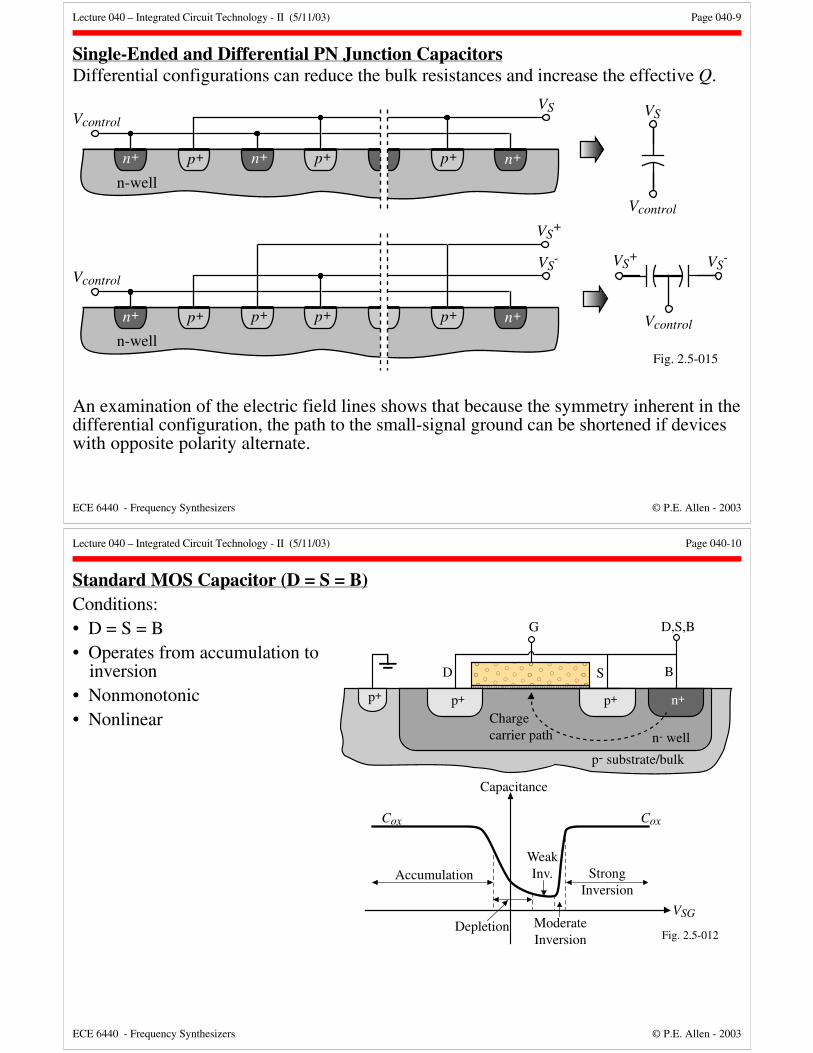
Single-Ended and Differential PN Junction CapacitorsDifferential configurations can reduce the bulk resistances and increase the effective Q.
VcontrolVS
n+ p+ n+ p+ p+ n+
n-well
VcontrolVS
-
n+ p+ p+ p+ p+ n+
n-well
VS+
VS
Vcontrol
VS+ VS
-
Vcontrol
Fig. 2.5-015
An examination of the electric field lines shows that because the symmetry inherent in thedifferential configuration, the path to the small-signal ground can be shortened if deviceswith opposite polarity alternate.
Lecture 040 – Integrated Circuit Technology - II (5/11/03) Page 040-10
ECE 6440 - Frequency Synthesizers © P.E. Allen - 2003
Standard MOS Capacitor (D = S = B)Conditions:• D = S = B• Operates from accumulation to
inversion• Nonmonotonic• Nonlinear p+
B
G D,S,B
p- substrate/bulk
p+p+
Fig. 2.5-012
n- well
n+
D S
VSG
Capacitance
StrongInversion
Accumulation
ModerateInversion
WeakInv.
Depletion
CoxCox
Charge carrier path
Lecture 040 – Integrated Circuit Technology - II (5/11/03) Page 040-11
ECE 6440 - Frequency Synthesizers © P.E. Allen - 2003
Inversion Mode MOS CapacitorsConditions:• D = S, B = VDD
• Accumulation region removedby connecting bulk to VDD
• Channel resistance:
Ron = L
12KP'(VBG-|VT|)
• LDD transistors will givelower Q because of theincreased series resistance
p+
B
G D,S
p- substrate/bulk
p+p+
Fig. 2.5-013
n- well
n+
D S
VSG
Capacitance
CoxCox
VDD
0
VT shift dueto VBS
p-channel
Charge carrier paths
B = D = S
InversionMode MOS
Lecture 040 – Integrated Circuit Technology - II (5/11/03) Page 040-12
ECE 6440 - Frequency Synthesizers © P.E. Allen - 2003
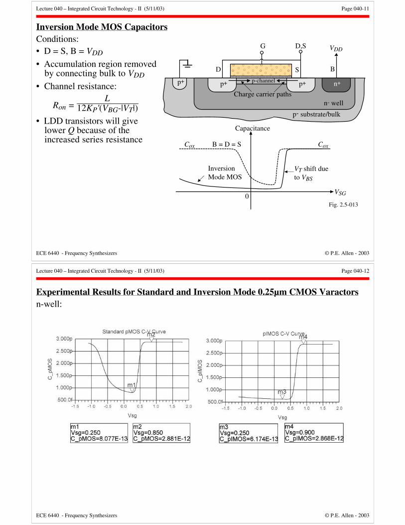
Experimental Results for Standard and Inversion Mode 0.25µm CMOS Varactorsn-well:

Lecture 040 – Integrated Circuit Technology - II (5/11/03) Page 040-13
ECE 6440 - Frequency Synthesizers © P.E. Allen - 2003
Inversion Mode MOS Capacitors – ContinuedBulk tuning of the polysilicon-oxide-channel capacitor (0.35µm CMOS)
-0.65V
vBCG
1.0
0.8
0.6
0.4
0.20.0
-0.5-0.6-0.7-0.8-0.9-1.0-1.1-1.3-1.4-1.5 -1.2
CG
VT
vB (Volts)
Vol
ts o
r pF
Fig. 2.5-3
Cmax/Cmin ≈ 4
Interpretation:
Fig. 2.5-34
VSG
CapacitanceCox
0
InversionMode MOS
0.65V
Cmax
Cmin
VBS = -1.50VVBS = -1.05VVBS = -0.65V
Lecture 040 – Integrated Circuit Technology - II (5/11/03) Page 040-14
ECE 6440 - Frequency Synthesizers © P.E. Allen - 2003
Inversion Mode NMOS Varactor – ContinuedMore Detail - Includes the LDD transistor
Cox
p+
Bulk
G D,S
G
D,S
p- substrate/bulkn+n+
n- LDD
Rd RdCd CdCsi
CjRsj
Rsi
Cov Cov B
Fig. 2.5-2
Shown in inversion mode
Best results are obtained when the drain-source are on ac ground.Experimental Results (Q at 2GHz, 0.5µm CMOS):
1.5
2
2.5
3
3.5
4
4.5
0 0.5 1 1.5 2 2.5 3 3.5
CG
ate
(pF)
VG = 2.1V
VG = 1.8V
VG = 1.5V
Cmax Cmin
Drain/Source Voltage (V)
2224
26
2830
32
34
3638
0 0.5 1 1.5 2 2.5 3 3.5
VG = 2.1V
VG = 1.8V
VG = 1.5V
Qmax Qmin
Drain/Source Voltage (V) Fig. 2.5-1c
QG
ate
VG =1.8V: Cmax/Cmin ratio = 2.15 (1.91), Qmax = 34.3 (5.4), and Qmin = 25.8(4.9)
Lecture 040 – Integrated Circuit Technology - II (5/11/03) Page 040-15
ECE 6440 - Frequency Synthesizers © P.E. Allen - 2003
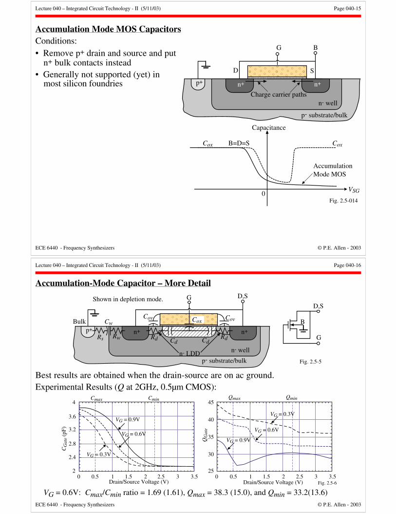
Accumulation Mode MOS CapacitorsConditions:• Remove p+ drain and source and put
n+ bulk contacts instead• Generally not supported (yet) in
most silicon foundries p+
G B
p- substrate/bulk
n+
Fig. 2.5-014
n- well
n+
D S
VSG
Capacitance
CoxCox
0
Charge carrier paths
B=D=S
AccumulationMode MOS
Lecture 040 – Integrated Circuit Technology - II (5/11/03) Page 040-16
ECE 6440 - Frequency Synthesizers © P.E. Allen - 2003
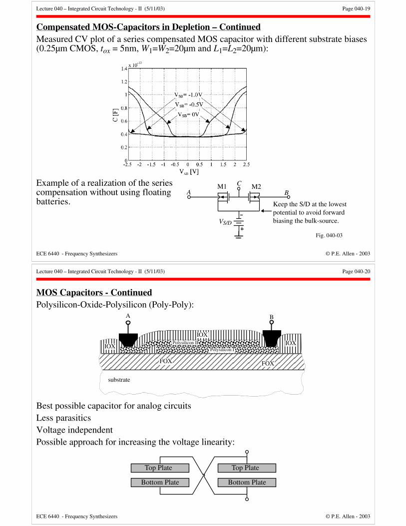
Accumulation-Mode Capacitor – More Detail
Cox
p+Bulk
G D,S
G
D,S
p- substrate/bulk
n+n+
n- LDD
Rd RdCd Cd
Cw
Rs
Cov Cov B
Fig. 2.5-5
n- well
Rw
Shown in depletion mode.
Best results are obtained when the drain-source are on ac ground.Experimental Results (Q at 2GHz, 0.5µm CMOS):
2
2.4
2.8
3.2
3.6
4
0 0.5 1 1.5 2 2.5 3 3.5
CG
ate
(pF)
VG = 0.9V
VG = 0.6V
VG = 0.3V
Cmax Cmin
Drain/Source Voltage (V)
25
30
35
40
45
0 0.5 1 1.5 2 2.5 3 3.5
Qmax Qmin
Drain/Source Voltage (V)
QG
ate
VG = 0.9V
VG = 0.6V
VG = 0.3V
Fig. 2.5-6
VG = 0.6V: Cmax/Cmin ratio = 1.69 (1.61), Qmax = 38.3 (15.0), and Qmin = 33.2(13.6)

Lecture 040 – Integrated Circuit Technology - II (5/11/03) Page 040-17
ECE 6440 - Frequency Synthesizers © P.E. Allen - 2003
Differential Varactors†
Vcontrol
A B
Vcontrol
A B
VDD
Vcontrol
A B
Diode Varactor Inversion-PMOS Varactor Accumulation-PMOS VaractorFig. 040-01
† P. Andreani and S. Mattisson, “On the Use of MOS Varactors in RF VCO’s,” IEEE J. of Solid-State Circuits, Vol. 35, No. 6, June 2000, pp. 905-
910.
Varactor fL –fH(GHz)
fC(GHz)
TuningRange
Diode 1.73-1.93
1.83 10.9%
I-MOS 1.71-1.91
1.81 11.0%
A-MOS 1.70-1.89
1.80 10.6%
Lecture 040 – Integrated Circuit Technology - II (5/11/03) Page 040-18
ECE 6440 - Frequency Synthesizers © P.E. Allen - 2003
Compensated MOS-Capacitors in Depletion with Substrate Biasing†
Substrate biasing keeps the MOS capacitors in a broad depletion region and extends theusable voltage range and achieves a first-order cancellation of the nonlinearity effect.Principle:
† T. Tille, J. Sauerbrey and D. Schmitt-Landsiedel, “A 1.8V MOSFET-Only Σ∆ Modulator Using Substrate Biased Depletion-Mode MOS Capacitors
in Series Compensation,” IEEE J. of Solid-State Circuits, Vol. 36, No. 7, July 2001, pp. 1041-1047.
A BC
VSB1 VSB2
M1 M2
Fig. 040-02
Lecture 040 – Integrated Circuit Technology - II (5/11/03) Page 040-19
ECE 6440 - Frequency Synthesizers © P.E. Allen - 2003
Compensated MOS-Capacitors in Depletion – ContinuedMeasured CV plot of a series compensated MOS capacitor with different substrate biases(0.25µm CMOS, tox = 5nm, W1=W2=20µm and L1=L2=20µm):
Example of a realization of the seriescompensation without using floatingbatteries.
A BC
VS/D
M1 M2
Fig. 040-03
Keep the S/D at the lowestpotential to avoid forwardbiasing the bulk-source.
Lecture 040 – Integrated Circuit Technology - II (5/11/03) Page 040-20
ECE 6440 - Frequency Synthesizers © P.E. Allen - 2003
MOS Capacitors - ContinuedPolysilicon-Oxide-Polysilicon (Poly-Poly):
substrate
IOXIOX
A B
IOX
FOX FOX
Polysilicon II
Polysilicon I
Best possible capacitor for analog circuitsLess parasiticsVoltage independentPossible approach for increasing the voltage linearity:
Top Plate
Bottom Plate
Top Plate
Bottom Plate

Lecture 040 – Integrated Circuit Technology - II (5/11/03) Page 040-21
ECE 6440 - Frequency Synthesizers © P.E. Allen - 2003
Implementation of Capacitors using Available Interconnect Layers
T
B
M3M2
M1T B
M3M2
M1PolyB
T
M2M1
PolyB T
M2M1
BT
Fig. 2.5-8
Much more information on using metal for capacitance is found in the reference: R.Aparicio and A. Hamimiri, “Capacity Limits and Matching Properties of IntegratedCapacitors,” IEEE J. of Solid-State Circuits, Vol. 37, No. 3, March 2002, pp. 384-393.
Lecture 040 – Integrated Circuit Technology - II (5/11/03) Page 040-22
ECE 6440 - Frequency Synthesizers © P.E. Allen - 2003
Horizontal Metal CapacitorsCapacitance between conductors on the same level and use lateral flux.
These capacitors are sometimes called fractal capacitors because the fractal patterns arestructures that enclose a finite area with an infinite perimeter.The capacitor/area can be increased by a factor of 10 over vertical flux capacitors.
+ - + -
+ - +-
Fringing field
Metal
Fig2.5-9
+ - + -Metal 3
Metal 2
Metal 1
Metal
Top view:
Side view:
Lecture 040 – Integrated Circuit Technology - II (5/11/03) Page 040-23
ECE 6440 - Frequency Synthesizers © P.E. Allen - 2003
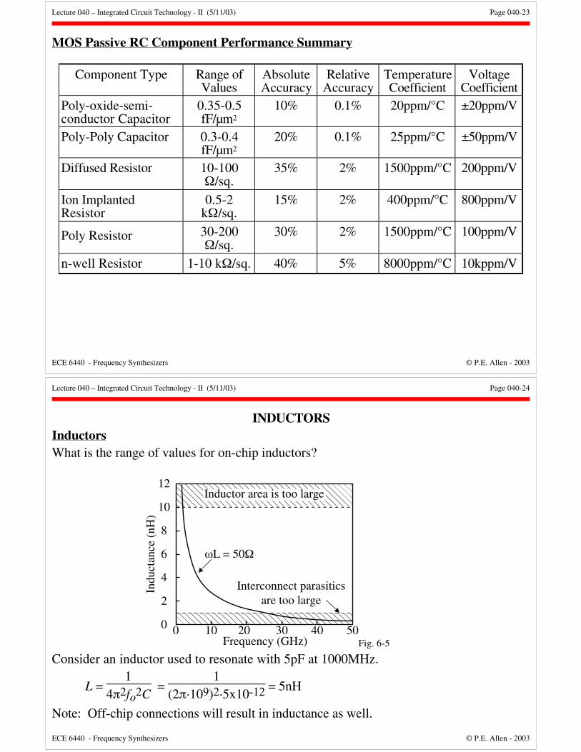
MOS Passive RC Component Performance Summary
Component Type Range ofValues
AbsoluteAccuracy
RelativeAccuracy
TemperatureCoefficient
VoltageCoefficient
Poly-oxide-semi-conductor Capacitor
0.35-0.5fF/µm2
10% 0.1% 20ppm/°C ±20ppm/V
Poly-Poly Capacitor 0.3-0.4fF/µm2
20% 0.1% 25ppm/°C ±50ppm/V
Diffused Resistor 10-100Ω/sq.
35% 2% 1500ppm/°C 200ppm/V
Ion ImplantedResistor
0.5-2kΩ/sq.
15% 2% 400ppm/°C 800ppm/V
Poly Resistor 30-200Ω/sq.
30% 2% 1500ppm/°C 100ppm/V
n-well Resistor 1-10 kΩ/sq. 40% 5% 8000ppm/°C 10kppm/V
Lecture 040 – Integrated Circuit Technology - II (5/11/03) Page 040-24
ECE 6440 - Frequency Synthesizers © P.E. Allen - 2003
INDUCTORSInductorsWhat is the range of values for on-chip inductors?
0 10 20 30 40 50
12
10
8
6
4
2
0Frequency (GHz)
Indu
ctan
ce (
nH)
ωL = 50Ω
Inductor area is too large
Interconnect parasiticsare too large
Fig. 6-5
Consider an inductor used to resonate with 5pF at 1000MHz.
L = 1
4π2fo2C =
1(2π·109)2·5x10-12 = 5nH
Note: Off-chip connections will result in inductance as well.
Lecture 040 – Integrated Circuit Technology - II (5/11/03) Page 040-25
ECE 6440 - Frequency Synthesizers © P.E. Allen - 2003
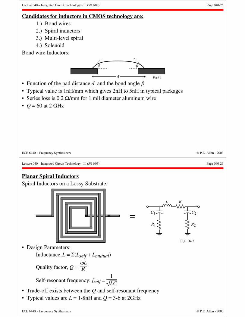
Candidates for inductors in CMOS technology are:1.) Bond wires2.) Spiral inductors3.) Multi-level spiral4.) Solenoid
Bond wire Inductors:
β β
d Fig.6-6
• Function of the pad distance d and the bond angle β• Typical value is 1nH/mm which gives 2nH to 5nH in typical packages• Series loss is 0.2 Ω/mm for 1 mil diameter aluminum wire• Q ≈ 60 at 2 GHz
Lecture 040 – Integrated Circuit Technology - II (5/11/03) Page 040-26
ECE 6440 - Frequency Synthesizers © P.E. Allen - 2003
Planar Spiral InductorsSpiral Inductors on a Lossy Substrate:
C1
L R
C2
R2R1
Fig. 16-7
• Design Parameters:Inductance,L = Σ(Lself + Lmutual)
Quality factor, Q = ωLR
Self-resonant frequency: fself = 1LC
• Trade-off exists between the Q and self-resonant frequency• Typical values are L = 1-8nH and Q = 3-6 at 2GHz

Lecture 040 – Integrated Circuit Technology - II (5/11/03) Page 040-27
ECE 6440 - Frequency Synthesizers © P.E. Allen - 2003
Planar Spiral Inductors - ContinuedInductor Design
I
I
I
I
W
S
ID
Nturns = 2.5
SiO2
Silicon
Fig. 6-9
Typically: 3 < Nturns < 5 and S = Smin for the given current
Select the OD, Nturns, and W so that ID allows sufficient magnetic flux to flowthrough the center.Loss Mechanisms:• Skin effect• Capacitive substrate losses• Eddy currents in the silicon
Lecture 040 – Integrated Circuit Technology - II (5/11/03) Page 040-28
ECE 6440 - Frequency Synthesizers © P.E. Allen - 2003
Planar Spiral Inductors - ContinuedInfluence of a Lossy Substrate
C1
L R
C2
R2R1
Fig. 12.2-13
CLoad
where:L is the desired inductanceR is the series resistanceC1 and C2 are the capacitance from the inductor to the ground plane
R1 and R2 are the eddy current losses in the silicon
Guidelines for using spiral inductors on chip:• Lossy substrate degrades Q at frequencies close to fself• To achieve an inductor, one must select frequencies less than fself• The Q of the capacitors associated with the inductor should be very high
Lecture 040 – Integrated Circuit Technology - II (5/11/03) Page 040-29
ECE 6440 - Frequency Synthesizers © P.E. Allen - 2003
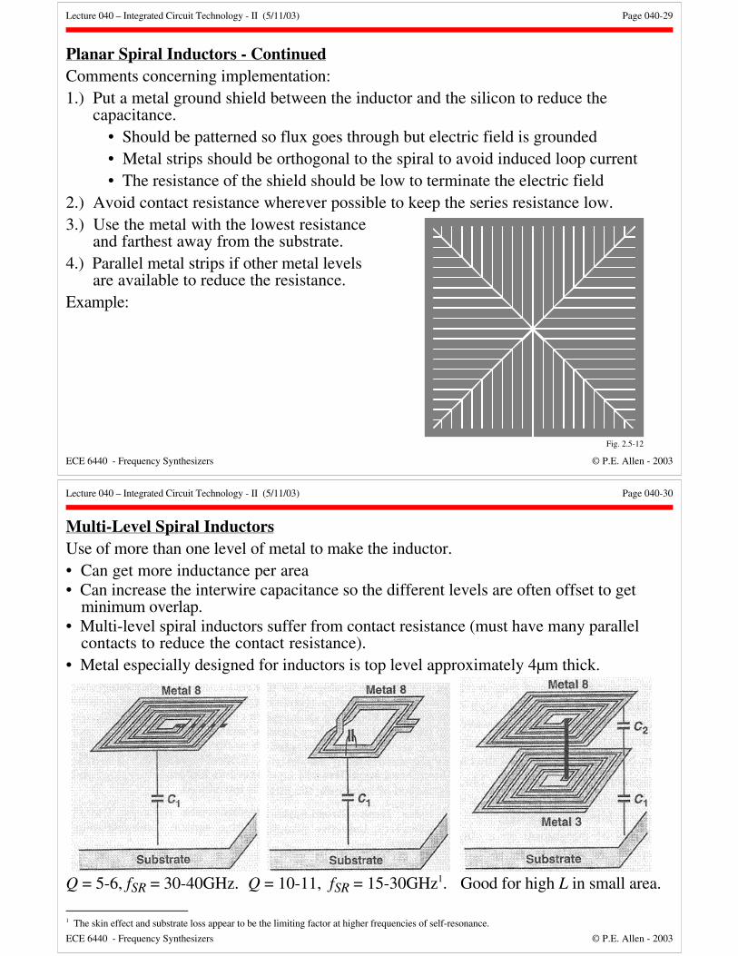
Planar Spiral Inductors - ContinuedComments concerning implementation:1.) Put a metal ground shield between the inductor and the silicon to reduce the
capacitance.• Should be patterned so flux goes through but electric field is grounded• Metal strips should be orthogonal to the spiral to avoid induced loop current• The resistance of the shield should be low to terminate the electric field
2.) Avoid contact resistance wherever possible to keep the series resistance low.3.) Use the metal with the lowest resistance
and farthest away from the substrate.4.) Parallel metal strips if other metal levels
are available to reduce the resistance.Example:
Fig. 2.5-12
Lecture 040 – Integrated Circuit Technology - II (5/11/03) Page 040-30
ECE 6440 - Frequency Synthesizers © P.E. Allen - 2003
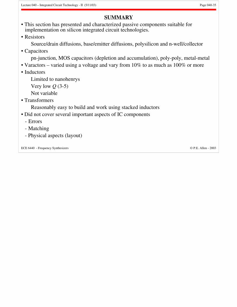
Multi-Level Spiral InductorsUse of more than one level of metal to make the inductor.• Can get more inductance per area• Can increase the interwire capacitance so the different levels are often offset to get
minimum overlap.• Multi-level spiral inductors suffer from contact resistance (must have many parallel
contacts to reduce the contact resistance).• Metal especially designed for inductors is top level approximately 4µm thick.
Q = 5-6, fSR = 30-40GHz. Q = 10-11, fSR = 15-30GHz1. Good for high L in small area.
1 The skin effect and substrate loss appear to be the limiting factor at higher frequencies of self-resonance.

Lecture 040 – Integrated Circuit Technology - II (5/11/03) Page 040-31
ECE 6440 - Frequency Synthesizers © P.E. Allen - 2003
Inductors - ContinuedSelf-resonance as a function of inductance. Outer dimension of inductors.
Lecture 040 – Integrated Circuit Technology - II (5/11/03) Page 040-32
ECE 6440 - Frequency Synthesizers © P.E. Allen - 2003
Solenoid InductorsExample:
Coil Current
Magnetic Flux
Coil CurrentUpper Metal
Lower Metal
ContactVias
Silicon
SiO2
Fig. 6-11
Comments:• Magnetic flux is small due to planar structure• Capacitive coupling to substrate is still present• Potentially best with a ferromagnetic core

Lecture 040 – Integrated Circuit Technology - II (5/11/03) Page 040-33
ECE 6440 - Frequency Synthesizers © P.E. Allen - 2003
TransformersTransformer structures are easily obtained using stacked inductors as shown below for a1:2 transformer.
Method of reducing theinterwinding capacitances.
4 turns 8 turns 3 turns
Measured 1:2 transformer voltage gains:
Lecture 040 – Integrated Circuit Technology - II (5/11/03) Page 040-34
ECE 6440 - Frequency Synthesizers © P.E. Allen - 2003
Transformers – ContinuedA 1:4 transformer:Structure- Measured voltage gain-
(CL = 0, 50fF, 100fF, 500fF and 1pF.CL is the capacitive loading on thesecondary.)
Secondary
Lecture 040 – Integrated Circuit Technology - II (5/11/03) Page 040-35
ECE 6440 - Frequency Synthesizers © P.E. Allen - 2003
SUMMARY• This section has presented and characterized passive components suitable for
implementation on silicon integrated circuit technologies.• Resistors
Source/drain diffusions, base/emitter diffusions, polysilicon and n-well/collector• Capacitors
pn-junction, MOS capacitors (depletion and accumulation), poly-poly, metal-metal• Varactors – varied using a voltage and vary from 10% to as much as 100% or more• Inductors
Limited to nanohenrysVery low Q (3-5)Not variable
• TransformersReasonably easy to build and work using stacked inductors
• Did not cover several important aspects of IC components- Errors- Matching- Physical aspects (layout)


