
InvenSense Inc. 1197 Borregas Ave, Sunnyvale, CA 94089 U.S.A. Tel: +1 (408) 988-7339 Fax: +1 (408) 988-8104
Website: www.invensense.com
Document Number: RM-ITG-3200A-00 Revision: 1.0 Release Date: 06/06/2011
ITG-3200 Register Map & Register Descriptions
Revision 1.0

ITG-3200 Register Map
Document Number: RM-ITG-3200A-00 Revision: 1.0 Release Date: 06/06/2011
2 of 13
CONTENTS
1 DOCUMENT INFORMATION .............................................................................................................................. 3
1.1 REVISION HISTORY ............................................................................................................................................. 3 1.2 PURPOSE AND SCOPE ........................................................................................................................................... 4 1.3 PRODUCT OVERVIEW .......................................................................................................................................... 4 1.4 SOFTWARE SOLUTIONS........................................................................................................................................ 4
2 REGISTER MAP ..................................................................................................................................................... 6
3 REGISTER DESCRIPTION ................................................................................................................................... 7
3.1 REGISTER 0 – WHO AM I ..................................................................................................................................... 7 3.2 REGISTER 21 – SAMPLE RATE DIVIDER ............................................................................................................... 7 3.3 REGISTER 22 – DLPF, FULL SCALE ..................................................................................................................... 8 3.4 REGISTER 23 – INTERRUPT CONFIGURATION ......................................................................................................10 3.5 REGISTER 26 – INTERRUPT STATUS ....................................................................................................................10 3.6 REGISTERS 27 TO 34 – SENSOR REGISTERS.........................................................................................................11 3.7 REGISTER 62 – POWER MANAGEMENT ...............................................................................................................11

ITG-3200 Register Map
Document Number: RM-ITG-3200A-00 Revision: 1.0 Release Date: 06/06/2011
3 of 13
1 Document Information
1.1 Revision History
Revision Date Revision Description
06/06/11 1.0 Initial Release Separated Register Map and Register Descriptions from Product Spec Sec. 3.1 Clarified bit0

ITG-3200 Register Map
Document Number: RM-ITG-3200A-00 Revision: 1.0 Release Date: 06/06/2011
4 of 13
1.2 Purpose and Scope This document provides information regarding the register map and register descriptions for the ITG-3200
TM.
1.3 Product Overview The ITG-3200 is the world’s first single-chip, digital-output, 3-axis MEMS gyro IC optimized for gaming, 3D mice, and 3D remote control applications. The part features enhanced bias and sensitivity temperature stability, reducing the need for user calibration. Low frequency noise is lower than previous generation devices, simplifying application development and making for more-responsive remote controls.
The ITG-3200 features three 16-bit analog-to-digital converters (ADCs) for digitizing the gyro outputs, a user-selectable internal low-pass filter bandwidth, and a Fast-Mode I
2C (400kHz) interface. Additional features
include an embedded temperature sensor and a 2% accurate internal oscillator. This breakthrough in gyroscope technology provides a dramatic 67% package size reduction, delivers a 50% power reduction, and has inherent cost advantages compared to competing multi-chip gyro solutions.
By leveraging its patented and volume-proven Nasiri-Fabrication platform, which integrates MEMS wafers with companion CMOS electronics through wafer-level bonding, InvenSense has driven the ITG-3200 package size down to a revolutionary footprint of 4x4x0.9mm (QFN), while providing the highest performance, lowest noise, and the lowest cost semiconductor packaging required for handheld consumer electronic devices. The part features a robust 10,000g shock tolerance, as required by portable consumer equipment.
For power supply flexibility, the ITG-3200 has a separate VLOGIC reference pin, in addition to its analog supply pin, VDD, which sets the logic levels of its I
2C interface. The VLOGIC voltage may be anywhere from
1.71V min to VDD max.
1.4 Software Solutions This section describes the MotionApps™ software solutions included with the InvenSense MPU™ (MotionProcessing Unit™) and IMU (Inertial Measurement Unit) product families. Please note that the products within the IDG, IXZ, and ITG families do not include these software solutions.
The MotionApps Platform is a complete software solution that in combination with the InvenSense IMU and MPU MotionProcessor™ families delivers robust, well-calibrated 6-axis and/or 9-axis sensor fusion data using its field proven and proprietary MotionFusion™ engine. Solution packages are available for smartphones and tablets as well as for embedded microcontroller-based devices.
The MotionApps Platform provides a turn-key solution for developers and accelerates time-to-market. It consists of complex 6/9-axis sensor fusion algorithms, robust multi-sensor calibration, a proven software architecture for Android and other leading operating systems, and a flexible power management scheme.
The MotionApps Platform is integrated within the middleware of the target OS (the sensor framework), and also provides a kernel device driver to interface with the physical device. This directly benefits application developers by providing a cohesive set of APIs and a well-defined sensor data path in the user-space.

ITG-3200 Register Map
Document Number: RM-ITG-3200A-00 Revision: 1.0 Release Date: 06/06/2011
5 of 13
The table below describes the MotionApps software solutions included with the InvenSense MPU and IMU product families.
InvenSense MotionProcessor Devices and Included MotionApps Software
Included Software
Feature MotionApps Embedded
MotionApps MotionApps
Lite
Embedded MotionApps
Lite Notes
Part Number MPU-3050™ MPU-6050™
IMU-3000™
Processor Type Mobile
Application Processor
8/16/32-bit Microcontroller
Mobile Application Processor
8/16/32-bit Microcontroller
Applications Smartphones,
tablets
TV remotes, health/fitness,
toys, other embedded
Smartphones, tablets
TV remotes, health/fitness,
toys, other embedded
6-Axis MotionFusion Yes Yes
< 2% Application Processor load using on-chip Digital Motion Processor (DMP).
Reduces processing requirements for embedded applications
9-Axis MotionFusion Yes No
Gyro Bias Calibration Yes Yes No-Motion calibration and temperature calibration
3rd
Party Compass Cal API
Yes No Integrates 3
rd party compass
libraries
Gyro-Assisted Compass Calibration (Fast Heading)
Yes No Quick compass calibration using gyroscope
Magnetic Anomaly Rejection (Improved Heading)
Yes No Uses gyro heading data when magnetic anomaly is detected
The table below lists recommended documentation for the MotionApps software solutions.
Software Documentation
Platform MotionApps and MotionApps Lite Embedded MotionApps and Embedded MotionApps Lite
Software Documentation
Installation Guide for Linux and Android MotionApps Platform, v1.9 or later
Embedded MotionApps Platform User Guide, v3.0 or later
MPL Functional Specifications Embedded MPL Functional Specifications
For more information about the InvenSense MotionApps Platform, please visit the Developer’s Corner or consult your local InvenSense Sales Representative.

ITG-3200 Register Map
Document Number: RM-ITG-3200A-00 Revision: 1.0 Release Date: 06/06/2011
6 of 13
2 Register Map
Addr
Hex
Addr
Decimal Register Name R/W Bit7 Bit6 Bit5 Bit4 Bit3 Bit2 Bit1 Bit0
0 0 WHO_AM_I R/W - ID -
15 21 SMPLRT_DIV R/W SMPLRT_DIV
16 22 DLPF_FS R/W - - - FS_SEL DLPF_CFG
17 23 INT_CFG R/W ACTL OPEN LATCH_ INT_EN
INT_ ANYRD_ 2CLEAR
- ITG_RDY
_EN -
RAW_ RDY _ EN
1A 26 INT_STATUS R - - - - -
ITG_RDY -
RAW_ DATA_
RDY
1B 27 TEMP_OUT_H R TEMP_OUT_H
1C 28 TEMP_OUT_L R TEMP_OUT_L
1D 29 GYRO_XOUT_H R GYRO_XOUT_H
1E 30 GYRO_XOUT_L R GYRO_XOUT_L
1F 31 GYRO_YOUT_H R GYRO_YOUT_H
20 32 GYRO_YOUT_L R GYRO_YOUT_L
21 33 GYRO_ZOUT_H R GYRO_ZOUT_H
22 34 GYRO_ZOUT_L R GYRO_ZOUT_L
3E 62 PWR_MGM R/W H_RESET SLEEP STBY_XG STBY_YG STBY_ZG CLK_SEL
ITG-3200 Register Map
Document Number: RM-ITG-3200A-00 Revision: 1.0 Release Date: 06/06/2011
7 of 13
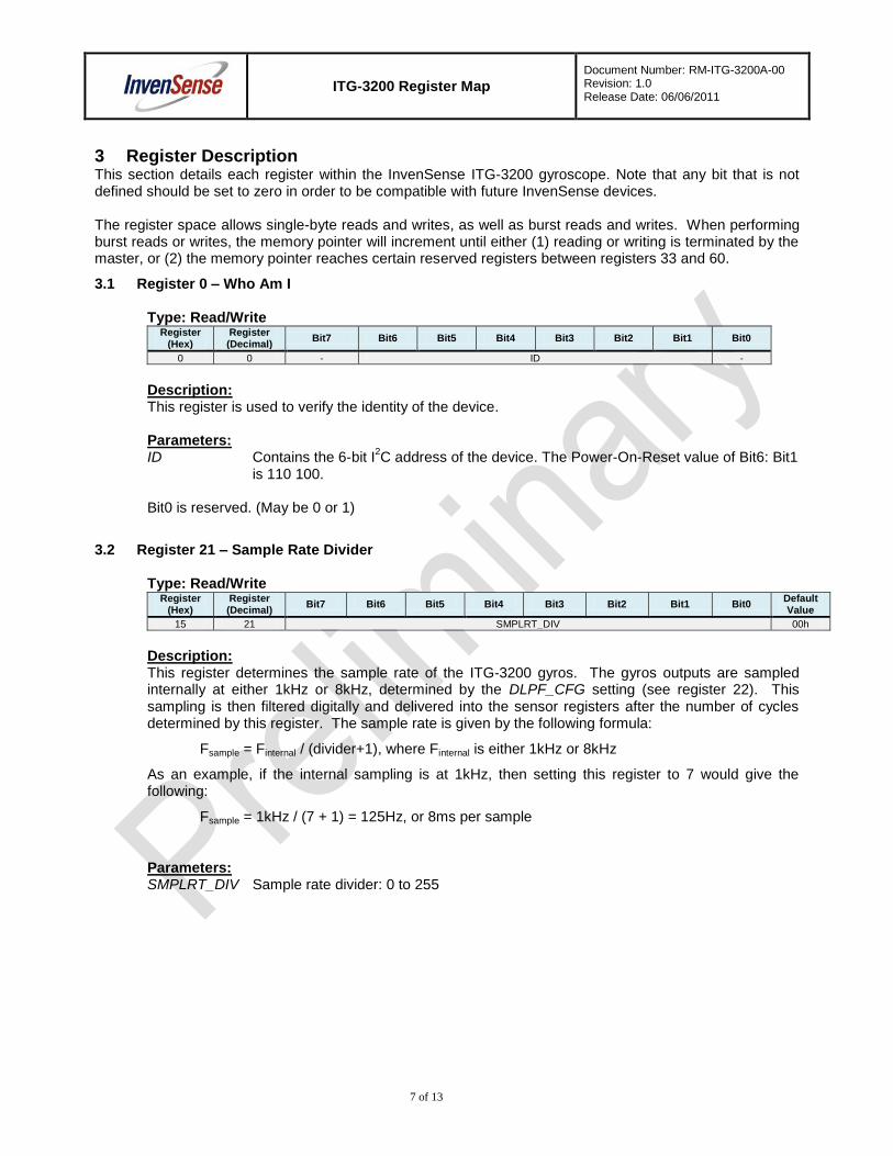
3 Register Description This section details each register within the InvenSense ITG-3200 gyroscope. Note that any bit that is not defined should be set to zero in order to be compatible with future InvenSense devices. The register space allows single-byte reads and writes, as well as burst reads and writes. When performing burst reads or writes, the memory pointer will increment until either (1) reading or writing is terminated by the master, or (2) the memory pointer reaches certain reserved registers between registers 33 and 60.
3.1 Register 0 – Who Am I Type: Read/Write
Register (Hex)
Register (Decimal)
Bit7 Bit6 Bit5 Bit4 Bit3 Bit2 Bit1 Bit0
0 0 - ID -
Description: This register is used to verify the identity of the device. Parameters: ID Contains the 6-bit I
2C address of the device. The Power-On-Reset value of Bit6: Bit1
is 110 100.
Bit0 is reserved. (May be 0 or 1)
3.2 Register 21 – Sample Rate Divider Type: Read/Write
Register (Hex)
Register (Decimal)
Bit7 Bit6 Bit5 Bit4 Bit3 Bit2 Bit1 Bit0 Default Value
15 21 SMPLRT_DIV 00h
Description: This register determines the sample rate of the ITG-3200 gyros. The gyros outputs are sampled internally at either 1kHz or 8kHz, determined by the DLPF_CFG setting (see register 22). This sampling is then filtered digitally and delivered into the sensor registers after the number of cycles determined by this register. The sample rate is given by the following formula:
Fsample = Finternal / (divider+1), where Finternal is either 1kHz or 8kHz
As an example, if the internal sampling is at 1kHz, then setting this register to 7 would give the following:
Fsample = 1kHz / (7 + 1) = 125Hz, or 8ms per sample
Parameters: SMPLRT_DIV Sample rate divider: 0 to 255
ITG-3200 Register Map
Document Number: RM-ITG-3200A-00 Revision: 1.0 Release Date: 06/06/2011
8 of 13
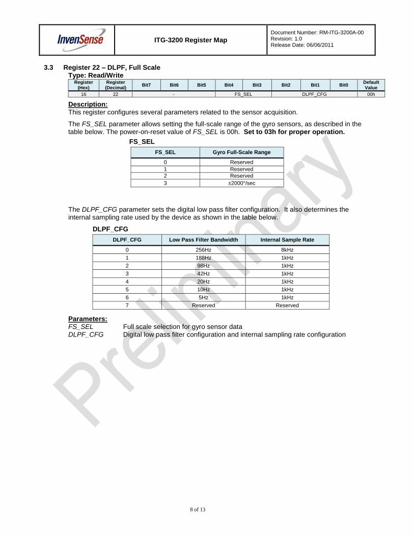
3.3 Register 22 – DLPF, Full Scale
Type: Read/Write Register
(Hex) Register (Decimal)
Bit7 Bit6 Bit5 Bit4 Bit3 Bit2 Bit1 Bit0 Default Value
16 22 - FS_SEL DLPF_CFG 00h
Description: This register configures several parameters related to the sensor acquisition.
The FS_SEL parameter allows setting the full-scale range of the gyro sensors, as described in the table below. The power-on-reset value of FS_SEL is 00h. Set to 03h for proper operation.
FS_SEL
FS_SEL Gyro Full-Scale Range
0 Reserved
1 Reserved
2 Reserved
3 ±2000°/sec
The DLPF_CFG parameter sets the digital low pass filter configuration. It also determines the internal sampling rate used by the device as shown in the table below.
DLPF_CFG
DLPF_CFG Low Pass Filter Bandwidth Internal Sample Rate
0 256Hz 8kHz
1 188Hz 1kHz
2 98Hz 1kHz
3 42Hz 1kHz
4 20Hz 1kHz
5 10Hz 1kHz
6 5Hz 1kHz
7 Reserved Reserved
Parameters: FS_SEL Full scale selection for gyro sensor data DLPF_CFG Digital low pass filter configuration and internal sampling rate configuration

ITG-3200 Register Map
Document Number: RM-ITG-3200A-00 Revision: 1.0 Release Date: 06/06/2011
9 of 13
DLPF Characteristics: The gain and phase responses of the digital low pass filter settings (DLPF_CFG) are shown below:
Gain and Phase vs. Digital Filter Setting
Gain and Phase vs. Digital Filter Setting, Showing Passband Details
-50
-40
-30
-20
-10
0
Magnitu
de (
dB
)
100
101
102
103
-90
-45
0
Phase (
deg)
Bode Diagram
Frequency (Hz)
6 5 4 3 2 1 0
6 5 4 3 2 1 0
-6
-4
-2
0
2
Magnitu
de (
dB
)
100
101
102
103
-15
-10
-5
0
Phase (
deg)
Bode Diagram
Frequency (Hz)
6 5 4 3 2 1 0
6 5 4 3 2 1 0
ITG-3200 Register Map
Document Number: RM-ITG-3200A-00 Revision: 1.0 Release Date: 06/06/2011
10 of 13
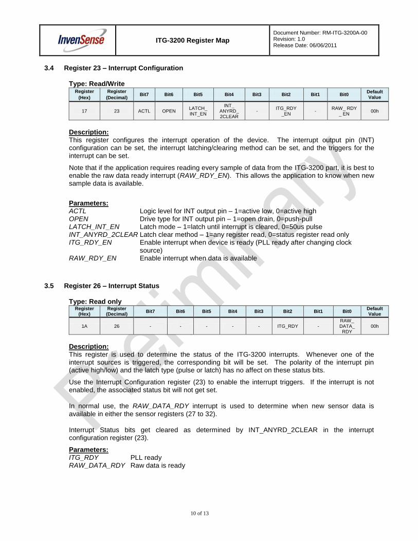
3.4 Register 23 – Interrupt Configuration Type: Read/Write
Register
(Hex)
Register
(Decimal) Bit7 Bit6 Bit5 Bit4 Bit3 Bit2 Bit1 Bit0
Default Value
17 23 ACTL OPEN LATCH_ INT_EN
INT_ ANYRD_ 2CLEAR
- ITG_RDY
_EN -
RAW_ RDY _ EN
00h
Description: This register configures the interrupt operation of the device. The interrupt output pin (INT) configuration can be set, the interrupt latching/clearing method can be set, and the triggers for the interrupt can be set.
Note that if the application requires reading every sample of data from the ITG-3200 part, it is best to enable the raw data ready interrupt (RAW_RDY_EN). This allows the application to know when new sample data is available.
Parameters: ACTL Logic level for INT output pin – 1=active low, 0=active high OPEN Drive type for INT output pin – 1=open drain, 0=push-pull LATCH_INT_EN Latch mode – 1=latch until interrupt is cleared, 0=50us pulse INT_ANYRD_2CLEAR Latch clear method – 1=any register read, 0=status register read only ITG_RDY_EN Enable interrupt when device is ready (PLL ready after changing clock
source) RAW_RDY_EN Enable interrupt when data is available
3.5 Register 26 – Interrupt Status Type: Read only
Register (Hex)
Register (Decimal)
Bit7 Bit6 Bit5 Bit4 Bit3 Bit2 Bit1 Bit0 Default Value
1A 26 - - - - - ITG_RDY - RAW_ DATA_
RDY 00h
Description: This register is used to determine the status of the ITG-3200 interrupts. Whenever one of the interrupt sources is triggered, the corresponding bit will be set. The polarity of the interrupt pin (active high/low) and the latch type (pulse or latch) has no affect on these status bits.
Use the Interrupt Configuration register (23) to enable the interrupt triggers. If the interrupt is not enabled, the associated status bit will not get set.
In normal use, the RAW_DATA_RDY interrupt is used to determine when new sensor data is available in either the sensor registers (27 to 32).
Interrupt Status bits get cleared as determined by INT_ANYRD_2CLEAR in the interrupt configuration register (23).
Parameters: ITG_RDY PLL ready RAW_DATA_RDY Raw data is ready

ITG-3200 Register Map
Document Number: RM-ITG-3200A-00 Revision: 1.0 Release Date: 06/06/2011
11 of 13
3.6 Registers 27 to 34 – Sensor Registers Type: Read only
Register
(Hex)
Register
(Decimal) Bit7 Bit6 Bit5 Bit4 Bit3 Bit2 Bit1 Bit0
1B 27 TEMP_OUT_H
1C 28 TEMP_OUT_L
1D 29 GYRO_XOUT_H
1E 30 GYRO_XOUT_L
1F 31 GYRO_YOUT_H
20 32 GYRO_YOUT_L
21 33 GYRO_ZOUT_H
22 34 GYRO_ZOUT_L
Description: These registers contain the gyro and temperature sensor data for the ITG-3200 parts. At any time, these values can be read from the device; however it is best to use the interrupt function to determine when new data is available.
Parameters: TEMP_OUT_H/L 16-bit temperature data (2’s complement format) GYRO_XOUT_H/L 16-bit X gyro output data (2’s complement format) GYRO_YOUT_H/L 16-bit Y gyro output data (2’s complement format) GYRO_ZOUT_H/L 16-bit Y gyro output data (2’s complement format)
3.7 Register 62 – Power Management Type: Read/Write
Register (Hex)
Register (Decimal)
Bit7 Bit6 Bit5 Bit4 Bit3 Bit2 Bit1 Bit0 Default Value
3E 62 H_RESET SLEEP STBY _XG
STBY _YG
STBY _ZG
CLK_SEL 00h
Description: This register is used to manage the power control, select the clock source, and to issue a master reset to the device.
Setting the SLEEP bit in the register puts the device into very low power sleep mode. In this mode, only the serial interface and internal registers remain active, allowing for a very low standby current. Clearing this bit puts the device back into normal mode. To save power, the individual standby selections for each of the gyros should be used if any gyro axis is not used by the application.
The CLK_SEL setting determines the device clock source as follows:
CLK_SEL
CLK_SEL Clock Source
0 Internal oscillator
1 PLL with X Gyro reference
2 PLL with Y Gyro reference
3 PLL with Z Gyro reference
4 PLL with external 32.768kHz reference
5 PLL with external 19.2MHz reference
6 Reserved
7 Reserved
On power up, the ITG-3200 defaults to the internal oscillator. It is highly recommended that the device is configured to use one of the gyros (or an external clock) as the clock reference, due to the improved stability.

ITG-3200 Register Map
Document Number: RM-ITG-3200A-00 Revision: 1.0 Release Date: 06/06/2011
12 of 13
Parameters: H_RESET Reset device and internal registers to the power-up-default settings SLEEP Enable low power sleep mode STBY_XG Put gyro X in standby mode (1=standby, 0=normal) STBY_YG Put gyro Y in standby mode (1=standby, 0=normal) STBY_ZG Put gyro Z in standby mode (1=standby, 0=normal) CLK_SEL Select device clock source

ITG-3200 Register Map
Document Number: RM-ITG-3200A-00 Revision: 1.0 Release Date: 06/06/2011
13 of 13
This information furnished by InvenSense is believed to be accurate and reliable. However, no responsibility is assumed by InvenSense for its use, or for any infringements of patents or other rights of third parties that may result from its use. Specifications are subject to change without notice. InvenSense reserves the right to make changes to this product, including its circuits and software, in order to improve its design and/or performance, without prior notice. InvenSense makes no warranties, neither expressed nor implied, regarding the information and specifications contained in this document. InvenSense assumes no responsibility for any claims or damages arising from information contained in this document, or from the use of products and services detailed therein. This includes, but is not limited to, claims or damages based on the infringement of patents, copyrights, mask work and/or other intellectual property rights. Certain intellectual property owned by InvenSense and described in this document is patent protected. No license is granted by implication or otherwise under any patent or patent rights of InvenSense. This publication supersedes and replaces all information previously supplied. Trademarks that are registered trademarks are the property of their respective companies. InvenSense sensors should not be used or sold in the development, storage, production or utilization of any conventional or mass-destructive weapons or for any other weapons or life threatening applications, as well as in any other life critical applications such as medical equipment, transportation, aerospace and nuclear instruments, undersea equipment, power plant equipment, disaster prevention and crime prevention equipment.
InvenSense® is a registered trademark of InvenSense, Inc. ITG™, ITG-3200™, MotionApps™, MPU™, MotionProcessing Unit™, MotionProcessor™, MotionProcessing™, MotionFusion™, MPU-3050™, MPU-6050™, IMU-3000™ are trademarks of InvenSense, Inc.
©2011 InvenSense, Inc. All rights reserved.


