
• 2001 IEEE International Solid-State Circuits Conference 0-7803-6608-5 ©2001 IEEE
ISSCC 2001 / SESSION 23 / ANALOG TECHNIQUES / 23.2
23.2 Dynamically Biased 1MHz Low-pass Filter with 61dB Peak SNR and 112dB Input Range
Nagendra Krishnapura, Yannis Tsividis
Columbia University, New York, NY
In conventional analog filters operated in class-A mode, bias cur-rents are large enough to accommodate the largest expected peakinput signal. When only a small input signal (including in-bandand out-of-band components) is present, these large bias currentsunnecessarily waste power and create noise. A more optimal situ-ation results if bias currents can be dynamically set by the system,depending on the peak value of the total signal being applied oranticipated at the input. However, dynamically varying the biascurrents in a filter normally causes unacceptable disturbances atits output. This filter has bias currents that can be varied over sev-eral orders of magnitude—for optimum power consumption andnoise at each total input signal level—without disturbing the out-put. Although the filter is internally nonlinear and time-varying, itis externally linear and time-invariant [1].
The chip uses the first-order log-domain filter [2] shown inFigure 23.2.1a as its building block for reasons that will be appar-ent below. Desired currents are forced into the collectors of thetransistors Q1p and Q3p using feedback-controlled current sourcesIfb. The log-domain filter is linear and time-invariant between thelarge signal currents i1p and i4p in its input and output transis-tors (assuming i1p>0). The time-domain and frequency-domainrelationships between i1p and i4p are given in Figure 23.2.1c. Thecurrents I2,3 and the capacitor C1 determine the dc gain k and thepole ωp of the filter. The total input current i1p is the sum of a sig-nal current iin and a dc bias Ibias. With iin=0, the integrated out-put noise in,4p (due to collector shot noise of Q1p–4p) is given bythe expression in Figure 23.2.1c. The input bias Ibias affects theoutput noise but not the transfer function. Ibias can be varied inaccordance with the envelope of the input so that it is slightly larg-er than the minimum required value for i1p to stay positive at alltimes [3]. Such dynamic biasing lowers the power consumption andthe output noise of the filter for small inputs and, at the otherextreme, can accommodate large inputs. However, a time varyingIbias(t) results in transients in the current i4p of the output tran-sistor Q4p. To overcome this problem, the single-ended filter shownin Figure 23.2.1a is duplicated and operated with the same biasIbias but an opposite input signal –iin as shown in Figure 23.2.1b[4]. Because of the large signal linearity of the log-domain filtersthe component due to Ibias(t) in the two halves of the filter is thesame and cancels in the differential output iout=i4p–i4n. The rela-tion between iin and iout is linear and time-invariant. At the sametime, the use of dynamic biasing accomplishes internal “compand-ing” (compressing/expanding)[1]. A reduction of Ibias inFigure 23.2.1 increases the gain (current to voltage) from the inputsignal iin to the internal voltages - e.g., vel, the emitter voltage ofQ1p due to the reduction of the latter’s transconductance - of thefilter [3, 4] and thus helps maintain an adequate S/N.
A 3rd-order Butterworth filter (based on the RLC ladder inFigure 23.2.2a) with a -3dB bandwidth of 1MHz is fabricated to eval-uate the dynamic biasing technique. The RLC prototype is redrawnas an interconnection of 1st-order stages in Figure 23.2.2b. The gainof 2 at the input cancels the 6 dB attenuation of the ladder filter.Figure 23.2.2c shows a simplified picture of the 3rd-order pseudo-differential log-domain filter. Each half of the filter consists of a 3rd-order filter core with logarithmic compression (Q1p) and exponentialexpansion (Q4p) blocks. The 3rd-order filter core has three stages,each of which is similar to the 1st-order filter core - Q2p,3p,I2,3 andC1 - in Figure 23.2.1a.
The dominant source of distortion is the finite output resistance ofthe bipolar transistors and the current sources. The collector volt-
age swings of Q1p (and other transistors in the core) are minimizedby using a large transconductance in the feedback path around thetransistors. A bipolar transistor Qf driven by a source follower(Figure 23.2.2d) realizes such a large transconductance. An MOScapacitor Cc is used to stabilize the loop. Cascode current sourceswith long channel MOS transistors are used in the filter to mini-mize their output conductance and noise. Figure 23.2.3 shows thechip micrograph.
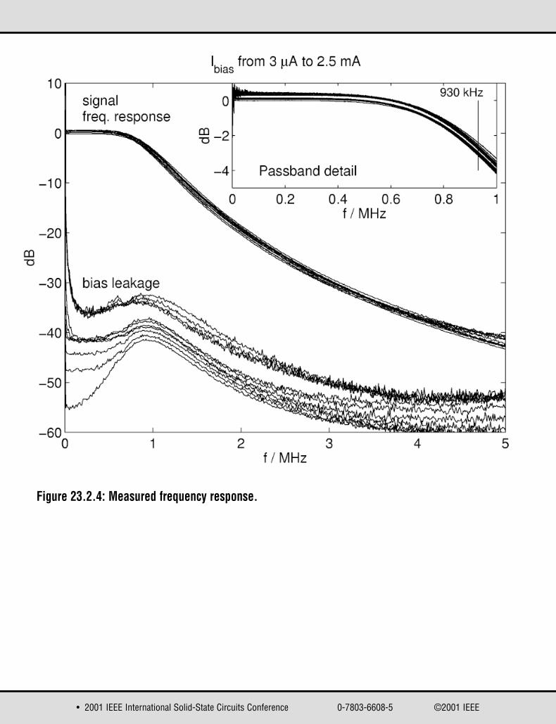
Figure 23.2.4 shows the measured frequency response of the filterfor values of the bias current Ibias (Figure 23.2.2c) in the range3µA to 2.5mA. The measured bandwidth is close to 930kHz for allbias currents. There is a small variation in the passband gainwhen the bias is varied. Although the cutoff frequency and the dcgain of the filter can be tuned (Figure 23.2.1c), there was no needto do so for the measurements presented here. The residual “leak-age” of Ibias to the differential output due to mismatch is alsoshown in Figure 23.2.4.
For the following measurements, the bias current Ibias is set totwice the amplitude of the single-ended input iin in Figure 23.2.2c,unless that value was less than 3µA, in which case Ibias was main-tained at 3µA. With such a dynamic biasing arrangement, themeasured rms values of the signal and the noise in the differentialoutput are plotted in Figure 23.2.5a vs. the differential inputpeak. Decreasing Ibias decreases the noise, down to 4.4nA rms,corresponding to the smallest Ibias of 3µA. Figure 23.2.5b showsmeasured output signal to noise ratio (S/N), signal to total har-monic distortion ratio (S/D), and signal to 3rd-order intermodula-tion ratio (S/IM3, measured with two tones at 980kHz and 1020kHz) as a function of the differential peak input.
Figure 23.2.6a shows the response of the filter to a 600kHz sinu-soid with a differential peak value of 40µA when the bias Ibias isswitched from 24µA (which is 20% larger than the single-endedpeak input) to 114µA. As seen, the output is practically unaffectedby transients in Ibias. The results in Figs. 23.2.4 and 23.2.6a pointto the external time-invariance of the filter in presence of a vary-ing Ibias. Figure 23.2.6b shows the current and power consump-tion of the filter as a function of the differential peak input.
The filter maintains S/N>0 dB and THD < –41dB for total inputvalues ranging over 112dB (Figure 23.2.5b). The filter is not equiv-alent to a conventional filter with 112dB dynamic range, as the lat-ter would have S/N = 112dB with the largest input. However, itwould require orders of magnitude greater power dissipation toachieve this [5].
This dynamically-biased filter is suitable for cases where a modestand a near-optimum power dissipation must be maintained over alarge range of input amplitudes. Figure 23.2.7 summarizes mea-sured performance. The chip presented here represents over anorder of magnitude improvement in power efficiency compared topreviously-published filters.
Acknowledgments: The authors thank Lucent Technologies for chip fabrication. This work was sup-ported by the National Science Foundation under Grant no. CCR-99-02781.
References:[1] Y. Tsividis, “Externally Linear Time-Invariant Systems and theirApplications to Companding Signal Processors”, IEEE TCAS-II, vol. 44, no. 2,pp. 65-85, Feb. 1997. [2] M. Punzenberger et al., “A 1.2-V Low Power BiCMOS Class AB Log-DomainFilter”, IEEE JSSC, vol. 32, pp. 1968-1978, Dec. 1997. [3] D. R. Frey et al., “Syllabically Companding Log Domain Filter usingDynamic Biasing”, Electron. Lett., vol. 33, no. 18, pp. 1506-1507, 28 Aug. 1997. [4] N. Krishnapura et al., “Simplified Technique for Syllabic Companding inLog-domain Filters”, Electron. Lett., vol. 36, no. 15, pp. 1257-1259, 20th Jul.2000. [5] E. Vittoz, “Low power low-voltage limitations and prospects in analogdesign”, in R. J. v. d. Plassche et al., eds., Analog Circuit Design, Low-Power,Low-Voltage, Integrated Filters and Smart-Power, Boston: Kluwer, 1995.

• 2001 IEEE International Solid-State Circuits Conference 0-7803-6608-5 ©2001 IEEE
Figure 23.2.6: (a) Differential o/p with a time-varying Ibias, (b) power consumption.Figure 23.2.5: Measured signal, noise, and distortion.
Figure 23.2.1: (a) 1st order log-domain filter, (b) replica, (c) governing equations.Figure 23.2.2: (a) RLC prototype, (b) block diagram, (c) log-domain realization, (d) feedback circuitry.
Figure 23.2.3: Chip micrograph. Figure 23.2.4: Measured frequency response.
ISSCC 2001 / February 7, 2001 / Salon 7 / 2:00 PM

Figure 23.2.7: Performance summary and comparison.
• 2001 IEEE International Solid-State Circuits Conference 0-7803-6608-5 ©2001 IEEE

• 2001 IEEE International Solid-State Circuits Conference 0-7803-6608-5 ©2001 IEEE
Figure 23.2.1: (a) 1st order log-domain filter, (b) replica, (c) governing equations.

• 2001 IEEE International Solid-State Circuits Conference 0-7803-6608-5 ©2001 IEEE
Figure 23.2.2: (a) RLC prototype, (b) block diagram, (c) log-domain realization, (d) feedback circuitry.

• 2001 IEEE International Solid-State Circuits Conference 0-7803-6608-5 ©2001 IEEE
Figure 23.2.3: Chip micrograph.
• 2001 IEEE International Solid-State Circuits Conference 0-7803-6608-5 ©2001 IEEE
Figure 23.2.4: Measured frequency response.

• 2001 IEEE International Solid-State Circuits Conference 0-7803-6608-5 ©2001 IEEE
Figure 23.2.5: Measured signal, noise, and distortion.

• 2001 IEEE International Solid-State Circuits Conference 0-7803-6608-5 ©2001 IEEE
Figure 23.2.6: (a) Differential o/p with a time-varying Ibias, (b) power consumption.

• 2001 IEEE International Solid-State Circuits Conference 0-7803-6608-5 ©2001 IEEE
Figure 23.2.7: Performance summary and comparison.


