
Introduction to PCB Design 1
AED703Printed Circuit Board Design - 1
•Instructors:
– J. Ebden
– J. Kawenka

Introduction to PCB Design 2
What is a PCB?
• Definition:
Printed Circuit – an electric circuit in which the conducting paths connecting circuit components are affixed to a flat insulating base board*
*Columbia Encyclopedia, 6th ed, 2001
Introduction to PCB Design 3
What is a PCB?
• PWB vs PCB
PWB – copper traces and pads create point-to-point connection of components.
PCB – a PWB that contains components that are embedded in the copper.

Introduction to PCB Design 4
Growth of the PWB Industry
• In the Beginning• Advances Made• Today• Design Technology Growth

Introduction to PCB Design 5
In the Beginning
• Engineer– Concept of Design– Rough “scribble” of concept– Breadboard proofing of concept

Introduction to PCB Design 6
In the Beginning
• Designer– Hand draw full schematic– Hand draw layout of component placement
(2X, 4X)– Hand inking of components and board
nomenclature– Drill templates created using dots, donuts,
and symbols

Introduction to PCB Design 7
In the Beginning
• Manufacturer– Photo-reduction of taped artwork– Chemical etching of copper laminates– Hand cut silk screens to squeegee on to
board– “Bullseye” drilling of holes– Hand mounting and soldering of
components– Hand probes used to test functionality

Introduction to PCB Design 8
Advances Made
• Manufacturing– First to utilize advances in automation and
computers– Digitizing replaces photo-reduction– NC Drill replaced “bullseye” drilling– Photographic imaging to create silk screens– “Pick & Place” machines for component
mounting– Wave soldering machines reduce hand
soldering

Introduction to PCB Design 9
Advances Made
• Designing– Hand drawing layouts digitized to create 1X
film artwork– CAD programs developed for board layout– Output of Gerber data to create 1X film
artwork– Output of NC drill tapes

Introduction to PCB Design 10
Today
• Engineer
– Develop concept and schematic in CAD/CAE tools
– Simulating design replaces hand calculations

Introduction to PCB Design 11
Today
• Designer– CAD tools tie schematic and layout for
“intelligent” designs– Component placement and circuit routing
automated– Data output increased to include: Gerber
data, NC drill data, component placement data, net list data, testing data, etc

Introduction to PCB Design 12
Today
• Manufacturer– Use Gerber and NC drill data to fabricate
bare board– Use component placement data to assemble
board– Use net list and testing data to verify final
product
Introduction to PCB Design 13
Design Technology Growth
• Smaller product packaging– More functionality per circuit card– Smaller components, surface mount and
micro-technology
• Demand for faster time to market– Panelization for easier handling– Increased automation for faster turn around
• Increased demand for QC

Introduction to PCB Design 14
Industry standards
• Board Level
– IPC-4101 Specification for base materials– IPC-L-125 Materials for high speed/high
frequency boards– IPC-2221 Generic standard for printed
board design– IPC-SM-782 Surface mount design and land
pattern– IPC-SM-840 Solder mask standard– IPC-TM-650 Test methods manual
Introduction to PCB Design 15
Industry standards
• Assembly Level
– IPC-A-610 Acceptability of printed board assemblies
– J-STD-001 Requirements for soldered electrical and
electronic assemblies

Introduction to PCB Design 16
Industry standards
• Documentation
• MIL-STD-100 Engineering Drawing Practices
• ANSI Y14.100 Replaces MIL-STD-100 for non-military
• IPC-D-325 Documentation requirements for printed boards, assemblies, and support drawings
• ASME Y14.5Dimensioning and Tolerancing

Introduction to PCB Design 17
Classes and types
• Performance classes– Determined by end use of product
• Board types– Bare board configurations
• Producibility levels– Circuit design complexity
• Assembly classes– Component mounting complexity
Introduction to PCB Design 18
Performance Classes for Electronics Products
• Class 1 – General
– Some computers and computer peripherals– Main importance is functionality. Cosmetic
imperfections not important

Introduction to PCB Design 19
Performance Classes for Electronics Products
• Class 2 – Dedicated Service
– Communications, sophisticated business machines, instruments
– Extended life and uninterrupted service desired, but not required

Introduction to PCB Design 20
Performance Classes for Electronics Products
• Class 3 – High reliability
– Life support systems, critical weapons systems
– Continued performance or performance on demand is required
– Downtime is not acceptable

Introduction to PCB Design 21
Board Types
• Type 1 - Single sided printed board• Type 2 - Double sided printed board• Type 3 - Multilayer without blind and/or buried
vias• Type 4 - Multilayer with blind and/or buried
vias• Type 5 - Multilayer metal core without blind
and/or buried vias• Type 6 - Multilayer metal core with blind
and/or buried vias

Introduction to PCB Design 22
Type 1 Board

Introduction to PCB Design 23
Type 2 Board
Introduction to PCB Design 24
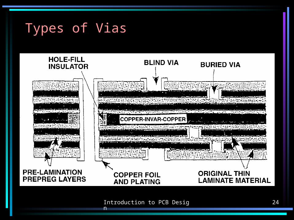
Types of Vias

Introduction to PCB Design 25
Producibility Levels
• Level A - General Design Complexity
(preferred)• Level B - Moderate Design Complexity (Standard)• Level C - High Design Complexity (Reduced Producibilty)
Introduction to PCB Design 26
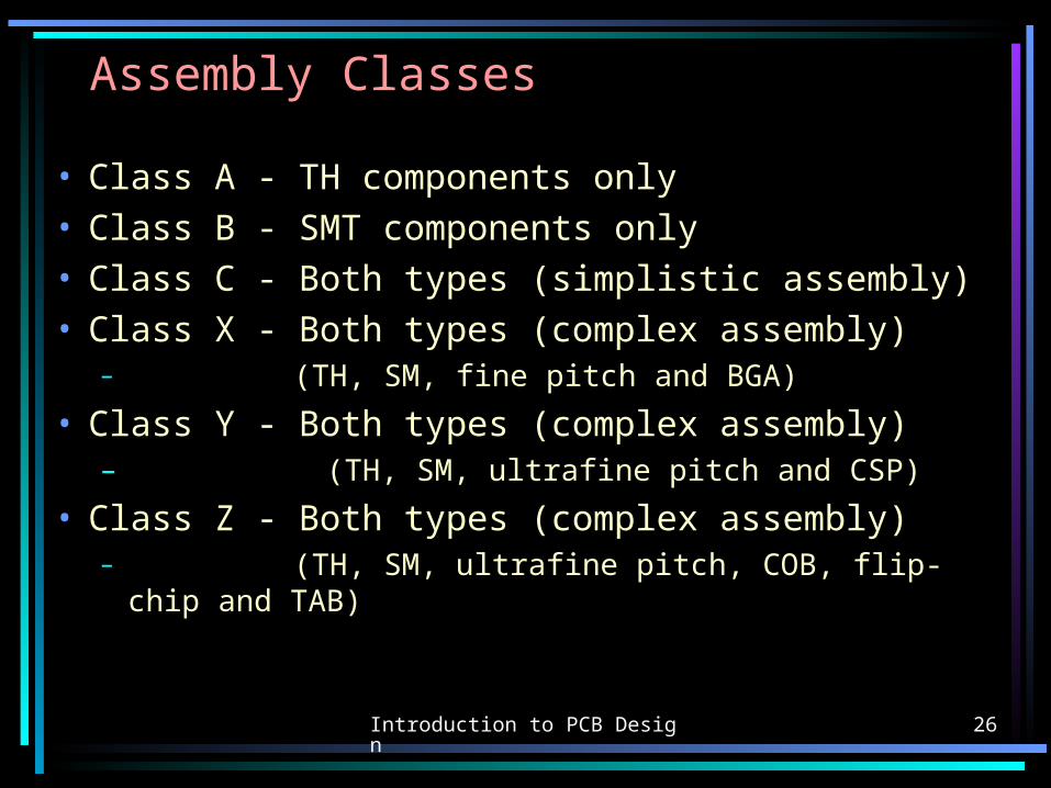
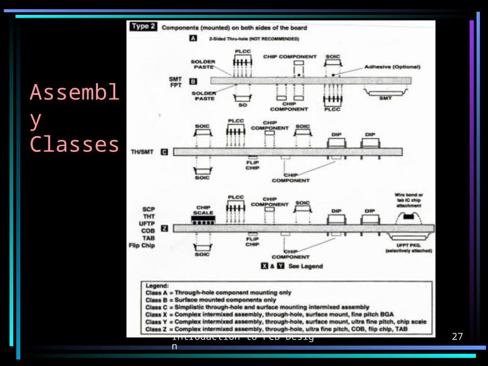
Assembly Classes
• Class A - TH components only• Class B - SMT components only• Class C - Both types (simplistic assembly)• Class X - Both types (complex assembly)
– (TH, SM, fine pitch and BGA)
• Class Y - Both types (complex assembly)– (TH, SM, ultrafine pitch and CSP)
• Class Z - Both types (complex assembly)– (TH, SM, ultrafine pitch, COB, flip-chip and TAB)
Introduction to PCB Design 27
Assembly Classes

Introduction to PCB Design 28
Components• Types of Components
– Passive vs Active– Symbols and Designations
• Package Types– Through-hole (TH)– Surface Mount (SM)
• Surface Mount Lead Styles• Polarity and Orientation

Introduction to PCB Design 29
Types of Components
Passive Components - Basic function of component does not change when they receive a signal
Component Function Symbol Designation
Capacitor Stores anddischargeselectricity
C
Resistor Limits the flow ofelectrical current R
Inductor Creates magneticfield whencurrent flowsthrough
L
+

Introduction to PCB Design 30
Types of Components
Active Components - Basic function does change when they receive a signal
C o m p o n e n t F u n c t i o n S y m b o l D e s i g n a t i o n
D io d e O n ly a l l o w s c u r r e n t t ofl o w in o n e d i r e c t i o n .C h a n g e s A C t o D C .V o l t a g e l im i t e r f o r D C( Z e n e r ) . S p e c ia l i t y d io d e s
D o r C R
T r a n s i s t o r L im i t s t h e fl o w o fe le c t r i c a l c u r r e n t Q
I n t e g r a t e dC i r c u i t ( I C )
V a r io u s s i g n a l p r o c e s s in gf u n c t io n s
D e t e r m in e d b yf u n c t io n o fd e v i c e
U
PNPNP N

Introduction to PCB Design 31
Package Types
PackageType
Description TypicalComponents
Axial Lead Two leads extending from eachside of the component
Resistors, Capacitors,Diodes, Inductors
Radial Lead Two or more leads extendingfrom side of the component
Capacitors, Diodes,Transistors, Crystals,some ICs
SIP Single Inline PackageA row of leads in a single straightline
Resistor Networks,Capacitor Networks,Diode Arrays
DIP Dual Inline PackageTwo rows of pins in a parallelstraight line
ICs, Sockets, ResistorNetworks, CapacitorNetworks, Diode Arrays
PGA Pin Grid ArrayMultiple pins extending frombottom of component in a gridpattern
ICs, Sockets
Through-Hole - Components with leads that are inserted through mounting holes in the circuit board

Introduction to PCB Design 32
Package Types
PackageType
Description TypicalComponents
Chip Usually ceramic bodied package with metaltermination on each end - rectangular
Resistors,Capacitors,Inductors, Diodes
MELF Metal Electrode FaceMetal terminations on each end ofcylindrical body
Resistors, Diodes
LCC Leadless Chip CarrierNo leads, metallization in form ofcastellations for attachment
ICs
SOIC Small Outline Integrated CircuitSimilar to DIP package with leads formedfor surface mounting
ICs
QFP Quad Flat PackLeads extend from four sides of component
ICs
BGA Ball Grid ArraySurface mount version of PGA. Leads aretiny metal balls on bottom of component
ICs
Surface Mount - Components with leads that are mounted directly onto lands on the surface of the
board

Introduction to PCB Design 33
Surface Mount Lead Styles
• Gull Wing
• J-Lead
• L-Lead
• Flat Lead
• Ball
• Lead Pitch - Distance from centre of one pin to centre of adjacent pin
– Standard: 20 - 100 mils– Fine: 12 - 20 mils– Ultrafine: <12 mils

Introduction to PCB Design 34
Passive Components
Resistor Tantalum Capacitor

Introduction to PCB Design 35
Passive Components
Ceramic Capacitor

Introduction to PCB Design 36
Active Components
Small outline transistor (SOT)

Introduction to PCB Design 37
Through Hole Packages
DIP-24 DIP-14 (7400)

Introduction to PCB Design 38
Through Hole Packages
PGA
Introduction to PCB Design 39
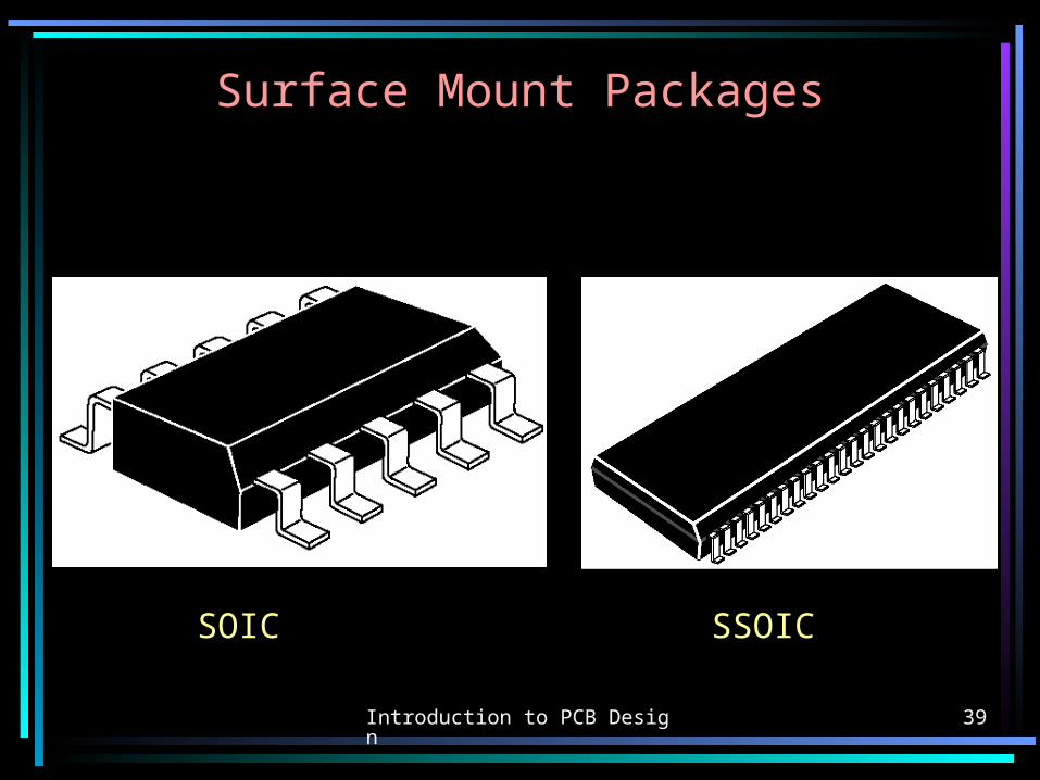
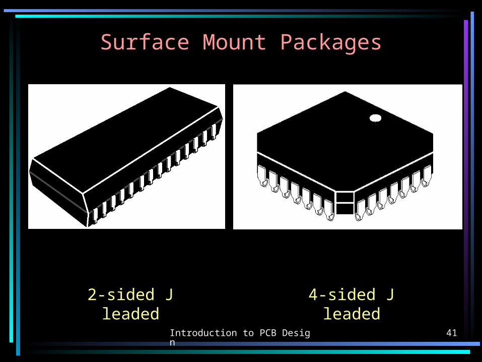
Surface Mount Packages
SOIC SSOIC

Introduction to PCB Design 40
Surface Mount Packages
QFP PQFP
Introduction to PCB Design 41
Surface Mount Packages
2-sided J leaded 4-sided J leaded

Introduction to PCB Design 42

Introduction to PCB Design 43
Polarity and Orientation
• Polarity - Positive and negative ends of a two pin device
– Positive or anode lead graphical representation
• Capacitor - Identified with a (+) and/or square pad• Diode - Identified flat end of triangle and/or square pad
– Negative or cathode lead graphical representation
• Capacitor - Not defined• Diode - Identified by bar end of diode symbol

Introduction to PCB Design 44
Polarity and Orientation
• Orientation - Identification of pin 1 of multi-pin devices
– Dot, notch or number identification on component
– Square pad or silkscreen dot on board surface
– Pin count direction typically counter-clockwise from pin 1
Introduction to PCB Design 45
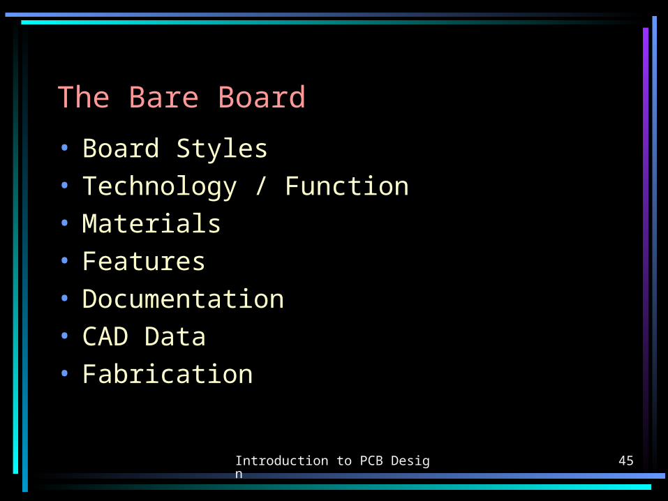
The Bare Board
• Board Styles• Technology / Function• Materials• Features• Documentation• CAD Data• Fabrication

Introduction to PCB Design 46
Board Styles
• Rigid– Most common board style– Solid construction, hard mounted into next assembly
• Rigid-Flex– Sectional, multiple rigid boards inter-connected with
flexible circuits
• Flex– Flexible circuits, typically used to replace cabling within
a system
• Hybrid– Very small circuits, generally encapsulated and mounted
onto larger boards

Introduction to PCB Design 47
Technology / Function• Analog
– Typical functions are op-amps, voltage converters, power supplies
• Digital– Typical function is signal processing
• RF– Function to produce radio frequencies, usually in the
super high frequency range
• Frequency Ranges:
Low Frequency (LF) = 100 kHz
Medium Frequency (MF) = 300-3000kHz
High Frequency (HF) = 3-30 Mhz
Very High Frequency (VHF) = 30-300 MHz
Ultra High Frequency (UHF) = 300-3000 MHz
Super High Frequency (SHF) = 3-30 GHz

Introduction to PCB Design 48
Materials
• FR4– Woven glass reinforcement with epoxy resin binder– FR indicates it meets UL requirements for flame retardance
• PTFE– Polytetrafluoroethylene (Teflon)
• RO4350– Woven glass reinforcement with ceramic filled thermoset
• Polyimide Film– Polyimide resin system without glass reinforcement, used
for flexible film

Introduction to PCB Design 49
Features
• Mechanical Outline– Defines overall area for board design
• Clearances– Board edge, mating area at next assembly
• Mounting Holes– Location, size, hardware used (preference =
grid in multiples of 5 mils)
• Tooling Holes – Used throughout fabrication, assembly, and
testing of boards
Introduction to PCB Design 50
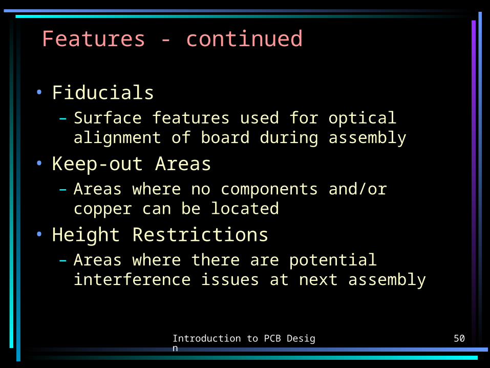
Features - continued
• Fiducials– Surface features used for optical alignment
of board during assembly
• Keep-out Areas– Areas where no components and/or copper
can be located
• Height Restrictions– Areas where there are potential interference
issues at next assembly

Introduction to PCB Design 51
Features - continued
• Fixed Component Location– Connector locations for mating critical
component locations
• Additional Mechanical Hardware– Card guides, stiffeners, sockets

Introduction to PCB Design 52
Features - continued
• Design, fabrication, and manufacturing constraints– Board material– Board thickness / Layer stack-up– Via size– Voltages and currents used for circuits– Critical circuit routing requirements– Thermal considerations– Fabrication and assembly methods

Introduction to PCB Design 53
Documentation - Schematic
Schematic.pdf

Introduction to PCB Design 54
Documentation - Fabrication Drawing
Fabrication Drawing

Introduction to PCB Design 55
Documentation - Assembly Drawing
Introduction to PCB Design 56
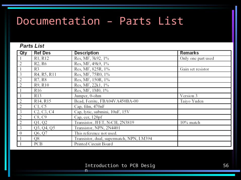
Documentation – Parts List
Introduction to PCB Design 57
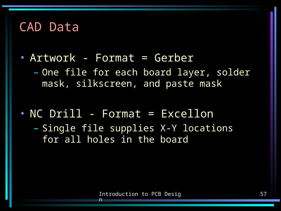
CAD Data
• Artwork - Format = Gerber– One file for each board layer, solder mask,
silkscreen, and paste mask
• NC Drill - Format = Excellon– Single file supplies X-Y locations for all holes
in the board

Introduction to PCB Design 58
CAD Data - continued• Additional files supplied
– IPC-D-350: Printed board description in digital form– Neutral file: Mentor Graphics format, complete
layout data– Geoms file: ASCII description of component
geometries– Nets file: ASCII listing of component pins connect
by net name– Traces file: ASCII listing or each trace on the
board, following each vertex and via
Introduction to PCB Design 59
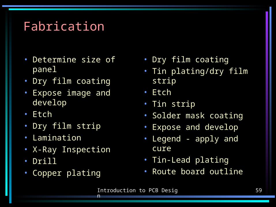
Fabrication
• Determine size of panel• Dry film coating• Expose image and
develop• Etch• Dry film strip• Lamination• X-Ray Inspection• Drill• Copper plating
• Dry film coating• Tin plating/dry film
strip• Etch• Tin strip• Solder mask coating• Expose and develop• Legend - apply and
cure• Tin-Lead plating• Route board outline
Introduction to PCB Design 60
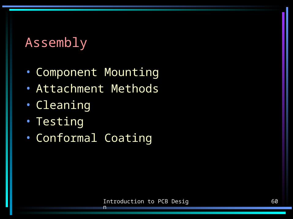
Assembly
• Component Mounting• Attachment Methods• Cleaning• Testing• Conformal Coating

Introduction to PCB Design 61
Assembly - Component Mounting
• Automatic Insertion - TH components
– Board changes position under insertion head
– Dip Inserter - Tube feeds DIPs into insertion head
– Axial and Radial Inserter - components are sequenced and taped, then fed into lead former, then insertion head

Introduction to PCB Design 62
Assembly - Component Mounting (continued)
• Automatic Placement - SM components
– Board remains stationary– Chip Shooter - for mounting chip components– Vacuum Nozzle - selection and placement of larger
components
• Manual Placement
– Unique and odd components formed and mounted by hand
Introduction to PCB Design 63
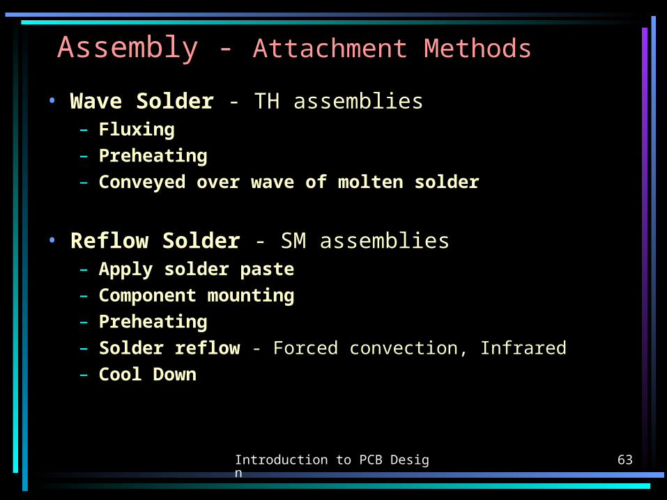
Assembly - Attachment Methods
• Wave Solder - TH assemblies– Fluxing– Preheating– Conveyed over wave of molten solder
• Reflow Solder - SM assemblies– Apply solder paste– Component mounting– Preheating– Solder reflow - Forced convection, Infrared– Cool Down

Introduction to PCB Design 64
Assembly - Attachment Methods (continued)
• Hand Solder– Used for temperature sensitive or odd-
form components
• Vapour Phase Solder
• Laser Solder
• Bar Solder

Introduction to PCB Design 65
Assembly - Cleaning
• Attachment methods leave behind flux residue that can be conductive or corrosive
• Normal handling through assembly process can leave behind contaminants
• Cleaning method dependent on contamination– Sometimes a simple water solution sufficient– Otherwise a more active cleaning agent required
• “No-Clean” soldering– Uses flux that is non-conductive and non-corrosive– Needs investigation for compatibility with other
materials

Introduction to PCB Design 66
Assembly - Testing and Rework
• Initial testing of assembly should be done prior to finalising assembly process. Any rework required per findings in testing is easier to perform
• Possible rework required:– Component replacement– Trace or pad repair– Cuts and jumps
Introduction to PCB Design 67
Assembly - Conformal Coating
• Organic coating for environmental protection– Temperature extremes– Humidity– Corrosive atmosphere– Salt water
• Application methods– Brush– Spray– Dip– Curtain coat– Vacuum deposition

Introduction to PCB Design 68
Assembly - Testing
• Board Level• Assembly• Final Assembly

Introduction to PCB Design 69
Assembly - Testing - Board Level
• Test Coupons (Quality Strip)– Verify fabrication process
• Bare Board Test– Circuit continuity checked at every
termination– Checks for shorts or opens– “Golden Board” test– One or two sided check
• two sided is more expensive• need clam-shell fixture
Introduction to PCB Design 70
Assembly - Testing - Assembly Level
• ICT - (In-Circuit Test)– Used to find shorts, opens, wrong parts,
reversed parts, bad devices and other manufacturing defects
• Functional Test– Verifies functionality of entire board or
group of components
• HAST - (Highly Accelerated Stress Test)– Determines reliability of product under
environmental conditions

Introduction to PCB Design 71
Assembly - Testing - Assembly Level (continued)
• AOI - (Automatic Optical Inspection)– Verifies component position and orientation
• AXI - (Automatic X-Ray Inspection)– Solder joint inspection
Introduction to PCB Design 72
Assembly - Final Assembly
• Functional Test– Verify final assembly performs as specified
(designed)
• Burn- in– Unit turned on and left running for 4-24
hours– Identifies “infant mortality” problems

Introduction to PCB Design 73
Teamwork
• Why is teamwork important?• Tools for Interaction• Results

Introduction to PCB Design 74
Why is teamwork important?
• Questions for the PCB designer so h/she can produce the best design:– Where is product being used?
• Customer requirements, System engineer
– What is the technology of the design?• Customer requirements, Electrical engineer
– What are the geometric parameters of the board?• Mechanical engineer
– Are there special characteristics to be considered?• Mechanical. Electrical, Manufacturing, Test engineers
– How are the boards fabricated,assembled,tested?• Mechanical. Electrical, Manufacturing, Test engineers

Introduction to PCB Design 75
Tools for Interaction
• Concurrent Engineering– Team of multiple functions working together to
develop a single design or product
• Input forms/Checklists– Documented description of need and requirements
• DFM -(Design for Manufacturing)– Communication between designer and
manufacturing
• DFT -(Design for Test)– Communication between designer and test
engineer

Introduction to PCB Design 76
Results
• Ease of manufacturing and testing• Early detection of defects• Quicker time to market• Higher product quality• Increased product reliability• Satisfied customer


