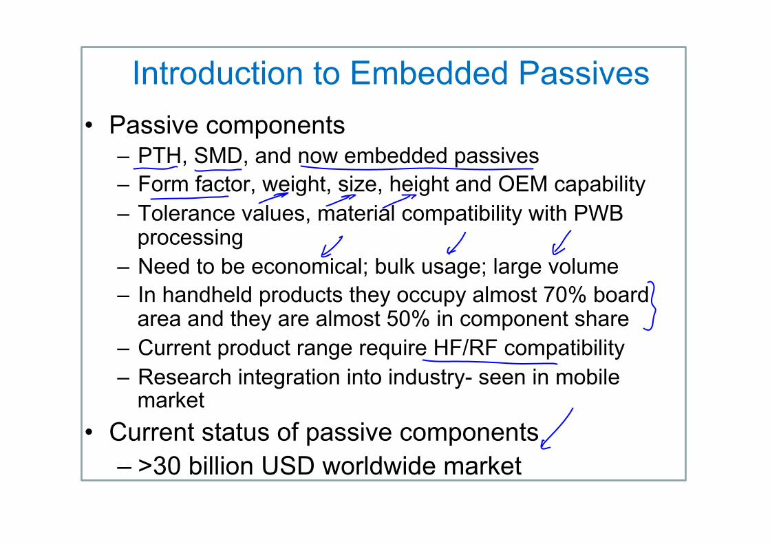
Introduction to Embedded Passives • Passive components
– PTH, SMD, and now embedded passives – Form factor, weight, size, height and OEM capability – Tolerance values, material compatibility with PWB
processing – Need to be economical; bulk usage; large volume – In handheld products they occupy almost 70% board
area and they are almost 50% in component share – Current product range require HF/RF compatibility – Research integration into industry- seen in mobile
market • Current status of passive components
– >30 billion USD worldwide market
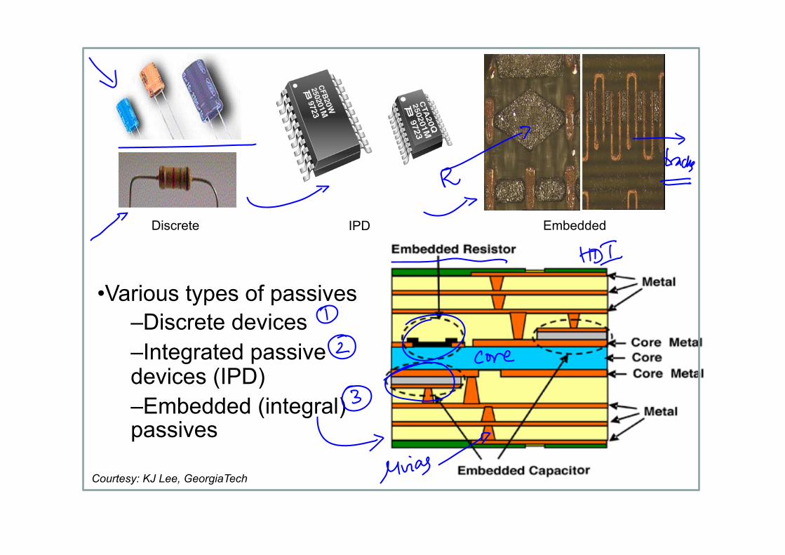
Discrete IPD Embedded
• Various types of passives – Discrete devices – Integrated passive devices (IPD) – Embedded (integral) passives
Courtesy: KJ Lee, GeorgiaTech

Industry impact
Source: Nikkei Publications; Nikkei Electronics Asia; May 2003 issue
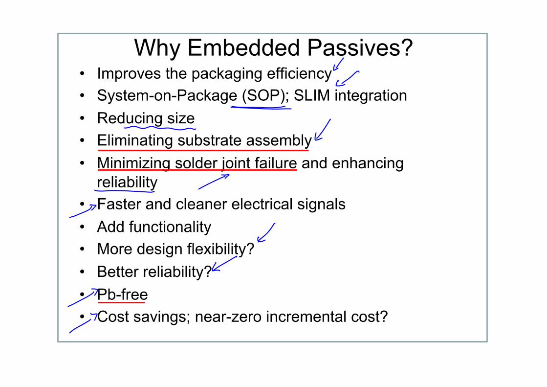
Why Embedded Passives? • Improves the packaging efficiency • System-on-Package (SOP); SLIM integration • Reducing size • Eliminating substrate assembly • Minimizing solder joint failure and enhancing
reliability • Faster and cleaner electrical signals • Add functionality • More design flexibility? • Better reliability? • Pb-free • Cost savings; near-zero incremental cost?

Why the reluctance towards embedded Passives?
• Indecision on Processes and materials • Lack of Design Tools • Lack of Costing tools • Business integration not clear yet • Yield and tolerance issues • Lack of standardization • Surface Mount is improving (0201; 01005)

Technologies Growth
Source: ITRI

Source: Wikimedia Commons
Through-hole resistors and capacitors
Surface mount devices
Embedded concept

R+C sample board High K cap PTF resistors FR-4 substrate 8-layer HDI build

Source: GeorgiaTech, PRC

Fundamentals of Resistors A resistor controls electric current by resisting the flow of charge through itself. Usually it contains a strip of the resisting material with two conducting pads at the ends.
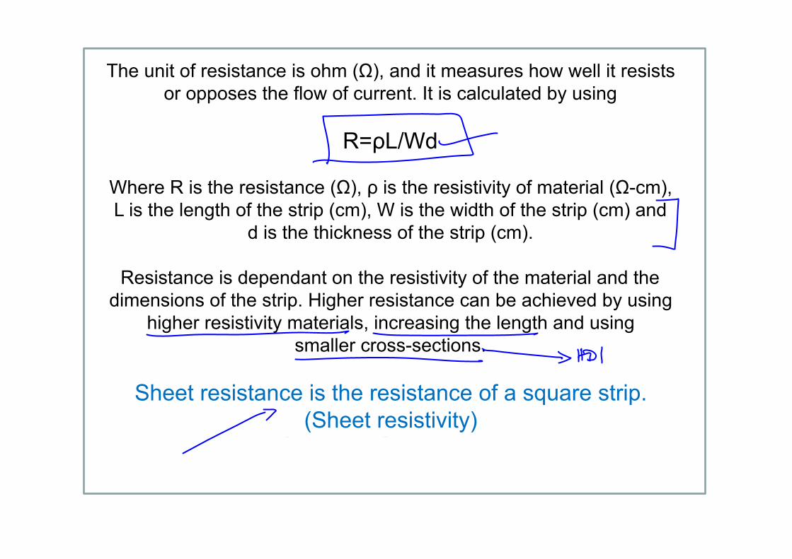
The unit of resistance is ohm (!), and it measures how well it resists or opposes the flow of current. It is calculated by using
R="L/Wd
Where R is the resistance (!), " is the resistivity of material (!-cm), L is the length of the strip (cm), W is the width of the strip (cm) and
d is the thickness of the strip (cm).
Resistance is dependant on the resistivity of the material and the dimensions of the strip. Higher resistance can be achieved by using
higher resistivity materials, increasing the length and using smaller cross-sections.
Sheet resistance is the resistance of a square strip.
(Sheet resistivity)

N2=1 N3=1
Source: Richard Ulrich et al; Swapan Bhattacharya; other
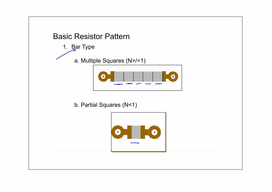
Basic Resistor Pattern 1. Bar Type
a. Multiple Squares (N>/=1)
b. Partial Squares (N<1)

2. Meander Type A meander resistor can be considered as a bar resistor with the
exception of the corner squares (right-angle bends). Due to the change in current density at right-angle path, the effective number of square is 0.56.
Source: Richard Ulrich; Swapan Bhattacharya, Ohmega Inc
Example: Sheet resistance Rs= 100ohms/square No. of squares=37 No. of corner squares-16 Total no. of effective squares= 37+(16 x 0.56)
= 45.9 ~46
Resistance value= 46 x 100= 4.6Kohms
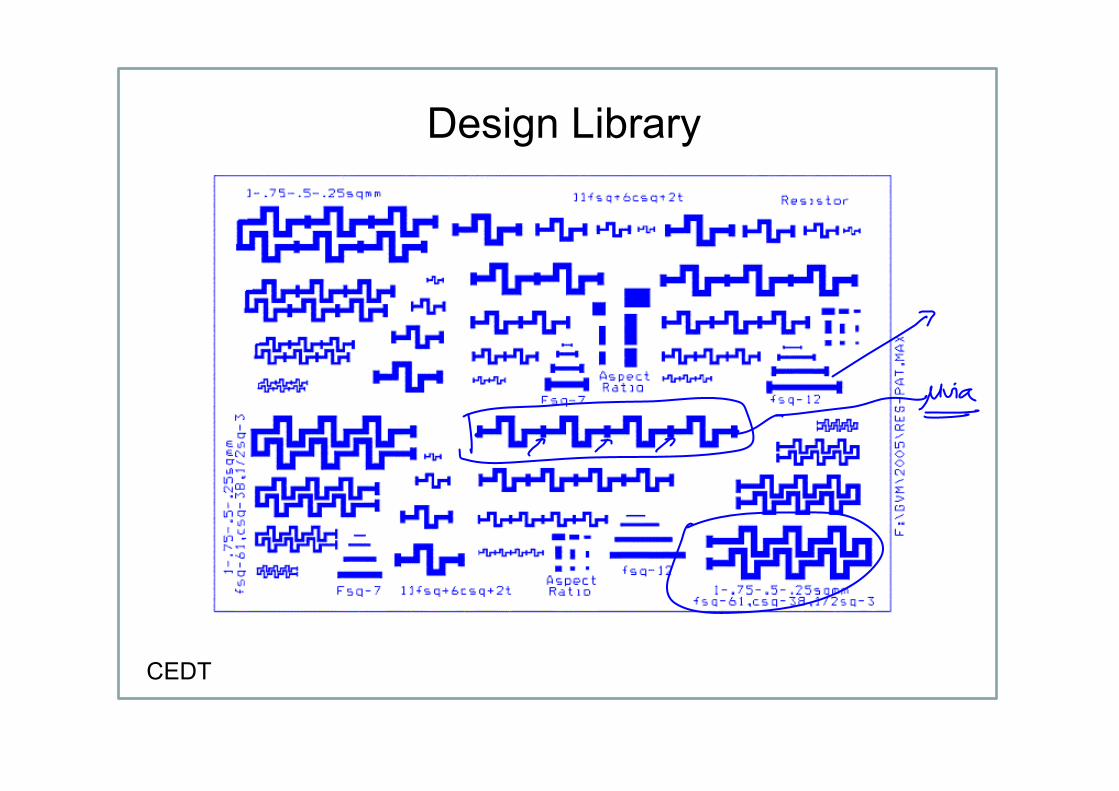
Design Library
CEDT

Embedded Passives Design, Fab and Test

Technology Approach
Electroless plated Resistor Process (1-1Kohm)
1. Synthesis of Ni-P alloys by electroless deposition on dielectrics 2. Electroless plated resistor on epoxy and other polymers (Proprietary chemicals/lab synthesis)
Foil Transfer Process (1-1Kohm) SUBTRACTIVE PROCESS
1. Lamination using commercially available resistor foils 2. Laminated thin film resistors on BCB and epoxy dielectrics (Ohmega/Shipley/Gould)
Polymer thick film (PTF) Printing Process (500-10Kohms) ADDITIVE PROCESS
1. Stencil printing using commercial products 2. Lift off Process (Asahi Chemical/Motorola/DuPont)
ROUTES TO EMBEDDED RESISTORS
Issues Laser Trim for better tolerance in R values
Screen printing of PTF is technician and machine dependant; parameters not always reproducible Choice of Substrate critical for foil transfer process due to Tg and lamination temperatures
Electroless Ni-P alloy plating consistency depends on pH, temperature and P concentration in bath

Steps for fabrication of Embedded R by PTF
• Polymer-carbon thick films with suitable sheet resistivity can be used • Stencil printing; screen printing or masking by dry film photoresist
Source: KJ Lee, Georgia Tech
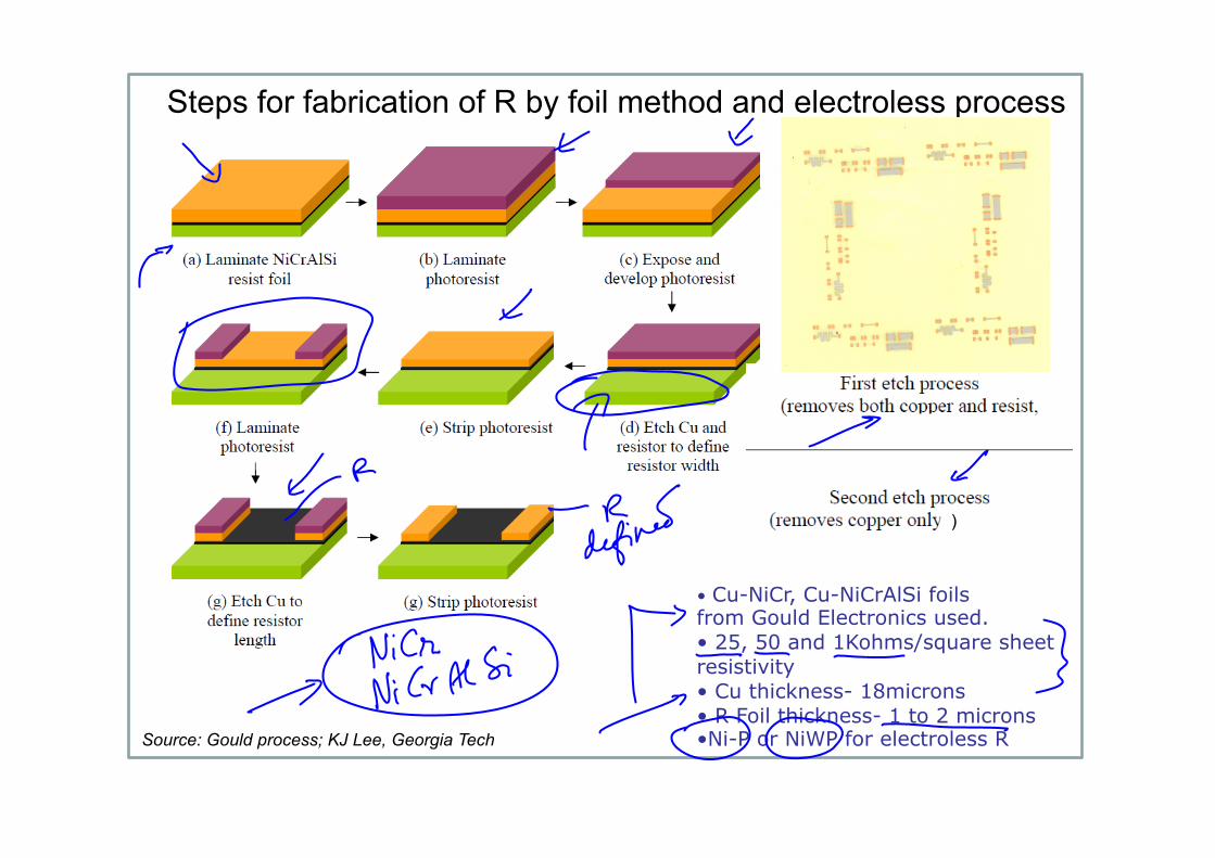
Steps for fabrication of R by foil method and electroless process
• Cu-NiCr, Cu-NiCrAlSi foils from Gould Electronics used. • 25, 50 and 1Kohms/square sheet resistivity • Cu thickness- 18microns • R Foil thickness- 1 to 2 microns • Ni-P or NiWP for electroless R Source: Gould process; KJ Lee, Georgia Tech
)

Electroless Bath Formulations for Ni-P • Sodium Acetate Bath • Sodium Pyrophosphate bath • Sodium Citrate Bath
Sodium Acetate Bath Composition Nickel Sulphate : 30 g/l Sodium Hypophosphite : 15 g/l Lead Acetate : 0.015 g/l Sodium Acetate : 15 g/l Temperature : 90°C pH : 4-5
Sodium Pyrophosphate bath Composition (Solution A & B mixed in equal Proportions) Solution A Nickel Sulphate : 50 g/l Sodium Pyrophosphate : 100 g/l 25 %Ammonium Hydroxide : 200 ml/l Solution B Sodium Hypophosphite : 50g/l Temperature : 30°C pH : ~11
Sodium Citrate Bath Composition Nickel Sulphate : 26.3 g/l Sodium Hypophosphite : 21.2 g/l Trisodium Citrate : 58.8 g/l Temperature : 90°C pH : 4-5
Ni-W-P Composition Nickel Sulphate : 7 g/l Sodium Hypophosphite : 10 g/l Sodium Tungstate : 10 g/l Trisodium Citrate : 45 g/l Temperature : 90°C pH : 4-5
Observations • In the Citrate bath, lowering of the concentration of chelating agent, increases the R value. • Time, temperature and pH critical to the nature of the deposit.
• Reducing Agent- Sodium Hypophosphite Chelating Agents used:


