
IMPROVED BUFFERLESS ROUTING VIA BALANCED PIPELINE STAGES
By
Jianshu Qian
Thesis
Submitted to the Faculty of the
Graduate School of Vanderbilt University
in partial fulfillment of the requirements
for the degree of
MASTER OF SCIENCE
in
Electrical Engineering
August, 2013
Nashville, Tennessee
Approved:
Professor William H. Robinson
Professor Yuan Xue

i
ACKNOWLEDGEMENTS
First of all, I would like to express my gratitude to my advisor, Dr. William H. Robinson,
for his encouragement and guidance during the period while I pursued my Master’s
degree at Vanderbilt University. He is not only an advisor for my research, but also the
mentor for my life.
Also, I am deeply grateful to my committee member, Dr. Yuan Xue, for her support in
reviewing this thesis. I would like to thank all the members in the Security and Fault
Tolerance (SAF-T) Research Group for sharing their ideas and feedback with me since I
joined.
Last but not least, I must thank my parents. They encourage me so much that when I
meet difficulties, no matter how big they are, I never lose hope and at last I can overcome
them.

ii
TABLE OF CONTENTS
Page
ACKNOWLEDGEMENTS ............................................................................................................... i
TABLE OF CONTENTS .................................................................................................................. ii
LIST OF FIGURES ........................................................................................................................... iv
LIST OF TABLES .............................................................................................................................. v
Chapter
I. INTRODUCTION........................................................................................................................... 1
Network-on-Chip History .........................................................................................1
Motivation and Our Approach ..................................................................................2
Thesis Organization ..................................................................................................4
II. BACKGROUND ........................................................................................................................... 5
Network-on-Chip......................................................................................................5
Virtual-Channel Router architecture .........................................................................9
Bufferless Deflection Routing ................................................................................ 10
CHIPPER ............................................................................................................... 11
Injection .......................................................................................................... 12
Microarchitecture ............................................................................................ 12
Ejection ........................................................................................................... 14
Golden Packet ................................................................................................. 15
Field Programmable Gate Array (FPGA) ......................................................... 15
III. REDESIGN OF THE PERMUTATION STAGE ............................................................... 18
IV. RESULTS AND DISCUSSION ............................................................................................. 22
Methodology ......................................................................................................... 22
Router’s Operating Frequency ............................................................................... 23
Area ...................................................................................................................... 24
Power .................................................................................................................... 25
Latency.................................................................................................................. 27

iii
V. SUMMARY AND FUTURE WORK ..................................................................................... 29
REFERENCES .................................................................................................................................. 30
APPENDIX……………………………………………………………………………………………….33
iv
LIST OF FIGURES
Figure 1 Examples of communication structures in Systems-on-Chip ..............................6
Figure 2 NoC topologies .................................................................................................7
Figure 3 The typical VC router architecture ................................................................... 10
Figure 4 Two-stage permutation with four arbiters ........................................................ 13
Figure 5 FPGA design flow .......................................................................................... 17
Figure 6 4x4 mesh networks ......................................................................................... 17
Figure 7 Improved router structure................................................................................ 20
Figure 8 Timing path ..................................................................................................... 23
Figure 9 Dynamic and Static power consumption for each router .................................. 26
Figure 10 Flit average latency ....................................................................................... 27
Figure 11 The latency information for each router ........................................................ 27

v
LIST OF TABLES
Table 1 Flit structure ........................................................................................................9
Table 2 Steering functions for two-stage permutation structure .................................... 13
Table 3 Data structure stored in two memory blocks ..................................................... 22
Table 4 Critical path for each stage observed by Quartus II ........................................... 24
Table 5 Number of logic elements for each router ......................................................... 24

1
CHAPTER I
INTRODUCTION
I.A Network-on-Chip History
As very-large-scale integration (VLSI) technology advances, designers aim to build more
complex and robust computing systems in a single silicon chip [1]. With the rapid
increase of the number of components that appear on the chip, interconnect requirements
have also increased; in fact, interconnect becomes a strict limitation on performance [2].
In order to solve this problem, the packet–switched on-chip network has been proposed
[3]. The idea of a Network-on-Chip (NoC) borrows networking theory from the computer
networking domain and considers each intellectual property (IP) core as a single node. In
each node, a high-speed router connects with other routers of neighboring nodes [4].
At the heart of the on-chip network, the tradeoff between performance, area, and
power is significant [4]. In previous studies [5-7], the router architecture always contains
buffers on the input ports. The buffer scheme is used to store packets; these packets must
wait for the output resource due to contention with other packets [8]. These designs have
been widely adopted due to their improved performance [3]. However, the analysis of
different hardware implementations showed that the networks consisting of buffered
routers are expensive. In the TRIPS prototype processor [9], 75% of the NoC area is
filled with buffers; for the RAW microprocessor [10], 36% of chip power is consumed by
the on-chip network. Hence, the buffer space issue has been deeply discussed, and the

2
trend of design efforts has shifted. Some related studies [11-13] attempt to identify an
optimal buffer size to reduce the cost associated with the hardware.
Finally, the extreme idea - entirely bufferless routing - has been proposed in
BLESS [14] and improved by CHIPPER [15]. Bufferless routing is borrowed from
network theory and has been called “hot potato” routing. Because the networks have no
buffer to store the packets, each packet has to keep moving through the network until it
reaches its destination [14]. When two packets contend for the output resource, one
packet has to deflect, which causes it moves further away from its destination [14]. The
key for performance in bufferless routing is minimizing the deflection rate. In CHIPPER,
the results show that bufferless routing saves 169% for area [16] and averages 54.9% less
power consumption compared to the buffered networks in Chip Multiprocessors (CMP)
[15]. However, when the networks have a high injection rate of packets, the conventional
buffered network has a greater performance [17].
I.B Motivation and Research Approach
In the ideal case, the bufferless router should produce a deflection rate as small as
possible. A smaller deflection rate means that the network has lower average packet
latency [17]. CHIPPER has a two-cycle router pipeline structure, and the permutation
structure in the second stage of CHIPPER is used to allocate the output resource [15].
With an investigation of the permutation, it was observed that the permutation cannot
meet the requirement of minimizing the deflection rate (i.e., some packets are deflected
unnecessarily). This feature also indirectly increases the total power consumption. In
order to reduce the average packet latency, an improved design is proposed for CHIPPER

3
without changing the router’s speed. The original permutation in the second stage is
replaced with a new permutation. The critical path in the new second stage is a little
longer than the previous second stage, but maintains the original speed of CHIPPER; the
original architecture of CHIPPER used a two-stage pipeline structure where the first stage
was significantly longer. Thus the router’s frequency was determined by the first stage.
This new design uses the available slack time within CHIPPER’s operating frequency,
and the delay of the second stage is still less than the first stage. Moreover, according to
the observation in minBD [16], CHIPPER with two ejection port increases the average
performance by 3.7% over the original CHIPPER. Hence in this research, dual-ejection
CHIPPER is considered as baseline for comparison.
In the hardware implementation, the use of a field-programmable gate array
(FPGA) is reasonable. FPGAs are a way to build and verify complex systems with high
integration levels. Various logic elements, memory blocks and I/O allow us to design the
on-chip network rapidly [18]. In this research, the FPGA provides the capability to
determine the maximum frequency from the critical path. It also offers a platform
allowing us to build the on-chip network in order to measure the average packet delay.
This thesis describes the experience in designing a real-time mesh topology network with
the new bufferless router and compares the results between dual-ejection CHIPPER and
the improved router design. The results show that the improved router structure reduces
the deflection rate significantly, and reduces up to 16.2% average latency than the Dual-
ejection CHIPPER. The operating frequency for both designs is the same.

4
I.C Thesis Organization
The rest of the thesis is organized as follows. Section II provides the necessary
background on NoC, traditional buffered router, baseline CHIPPER, and the FPGA
design flow. Section III presents the improved router structure. Section IV discusses the
evaluation methodology and results. Section V summarizes this thesis and discusses the
future work.
5
CHAPTER II
BACKGROUND
This chapter introduces the basic ideas of NoC, traditional buffered router and bufferless
deflection routing, outline the CHIPPER structure briefly, and describe the design flow
when we use an FPGA board to build the 4x4 mesh network.
II.A Network-on-Chip
“The chip is the network [19].” This idea proposed by Radu Marculescu and Paul
Bogdan points out the direction of on-chip interconnection. Previous studies [1, 20, 21]
have expounded that many industrial tasks can be solved by a System-on-Chip (SoC)
platform and many industrial products that implement this method appear in the market,
especially in the CMP domain. SoC integrates all components of a system into a small
single chip, and it can consist of microcontrollers, microprocessors, DSPs, memory
blocks, and I/O. As VLSI technology advances and demand for performance increases,
the designer desires to add more IP cores onto a single chip. However, significant
limitations have arisen as we continue to implement traditional interconnects.
In Figure 1, it shows three kinds of on-chip interconnect structure for a mobile
phone [22]. The bus topology and the point-to-point (p2p) topology have their own
strengthes and weaknesses. Both of them have well-understood concepts and
comprehensive research experience. These strengthes reduce the production period
efficiently. In a simple mobile phone system, implementing a bus or p2p interconnect is
reasonable. However, as more IP cores are connected on the single chip, they become the

6
limitation for communication. As more units are added to busses, because of the parastic
capacitance, the power consumption for each communication event grows as well.
Moreover, shared busses create contention and hierachal busses result in complexity [22].
For the p2p structure, the number of wires has an exponential increase as the designer
adds more IP cores on a chip. It results in both a routing problem and a die area problem.
In order to solve these problems, the NoC structure has been proposed. NoC appiles a
networking method, and the IP core implements the on-chip communication by a router
just like how the terminal works in the real world. Unlike busses and p2p, it is the first
time that the networking method is involoved in the digital system design, and compared
to networking, the digital system design focuses on the distinct parameters. Designers are
not only concern about latency, but also care about power consumption and area. Hence,
NoC is still considered as an immature area and maintains rapid growth.
Figure 1 Examples of communication structures in Systems-on-Chip. a) traditional bus-
based communication,b) dedicated point-to-point links, c) a chip area network. [22]
As the designer implements an on-chip network, the network is characterized by:
(1) topology, (2) routing, (3) flow control, and (4) router structure.

7
Usually, we consider the IP core and its corresponding router as one node, and the
distribution of nodes is specified by topology. Fortunately, networking engineers have
designed various topologies, such as Mesh, Torus, Octagon, and Butterfly Fat Tree (BFT)
[23]. Figure 2 shows the different topologies. The most popular topology in NoC is mesh,
and in this thesis, we consider it as our default topology.
Figure 2 NoC topologies. (a) Mesh, (b) Torus, (c) Octagon, (d) BFT. [23]
8
Routing determines the path between the initial node and the destination.
Traditional routing is deterministic and use minimal routing. The path for each packet has
been decided before being sent into the network, and their path is absolutely minimal.
The node position is described using a coordinate system. For example, suppose a packet
whose start position and destination are neither in the same row nor in the same column.
The X-Y rule is considered as the most common routing rule in NoC. It determines that a
packet goes through x-axis first after being sent into network, until its current position is
in the same column with the destination. Then it will go through the y-axis until it
reaches its destination. The X-Y rule has been acknowledged by every router in the
network, and that promises all packets in the network have minimal path. However, since
the path for each packet is unchangable, for each node, it is highly probable that more
than one packet will contend in the same direction. In this case, in order to store the rival
packet, adding buffers on the input port has been proposed in router architecture. The
buffered router structure is disscussed further in Section II.B. An opposite routing method
is adaptive routing. The path for each packet is highly based on the real-time traffic in the
network. If the conjestion happens in a part of network, then the packet would take a
detour. The advantage of this method is that the buffer structure is unnecessary. However,
the minimial path cannot be guaranteed. Bufferless deflection routing is a kind of
adaptive routing, which is disscussed in Section II.C.
Flow control determines the basic unit in the network, the link carrying capacity,
and the buffer capacity if necessary. A complete packet that traverses the network is
unrealistic since the size of packet is not uniform. A packet is typically divided into a
couple of flits, and the flit is the basic unit in the network. The size of the flit determines

9
the carrying capacity for a link and the buffer size. Table 1 illustrates the basic flit
structure, where each flit consists of the Information, Destination address, and Unique ID.
Table 1 Flit structure
In a simple router, the essential components are inputs, outputs, and a switch. A
typical router has five inputs/outputs: four that connect with neighbor routers and one that
connects with the local IP core. The switch is used to allocate the output resources. As for
other components, it highly based on what kind of routing is selected. Section II.B
discusses a type of buffered router structure, while Section II.C and Section II.D discuss a
type of bufferless router structure.
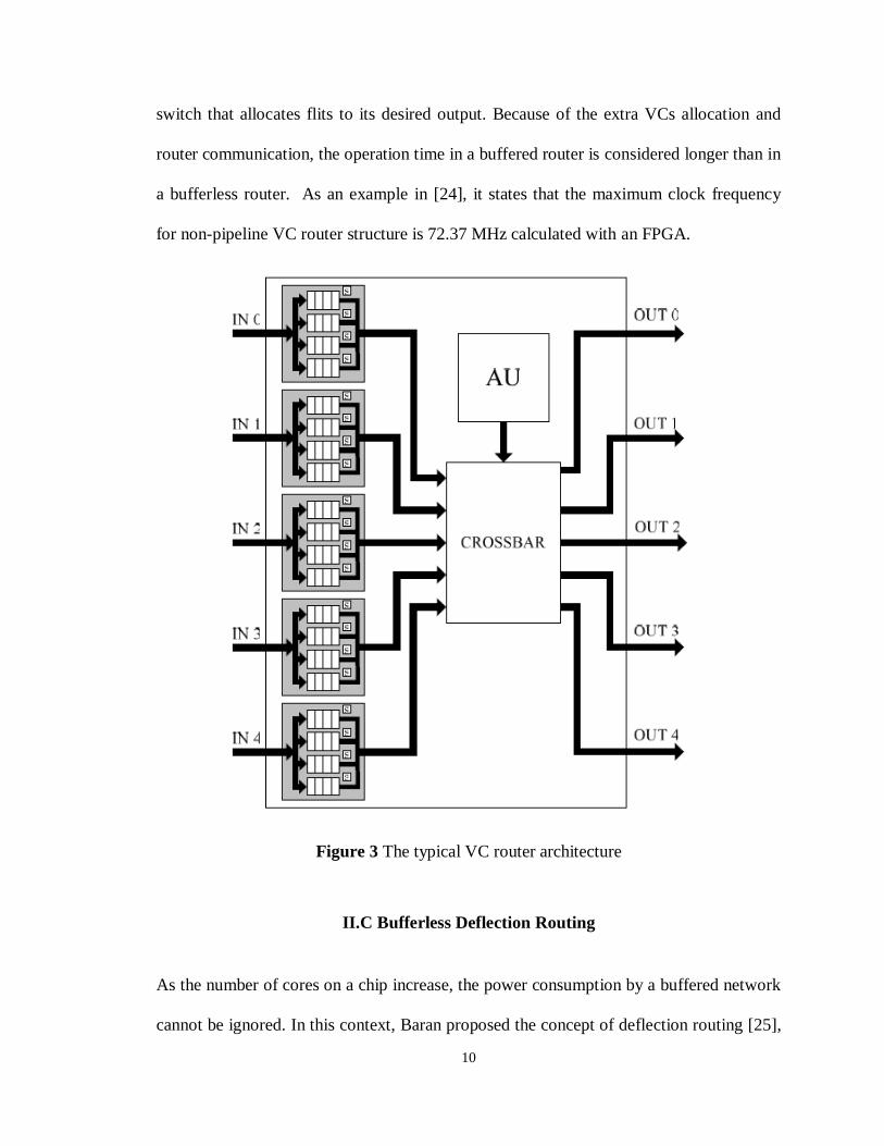
II.B Virtual-Channel Router Architecture
The Virtual-Channel (VC) router is a popular structure in the NoC that applies
deterministic and minimal routing. Even through there are a lot of various structures that
are derived from the VC router structure, the base structure adds buffers at each input
port. Figure 3 shows the base VC router structure. In this case, four VCs at each input
port are buffered in first-in-first-out (FIFO) queues. In order to acquire the states in
neighboring routers, the router communicates with its neighbor routers all the time. If all
the VCs in one input port are full, then its corresponding neighbor would stop
transferring flits to that input until there is an empty VC in that input port. This
communicated operation is controlled by an Arbitration Unit (AU). The crossbar is a
Information Destination Address Unique ID
10
switch that allocates flits to its desired output. Because of the extra VCs allocation and
router communication, the operation time in a buffered router is considered longer than in
a bufferless router. As an example in [24], it states that the maximum clock frequency
for non-pipeline VC router structure is 72.37 MHz calculated with an FPGA.
Figure 3 The typical VC router architecture
II.C Bufferless Deflection Routing
As the number of cores on a chip increase, the power consumption by a buffered network
cannot be ignored. In this context, Baran proposed the concept of deflection routing [25],

11
and the first implementation for an on-chip network is BLESS [14]. Compared to the
typical virtual channel buffered network, eliminating buffers can save significant die area
and power [15]. It was considered as an alternative scheme for buffered routing.
In the BLESS and CHIPPER networks, each packet splits its resource into several
flits, and the flit as the basic unit moves through the network independently [16]. As a flit
injects into the network, it has to keep moving and cannot stop until it has been ejected
from the network. The Unique ID field is necessary because the flit travels through the
network independently, and the deflection is unpredictable; flits from the same packet do
not arrive at the destination in order. The Unique ID is used to sort flits at the local node;
when a packet has completely arrived, the node will send it to the processor. Then the
network must provide buffer space at the exit of each node in order to reassemble the
packet.
The deflection algorithm is very simple. In the ideal case, if two flits arrive at the
router at the same cycle and their desired output is not the same, then they will move away
from this router towards their desired output. However, if two flits contend for the same
output, then one flit will win and the other flit has to move away from this router towards
a free output.
II.D CHIPPER
CHIPPER was an improved design that was derived from BLESS. Compared to BLESS,
CHIPPER provided a more reasonable permutation structure and packet reassembly. In
the following content, the basic principles of CHIPPER are described.
12
II.D.1 Injection
The injection port is the entrance that allows the flit into the network. However, the
bufferless router cannot guarantee that every fresh flit would be injected into the network
immediately. Injection was only permitted when the inputs have a free slot. Therefore, a
buffer space in the injection port is necessary. The buffer is used to hold the fresh flit
when the injection requirement was not met.
II.D.2 Microarchitecture
The baseline CHIPPER implements a two-stage router pipeline structure. The first stage
is a computation stage. In this stage, the function is not only ejecting and injecting flit,
but also computing the desired output based on the destination address. The desired
output is based on: (1) analysis of the X-Y routing and (2) comparisons of the destination
address with the local address. Because the router is bufferless, after the computation
stage, the flit is stored in the register and waits for the permutation stage [15].
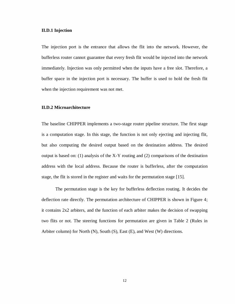
The permutation stage is the key for bufferless deflection routing. It decides the
deflection rate directly. The permutation architecture of CHIPPER is shown in Figure 4;
it contains 2x2 arbiters, and the function of each arbiter makes the decision of swapping
two flits or not. The steering functions for permutation are given in Table 2 (Rules in
Arbiter column) for North (N), South (S), East (E), and West (W) directions.
13
Figure 4 Two-stage permutation with four arbiters [15]
Table 2 Steering functions for two-stage permutation structure [15]
Input Rules in Arbiter Output
Flit (desired
direction)
Stage 1
(Arbiter1 and
Arbiter 2)
Stage 2
(Arbiter3 and
Arbiter4)
Permutated
Input
Output
Direction
Flit 1(E)
Flit 2(N)
N, S: output 0
E,W: output 1
N, E: output 0
S, W: output1
Flit 2(N)
Flit 3(S)
N
S
Flit 3(S)
Flit 4(W)
N, S: output 0
E,W: output 1
E, N: output 0
W, S: output1
Flit 1(E)
Flit 4(W)
E
W
N
S
E
W
Stage 1 Stage 2
Output 1
Output 0
For each arbiter

14
In Table 2, Flit 1 (requires East direction) and Flit 2 (requires North direction)
enter into Arbiter 1 (Figure 4, top left); based on the rules, the arbiter decides that these
two flits should swap. Flit 3 (requires South direction) and Flit 4 (requires West direction)
enter Arbiter 2 (Figure 4, bottom left); Arbiter 2 decides that they do not swap. After Flit
1 and Flit 3 have been swapped in the middle between the two stages, Flit 2 and Flit 3
enter into Arbiter 3 (Figure 4, top right), Flit 1 and Flit 4 enter into the Arbiter 4 (Figure 4,
bottom right), and the arbiters decide the next routing assignments. Finally, the four flits
get to their desired directions. Compared to the earlier BLESS design, the two-stage
permutation structure implements the parallel arbiter scheme in both stages, which
divides the critical path efficiently [15]. Even though the result shows that the
performance of CHIPPER is lower than BLESS, since the critical path of CHIPPER is
reduced by 29.1% over BLESS, that guarantees CHIPPER is better than BLESS [15].
II.D.3 Ejection
The ejection port is the exit that sends the flit out of the network. As previously
discussed, in order to maintain the packet’s correctness, the network must provide a
reassembly buffer at each node.
The analysis of the minimally buffered deflection routing (MinBD) shows that in
up to 8.5% of all cycles, two flits reach the destination router in the same cycle [16]. In
this case, if the design only supports ejecting a single flit per cycle, then it will produce
one unnecessary deflection. In order to reduce the deflection rate, we implement a dual-
ejection design in both CHIPPER and our improved router. That means these two

15
schemes could eject two local flits in a single cycle. The result shows CHIPPER with two
ejection increases average performance by 3.7% over the original CHIPPER [16].
II.D.4 Golden Packet
The golden packet idea is used as an inexpensive strategy for priority to guarantee against
the livelock problem. Livelock is a common problem that occurs in bufferless deflection
routing networks. When a flit injects into the network, the deflection behavior is
unpredictable. If the deflection happens, then the flit can move further away from its
destination. In the worst case, an unlucky flit will be deflected forever and never reach its
destination. Moreover, the livelock problem will cause the reassembly buffer to overflow
at the destination node. It is because other flits that belong to the same packet have to
wait for the missing flit.
In CHIPPER, to avoid the livelock problem, the network selects a single packet
and sets this packet as the Golden priority. For a period time, the priority of this packet is
above all other packets globally. All routers in the network have this knowledge. The
period must ensure that all flits belonging to the golden packet reach their destination. In
the every permutation, this prioritization rule was added into every arbiter. If a golden flit
is the input, then it will win over any non-golden flits. This implementation guarantees
the golden packet will not be deflected except if both flits belong to the golden packet.
II.D.5 Field Programmable Gate Array (FPGA)
In this section, the FPGA design flow is introduced. An FPGA is a good way to verify a
digital system’s design before silicon manufacturing. It is an integrated circuit that

16
contains programmable logic elements with reconfigurable interconnections. Users
configure the logic elements to perform various functions. Modern FPGAs also support
memory block and IP cores. These features offer users a rapid design process [26].
In this thesis, the Altera FPGA DE2-115 board (with a Cyclone IV EP4CE115F29
FPGA) [27] is used to perform the investigation on CHIPPER and build a 4x4 mesh
topology network with the bufferless routers. This FPGA board contains approximately
115,000 logic elements and 138M memory blocks [27]. The network was developed with
the VHDL language; simulation and synthesis of the design use the Electronic Design
Automation (EDA) tool Quartus II [28], and the function was verified at the gate level
with ModelSim [29]. The design flow is shown in Figure 5 [30]. Power consumption and
critical path information are produced by the PowerPlay function and the TimeQuest
function in Quartus II. Quartus II also provides a function called In-System Memory
Content Editor. It is an easy way to observe the content that has been stored in the
memory block [28].
In order to evaluate the average latency, SRAM is used in each node to build two
memory blocks. The SRAM is not included in the analysis of the critical path. One
memory block is used to connect with the injection port and store the injection flits; the
other one is used to connect with the two ejection ports and records the flits and the time
they were ejected from the local node. Figure 6 shows the 4x4 mesh topology network as
well as the components contained in each node.

17
Figure 5 FPGA design flow [30]
Figure 6 4x4 mesh networks

18
CHAPTER III
REDESIGN OF THE PERMUTATION STAGE
During the investigation for CHIPPER, it was observed that the critical path between the
computation stage and the permutation stage is unbalanced. Because the router is a two-
stage pipelined architecture and the permutation stage is faster than the computation
stage, it gives the opportunity to improve the architecture. Moreover, the permutation in
CHIPPER cannot meet the ideal case; some unnecessary deflections of flits occur in
CHIPPER. For example, assume four flits enter into the router, and their desired
directions are N, S, E, and W, respectively. Meanwhile, the outputs have the same order
with their desired directions. In the ideal case, the flits can move through the router with
their desired directions. However, in CHIPPER, two flits must be deflected in this
situation. Because the critical path in the permutation stage is shorter than the critical
path in the computation stage, there is timing slack to improve the permutation so long as
the critical path is not longer than computation stage.
It was decided to keep the 2x2 arbiter scheme and modify their rules to achieve
the idea to improve the design. Moreover, an extra component is added following the 2x2
arbiter. The extra component, which is called Final Chance, will increase the critical path
in the permutation stage. The critical path in the new permutation stage is nearly equal to
the critical path in the computation stage. The improved design is shown in Figure7, and
the critical path information is discussed further in Section IV.2.

19
Algorithm 1. Improved permutation steering algorithm
Improved permutation
Since the order for flits maybe change, we describe
them with flits in position 1, 2, 3 and 4 from top to
bottom, and the corresponding desired directions are
d1, d2, d3, d4
Assuming the output direction is N, S, E, and W
If one input slot is empty, the desired direction is 0
Arbiter 1 if (d1 == N or S) or (d2 == E or W)
do none
else
do swap
Arbiter 2 if (d3 == N or S) or (d4 == E or W)
do none
else
do swap
swap flits that are in position 1 and 2
Arbiter 3 if (d1 == N) or (d2 == S)
do none
else
do swap
Arbiter 4 if (d3 == E) or (d4 == W)
do none
else
do swap
Final Chance
If (d1 != N)
if (d3!=E and d1! =0 and d3!=0)
do swap flits that are in position 1 and 3
else if (d4!=W and d1!=0 and d4!=0)
do swap flits that are in position 1 and 4
else if (d2 != S)
if (d3!=E and d2! =0 and d3!=0)
do swap flits that are in position 2 and 3
else if (d4!=W and d2!=0 and d4!=0)
do swap flits that are in position 2 and 4
20
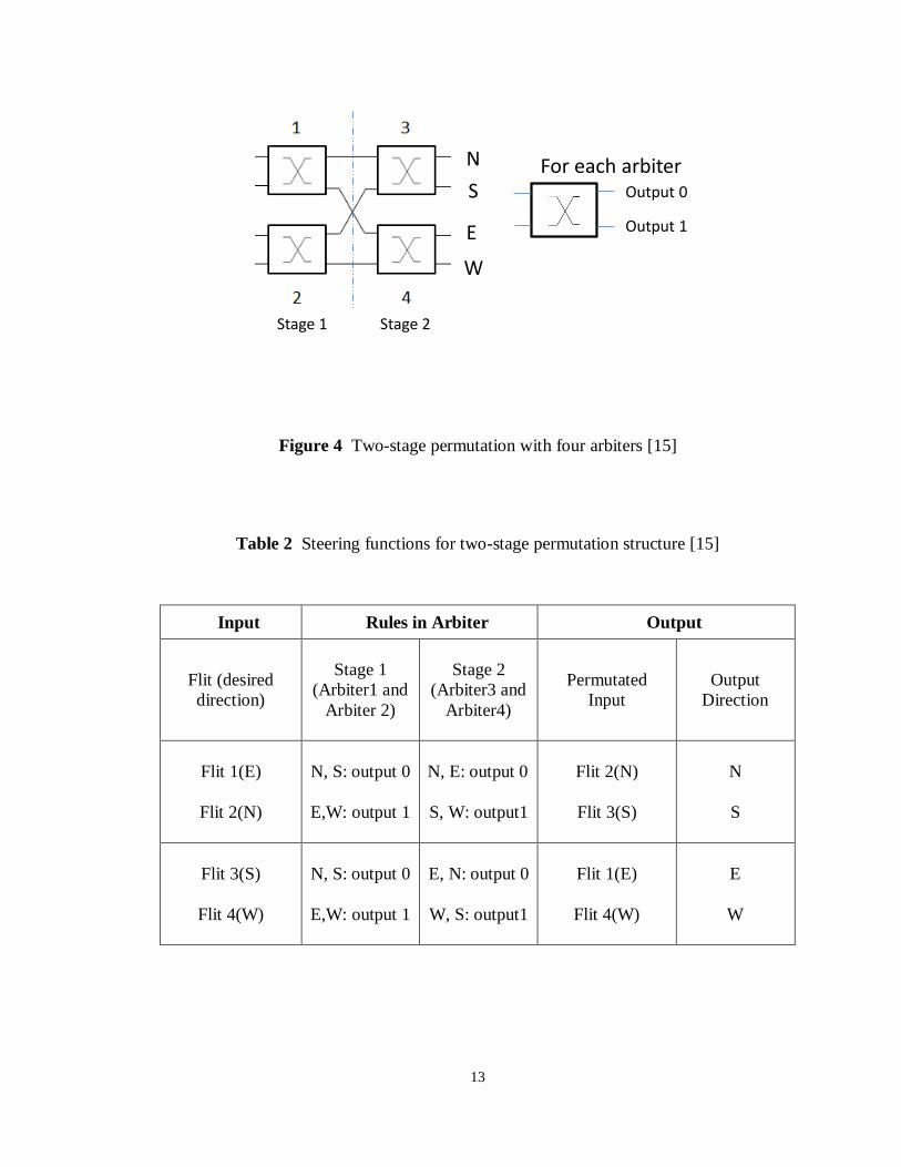
Figure 7 Improved router structure
Because the rules for golden packet are easy to understand, we do not include
them in Algorithm 1. The rules described in Algorithm 1 only demonstrate normal cases.
The Final chance component give flits a last chance to swap. It is assumed that the order
of the outputs is N, S, E, and W. The function for the first two arbiters is to move flits
that desire N or S to the Arbiter 3 and to move flits that desire E or W to the Arbiter 4.
Next, based on the rules, Arbiter 3 and Arbiter 4 decide to swap them or not. They
guarantee at least one flit will win its desired output. Finally, inputs move through to the
Final Chance step. This step only affects the flits that will be deflected. The two flits that
will be deflected swap with each other. The previous example is used to demonstrate this
permutation. Assume that the desired directions of four flits are N, S, E and W from top
to bottom, and the output order is N, S, E, and W. Within the 2x2 arbiter structure, Flit 2
and Flit 3 have changed their order and the order for desired directions has

21
simultaneously changed to N, E, S, and W. The router discovers that Flit 2 and Flit 3 will
be deflected, and then the router gives them a final chance to swap with each other. The
final result order is N, S, E, and W, and no deflection happens in this case.
When the function of permutation is analyzed, we implement probability theory
and consider the inputs as a combination. The desired direction for each input has five
possibilities: N, S, E, W, and if the input is empty, we assume the desired direction is 0.
Because each router has four inputs, there are 625 combinations. The improved router
improves 145 combinations. If the extreme case is considered (i.e., no input is empty, as
would occur when the network has a high injection rate), then the improved combination
number is 94 over 256 (i.e., the maximum number of combinations).

22
CHAPTER IV
RESULTS AND DISCUSSION
In this thesis, the goal is to improve CHIPPER and to implement the new algorithm with
an FPGA board. A 4x4 mesh topology network was implemented to test the design. The
improved router was compared to a dual-ejection CHIPPER using two metrics: average
latency and hardware cost (i.e., area and power). Both results were produced by the
FPGA and Quartus II.
IV.A Methodology
To evaluate the average latency, we collect the uniform input set from simulator NS-3.
NS-3 is a discrete-event network simulator that is used to evaluate Internet systems [31].
The data are pre-loaded into the memory block that is connected with an injection port in
each node. The basic flit is 32 bits. It consists of 10 bits for the Unique ID, 4 bits for the
destination address and 16 bits for the resource. As a flit moves away from the network,
the Unique ID and the time it arrives in the destination are recorded in another memory
block.
Table 3 Data structure stored in two memory blocks
16 bits Resource 4 bits Address 10 bits Unique ID
10 bits Time Info. 4 bits Address 10 its Unique ID

23
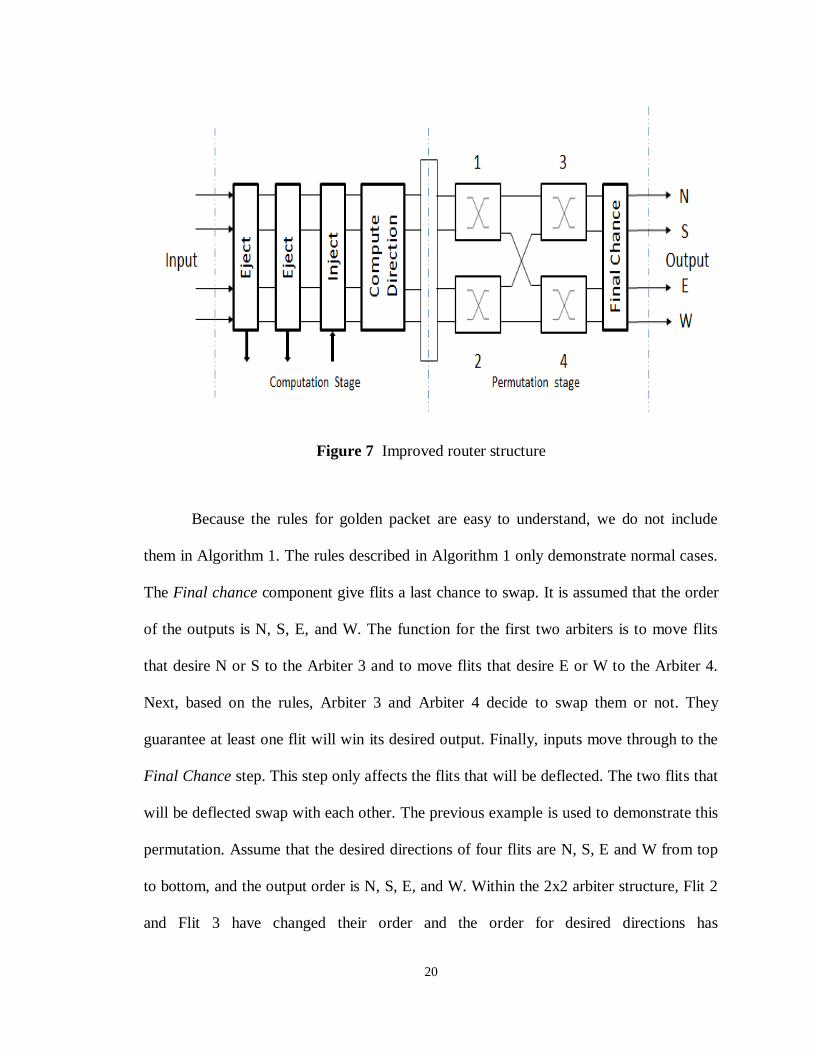
IV.B Router’s Operating Frequency
First, we study the impact of our changes on the operating frequency of the router.
TimeQuest is the function for analyzing timing. It determines the reliable conditions
during which the integrated circuits can be operated properly.
Figure 8 Timing path
In Figure 8, it illustrates the timing path in a simple circuit. The TimeQuest
requires the design to produce a timing netlist. Next, based on the timing netlist, the
TimeQuest decides the data required times, data arrival times, and clock arrival times and
detects possible timing violations. Moreover, it determines the timing relationships that
must be met for the design. After these operations, the TimeQuest determines a longest
time path in the circuit. In order to operate properly, the clock frequency is determined by
the longest timing path in the circuit, called the critical path. Using this function on
Quartus II, we observe the critical path. Table 4 shows the critical path for each stage and
the maximum clock frequency for each router.
24
Table 4 Critical path for each stage observed by Quartus II
Dual-ejection
CHIPPER Improved Router
First
stage
Second
stage
First
stage Second stage
Critical Path 3.22 ns 2.34 ns 3.22 ns 3.20 ns
Maximum Clock
Frequency 310.6 MHz 310.6 MHz
From the table, we find the critical path in the improved second stage increased
by 36.8% over the original second stage, but the improved second stage is more balanced
with the critical path of the first stage. The maximum clock frequency is determined by
the longest critical path in each router. Because the critical path for the first stage is 3.22
ns in each router, the maximum clock frequency for both designs is 310.6 MHz. So, our
improved router has the same speed as the Dual-ejection CHIPPER.
IV.C Area
Table 5 Number of logic elements for each router
Dual-ejection CHIPPER Improved Router
Logic Element 529 645
Next, Table 5 shows the area impact with the number of logic element used by the
Cyclone IV FPGA on the DE2-115 board. It displays the number of logic elements for
each router. The increased router area (22%) from Dual-ejection CHIPPER to the

25
improved router is due to adding the Final Chance component in the second stage. Since
the CHIPPER has a significant saving in area (169%) compared to the conventional
buffered router (4 virtual channels (VCs), 4 flits per VC) [16], the increased area in the
improved router still provides significant savings when compared to buffered routing.
IV.D Power
The Powerplay Power Analysis Tool is the function used to simulate the power
consumption within the Quartus II software. There are a lot of factors affect the results.
The most obvious factor for power consumption is the device resource usage. It is
apparent that a design with more logic elements (LEs), multiplier elements, and memory
blocks would consume more power. The FPGA device is another factor for power
consumption. Many device parameters can affect the power consumption. Manufacturing
process is an instance. Process impacts static power consumption primarily since sub-
threshold leakage current varies exponentially with changes in transistor threshold
voltage [28]. But the impact for dynamic power is trivial. To avoid the false comparative
result, we must clarify the FPGA device before we compare the power consumption.
Environmental condition also impacts the power. A higher junction temperature caused
higher static power consumption. In order to guarantee the circuit works properly, we
always implement a fan system or a water cooling system to lower the temperature in
reality. In the Powerplay Power Analysis Tool, it provides the cooling solution as well.
The device thermal power and cooling solution result in the junction temperature
remaining within the specified range [28]. The final significant factor in estimating power
consumption is the input behaviors. In each logic element, its transition is a change from
26
1 to 0, or 0 to 1. Dynamic power increases linearly with the transition rate as you change
the state frequently for logic elements.
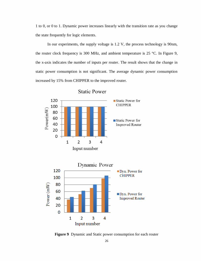
In our experiments, the supply voltage is 1.2 V, the process technology is 90nm,
the router clock frequency is 300 MHz, and ambient temperature is 25 °C. In Figure 9,
the x-axis indicates the number of inputs per router. The result shows that the change in
static power consumption is not significant. The average dynamic power consumption
increased by 15% from CHIPPER to the improved router.
Figure 9 Dynamic and Static power consumption for each router
27
IV.E Latency
Figure 10 Flit average latency
Figure 11 The latency information for each router
0
2
4
6
8
10
12
14
16
18
20
0.1 0.2 0.3 0.4
Lat
ency
(cy
cle)
Injection Rate
Average Latency
Dual-ejection CHIPPER
Optimized Router
0
20
40
60
80
100
120
140
160
180
0.1 0.1 0.2 0.2 0.3 0.3 0.4 0.4
Lat
ency
(cy
cle)
Injection Rate
Dual-ejection CHIPPER
Improved Router
Max Latency 3rd Quartile Median 1st Quatile Min Latency

28
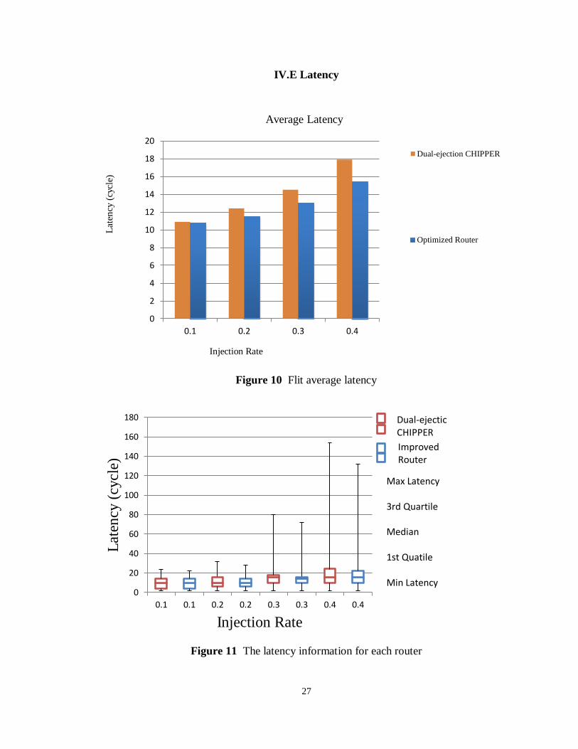
Latency is a measure of time delay experienced in the system. In the NoC system, time
latency is defined as the time from the flit starts to require the local input until the flit
reaches the destination node. Figure 10 shows the average latency for injected flits. The
impact of changing the permutation structure is illustrated when the injection rate is high.
Up to 16.2% of average latency has been decreased when the injection rate is 0.4 flits per
cycle per node. Figure 11 shows the latency distribution information. It depicts the
latency through their quartiles. The improved router reduces the variance in the latency as
well as the maximum (i.e., worst-case) delay observed in our experiments.

29
CHAPTER V
SUMMARY AND FUTURE WORK
This thesis presents an improved bufferless router architecture based on the CHIPPER
design. The improved bufferless router implements a new permutation component that
balances the pipeline stages and reduces the average latency of flits. The design operates
at the same clock frequency as the Dual-ejection CHIPPER. By adding the Final Chance
module and modifying the rules for permutation, the deflection rate has been reduced,
and the result shows the average latency was reduced effectively. Since CHIPPER saves
area and power significantly when compared to buffered routers, the increased area and
power in the improved router still compare favorably to buffered routers. Thus, the
improved bufferless router is an effective compromise between a conventional buffered
router and CHIPPER.
The future work in this area involves on two enhancements. One is that we plan to
implement our improved bufferless router in more topologies and test their performance
with multiple benchmarks. The other enhancement we plan is to measure the maximum
clock frequency with advanced CMOS manufacturing process and make sure our
balanced design can work on different CMOS manufacturing processes as well.
30
REFERENCES
[1] L. Benini and G. De Micheli, "Networks on chips: A new SoC paradigm,"
Computer, vol. 35, pp. 70-78, 2002.
[2] S. Pasricha and N. Dutt, On-chip communication architectures: system on chip
interconnect: Morgan Kaufmann, 2010.
[3] W. J. Dally and B. Towles, "Route packets, not wires: On-chip interconnection
networks," in Design Automation Conference, 2001. Proceedings, 2001, pp. 684-
689.
[4] W. J. Dally and B. P. Towles, Principles and practices of interconnection
networks: Morgan Kaufmann, 2004.
[5] T. Bjerregaard and J. Sparso, "Virtual channel designs for guaranteeing
bandwidth in asynchronous network-on-chip," in Norchip Conference, 2004.
Proceedings, 2004, pp. 269-272.
[6] N. Kavaldjiev, G. J. Smit, P. G. Jansen, and P. T. Wolkotte, "A Virtual Channel
Network-on-Chip for GT and BE traffic," in Emerging VLSI Technologies and
Architectures, 2006. IEEE Computer Society Annual Symposium on, 2006, p. 6
pp.
[7] A. Mello, L. Tedesco, N. Calazans, and F. Moraes, "Virtual channels in networks
on chip: implementation and evaluation on hermes NoC," in Proceedings of the
18th annual symposium on Integrated circuits and system design, 2005, pp. 178-
183.
[8] W. J. Dally, "Virtual-channel flow control," Parallel and Distributed Systems,
IEEE Transactions on, vol. 3, pp. 194-205, 1992.
[9] K. Sankaralingam, R. Nagarajan, R. McDonald, R. Desikan, S. Drolia, M.
Govindan, et al., "Distributed microarchitectural protocols in the TRIPS prototype
processor," in Microarchitecture, 2006. MICRO-39. 39th Annual IEEE/ACM
International Symposium on, 2006, pp. 480-491.
[10] M. B. Taylor, J. Kim, J. Miller, D. Wentzlaff, F. Ghodrat, B. Greenwald, et al.,
"The Raw microprocessor: A computational fabric for software circuits and
general-purpose programs," Micro, IEEE, vol. 22, pp. 25-35, 2002.
[11] M. Coenen, S. Murali, A. Radulescu, K. Goossens, and G. De Micheli, "A buffer-
sizing algorithm for networks on chip using TDMA and credit-based end-to-end
flow control," in Hardware/Software Codesign and System Synthesis, 2006.

31
CODES+ ISSS'06. Proceedings of the 4th International Conference, 2006, pp.
130-135.
[12] G. Nychis, C. Fallin, T. Moscibroda, and O. Mutlu, "Next generation on-chip
networks: what kind of congestion control do we need?," in Proceedings of the
9th ACM SIGCOMM Workshop on Hot Topics in Networks, 2010, p. 12.
[13] M. Palesi, R. Holsmark, S. Kumar, and V. Catania, "A methodology for design of
application specific deadlock-free routing algorithms for NoC systems," in
Proceedings of the 4th international conference on Hardware/software codesign
and system synthesis, 2006, pp. 142-147.
[14] T. Moscibroda and O. Mutlu, "A case for bufferless routing in on-chip networks,"
in ACM SIGARCH Computer Architecture News, 2009, pp. 196-207.
[15] C. Fallin, C. Craik, and O. Mutlu, "CHIPPER: A low-complexity bufferless
deflection router," in High Performance Computer Architecture (HPCA), 2011
IEEE 17th International Symposium on, 2011, pp. 144-155.
[16] C. Fallin, G. Nazario, X. Yu, K. Chang, R. Ausavarungnirun, and O. Mutlu,
"MinBD: Minimally-buffered deflection routing for energy-efficient
interconnect," in Networks on Chip (NoCS), 2012 Sixth IEEE/ACM International
Symposium on, 2012, pp. 1-10.
[17] G. Michelogiannakis, D. Sanchez, W. J. Dally, and C. Kozyrakis, "Evaluating
bufferless flow control for on-chip networks," in Proceedings of the 2010 Fourth
ACM/IEEE International Symposium on Networks-on-Chip, 2010, pp. 9-16.
[18] Z. Salcic and A. Smailagic, Digital systems design and prototyping: using field
programmable logic and hardware description languages: Kluwer Academic
Pub, 2000.
[19] R. Marculescu and P. Bogdan, "The chip is the network: Toward a science of
network-on-chip design," Foundations and Trends® in Electronic Design
Automation, vol. 2, pp. 371-461, 2007.
[20] P. Magarshack and P. G. Paulin, "System-on-chip beyond the nanometer wall," in
Design Automation Conference, 2003. Proceedings, 2003, pp. 419-424.
[21] M. Horowitz and W. Dally, "How scaling will change processor architecture," in
Solid-State Circuits Conference, 2004. Digest of Technical Papers. ISSCC. 2004
IEEE International, 2004, pp. 132-133.
[22] T. Bjerregaard and S. Mahadevan, "A survey of research and practices of
network-on-chip," ACM Computing Surveys (CSUR), vol. 38, p. 1, 2006.

32
[23] R. Mullins, A. West, and S. Moore, "Low-latency virtual-channel routers for on-
chip networks," in ACM SIGARCH Computer Architecture News, 2004, p. 188.
[24] J. Kwa and T. M. Aamodt, "Small virtual channel routers on FPGAs through
block RAM sharing," in Field-Programmable Technology (FPT), 2012
International Conference on, 2012, pp. 71-79.
[25] P. Baran, "On distributed communications networks," Communications Systems,
IEEE Transactions on, vol. 12, pp. 1-9, 1964.
[26] I. Kuon and J. Rose, "Measuring the gap between FPGAs and ASICs," Computer-
Aided Design of Integrated Circuits and Systems, IEEE Transactions on, vol. 26,
pp. 203-215, 2007.
[27] Altera, "Altera DE2-115 User Manual."
[28] I. Altera Quartus, "9.0 Software Manuals," Altera Inc., San Jose, CA (www.
altera. com), 2009.
[29] "ModelSim - Advanced Simulation and Debugging. http : //model.com."
[30] Y. Lu, J. McCanny, and S. Sezer, "Generic low-latency NoC router architecture
for FPGA computing systems," in Field Programmable Logic and Applications
(FPL), 2011 International Conference on, 2011, pp. 82-89.
[31] T. R. Henderson, M. Lacage, G. F. Riley, C. Dowell, and J. Kopena, "Network
simulations with the ns-3 simulator," SIGCOMM demonstration, 2008.

33
APPENDIX
Implement improved bufferless router using VHDL
library IEEE;
use IEEE.STD_LOGIC_1164.ALL;
use IEEE.STD_LOGIC_ARITH.ALL;
use IEEE.STD_LOGIC_UNSIGNED.ALL;
use work.pkg_IBR_NOC.all;
----------------------------------------------------The computation stage-----------------------------------------------
---
---------The functions are inject/eject flits and compute the desired direction of flits------------
entity first_stage is
port(
local_address : in data_address_type;
data_in_address : in data_address_array(DATA_DIR_NUM-1 downto 0);
ID_in : in ID_array(DATA_DIR_NUM-1 downto 0);
inject_data_address : in data_address_type;
inject_ID : in ID_type;
inject_port_req: in std_logic;
data_out_address : out data_address_array(DATA_DIR_NUM-1 downto 0);
data_ejection : out ID_array(EJECTION_PORT_NUM-1 downto 0);
ID_out : out ID_array(DATA_DIR_NUM-1 downto 0);
data_direction : out data_direction_array(DATA_DIR_NUM-1 downto 0);
req : buffer std_logic:='0';
clk : in std_logic;
reset : in std_logic
);
end first_stage;
architecture behavioral of first_stage is
signal temp_data_address_1, temp_data_address_2, temp_data_address_3 :
data_address_array(DATA_DIR_NUM-1 downto 0);
signal temp_ID_1, temp_ID_2, temp_ID_3 : ID_array(DATA_DIR_NUM-1 downto 0);
begin
eject_port : process(clk,reset)
begin
-----------------Initialization------------------
if reset='1' then
temp_ID_1 <= (others =>(others => '0'));
temp_data_address_1 <= (others =>(others => '0'));
data_ejection(1) <= (OTHERS=>'0');
----------------First ejection port-----------------

34
elsif clk'event and clk ='1' then
if data_in_address(3) = local_address and ID_in(3)/= empty then
data_ejection(1) <= ID_in(3);
temp_data_address_1(3) <= (others => '0');
temp_ID_1(3) <= (others => '0');
temp_data_address_1(2 downto 0) <= data_in_address(2 downto 0);
temp_ID_1(2 downto 0) <= ID_in(2 downto 0);
elsif data_in_address(2) = local_address and ID_in(2)/= empty then
data_ejection(1) <= ID_in(2);
temp_data_address_1(2) <= (others => '0');
temp_ID_1(2) <= (others => '0');
temp_data_address_1(3)<= data_in_address(3);
temp_ID_1(3) <= ID_in(3);
temp_data_address_1(1)<= data_in_address(1);
temp_ID_1(1) <= ID_in(1);
temp_data_address_1(0)<= data_in_address(0);
temp_ID_1(0) <= ID_in(0);
elsif data_in_address(1) = local_address and ID_in(1)/= empty then
data_ejection(1) <= ID_in(1);
temp_data_address_1(1) <= (others => '0');
temp_ID_1(1) <= (others => '0');
temp_data_address_1(3) <= data_in_address(3);
temp_ID_1(3) <= ID_in(3);
temp_data_address_1(2)<= data_in_address(2);
temp_ID_1(2) <= ID_in(2);
temp_data_address_1(0)<= data_in_address(0);
temp_ID_1(0) <= ID_in(0);
elsif data_in_address(0) = local_address and ID_in(0)/= empty then
data_ejection(1) <= ID_in(0);
temp_data_address_1(0) <= (others => '0');
temp_ID_1(0) <= (others => '0');
temp_data_address_1(3 downto 1) <= data_in_address(3 downto 1);
temp_ID_1(3 downto 1) <= ID_in(3 downto 1);
else
temp_ID_1 <= ID_in;
temp_data_address_1 <= data_in_address;
end if;
end if;
end process;
--------------------Second ejection port-----------------
dual_ejection : process(reset, temp_ID_1, temp_data_address_1)
begin

35
if reset = '1' then data_ejection(0)<= (OTHERS=>'0');
elsif temp_data_address_1(2) = local_address and ID_in(2)/= empty then
data_ejection(0) <= temp_ID_1(2);
temp_data_address_2(2) <= (others => '0');
temp_ID_2(2) <= (others => '0');
temp_data_address_2(3)<= temp_data_address_1(3);
temp_ID_2(3) <= temp_ID_1(3);
temp_data_address_2(1)<= temp_data_address_1(1);
temp_ID_2(1) <= temp_ID_1(1);
temp_data_address_2(0)<= temp_data_address_1(0);
temp_ID_2(0) <= temp_ID_1(0);
elsif temp_data_address_1(1) = local_address and ID_in(1)/= empty then
data_ejection(0) <= temp_ID_1(1);
temp_data_address_2(1) <= (others => '0');
temp_ID_2(1) <= (others => '0');
temp_data_address_2(3) <= temp_data_address_1(3);
temp_ID_2(3) <= temp_ID_1(3);
temp_data_address_2(2)<= temp_data_address_1(2);
temp_ID_2(2) <= temp_ID_1(2);
temp_data_address_2(0)<= temp_data_address_1(0);
temp_ID_2(0) <= temp_ID_1(0);
elsif temp_data_address_1(0) = local_address and ID_in(0)/= empty then
data_ejection(0) <= temp_ID_1(0);
temp_data_address_2(0) <= (others => '0');
temp_ID_2(0) <= (others => '0');
temp_data_address_2(3 downto 1) <= temp_data_address_1(3 downto 1);
temp_ID_2(3 downto 1) <= temp_ID_1(3 downto 1);
else
temp_ID_2 <= temp_ID_1;
temp_data_address_2 <= temp_data_address_1;
end if;
end process;
------------------------Injection port----------------------
injection : process(temp_ID_2, temp_data_address_2,req)
begin
if req = '0' then
if inject_port_req = '1' then
if temp_ID_2(3) = empty then
temp_data_address_3(3) <= inject_data_address;
temp_data_address_3(2 downto 0) <= temp_data_address_2(2 downto 0);
temp_ID_3(3) <= inject_ID;
36
temp_ID_3(2 downto 0) <= temp_ID_2(2 downto 0);
req <= '1';
elsif temp_ID_2(2) = empty then
temp_data_address_3(3) <= temp_data_address_2(3);
temp_data_address_3(2) <= inject_data_address;
temp_data_address_3(1 downto 0) <= temp_data_address_2(1 downto 0);
temp_ID_3(3) <= temp_ID_2(3);
temp_ID_3(2) <= inject_ID;
temp_ID_3(1 downto 0) <= temp_ID_2(1 downto 0);
req <= '1';
elsif temp_ID_2(1) = empty then
temp_data_address_3(3) <= temp_data_address_2(3);
temp_data_address_3(2) <= temp_data_address_2(2);
temp_data_address_3(1) <= inject_data_address;
temp_data_address_3(0) <= temp_data_address_2(0);
temp_ID_3(3) <= temp_ID_2(3);
temp_ID_3(2) <= temp_ID_2(2);
temp_ID_3(1) <= inject_ID;
temp_ID_3(0) <= temp_ID_2(0);
req <= '1';
elsif temp_ID_2(0) = empty then
temp_data_address_3(3 downto 1) <= temp_data_address_2(3 downto 1);
temp_data_address_3(0) <= inject_data_address;
temp_ID_3(3 downto 1) <= temp_ID_2(3 downto 1);
temp_ID_3(0) <= inject_ID;
req <= '1';
else
temp_data_address_3(3 downto 0) <= temp_data_address_2(3 downto 0);
temp_ID_3(3 downto 0) <= temp_ID_2(3 downto 0);
end if;
else
temp_data_address_3(3 downto 0) <= temp_data_address_2(3 downto 0);
temp_ID_3(3 downto 0) <= temp_ID_2(3 downto 0);
end if;
else req <= '0';
end if;
end process;
-----------------Compute the desired direction----------------
direction : process(temp_ID_3, temp_data_address_3)
begin
if temp_ID_3(3)=empty then data_direction(3) <= NONE;

37
elsif temp_data_address_3(3)(ADDRESS_SIZE-1 downto MESH_COLUMN_BI) >
local_address(ADDRESS_SIZE-1 downto MESH_COLUMN_BI) then
data_direction(3) <= SOUTH;
elsif temp_data_address_3(3)(ADDRESS_SIZE-1 downto MESH_COLUMN_BI) <
local_address(ADDRESS_SIZE-1 downto MESH_COLUMN_BI) then
data_direction(3) <= NORTH;
elsif temp_data_address_3(3)(MESH_COLUMN_BI-1 downto 0) >
local_address(MESH_COLUMN_BI-1 downto 0) then
data_direction(3) <= EAST;
elsif temp_data_address_3(3)(MESH_COLUMN_BI-1 downto 0) <
local_address(MESH_COLUMN_BI-1 downto 0) then
data_direction(3) <= WEST;
else
data_direction(3) <= WEST;
end if;
if temp_ID_3(2)=empty then data_direction(2) <= NONE;
elsif temp_data_address_3(2)(MESH_COLUMN_BI-1 downto 0) >
local_address(MESH_COLUMN_BI-1 downto 0) then
data_direction(2) <= EAST;
elsif temp_data_address_3(2)(MESH_COLUMN_BI-1 downto 0) <
local_address(MESH_COLUMN_BI-1 downto 0) then
data_direction(2) <= WEST;
elsif temp_data_address_3(2)(ADDRESS_SIZE-1 downto MESH_COLUMN_BI) >
local_address(ADDRESS_SIZE-1 downto MESH_COLUMN_BI) then
data_direction(2) <= SOUTH;
elsif temp_data_address_3(2)(ADDRESS_SIZE-1 downto MESH_COLUMN_BI) <
local_address(ADDRESS_SIZE-1 downto MESH_COLUMN_BI) then
data_direction(2) <= NORTH;
else
data_direction(2) <= NORTH;
end if;
if temp_ID_3(1)=empty then data_direction(1) <= NONE;
elsif temp_data_address_3(1)(ADDRESS_SIZE-1 downto MESH_COLUMN_BI) >
local_address(ADDRESS_SIZE-1 downto MESH_COLUMN_BI) then
data_direction(1) <= SOUTH;
elsif temp_data_address_3(1)(ADDRESS_SIZE-1 downto MESH_COLUMN_BI) <
local_address(ADDRESS_SIZE-1 downto MESH_COLUMN_BI) then
data_direction(1) <= NORTH;
elsif temp_data_address_3(1)(MESH_COLUMN_BI-1 downto 0) >
local_address(MESH_COLUMN_BI-1 downto 0) then
data_direction(1) <= EAST;
elsif temp_data_address_3(1)(MESH_COLUMN_BI-1 downto 0) <
local_address(MESH_COLUMN_BI-1 downto 0) then
data_direction(1) <= WEST;
else

38
data_direction(1) <= WEST;
end if;
if temp_ID_3(0)=empty then data_direction(0) <= NONE;
elsif temp_data_address_3(0)(MESH_COLUMN_BI-1 downto 0) >
local_address(MESH_COLUMN_BI-1 downto 0) then
data_direction(0) <= EAST;
elsif temp_data_address_3(0)(MESH_COLUMN_BI-1 downto 0) <
local_address(MESH_COLUMN_BI-1 downto 0) then
data_direction(0) <= WEST;
elsif temp_data_address_3(0)(ADDRESS_SIZE-1 downto MESH_COLUMN_BI) >
local_address(ADDRESS_SIZE-1 downto MESH_COLUMN_BI) then
data_direction(0) <= SOUTH;
elsif temp_data_address_3(0)(ADDRESS_SIZE-1 downto MESH_COLUMN_BI) <
local_address(ADDRESS_SIZE-1 downto MESH_COLUMN_BI) then
data_direction(0) <= NORTH;
else
data_direction(0) <= NORTH;
end if;
end process;
display_out :process(temp_data_address_3,temp_ID_3)
begin
data_out_address <= temp_data_address_3;
ID_out <= temp_ID_3;
end process;
end behavioral;
---------------------------------------------------------------------------------------------------------------------------------
---------------------------------------------------The permutation stage-------------------------------------------------
library IEEE;
use IEEE.STD_LOGIC_1164.ALL;
use IEEE.STD_LOGIC_ARITH.ALL;
use IEEE.STD_LOGIC_UNSIGNED.ALL;
use work.pkg_IBR_NOC.all;
entity deflection is
port(
data_in_address : in data_address_array(DATA_DIR_NUM-1 downto 0);
data_direction_in : in data_direction_array(DATA_DIR_NUM-1 downto 0);
ID_in : in ID_array(DATA_DIR_NUM-1 downto 0);
data_out_address: out data_address_array(DATA_DIR_NUM-1 downto 0);
ID_out : out ID_array(DATA_DIR_NUM-1 downto 0);
data_direction_out : out data_direction_array(DATA_DIR_NUM-1 downto 0);

39
clk : in std_logic;
reset : in std_logic
);
end deflection;
architecture behavioral of deflection is
signal temp_data_direction_2, temp_data_direction_3, temp_data_direction_4, temp_data_direction_5 :
data_direction_array(DATA_DIR_NUM-1 downto 0);
signal temp_data_address_2, temp_data_address_3, temp_data_address_4, temp_data_address_5 : data_address_array(DATA_DIR_NUM-1 downto 0);
signal temp_ID_2, temp_ID_3, temp_ID_4, temp_ID_5 : ID_array(DATA_DIR_NUM-1 downto 0);
begin
stage_1 : process(clk,reset)
begin
--------------Initialization--------------------
if reset = '1' then
temp_data_address_2 <= (others =>(others => '0'));
temp_data_direction_2 <= (others =>(others => '0'));
temp_ID_2 <= (others =>(others => '0'));
--------------Top left arbiter------------------
elsif clk'event and clk ='1' then
if (data_direction_in(3)=EAST or data_direction_in(3)=SOUTH) or
(data_direction_in(2)=WEST or data_direction_in(2)=NORTH)
then
temp_data_direction_2(3 downto 2)<=data_direction_in(3 downto 2);
temp_data_address_2(3 downto 2) <= data_in_address(3 downto 2);
temp_ID_2(3 downto 2) <= ID_in(3 downto 2);
else
temp_data_direction_2(3)<=data_direction_in(2);
temp_data_direction_2(2)<=data_direction_in(3);
temp_data_address_2(3)<=data_in_address(2);
temp_data_address_2(2)<=data_in_address(3);
temp_ID_2(3)<=ID_in(2);
temp_ID_2(2)<=ID_in(3);
end if;
--------------Bottom left arbiter------------------
if (data_direction_in(1)=EAST or data_direction_in(1)=SOUTH) or
(data_direction_in(0)=WEST or data_direction_in(0)=NORTH)
then
temp_data_direction_2(1 downto 0)<=data_direction_in(1 downto 0);
temp_data_address_2(1 downto 0)<=data_in_address(1 downto 0);

40
temp_ID_2(1 downto 0)<=ID_in(1 downto 0);
else
temp_data_direction_2(1)<=data_direction_in(0);
temp_data_direction_2(0)<=data_direction_in(1);
temp_data_address_2(1)<=data_in_address(0);
temp_data_address_2(0)<=data_in_address(1);
temp_ID_2(1)<=ID_in(0);
temp_ID_2(0)<=ID_in(1);
end if;
end if;
end process;
--------------Middle swap------------------
stage_swap: process(temp_data_direction_2,temp_data_address_2, temp_ID_2)
begin
temp_data_direction_3(3) <= temp_data_direction_2(3);
temp_data_direction_3(2) <= temp_data_direction_2(1);
temp_data_direction_3(1) <= temp_data_direction_2(2);
temp_data_direction_3(0) <= temp_data_direction_2(0);
temp_data_address_3(3) <= temp_data_address_2(3);
temp_data_address_3(2) <= temp_data_address_2(1);
temp_data_address_3(1) <= temp_data_address_2(2);
temp_data_address_3(0) <= temp_data_address_2(0);
temp_ID_3(3) <= temp_ID_2(3);
temp_ID_3(2) <= temp_ID_2(1);
temp_ID_3(1) <= temp_ID_2(2);
temp_ID_3(0) <= temp_ID_2(0);
end process;
--------------Top right arbiter------------------
stage_2: process(temp_data_direction_3,temp_data_address_3, temp_ID_3)
begin
if (temp_data_direction_3(3)=EAST or temp_data_direction_3(2)=SOUTH)
then
temp_data_direction_4(3 downto 2) <= temp_data_direction_3(3 downto 2);
temp_data_address_4(3 downto 2) <= temp_data_address_3(3 downto 2);
temp_ID_4(3 downto 2) <= temp_ID_3(3 downto 2);
else
temp_data_direction_4(3)<=temp_data_direction_3(2);
temp_data_direction_4(2)<=temp_data_direction_3(3);
temp_data_address_4(3)<=temp_data_address_3(2);
temp_data_address_4(2)<=temp_data_address_3(3);
temp_ID_4(3)<=temp_ID_3(2);
temp_ID_4(2)<=temp_ID_3(3);
41
end if;
--------------Bottom right arbiter------------------
if (temp_data_direction_3(1)=WEST or temp_data_direction_3(0)=NORTH)
then
temp_data_direction_4(1 downto 0) <= temp_data_direction_3(1 downto 0);
temp_data_address_4(1 downto 0) <= temp_data_address_3(1 downto 0);
temp_ID_4(1 downto 0) <= temp_ID_3(1 downto 0);
else
temp_data_direction_4(1)<=temp_data_direction_3(0);
temp_data_direction_4(0)<=temp_data_direction_3(1);
temp_data_address_4(1)<=temp_data_address_3(0);
temp_data_address_4(0)<=temp_data_address_3(1);
temp_ID_4(1)<=temp_ID_3(0);
temp_ID_4(0)<=temp_ID_3(1);
end if;
end process;
--------------Final chance component------------------
stage_3 : process(temp_data_direction_4,temp_data_address_4,temp_ID_4)
begin
if temp_data_direction_4(3) /= EAST
then
if temp_data_direction_4(1) /= WEST and temp_data_direction_4(3) /= NONE
and temp_data_direction_4(1) /= NONE then
temp_data_direction_5(3)<=temp_data_direction_4(1);
temp_data_direction_5(2)<=temp_data_direction_4(2);
temp_data_direction_5(1)<=temp_data_direction_4(3);
temp_data_direction_5(0)<=temp_data_direction_4(0);
temp_data_address_5(3)<=temp_data_address_4(1);
temp_data_address_5(2)<=temp_data_address_4(2);
temp_data_address_5(1)<=temp_data_address_4(3);
temp_data_address_5(0)<=temp_data_address_4(0);
temp_ID_5(3)<=temp_ID_4(1);
temp_ID_5(2)<=temp_ID_4(2);
temp_ID_5(1)<=temp_ID_4(3);
temp_ID_5(0)<=temp_ID_4(0);
elsif temp_data_direction_4(0) /= NORTH and temp_data_direction_4(3) /=
NONE and temp_data_direction_4(0) /= NONE then
temp_data_direction_5(3)<=temp_data_direction_4(0);
temp_data_direction_5(2)<=temp_data_direction_4(2);
temp_data_direction_5(1)<=temp_data_direction_4(1);
temp_data_direction_5(0)<=temp_data_direction_4(3);

42
temp_data_address_5(3)<=temp_data_address_4(0);
temp_data_address_5(2)<=temp_data_address_4(2);
temp_data_address_5(1)<=temp_data_address_4(1);
temp_data_address_5(0)<=temp_data_address_4(3);
temp_ID_5(3)<=temp_ID_4(0);
temp_ID_5(2)<=temp_ID_4(2);
temp_ID_5(1)<=temp_ID_4(1);
temp_ID_5(0)<=temp_ID_4(3);
else
temp_data_direction_5<=temp_data_direction_4;
temp_data_address_5<=temp_data_address_4;
temp_ID_5<=temp_ID_4;
end if;
elsif temp_data_direction_4(2) /= SOUTH then
if temp_data_direction_4(0) /= NORTH and temp_data_direction_4(2) /=
NONE and temp_data_direction_4(0) /= NONE then
temp_data_direction_5(3)<=temp_data_direction_4(3);
temp_data_direction_5(2)<=temp_data_direction_4(0);
temp_data_direction_5(1)<=temp_data_direction_4(1);
temp_data_direction_5(0)<=temp_data_direction_4(2);
temp_data_address_5(3)<=temp_data_address_4(3);
temp_data_address_5(2)<=temp_data_address_4(0);
temp_data_address_5(1)<=temp_data_address_4(1);
temp_data_address_5(0)<=temp_data_address_4(2);
temp_ID_5(3)<=temp_ID_4(3);
temp_ID_5(2)<=temp_ID_4(0);
temp_ID_5(1)<=temp_ID_4(1);
temp_ID_5(0)<=temp_ID_4(2);
elsif temp_data_direction_4(1) /= WEST and temp_data_direction_4(2) /= NONE and temp_data_direction_4(1) /= NONE then
temp_data_direction_5(3)<=temp_data_direction_4(3);
temp_data_direction_5(2)<=temp_data_direction_4(1);
temp_data_direction_5(1)<=temp_data_direction_4(2);
temp_data_direction_5(0)<=temp_data_direction_4(0);
temp_data_address_5(3)<=temp_data_address_4(3);
temp_data_address_5(2)<=temp_data_address_4(1);
temp_data_address_5(1)<=temp_data_address_4(2);
temp_data_address_5(0)<=temp_data_address_4(0);
temp_ID_5(3)<=temp_ID_4(3);
temp_ID_5(2)<=temp_ID_4(1);
temp_ID_5(1)<=temp_ID_4(2);
temp_ID_5(0)<=temp_ID_4(0);

43
else
temp_data_direction_5<=temp_data_direction_4;
temp_data_address_5<=temp_data_address_4;
temp_ID_5<=temp_ID_4;
end if;
else
temp_data_direction_5<=temp_data_direction_4;
temp_data_address_5<=temp_data_address_4;
temp_ID_5<=temp_ID_4;
end if;
end process;
data_out_address<=temp_data_address_5;
ID_out<=temp_ID_5;
end behavioral;


![Load Balanced Routing Mechanisms for Mobile Ad Hoc Networks · Load-Aware Routing (CLAR) [7] protocol is an on-de-mand routing protocol. In CLAR, traffic load at a node is considered](https://cdn.vdocuments.us/doc/165x107/60240704fcf69450005af8e7/load-balanced-routing-mechanisms-for-mobile-ad-hoc-networks-load-aware-routing-clar.jpg)
