Impact of electrode roughness on metal-insulator-metal tunnel diodes withatomic layer deposited Al2O3 tunnel barriers
Nasir Alimardani, E. William Cowell III, John F. Wager, and John F. Conley, Jr.a)
School of EECS, Oregon State University, 1148 Kelley Engineering Center, Corvallis, Oregon 97331
David R. EvansSharp Laboratories of America, Inc., Camas, Washington 98607
Matthew Chin, Stephen J. Kilpatrick, and Madan DubeyU.S. Army Research Laboratory, Adelphi, Maryland 20783
(Received 16 August 2011; accepted 12 October 2011; published 3 November 2011)
Metal-insulator-metal (MIM) tunnel diodes on a variety of high and low work function metals with
various levels of root-mean-square roughness are fabricated using high quality atomic layer
deposited Al2O3 as the insulating tunnel barrier. It is found that electrode surface roughness can
dominate the current versus voltage characteristics of MIM diodes, even overwhelming the impact
of metal work function. Devices with smoother bottom electrodes are found to produce current
versus voltage behavior with higher asymmetry and better agreement with Fowler-Nordheim
tunneling theory, as well as a greater percentage of functioning devices. VC 2012 American VacuumSociety. [DOI: 10.1116/1.3658380]
I. INTRODUCTION
Metal-insulator-metal (MIM)-based tunneling devices
with very thin insulator layers compared to those of MIM
capacitors have been proposed for a variety of applications,
including hot electron transistors,1,2 infrared (IR) detec-
tors,3,4 liquid-crystal display backplanes,5 optical rectennas
for IR energy harvesting,6 and macroelectronics.7 Despite
investigation by many groups over many decades, progress
toward the commercialization of MIM-based electronics has
been hindered by the lack of a manufacturable process for
the fabrication of high-quality MIM diodes. The operation of
a MIM diode is based on quantum mechanical tunneling
through a thin insulating film positioned between two metal
electrodes.8,9 The tunneling probability depends exponen-
tially on the thickness of the insulator/insulator electric field;
thus, the performance of a MIM tunnel diode should depend
strongly on the atomic scale roughness and the uniformity of
the electrode-insulator interfaces.9–11 In fact, Miller et al.12
have theoretically predicted that the interfacial roughness
should affect the tunneling current in tunnel junctions. Inat-
tention to the electrode roughness, along with the lack of a
high-quality deposited oxide, appears to have slowed the de-
velopment of this technology. Most experimental work to
date on MIM diodes has focused on the use of thin native
dielectrics produced by oxidation or nitridation of the under-
lying polycrystalline metal electrode.1–4,13–17
Basic studies on electrode and interface roughness and
their correlation with the tunneling current will be very im-
portant for the advancement of MIM technology. Recently,
we demonstrated that sputter deposition of the amorphous
metal ZrCuAlNi can be used to produce an ultrasmooth elec-
trode (�0.3 nm root-mean-square (RMS) roughness).18
Although the use of ZrCuAlNi as a bottom electrode in con-
junction with high-quality Al2O3 deposited via ALD allowed
for the reproducible fabrication of MIM tunnel diodes, we
were unable to make any functioning devices on very rough
Al bottom electrodes. Although it was hypothesized that the
reason for the good electrical characteristics on ZrCuAlNi,
as opposed to the complete lack of functioning devices on
Al, was due to the large difference in roughness, our previ-
ous work did not discuss the case of intermediate electrode
roughness, in which the electrode roughness is not great
enough to destroy all devices but is still large enough so that
it might impact the electrical characteristics of functioning
devices.
In the work presented herein, we compare MIM tunnel
diode performance on low work function (ZrCuAlNi and Al)
and high work function (Ir and two types of Pt) bottom elec-
trode materials with various levels of RMS roughness.
Whereas previous MIM diode work has focused primarily
on native oxides, the use of atomic layer deposition (ALD)
allows for the deposition of the same high-quality Al2O3 in-
sulator on each of these bottom metal electrodes. We show
that roughness can overwhelm the impact of the metal work
function on the electrical characteristics of MIM diodes, in
fact reversing the expected trends based on metal work func-
tions. We also find that that the percentage yield of function-
ing devices tracks higher with decreasing roughness. Finally,
we find that even for nominally the same metal (Pt), the level
of roughness dominates the electrical characteristics and
yield.
II. EXPERIMENT
MIM diodes were fabricated on Si substrates capped with
100 nm of thermally grown SiO2. First, blanket films of Al,
Pt, Ir, or ZrCuAlNi were deposited as bottom electrodes. A
thin Ti adhesion layer was used for Pt and Ir. Al was
deposited via thermal evaporation, Ir was deposited via
electron-beam evaporation, and Pt was deposited using ei-
ther dc sputtering (Pt-1) or electron-beam evaporation (Pt-2).a)Electronic mail: [email protected]
01A113-1 J. Vac. Sci. Technol. A 30(1), Jan/Feb 2012 0734-2101/2012/30(1)/01A113/5/$30.00 VC 2012 American Vacuum Society 01A113-1
Author complimentary copy. Redistribution subject to AIP license or copyright, see http://jva.aip.org/jva/copyright.jsp
ZrCuAlNi was deposited via dc magnetron sputtering with
no intentional substrate heating using a 3 in. diameter, 0.25
in. thick vacuum arc-melted metal target (with an atomic
composition of Zr40Cu35Al15Ni10).18 Next, a thin (. 10 nm)
Al2O3 tunneling barrier was deposited via ALD using a Pico-
sun SUNALE R-150B ALD reactor by alternating pulses of
trimethlyaluminum (TMA) and de-ionized water at a tem-
perature of 300 �C. Finally, top electrodes were formed by
evaporating Al dots (�0.8 mm2) through a shadow mask.
Current density-electric field (J-n) characterization was
conducted using an Agilent 4156 C semiconductor parameter
analyzer with samples at room temperature in the dark. The
bottom electrode roughness (RMS and peak) was measured
via atomic force microscopy (AFM) using a Digital Instru-
ments 3 AFM with silicon-nitride tips. The work functions of
bottom electrodes were measured in air over an area of
approximately (1� 1) mm2 using a KP Technology SKP5050
scanning Kelvin probe with a 2 mm tip and calibrated against
a gold standard. The work functions of ZrCuAlNi and Al
were measured as approximately 4.8 eV and 4 eV, respec-
tively. The thickness of Al2O3 films on ZrCuAlNi bottom
electrodes was measured as 9.5 6 0.5 nm via TEM assess-
ment18 and confirmed with a spectroscopic ellipsometer (J.A.
Woollam Co. WVASE32) using a Cauchy model.
III. RESULTS AND DISCUSSION
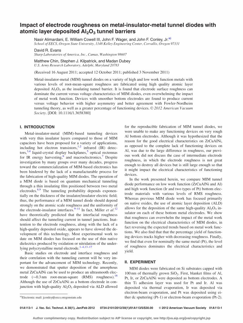
AFM micrographs, shown in Fig. 1, were used to establish
the RMS and peak roughness of as-deposited ZrCuAlNi, Pt-1,
Pt-2, and Ir bottom electrodes. The roughness values are aver-
aged from a minimum of three images each. In order to assess
any potential roughening as a result of the ALD thermal cycle
or interaction of the TMA precursor with the electrodes, addi-
tional AFM images were also taken after the deposition of a
10 nm Al2O3 layer (post-ALD). As summarized in Table I,
the AFM images reveal wide variation in both RMS average
roughness and peak roughness, with ZrCuAlNi having the
lowest roughness by a factor of 10. With the exception of Pt-
2, the RMS and peak roughness tend to scale together.
Following Al2O3 deposition, roughness values did not signifi-
cantly change for the smoothest as-deposited electrodes,
whereas the RMS roughness improved for the roughest as-
deposited electrode, Ir. In contrast, the Al electrodes were
found to roughen by about a factor of 5 after the Al2O3 depo-
sition. This increase in roughness is not due to the ALD
Al2O3 deposition itself; rather, it is a consequence of the low
melting point of Al and associated grain growth during the
ALD thermal cycle.
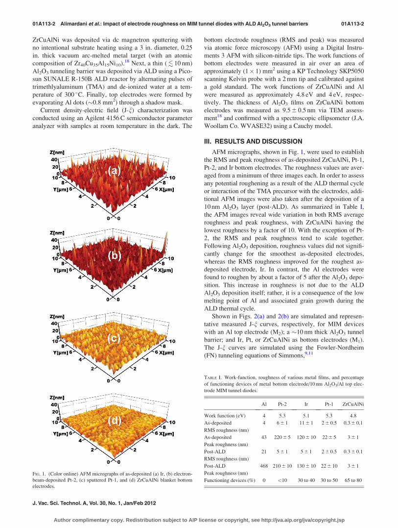
Shown in Figs. 2(a) and 2(b) are simulated and represen-
tative measured J-n curves, respectively, for MIM devices
with an Al top electrode (M2); a �10 nm thick Al2O3 tunnel
barrier; and Ir, Pt, or ZrCuAlNi as bottom electrodes (M1).
The J-n curves are simulated using the Fowler-Nordheim
(FN) tunneling equations of Simmons,9,11
FIG. 1. (Color online) AFM micrographs of as-deposited (a) Ir, (b) electron-
beam-deposited Pt-2, (c) sputtered Pt-1, and (d) ZrCuAlNi blanket bottom
electrodes.
TABLE I. Work-function, roughness of various metal films, and percentage
of functioning devices of metal bottom electrode/10 nm Al2O3/Al top elec-
trode MIM tunnel diodes.
Al Pt-2 Ir Pt-1 ZrCuAlNi
Work function (eV) 4 5.3 5.1 5.3 4.8
As-deposited 4 6 6 1 11 6 1 2 6 0.5 0.3 6 0.1
RMS roughness (nm)
As-deposited 43 220 6 5 120 6 10 22 6 5 3 6 1
Peak roughness (nm)
Post-ALD 21 5 6 1 5 6 1 2 6 0.5 0.3 6 0.1
RMS roughness (nm)
Post-ALD 468 210 6 10 130 6 10 22 6 10 3 6 1
Peak roughness (nm)
Functioning devices (%) 0 <10 30 to 40 30 to 50 65 to 80
01A113-2 Alimardani et al.: Impact of electrode roughness on MIM tunnel diodes with ALD Al2O3 tunnel barriers 01A113-2
J. Vac. Sci. Technol. A, Vol. 30, No. 1, Jan/Feb 2012
Author complimentary copy. Redistribution subject to AIP license or copyright, see http://jva.aip.org/jva/copyright.jsp

J ¼ 1:1q2
4ph
1
ub
V þ Dub
S
� �2
� exp�23p
ffiffiffiffiffiffiqmp
6hu3=2
b
S
V þ Dub
� �� �; (1)
where q is the electron charge, h is Plank’s constant, V is the
applied bias, ub is the barrier height of the electrode-
insulator interface from which electrons are tunneling, Dub
is the difference in barrier heights between the interfaces of
the insulator with the top and bottom electrodes, m is the
effective electron mass, and S is the tunnel barrier thickness.
Simulations were performed with MATLAB using an Al2O3
thickness of 10 nm, an electron affinity value of 2.58 eV for
ALD-Al2O3,19 and an electron effective mass of 0.79 of the
free electron mass.18 The only difference in the three simu-
lated curves is the work function of the bottom electrode
(M1), as given in Table I. In order to understand the J-ntrends of Fig. 2, it is necessary to consider MIM energy band
diagrams. The equilibrium band diagram of a symmetric
MIM tunnel device is shown in Fig. 3(a). The J-n character-
istic of a symmetric MIM device is expected to be symmet-
ric because the barrier to electron tunneling is the same in
either direction. The diodes investigated in this work have
asymmetric electrodes. The equilibrium band diagram of an
asymmetric MIM tunnel diode is shown in Fig. 3(b). ub1 and
ub2 indicate the barrier heights of the bottom electrode metal
M1 (Ir, Pt, or ZrCuAlNi) and the smaller work function top
gate electrode metal M2 (Al), respectively. Also shown are
band diagrams of the asymmetric diode at the onset of FN
tunneling for positive [Fig. 3(c)] and negative [Fig. 3(d)]
bias applied to M2 (assuming that M1 is grounded).
Considering first the application of a sufficiently large
positive bias to electrode M2, FN tunnel emission occurs
from the bottom electrode (M1; Ir, Pt, or ZrCuAlNi), with
different barrier heights as indicated in the energy band dia-
gram presented in the inset of Fig. 2(a). Note that the sketch
is for the applied bias in which tunnel emission from elec-
trode M1 transitions from direct tunneling (across the entire
insulator thickness) to FN tunneling (in which the tunnel
distance decreases with increasing bias, because of the now
triangular shape of the barrier). Because the insulator thick-
ness used (10 nm) is sufficient to suppress direct tunneling,
current conduction is dominated by FN tunneling. The prob-
ability of FN tunneling is exponentially dependent upon
the insulator thickness and the barrier height presented to the
tunneling electron [ub1 for positive biases, as shown in
the inset in Fig. 2(a)]. Thus, whereas the onset of FN tunnel-
ing for positive bias will be roughly the same for all bottom
electrodes (as it involves overcoming the same barrier
height, ub2, of the Al top electrode), the magnitude of the
FN tunneling current at larger positive fields (Vapp�ub2)
should be in the reverse order of increasing work function
(increasing ub1). Based on relative barrier heights, the cur-
rent density of the MIM diode with the ZrCuAlNi electrode
FIG. 2. (Color online) Plots of current density vs electric field (J-n) for MIM
diodes prepared with 10 nm Al2O3 and an Al top (M2) electrode. (a) Simu-
lated data for diodes with ZrCuAlNi, Ir, and Pt bottom (M1) electrodes (inset
compares band diagrams of diodes with different bottom electrodes under
positive bias; ZrCuAlNi is abbreviated as ZCAN). (b) Measured data for
devices fabricated using ZrCuAlNi, Ir, sputtered Pt-1, and electron-beam-
deposited Pt-2 bottom electrodes.
FIG. 3. (Color online) Equilibrium band diagrams of (a) symmetric and (b)
asymmetric tunnel diodes. ub1 and ub2 indicate the barrier height of the bot-
tom (high work function) and top (low work function) metal electrodes,
respectively. Energy band diagrams of an asymmetric tunnel diode under (c)
positive applied bias and (d) negative applied bias at the onset of FN
tunneling.
01A113-3 Alimardani et al.: Impact of electrode roughness on MIM tunnel diodes with ALD Al2O3 tunnel barriers 01A113-3
JVST A - Vacuum, Surfaces, and Films
Author complimentary copy. Redistribution subject to AIP license or copyright, see http://jva.aip.org/jva/copyright.jsp

(UZCAN¼ 4.8 eV) would be expected to be higher than that
of the device with the Pt electrode (UPt¼ 5.3 eV), whereas
the MIM diode with the Ir electrode (UIr¼ 5.1 eV) would be
intermediate.20 Although this trend is observed in the simu-
lation [Fig. 2(a)], it is clearly not the trend evidenced in
Fig. 2(b), based on the experimental data.
Assuming that the Al2O3 thickness for all devices is the
same and that conduction is dominated by FN tunneling, a
likely explanation for the unexpected trend shown in Fig. 2(b)
is associated with the relative roughness of the bottom elec-
trode. A rough bottom electrode could lead to electric field
nonuniformity across the insulator due to field enhancement
at sharp features, which would decrease the effective insulator
thickness. This field enhancement/decreased effective insula-
tor thickness would tend to lead to increased conduction. As
shown in Table I for the MIM structures measured in Fig.
2(b), Ir has the largest as-deposited RMS roughness (11 nm),
followed by e-beam-deposited Pt-2 (6 nm), sputtered Pt-1
(2 nm), and finally ZrCuAlNi (0.3 nm). As evident from Fig.
2(b), the positive polarity current density trend correlates with
the bottom electrode roughness, whereas the curve of the de-
vice with a ZrCuAlNi bottom electrode just matches with its
simulation.
The RMS roughness for both Ir and Pt-2 are comparable
to the overall dielectric thickness. Thus, it is not surprising
that the bottom electrode roughness overwhelms the
expected influence of the work function. Perhaps the clearest
indication of the impact of roughness can be seen by directly
comparing MIM tunnel diodes made using the same bottom
electrode (Pt) with two different levels of roughness. Despite
having the same nominal work function, the rougher e-beam
evaporated Pt-2 (RMS¼ 6 nm) device shows a higher posi-
tive bias current density than the smoother, dc sputtered Pt-1
(RMS¼ 2 nm) device [Fig. 2(b)].
Turning next to the application of a sufficiently large neg-ative bias to electrode M2, we see that electron tunnel emis-
sion now occurs from the top metal electrode (M2; Al), as
indicated in the energy band diagram in Fig. 3(d). The onset
of FN tunneling should not occur until larger negative vol-
tages for larger ub1, and the simulation in Fig. 2(a) shows
that the negative bias current density is expected to decrease
slightly with increasing M1 work function. As shown in the
measured data in Fig. 2(b), the devices made with ZrCuAlNi
as a bottom electrode once again match fairly well with the
simulation. Compared to the simulation, the voltage required
in order to achieve a given current density is reduced only
slightly for both the Pt and Ir electrode devices. Ir shows the
greatest deviation from the simulation, and the rougher Pt-2
once again deviates more than Pt-1.
The deviation between measured and simulated current
density is much less on the negative bias side than on the posi-
tive bias side (Fig. 2). Additional FN tunneling simulations
show that in an asymmetric MIM device, tunneling from the
higher work function side (in our case, positive bias tunnel
emission from M1) is more sensitive to changes in the tunnel
barrier (such as in thickness, electron effective mass, or elec-
tron affinity) than tunneling from the lower work function
side (in our case, negative bias tunnel emission from M2).
The data in Fig. 2 suggest that tunneling from the higher work
function side (which occurs under positive bias in our experi-
ments) is also more sensitive to roughness than tunneling
from the smaller work function side (which occurs under neg-
ative bias in our experiments). In addition, some smoothing of
the roughest electrodes is observed after ALD (Table I).
Whereas the roughness values did not change significantly for
ZrCuAlNi and Pt-1, the smoothest as-deposited electrodes,
the RMS roughness improved significantly for Ir (from 11 nm
to 5 nm) and slightly for Pt-2 (from 6 nm to 5 nm).
The desired J-n characteristics for diodes include high non-
linearity and asymmetry. Assuming that FN tunneling domi-
nates, a larger work function difference between electrodes
should lead to more nonlinearity and asymmetry, as the simu-
lation in Fig. 2(a) demonstrates. However, this is not the trend
observed when roughness dominates, as with the Ir and two
Pt electrodes in Fig. 2(b). The largest asymmetry for the ex-
perimental J-n curves shown in Fig. 2(b) belongs to the diode
made with the smoothest electrode—in this case, ZrCuAlNi.
The full extent of work function induced asymmetry is evi-
dent only when the bottom electrode roughness is minimized.
The percentage of functioning MIM diodes is also found
to correlate with bottom electrode roughness. Diodes were
considered nonfunctioning when they displayed either elec-
trical shorts or early breakdown under a low applied electric
field. Smoother bottom electrodes are found to yield a greater
percentage of functioning devices (Table I). Devices fabri-
cated using ZrCuAlNi, the smoothest bottom electrode inves-
tigated, have the highest fraction of functioning devices. At
the opposite end of the roughness spectrum, no working
diodes are obtained using Al bottom electrodes. The Al films
are the roughest metal films investigated, with a post-ALD
RMS roughness of 21 nm (greater than the tunnel barrier
thickness) and a peak roughness of more than 450 nm. For
the two types of Pt, the use of the smoother Pt-1 results in a
higher percentage of functioning devices than with the
rougher Pt-2. Finally, despite having a lower as-deposited
and roughly equivalent post-ALD RMS roughness, Pt-2 bot-
tom electrodes are found to yield a lower percentage of work-
ing devices than Ir bottom electrodes. This appears to be due
to the larger peak roughness of the Pt-2 electrode devices.
Shown in Fig. 4(a) are J-n curves for seven Al top elec-
trode (M2)/�10 nm thick Al2O3 tunnel barrier/ZrCuAlNi
bottom electrode (M1) diodes from five substrates produced
in four different process runs. Using ultrasmooth ZrCuAlNi
as a bottom electrode, we have been able to produce uniform
and repeatable device characteristics with high yield that are
well predicted by Fowler-Nordheim tunneling theory and the
Simmons equations. Note that despite the inverse depend-
ence of the yield on the bottom electrode roughness and the
nonagreement with Fowler-Nordheim theory for the rough
bottom electrode devices, when functioning devices are
obtained, even the devices with a rough bottom electrode (Ir,
Pt-1, and Pt-2) exhibit little variation in J-n characteristics.
Finally, shown in Fig. 4(b) are 100 sequential J-n sweeps
(�4.5 V toþ 6 V to �4.5 V) on a single Al top electrode
(M2)/�10 nm thick Al2O3 tunnel barrier/ZrCuAlNi bottom
electrode (M1) device, showing a stable J-n response.
01A113-4 Alimardani et al.: Impact of electrode roughness on MIM tunnel diodes with ALD Al2O3 tunnel barriers 01A113-4
J. Vac. Sci. Technol. A, Vol. 30, No. 1, Jan/Feb 2012
Author complimentary copy. Redistribution subject to AIP license or copyright, see http://jva.aip.org/jva/copyright.jsp

IV. SUMMARY AND CONCLUSIONS
We compare MIM tunnel diode performance on low work
function (ZrCuAlNi and Al) and high work function (Ir and
two types of Pt) bottom electrode materials with RMS
roughness levels ranging from �3% to greater than 100% of
the insulator thickness. Most previous experimental work on
MIM diodes has been conducted on native oxides produced
by either oxidation or nitridation of the bottom metal elec-
trode. Using ALD, we are able to deposit a high-quality
Al2O3 insulator independent of the bottom metal electrode.
We show (i) that roughness can overwhelm the impact of the
metal work function on the electrical characteristics of MIM
diodes, in fact reversing the expected trends based on metal
work-functions; (ii) that the percentage yield of functioning
devices tracks higher with decreasing roughness; and (iii)
that even for the same nominal metal (Pt), the level of rough-
ness dominates the electrical properties and yield. Our
results indicate that bottom electrode roughness levels of
much less than 20% of the insulator thickness are necessary
in order to achieve nonroughness dominated electrical
behavior, and they suggest that it is likely that most prior
MIM tunnel diode studies might have been compromised by
uncontrolled bottom electrode roughness.21 By using ultra-
smooth (�0.3 nm RMS) bottom electrodes and uniform tun-
nel barriers deposited via ALD, we have demonstrated
highly nonlinear and asymmetric MIM tunnel diodes with
good device to device uniformity and stable J-n behavior.
The good reproducibility and percentage of working devices,
which have been a major challenge for MIM tunnel diodes
reported to date, represent an important step toward the com-
mercialization of this technology.
ACKNOWLEDGMENTS
This work was supported in part by grants from the
National Science Foundation (through DMR-0805372 and
an REU supplement, as well as CHE-0847970), the U.S.
Army Research Laboratory (through W911NF-07-2-0083),
and the Oregon Nanoscience and Microtechnologies Insti-
tute. The authors thank Wei Wang (OSU) for assistance in
acquiring AFM images and Cheng Tan for assistance with
data collection.
1C. A. Mead, J. Appl. Phys. 32, 646 (1961).2M. Heiblum, Solid-State Electron. 24, 343 (1981).3J. A. Bean, B. Tiwari, G. H. Bernstein, P. Fay, and W. Porod, J. Vac. Sci.
Technol. B 27, 11 (2009).4S. Krishnan, H. La Rosa, E. Stefanakos, S. Bhansali, and K. Buckle, Sens.
Actuators, A 142, 40 (2008).5W. den Boer, Active Matrix Liquid Crystal Displays (Elsevier, Amster-
dam, 2005), pp. 43–47.6B. Berland, NREL SR-520-33263 Final Report, 2003.7R. H. Reuss et al., Proc. IEEE 93, 7 (2005).8S. M. Sze and K. K. Ng, Physics of Semiconductor Devices, 3rd ed.
(Wiley-Interscience, Hoboken, NJ, 2007), pp. 448–460.9J. G. Simmons, J. Phys. D 4, 613 (1971).
10J. G. Simmons, J. Appl. Phys. 34, 1793 (1963).11J. G. Simmons, J. Appl. Phys. 34, 2581 (1963).12C. W. Miller, Z. Li, J. Akerman, and I. K. Schuller, Appl. Phys. Lett. 90,
043513 (2007).13P. C. D. Hobbs, R. B. Laibowitz, and F. R. Libsch, Appl. Opt. 44, 6813
(2005).14Phiar Corp., “A comprehensive source to learn about semiconductor tech-
nology,” 2010, http://www.phiar.com.15D. Meyerhofer and S. A. Ochs, J. Appl. Phys. 34, 2535 (1963).16R. M. Handy, Phys. Rev. 126, 1968 (1962).17P. Periasamy, J. J. Berry, A. A. Dameron, J. D. Bergeson, D. S. Ginley, R.
P. O’Hayre, and P. A. Parilla, Adv. Mater. 23, 3080 (2011).18E. W. Cowell, N. Alimardani, C. C. Knutson, J. F. Conley, Jr., D. A. Kes-
zler, B. J. Gibbons, and J. F. Wager, Adv. Mater. 23, 74 (2011).19M. L. Hung, Y. C. Chang, C. H. Chang, T. D. Lin, J. Kwo, T. B. Wu, and
M. Hong, Appl. Phys. Lett. 89, 012903 (2006).20H. B. Michaelson, IBM J. Res. Dev. 22, 72 (1978).21C. B. Duke, Tunneling in Solids (Academic Press, New York, 1969),
p. 90.
FIG. 4. (Color online) (a) J-n sweeps for seven different MIM tunnel diodes
taken from five different substrates fabricated in four different identical pro-
cess runs. Different colors indicate different devices. The fact that the devi-
ces overlap and are barely distinguishable from one another is an indication
of the run to run and device to device uniformity. (b) One hundred sequen-
tial J-n sweeps on a single device. In all cases, the stack structure of the
devices is ZrCuAlNi/�10 nm Al2O3/Al top electrode.
01A113-5 Alimardani et al.: Impact of electrode roughness on MIM tunnel diodes with ALD Al2O3 tunnel barriers 01A113-5
JVST A - Vacuum, Surfaces, and Films
Author complimentary copy. Redistribution subject to AIP license or copyright, see http://jva.aip.org/jva/copyright.jsp


