LECTURE NOTES
ONELECTRONIC CIRCUITS
II B. Tech II semester (JNTUH-R15)Ms Anusha.N, Asst. Professor
ELECTRONICS AND COMMUNICATION ENGINEERING
INSTITUTE OF AERONAUTICAL ENGINEERING(AUTONOMOUS)
DUNDIGAL, HYDERABAD- 500 043

UNIT-I(a):
Single Stage Amplifiers
Design AndAnalysis
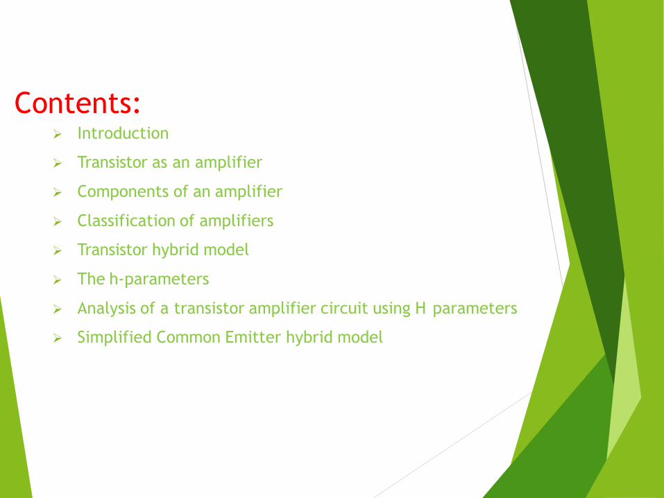
Contents: Introduction
Transistor as an amplifier
Components of an amplifier
Classification of amplifiers
Transistor hybrid model
The h-parameters
Analysis of a transistor amplifier circuit using H parameters
Simplified Common Emitter hybrid model

Introduction
What is Amplifier?
What is the need of an amplifier?
What are the applications of amplifier?

Transistor as an amplifier
To make the transistor work as an amplifier, it is to be biased to
operate in the active region.
When only one transistor with associated circuitry is used for
signal, the circuit is known as “Single Stageamplifying a weak
TransistorAmplifier”.

Components of an amplifier
CEAmplifier

Classification of amplifiers
Based on the active device.
BJTAmplifier
FETAmplifier
Based on the transistor configuration.
Common Emitter amplifier
Common Collectoramplifier
Common Base amplifier
Based on input.
Small signal amplifiers
Large signal amplifiers
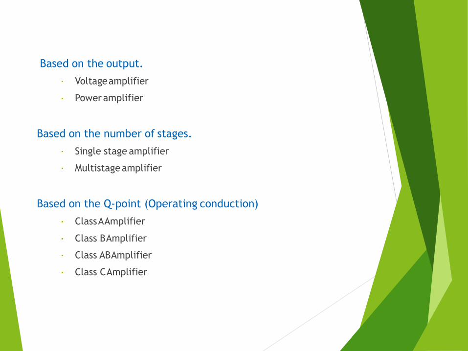
Based on the output.
Voltageamplifier
Poweramplifier
Based on the number of stages.
Single stage amplifier
Multistageamplifier
Based on the Q-point (Operating conduction)
ClassAAmplifier
Class BAmplifier
Class ABAmplifier
Class CAmplifier
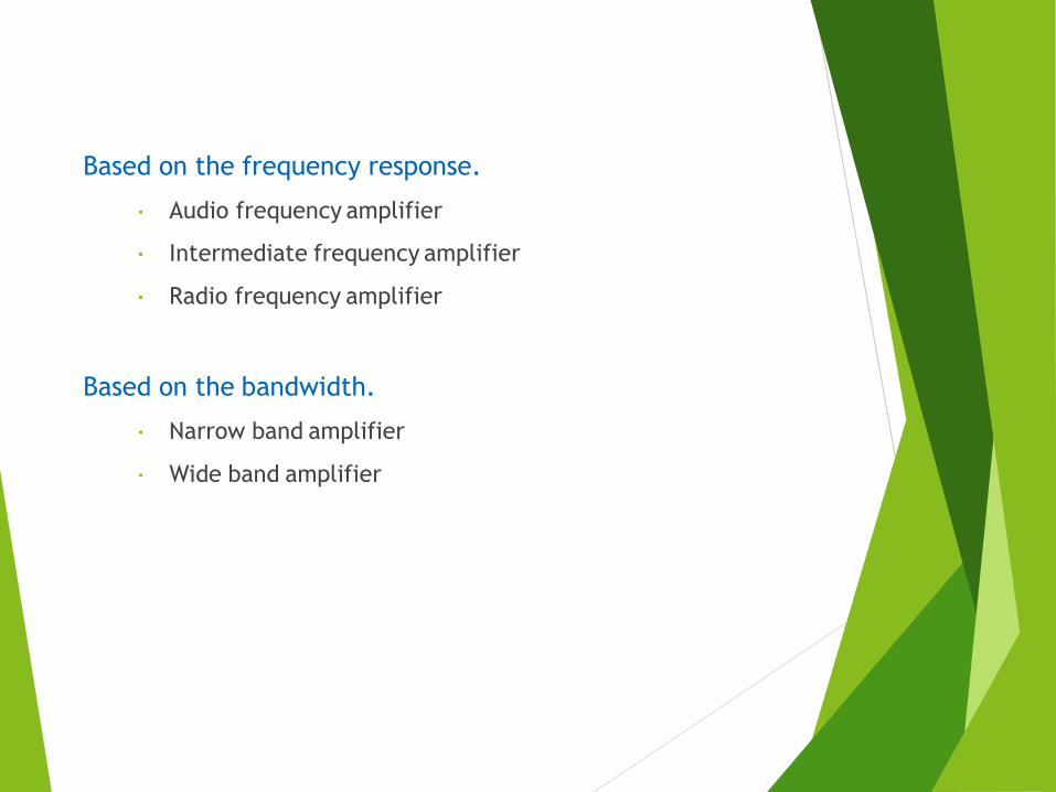
Based on the frequency response.
Audio frequency amplifier
Intermediate frequency amplifier
Radio frequency amplifier
Based on the bandwidth.
Narrow band amplifier
Wide band amplifier

Bipolar junction transistors (BJTs)
NPN BJT shown• 3 terminals: emitter, base, and collector• 2 junctions: emitter-base junction (EBJ) and collector-basejunction (CBJ)
– These junctions have capacitance (high-frequency model)• BJTs are not symmetric devices
–doping and physical dimensions are different for emitter and collector
Construction of Bipolar junction transistors
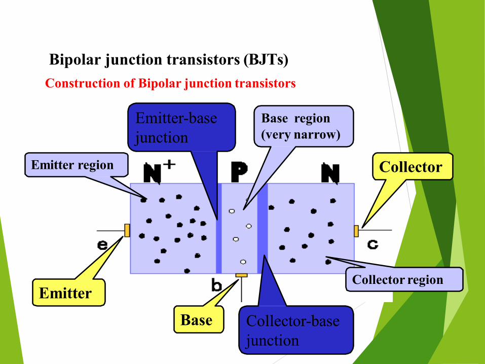
Bipolar junction transistors (BJTs)Construction of Bipolar junction transistors
Base region(very narrow)
Emitter region
Collector region
Collector
Base
Emitter
Emitter-basejunction
Collector-basejunction
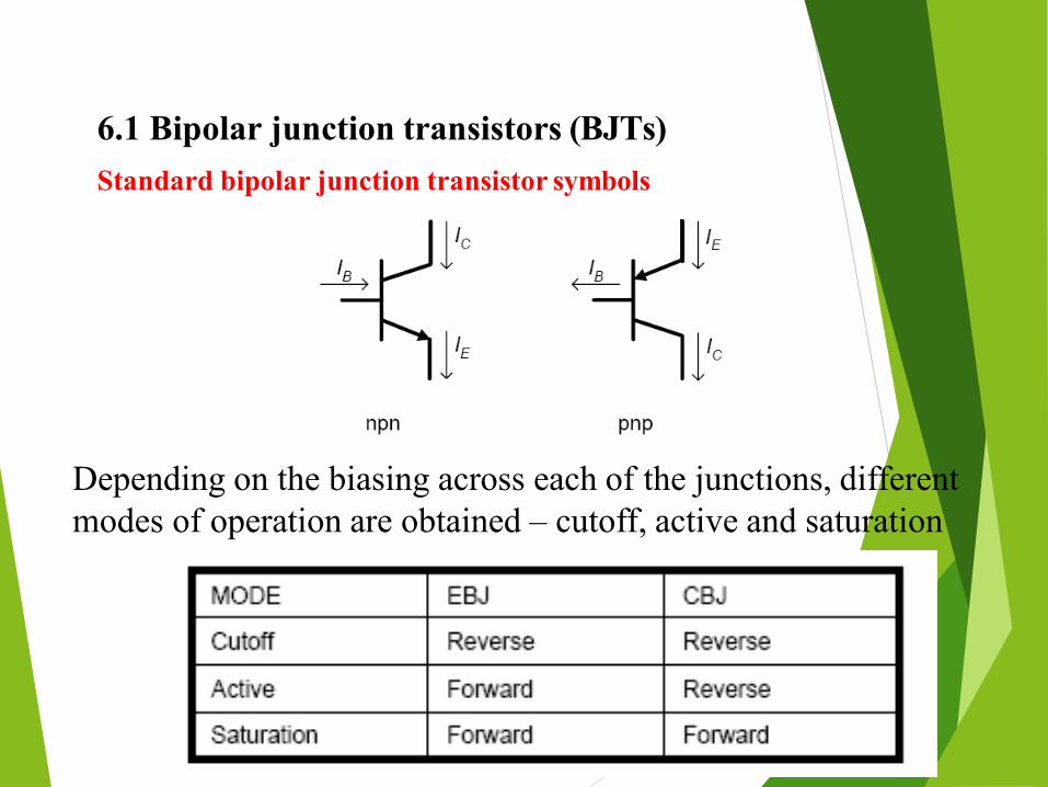
6.1 Bipolar junction transistors (BJTs)Standard bipolar junction transistor symbols
Depending on the biasing across each of the junctions, differentmodes of operation are obtained – cutoff, active and saturation
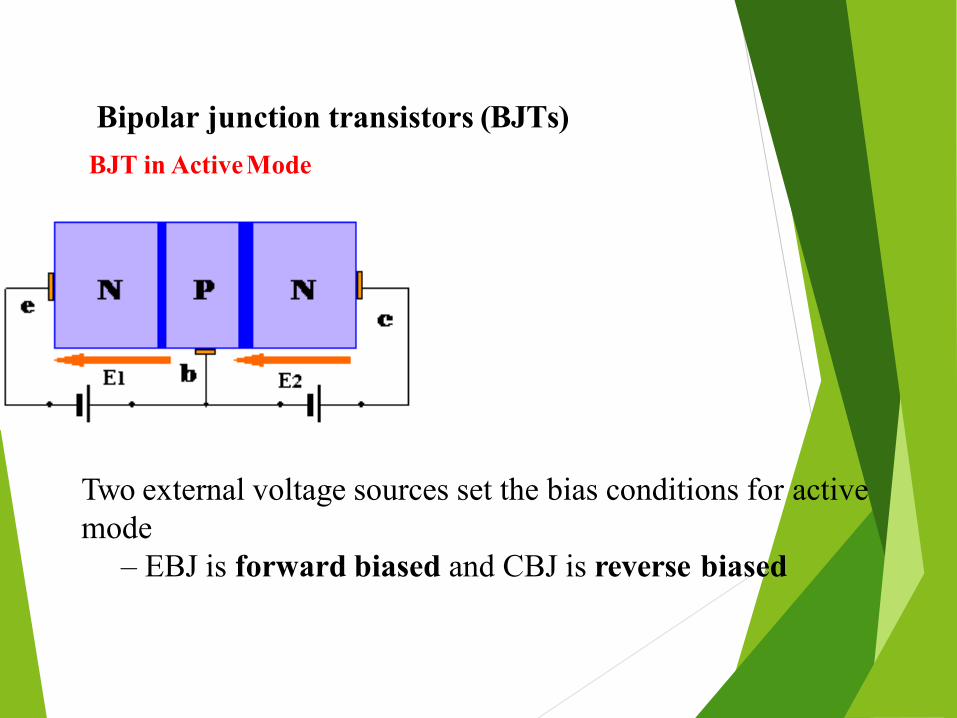
Bipolar junction transistors (BJTs)BJT in ActiveMode
Two external voltage sources set the bias conditions for activemode
– EBJ is forward biased and CBJ is reverse biased
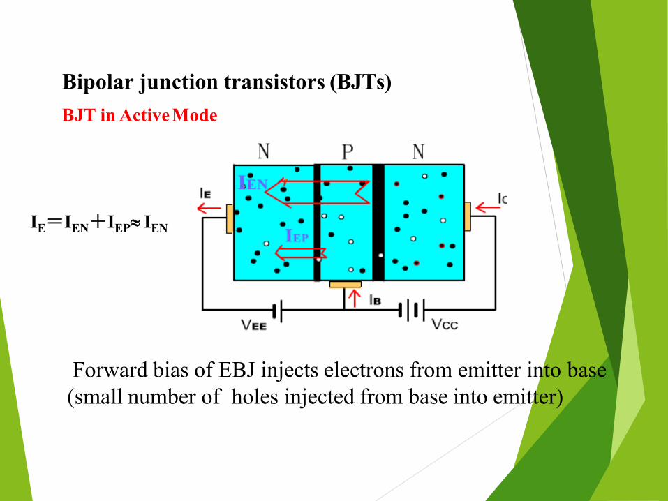
Bipolar junction transistors (BJTs)BJT in ActiveMode
Forward bias of EBJ injects electrons from emitter into base(small number of holes injected from base into emitter)
IE=IEN+IEP IEN

Bipolar junction transistors (BJTs)BJT in ActiveMode
IB =IBN+ IEP
• Most electrons shoot through the base into the collectoracross the reverse bias junction
• Some electrons recombine with majority carrier in (P-type)base region

Bipolar junction transistors (BJTs)BJT in ActiveMode
Electrons that diffuse across the base to the CBJ junction areswept across the CBJ depletion region to the collector.
IC = ICN + ICBO

6.1 Bipolar junction transistors (BJTs)BJT in ActiveMode
IE=IEN+IEP IEN IC = ICN + ICBO
IE = IB + IC
Let ICN=IE
IE
IC---common-base current gain
IC (1-) = IB + ICBO
IB=IBN+IEP
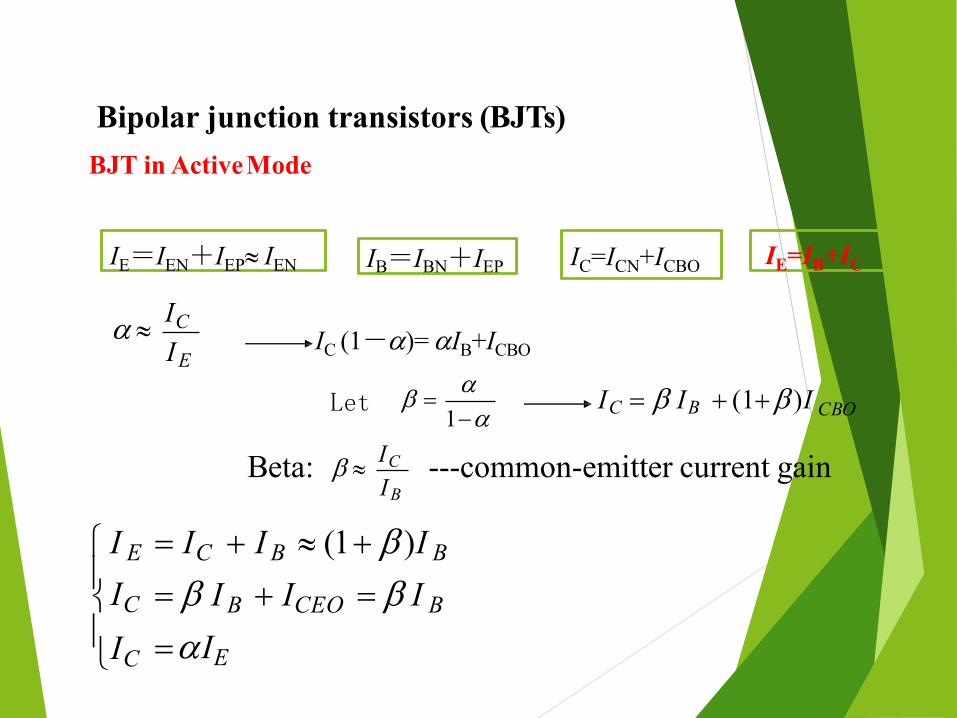
Bipolar junction transistors (BJTs)BJT in ActiveMode
IE=IEN+IEP IEN IC=ICN+ICBO IE=IB+IC
IE
ICIC (1-)=IB+ICBO
IB=IBN+IEP
1Let
I B ICEO I B
IE
I E IC I B (1 )I B
IC
IC
CBO (1)IIC IB
IB
IC ---common-emitter current gainBeta:

Bipolar junction transistors (BJTs)C-E Circuits I-V Characteristics
Base-emitter Characteristic(Input characteristic)
vCECiB f (vBE )

Bipolar junction transistors (BJTs)C-E Circuits I-V Characteristics
Collector characteristic (output characteristic)BCE ) i CiC f(V

Bipolar junction transistors (BJTs)C-E Circuits I-V Characteristics
Collector characteristic
Saturation
Saturation occurs when thesupply voltage, VCC, isacross the total resistance of the collector circuit, RC.
IC(sat) = VCC/RC
Vsat
Once the base current is high enough to produce saturation, further increases inbase current have no effect on the collector current and the relationship IC = IB isno longer valid. When VCE reaches its saturation value, VCE(sat), the base-collectorjunction becomes forward-biased.
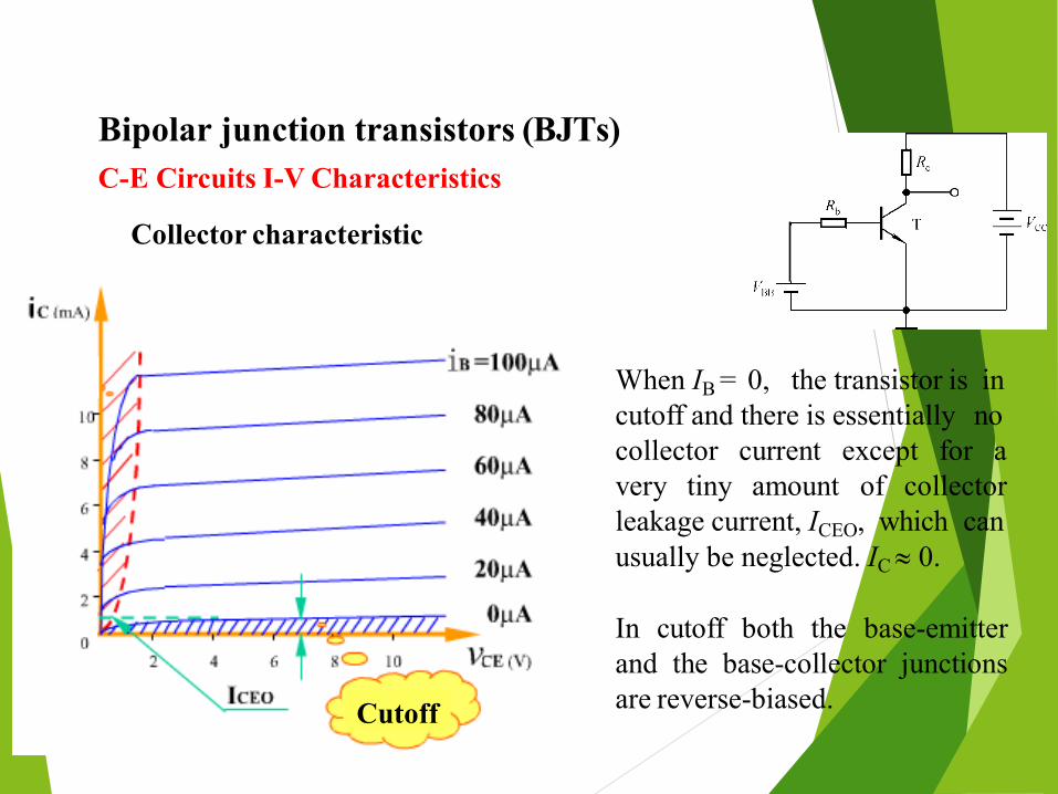
Bipolar junction transistors (BJTs)C-E Circuits I-V Characteristics
Collector characteristic
Cutoff
When IB = 0, the transistor is incutoff and there is essentially nocollectorvery tiny
current except for aamount of collector
leakage current, ICEO, which canusually be neglected. IC 0.
In cutoff both the base-emitterand the base-collector junctionsare reverse-biased.

Bipolar junction transistors (BJTs)DC Load Line and Quiescent Operation Point
DC load line
.QICQ
VCEQ
Q-pointVCC
VCC 40(A)VCC VBE
Rb RbBase-emitter loop: IB
Collector-emitter loop: vCE VCC iCRC 10iC 4k
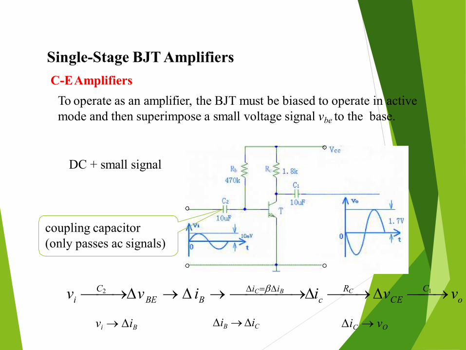
Single-Stage BJT Amplifiers
oCEcBBEiRC vv i iv v C1C2 iCiB
C-EAmplifiersTo operate as an amplifier, the BJT must be biased to operate in activemode and then superimpose a small voltage signal vbe to the base.
DC + small signal
iC vOvi iB iB iC
coupling capacitor(only passes ac signals)
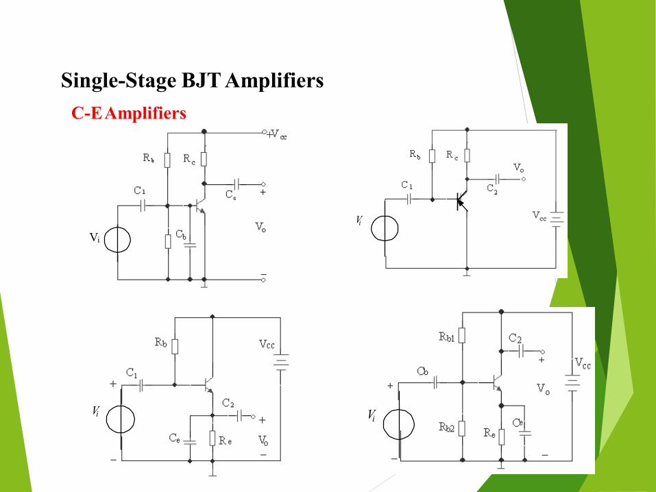
Single-Stage BJT Amplifiers
Vi Vi
C-EAmplifiers+
Vi
Vi
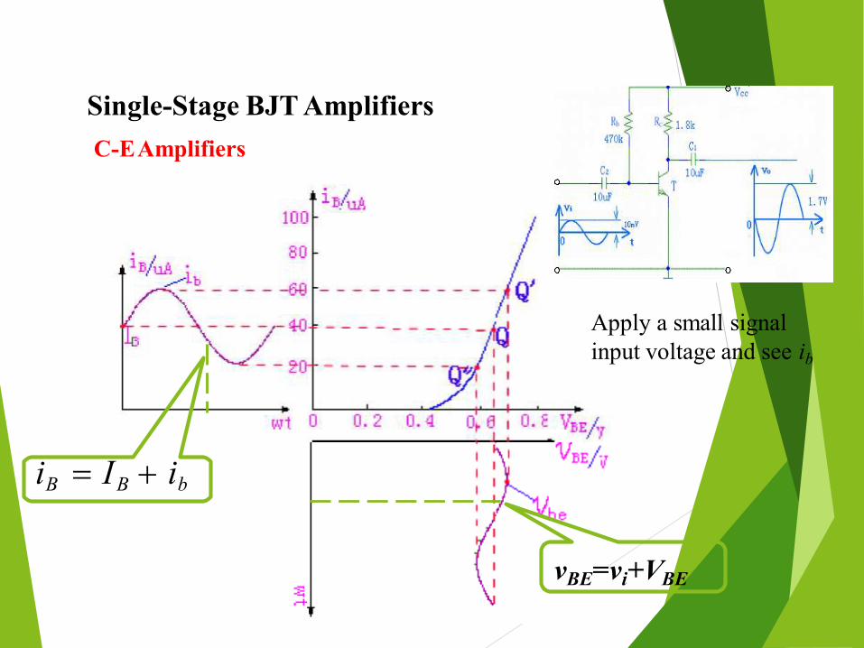
Single-Stage BJT AmplifiersC-EAmplifiers
iB IB ib
vBE=vi+VBE
Apply a small signal input voltage and see ib
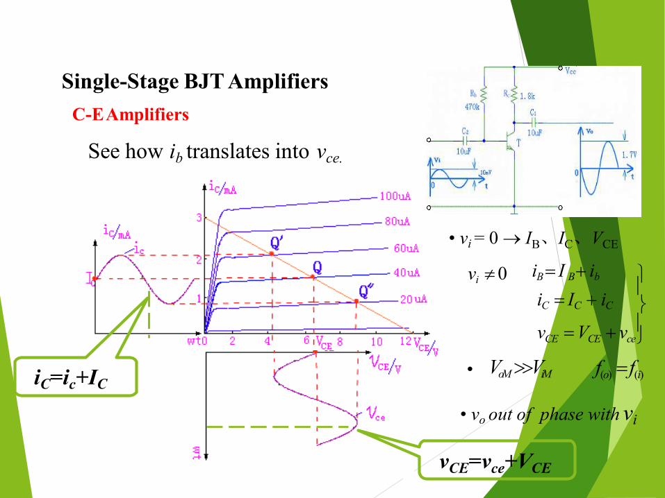
Single-Stage BJT Amplifiers
• vi = 0 IB、IC、VCE
vCE VCE vce
iB I B ib
iC IC iC
vi 0
f(o) f(i)VoM ViM•iC=ic+IC
• vo out of phase with vi
vCE=vce+VCE
C-EAmplifiers
See how ib translates into vce.

Single-Stage BJT AmplifiersC-EAmplifiers (all the capaertors are replaced
by open circuits)CConsidering V
Considering V i (all the capaertors are replaced by short circuits)

Single-Stage BJT AmplifiersC-EAmplifiers
C
by open circuits)Considering V (all the capaertors are replaced
i
by short circuits)Considering V (all the capaertors are replaced
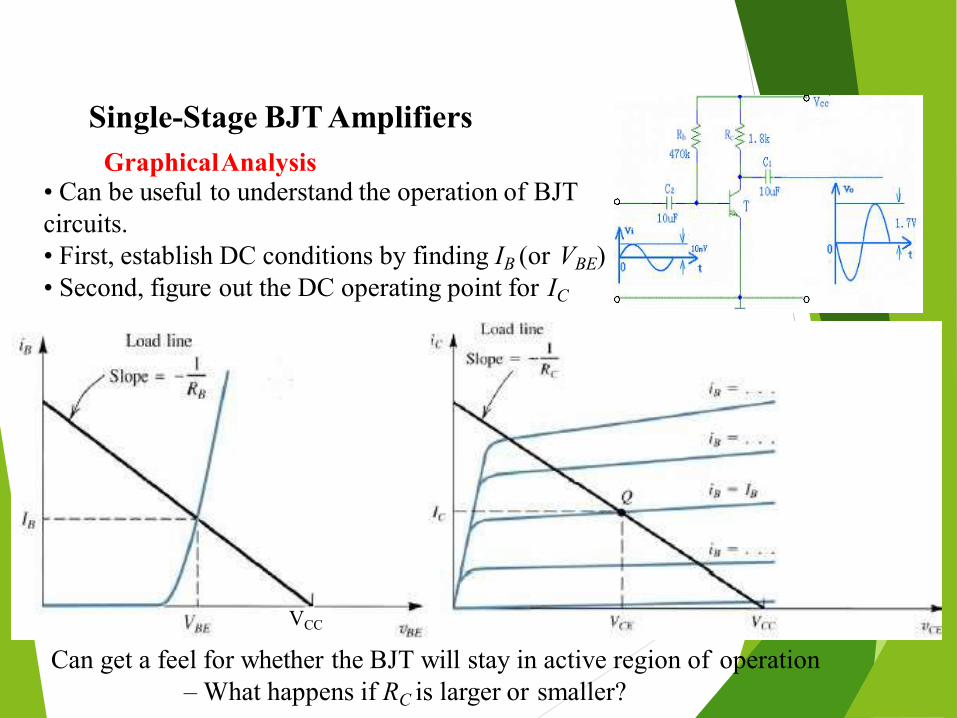
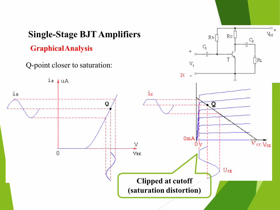
Single-Stage BJT AmplifiersGraphicalAnalysis
• Can be useful to understand the operation of BJTcircuits.• First, establish DC conditions by finding IB (or VBE)• Second, figure out the DC operating point for IC
VCC
Can get a feel for whether the BJT will stay in active region of operation– What happens if RC is larger or smaller?

Single-Stage BJT AmplifiersGraphicalAnalysis
v i (R // R ) i R'ce c C L c L
VCC 'VCEQ ICQRL '
VCC

Single-Stage BJT AmplifiersGraphicalAnalysis
Q-point is centered on the ac load line:
VCC
VCC
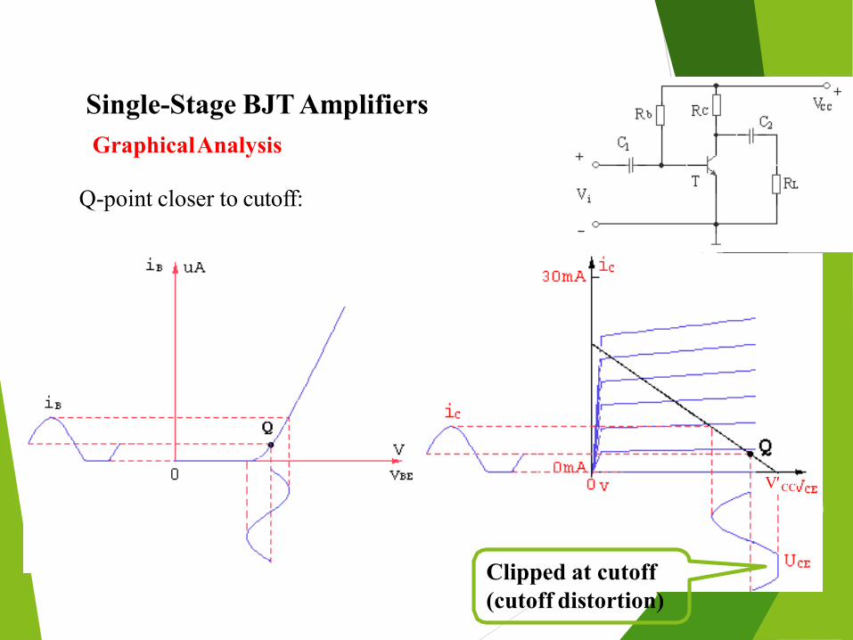
Single-Stage BJT Amplifiers
Clipped at cutoff (cutoff distortion)
GraphicalAnalysis
Q-point closer to cutoff:
VCC
Single-Stage BJT Amplifiers
Clipped at cutoff(saturation distortion)
GraphicalAnalysis
Q-point closer to saturation:

Single-Stage BJT AmplifiersGraphicalAnalysis
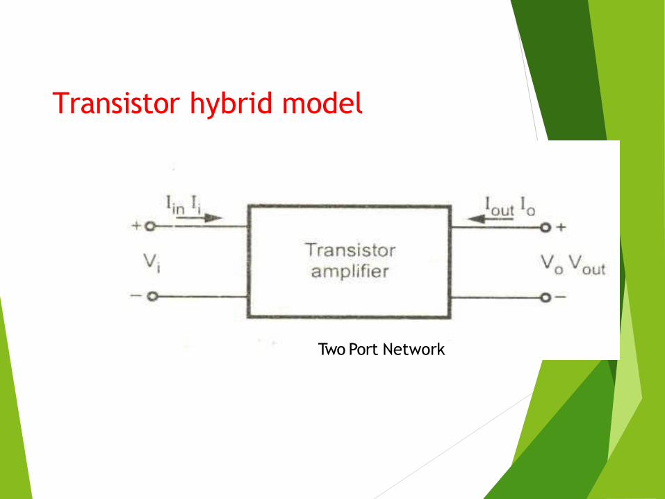
Transistor hybrid model
Two Port Network

Types of Parameters:
i) Z - Parameters (or) Impedance Parameters
ii) Y - Parameters (or) Admittance Parameters
iii) H - Parameters (or) Hybrid Parameters

Z - Parameters (or) Impedance
ParametersHere i1 and i2 are taken as independent variables. The voltages V1 and V2 are given by theequations.
V1 = Z11i1 + Z12i2
V2 = Z21i1 + Z22i2
These four impedance parameters Z11, Z22, Z12 and Z21 are defined as follows.
Z11= V1/i1 with i2=0
Z22= V2/i2 with i1=0
Z12= V1/i2 with i1=0
Z21= V2/i1 withi2=0
= Input impedance with Output port open circuited.
= Output impedance with Input port open circuited.
= Reverse Transfer impedance with port1 open circuited.
= Forward Transfer impedance with port2 open circuited.
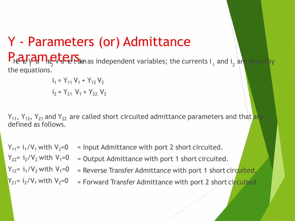
Y - Parameters (or) Admittance
1 2 1 2PHearerVaamndeVtaerertsaken as independent variables; the currents i and i are given by
the equations.
i1 = Y11 V1 + Y12 V2
i2 = Y21 V1 + Y22 V2
Y11, Y12, Y21 and Y22 are called short circuited admittance parameters and that aredefined as follows.
Y11= i1/V1 with V2=0
Y22= i2/V2 with V1=0
Y12= i1/V2 with V1=0
Y21= i2/V1 with V2=0
= Input Admittance with port 2 short circuited.
= Output Admittance with port 1 short circuited.
= Reverse Transfer Admittance with port 1 short circuited.
= Forward Transfer Admittance with port 2 short circuited.

H - Parameters (or) Hybrid ParametersIf the input current i1 and the output voltage V2 are taken as independent variables,
the input voltage V1 and output current i2 can be written as
V1 = h11 i1 + h12 V2
i2 = h21 i1 + h22 V2
The four hybrid parameters h11, h12, h21 and h22 are defined asfollows.
= Input impedance with output port short circuited.
= Output Admittance with input port open circuited.
= Reverse Voltage Transfer ratio with input port open
h11= V1/i1 with V2=0
h22= i2/V2 with i1=0
h12= V1/V2 with i1=0
circuited.
h21= i2/i1 with V2=0 = Forward current gain with output port short circuited.
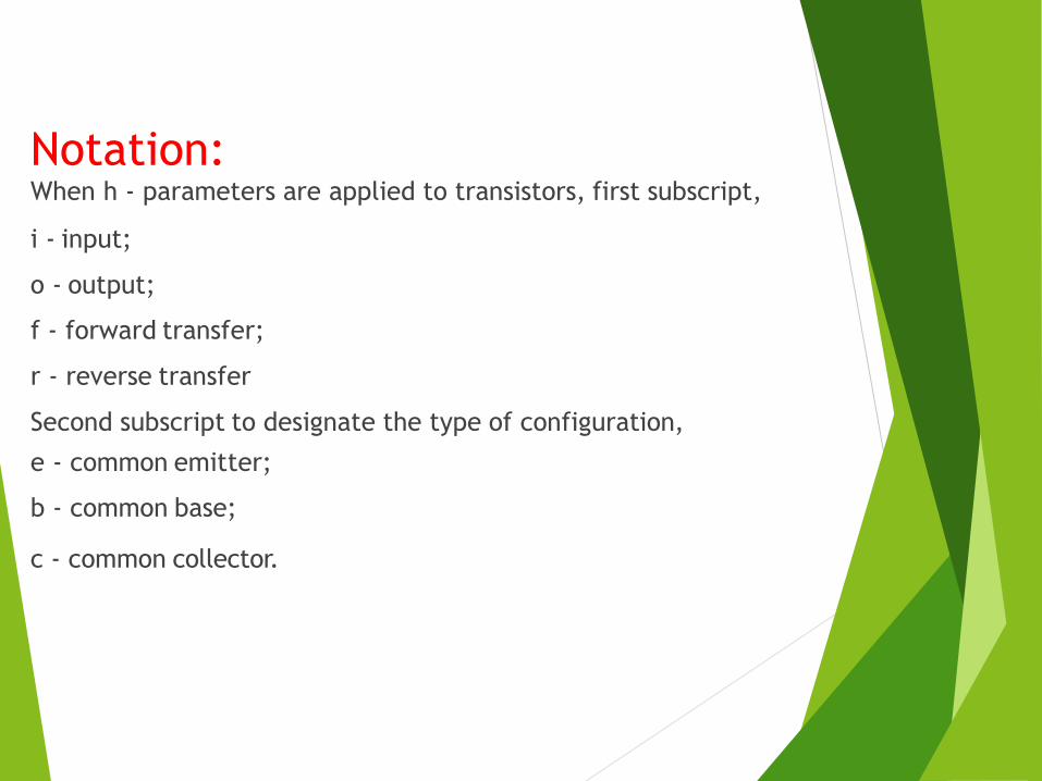
Notation:When h - parameters are applied to transistors, first subscript,
i - input;
o - output;
f - forward transfer;
r - reverse transfer
Second subscript to designate the type of configuration,
e - common emitter;
b - common base;
c - common collector.

The Hybrid model for two - port
network V1 = hi i1 + hr V2
i = h i + h V2 f 1 0 2
Hybrid model for two-port network

Hybrid models for the transistor in three different
configurations

Typical Values
Parameters CE CC CB
hi 1,100 Ω 1,100 Ω 21.6 Ω
hr 2.5x10⁻⁴ 1 2.9x10⁻⁴
hf 50 -51 -0.98
ho 25 μA/v 25 μA/v 0.49 μA/v
1/h0 40K 40K 2.04MΩ
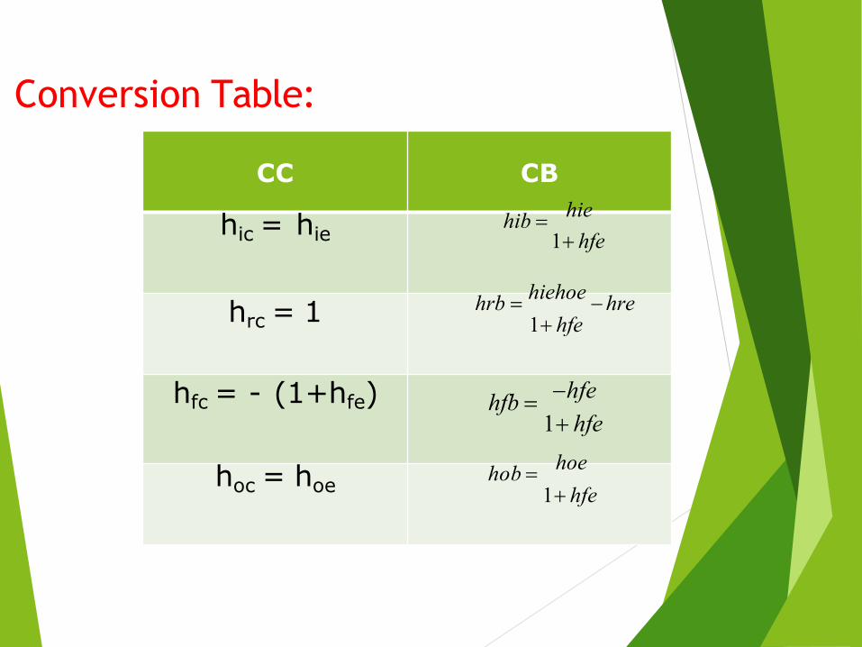
Conversion Table:
CC CB
hic = hiehib hie
1 hfe
hrc = 1 hrb hiehoe hre
1 hfe
hfc = - (1+hfe) hfb hfe1 hfe
hoc = hoehob hoe
1 hfe

Analysis of a Transistor Amplifier Circuit
Using h– Parameters
Basic Amplifier circuit
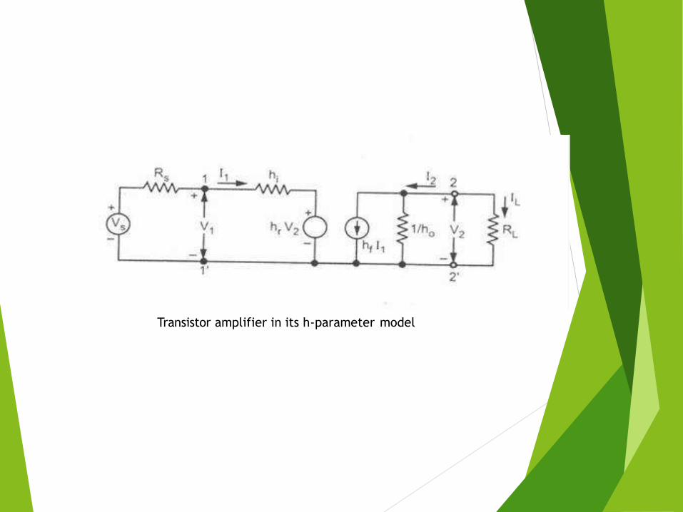
Transistor amplifier in its h-parameter model

Current Gain:
Voltage Gain:
Input Impedance:
OutputAdmittance:
PowerGain:
IL
h fA 1 hoZ
ViZ
A AI ZL
0 0ih
h hY h f r
2 LP I
R A A
Ri

Current Gain With Source Resistance:
Voltage Gain With Source Resistance:
Input Impedance With Source Resistance: Zis = Rs+Zi
Output Admittance With Source Resistance:
V Si S
AIZLA Z R
hf hrY0 h0 RS hi
R. S
ZL
AIS AVS
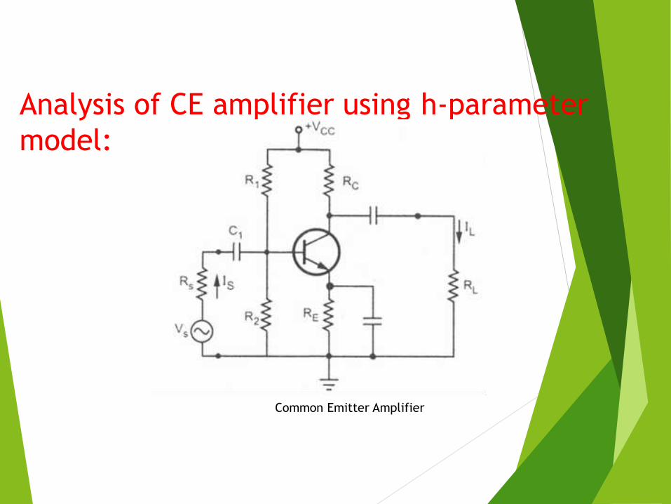
Analysis of CE amplifier using h-parameter
model:
Common Emitter Amplifier
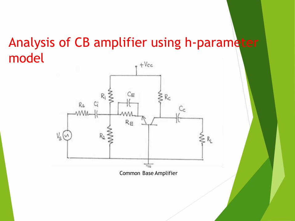
Analysis of CB amplifier using h-parameter
model
Common Base Amplifier
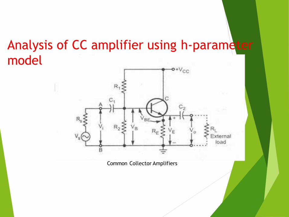
Analysis of CC amplifier using h-parameter
model
Common Collector Amplifiers
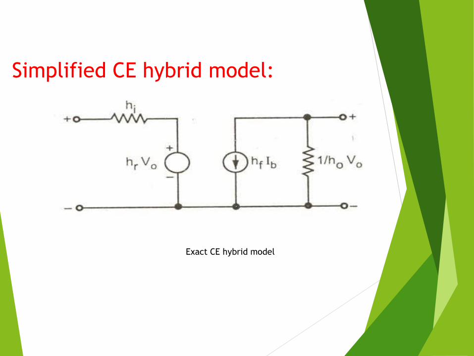
Simplified CE hybrid model:
Exact CE hybrid model

Approximate CE hybrid model
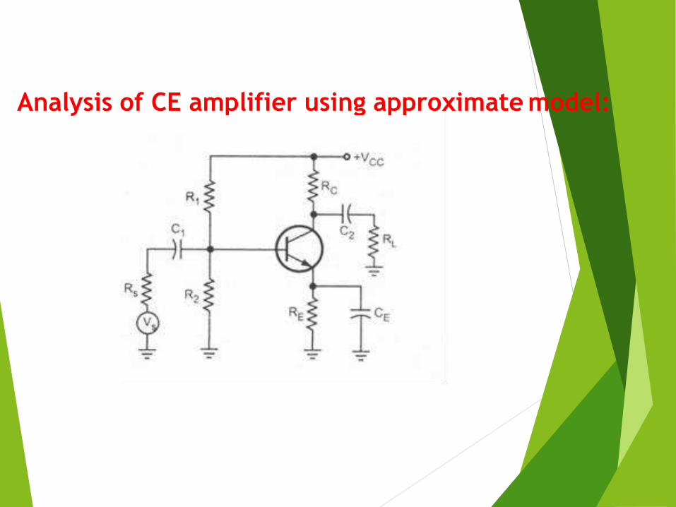
Analysis of CE amplifier using approximate model:
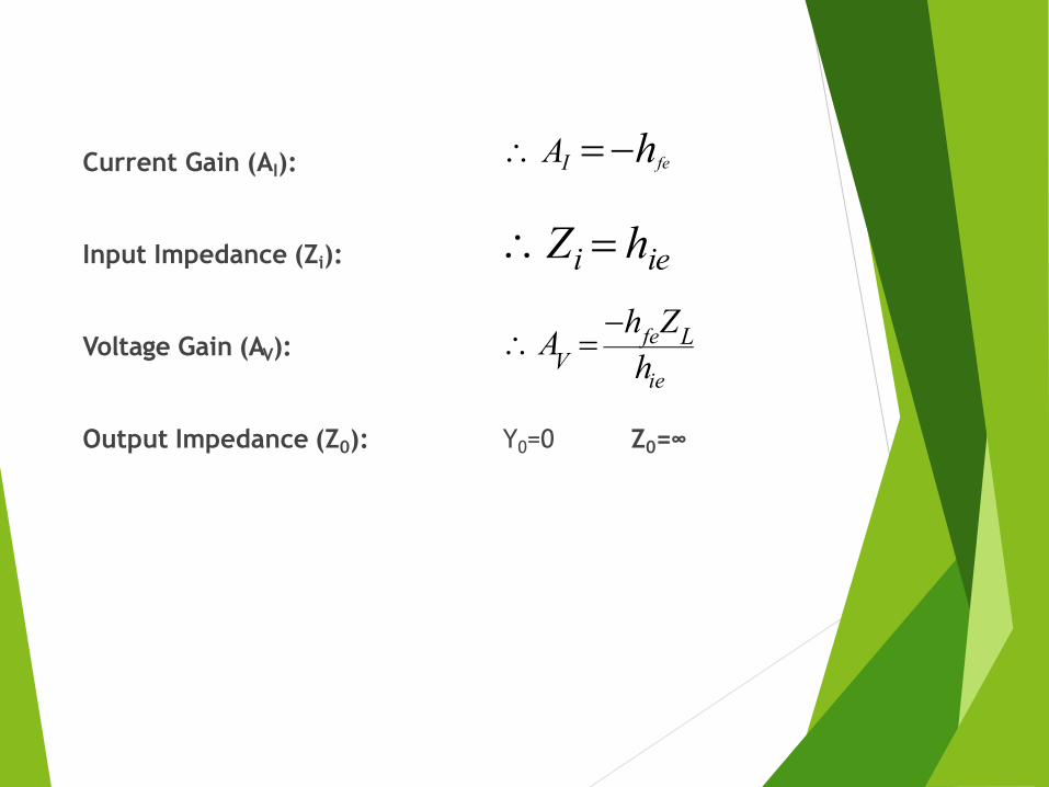
Current Gain (AI):
Input Impedance (Zi):
Voltage Gain (AV):
Output Impedance (Z0): Y0=0 Z0=∞
AI hfe
ieV h
Zi hie
h ZA fe L

Characteristics of CBAmplifier:
i) Current gain of less than unity.
ii) High voltage gain.
iii) Power gain approximately equal to voltage gain.
iv) No phase shift for current (or) voltage.
v) Small input impedance.
iv) Large output impedance.
Applications:
1) Matching a very low impedance source.
2) As a non-inverting amplifier with voltage gain exceedingunity.
3) For driving a high impedance load.
4) As a constant current source.
Characteristics of CC Amplifier:
1) High current gain.
2) Voltage gain of approximately unity.
3) Power gain approximately equal to current gain.
4) No current (or) voltage phase shift.
5) Large input impedance.
6) Small output impedance.
Applications:
The CC amplifier is widely used as a buffer stage between a high impedance
source and a low impedance load. The CC amplifier is called the emitter follower
Characteristics of CE amplifier:
1. Large current gain.
2. Large voltage gain.
3. Large power gain.
4. Voltage phase shift of 1800.
5. Moderate input impedance.
6. Moderate output impedance.
Applications:
Of the three configurations CE amplifier alone is capable of providing both voltage gain and current gain. The input resistance Ri and the output resistance Ro are moderately high.
Hence the CE amplifier is widely used for amplification purpose.

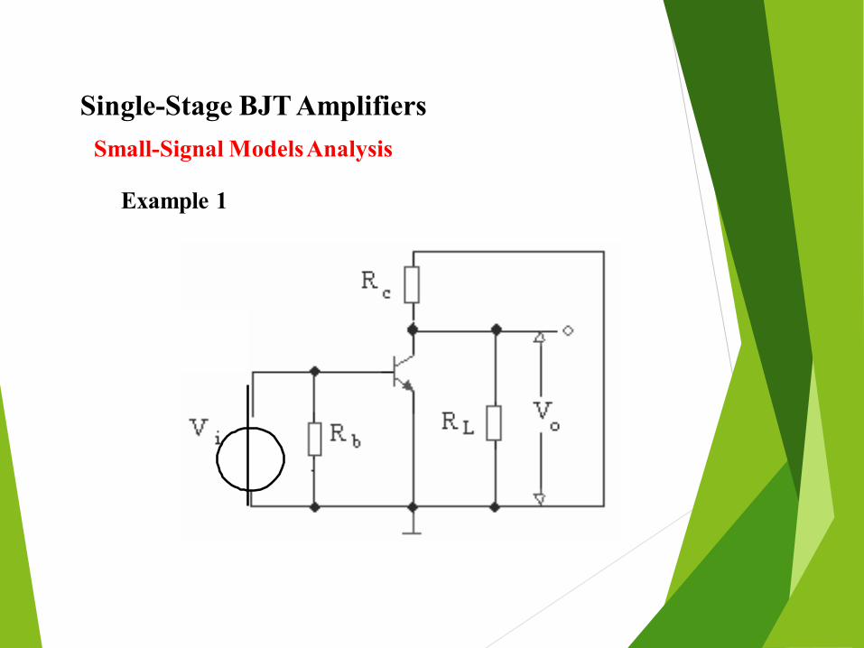
Single-Stage BJT AmplifiersSmall-Signal ModelsAnalysis
Steps for using small-signal models1. Determine the DC operating point of the BJT
- in particular, the collector current2. Calculate small-signal model parameters: rbe3. Eliminate DC sources
– replace voltage sources with shorts and currentsources with open circuits
4. Replace BJT with equivalent small-signal models5. Analysis

Single-Stage BJT AmplifiersSmall-Signal ModelsAnalysis
IC ≈ βIB,IE = IC + IB = (1+β)IB
VC (IB IC )R IBRb VBE IERe
BVC VBE
I Rb (1 )(R Re )
VCE VC IC RC IE (R Re )
Single-Stage BJT AmplifiersSmall-Signal ModelsAnalysis
Example 1

Single-Stage BJT AmplifiersSmall-Signal ModelsAnalysis
Example 2
vs
B VCCb1 b2
Rb2
R RV
Be
EC RV / Re
VB VBEI I
ICIB
VCE VCC IC (RC Re )

Single-Stage BJT AmplifiersSmall-Signal ModelsAnalysis
There are three basic configurations for single-stageBJT amplifiers:
– Common-Emitter– Common-Base– Common-Collector
VBB VCC
RC
N P N ce
bVBB VCC
RcN
NP
c
e
bVBB
VCC
Re
NP
e
b N
c
(c)(a)
VE VB VC
(b)
VE VB VCVE VB VC

Single-Stage BJT AmplifiersCommon-CollectorAmplifier
VCC IBRb VBE IE Re IB Rb VBE (1)IB Re
e b eB
VCC VBE VCCI R (1 )R R 1 Rb
IC IB
VCC VCE IE Re VCE IC Re
VCE VCC IC Re
Note : Vo is slightly less thanVi due to the voltage drop introduced by VBE
AV 1

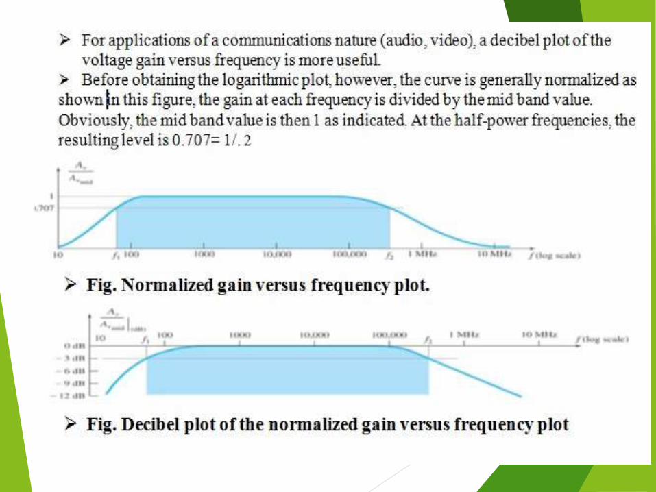
Frequency ResponseBasic Concepts
Av ( f )( f) or A Av ()()Av
Lower cut off frequency Upper cut off frequency
The drops of voltage gain (output/input) is mainly due to:1、Increasing reactance of (at low f)2、Porasitic capacetine elemCesn,tCs ocf,Cthee net work (at high f)3、Dissappearance of changing current(for trasformer coupled amp)

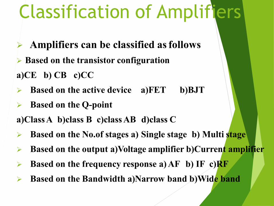
Classification of Amplifiers
Amplifiers can be classified as follows Based on the transistor configurationa)CE b) CB c)CC Based on the active device a)FET b)BJT Based on the Q-pointa)Class A b)class B c)class AB d)class C Based on the No.of stages a) Single stage b) Multi stage Based on the output a)Voltage amplifier b)Current amplifier Based on the frequency response a) AF b) IF c)RF Based on the Bandwidth a)Narrow band b)Wide band
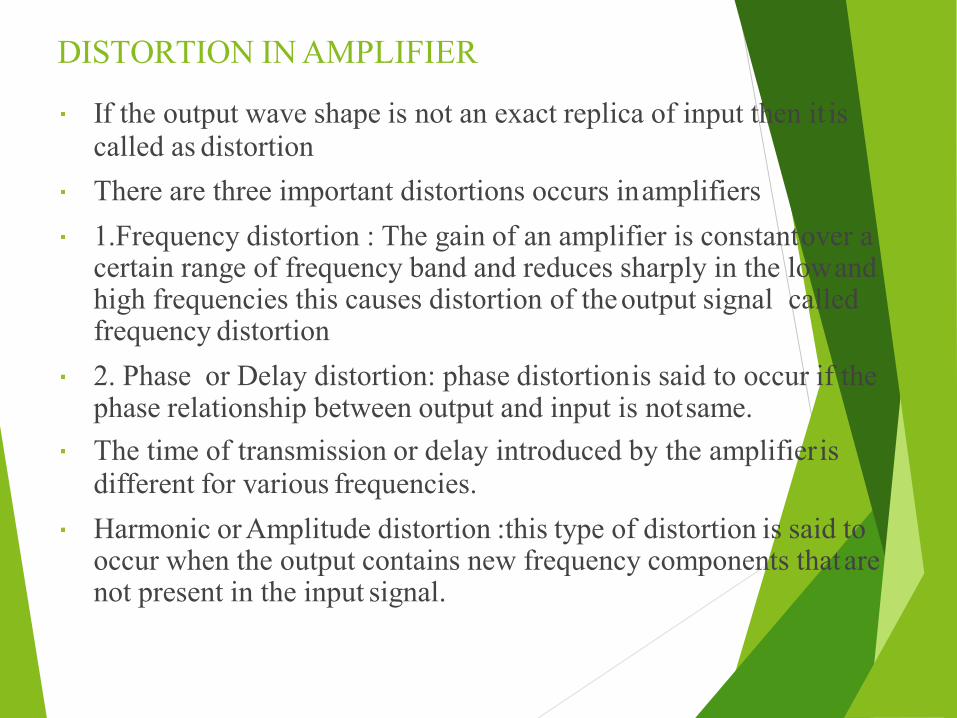
DISTORTION IN AMPLIFIER
If the output wave shape is not an exact replica of input then it iscalled as distortionThere are three important distortions occurs inamplifiers1.Frequency distortion : The gain of an amplifier is constantover a certain range of frequency band and reduces sharply in the lowand high frequencies this causes distortion of theoutput signal called frequency distortion2. Phase or Delay distortion: phase distortionis said to occur if the phase relationship between output and input is notsame.The time of transmission or delay introduced by the amplifierisdifferent for various frequencies.Harmonic or Amplitude distortion :this type of distortion is said to occur when the output contains new frequency components thatare not present in the input signal.

CE,CB,CC Amplifiers comparison
Property CB CE CCRi Low(about 100Ω) Moderate(about 750Ω) High(about750kΩ)
Ro High (about 450kΩ) Moderate(about 45kΩ) Low(about 25Ω)
AiAv
1about 150
High Highabout 500 Less than 1
Phase shift b/w i/p & o/p (Degrees) 0 or 360 180 0 or 360
Applications:for high frequency circuits, for AF circuits ,for impedance matching

Unit-1(b)
FEEDBACK AMPLIFIERS
70

Agenda
Introduction
Need of Feedback
Types of Feedback
Classification of Feedback
Working and Analysis
Results
Applications
71
72
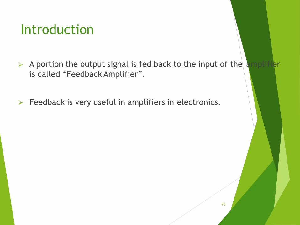
Introduction
A portion the output signal is fed back to the input of the amplifier
is called “Feedback Amplifier”.
Feedback is very useful in amplifiers in electronics.
73

Need of Feedback
of precision VLSI circuits is Practical realization
complicated
Why---
1. physical circuit components deviate from nominal
values due to temperature, process variation
2. circuit performance changes with frequency, load
variations
74

There are two types of feedbacks.
1. Positive feedback
Source signal +feedback Signal → circuit
2. Negative feedback
Source signal - feedback Signal input → circuit
75

Positive Feedback
If the feedback signal Xf is in phase with input signal
Xs, then the type of feedback is said to be positive
(or) regenerative feedback.
For positive feedback, Xi=Xs+Xf
Xs=Xi-Xf
Gain of the amplifier with feedback,
76
A f A
1 A

The product of the open loop gain and the feedback
factor is called the Loop gain = Aβ.
Gain is Infinity.
Positive feedback increases the instability of an
amplifier, reduces the bandwidth and increases the
distortion and noise.
77
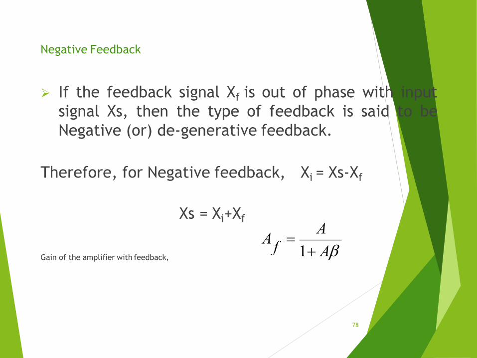
Negative Feedback
If the feedback signal Xf is out of phase with input
signal Xs, then the type of feedback is said to be
Negative (or) de-generative feedback.
Therefore, for Negative feedback, Xi = Xs-Xf
Xs = Xi+Xf
Gain of the amplifier with feedback,
78
AfA
1 A

If where β is a feedback
ratio. The gain may be made to depend entirely in
the feedback network.
If the feedback network contains only stable passive
elements, the gain of the amplifier using Negative
feedback is also stable.
79
A 1 thenAf 1
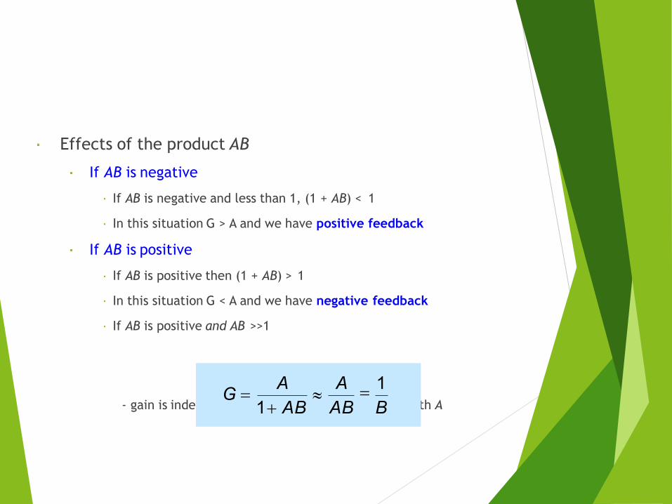
Effects of the product AB
If AB is negative
If AB is negative and less than 1, (1 + AB) < 1
In this situation G > A and we have positive feedback
If AB is positive
If AB is positive then (1 + AB) > 1
In this situation G < A and we have negative feedback
If AB is positive and AB >>1
- gain is independent of the gain of the forward path A
A A
1
1 AB AB BG

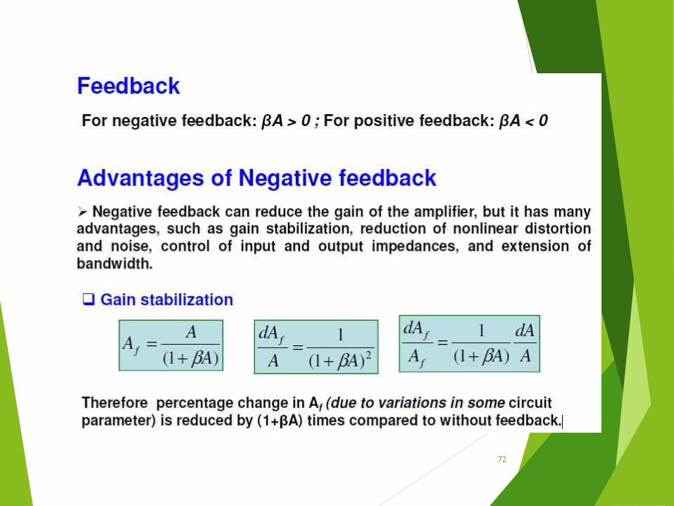
Negative Feedback Properties
Negative feedback takes a sample of the output signal andapplies it to the input to get several desirable properties. Inamplifiers, negative feedback can be applied to get thefollowing properties
Desensitized gain : gain less sensitive to circuitcomponent variations
Gain of the amplifier with feedback,
Differentiate on both sides then, we get
Sensitivity81
AfA
1 A
dA 1dAf
A 1 AAf
dAf
Af
dA A
1
1 A

82

83

84

Effects on input and output resistance
Negative feedback can either increase or decrease the input or output resistance depending on how it is used.
if the output voltage is fed back this tends to make the output voltage more stable by decreasing the output resistance
if the output current is fed back this tends to make the output current more stable by increasing theoutput resistance
if a voltage related to the output is subtracted from the input voltage this increases the input resistance
if a current related to the output is subtracted from the input current this decreases the inputresistance
the factor by which the resistance changes is (1 + AB)
86

Contd…
Extend bandwidth of amplifier1. The product o voltage gain and bandwidth of an amplifier without feedback and with
feedback remains the same.i.e., Af. (B.Wf) = A. (B.W)
87
Contd…
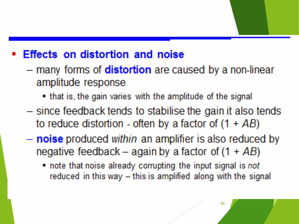
Reduce nonlinear distortion : output proportional to input(constant gain independent of signal level)
Reduce effect of noise
Control input and output impedances by applyingappropriate feedback topologies
88
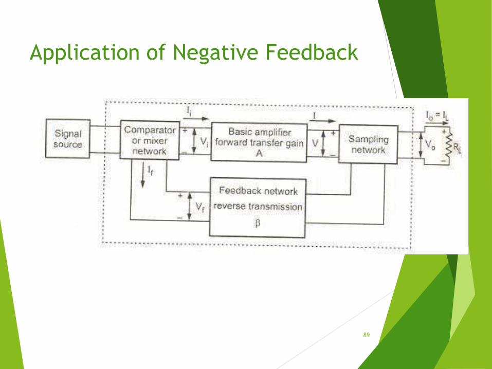
Application of Negative Feedback
89
Current sampling
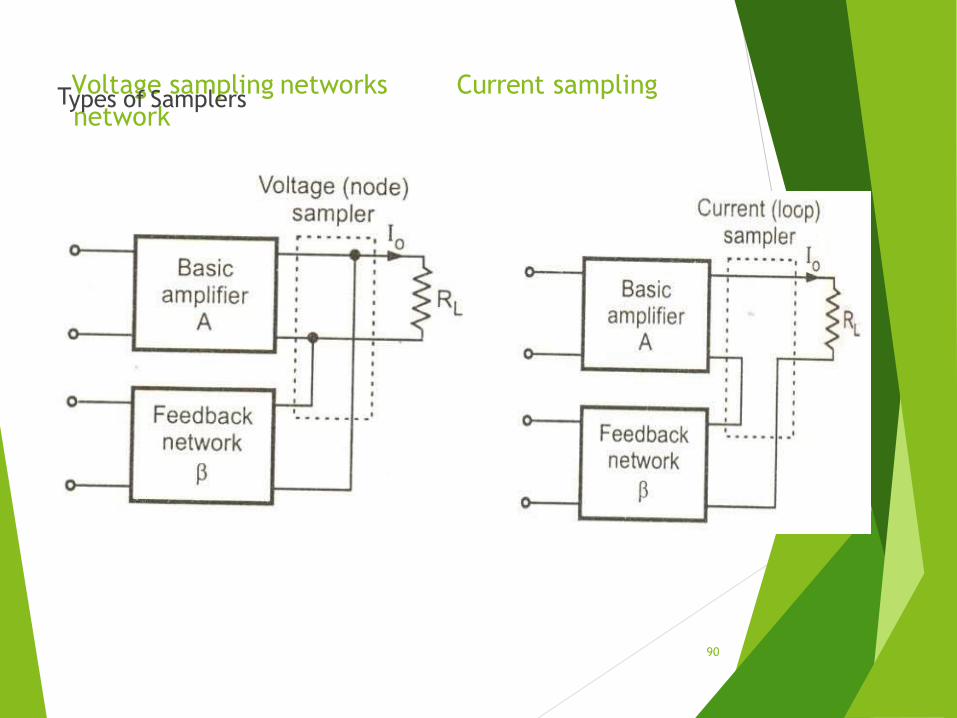
networkTVoltage sampling networksypes of Samplers
90

Types of Mixers
91
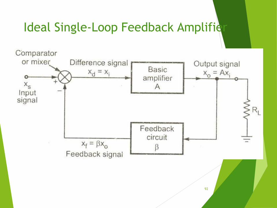
Ideal Single-Loop Feedback Amplifier
92
Classification of Amplifiers
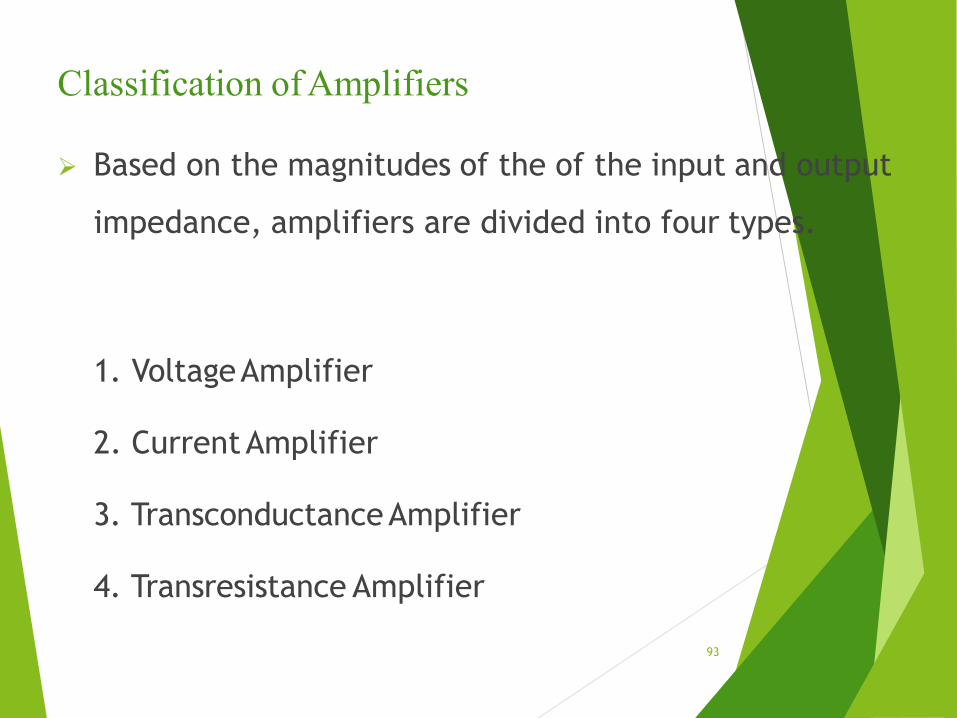
Based on the magnitudes of the of the input and output
impedance, amplifiers are divided into four types.
1. VoltageAmplifier
2. CurrentAmplifier
3. TransconductanceAmplifier
4. Transresistance Amplifier
93
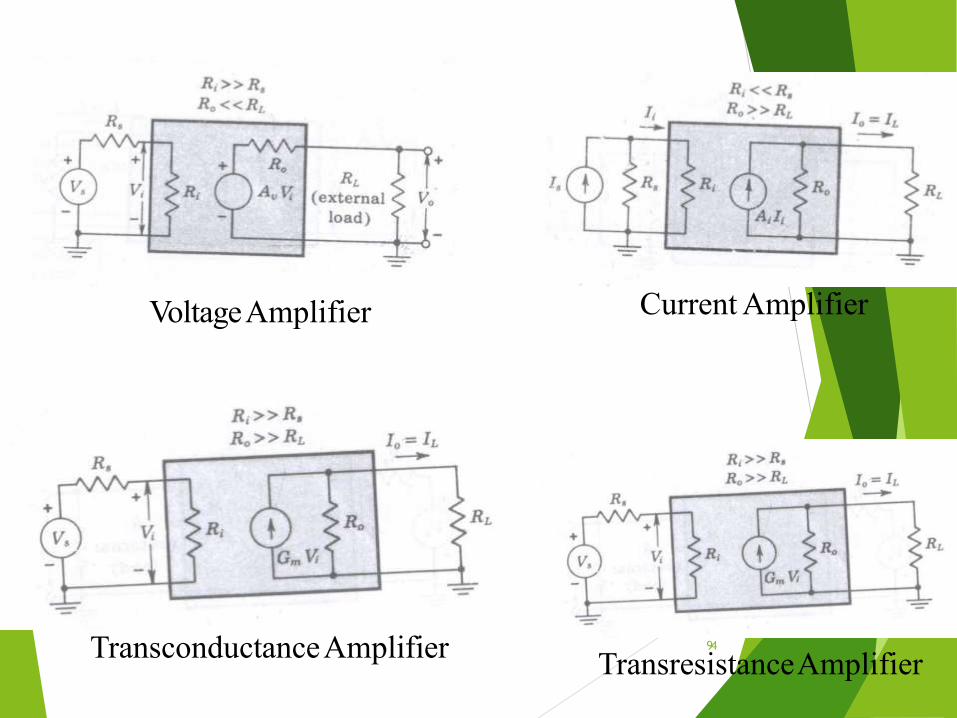
VoltageAmplifier Current Amplifier
TransconductanceAmplifier 94
TransresistanceAmplifier

Basic Feedback Topologies
Depending on the input signal (voltage or current) to be amplified andform of the output (voltage or current), amplifiers can be classified intofour categories. Depending on the amplifier category, one of four typesof feedback structures should beused.
(Type of Feedback)
(1) Series (Voltage)
(2) Series (Voltage)
(3) Shunt (Current)
(4) Shunt (Current)
(Type of Sensing)
Shunt (Voltage) (VoltageAmplifier)Series (Current) (TransconductanceAmplifier)
Shunt (Voltage) (Transresistance Amplifier)
Series (Current) (CurrentAmplifier)95

The four basic feedback topologies: (a) voltage-sampling series mixing (series-shunt) topology; (b) current-sampling shunt mixing (shunt-series) topology; (c) current-sampling seri9e6s-mixing (series-series)
topology; (d) voltage-sampling shunt-mixing (shunt-shunt) topology.
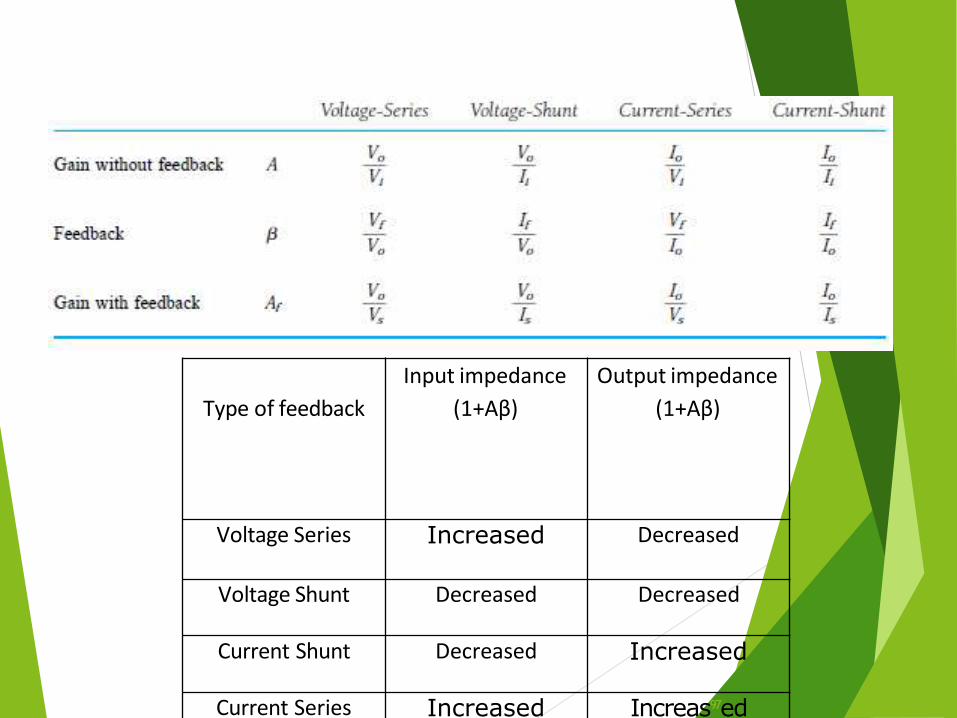
Type of feedback
Input impedance
(1+Aβ)
Output impedance
(1+Aβ)
Voltage Series Increased Decreased
Voltage Shunt Decreased Decreased
Current Shunt Decreased Increased
Current Series Increased Increas97ed
Feedback Amplifier
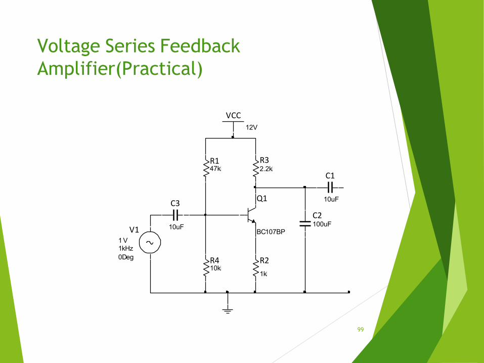
Voltage Series Feedback
Amplifier(Practical)
99
Q1
BC107BPV11 V1kHz 0Deg
VCC
12V
C1
10uF
C2100uF
R147k
R2
1k
R32.2k
R410k
C3
10uF

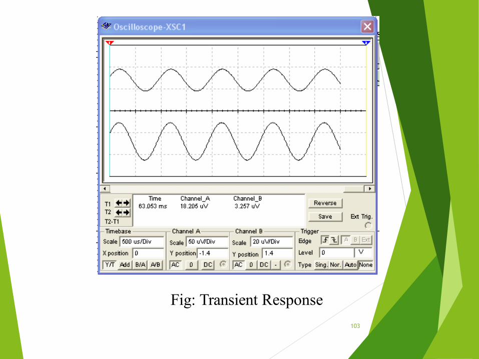
100
Fig: Transient response
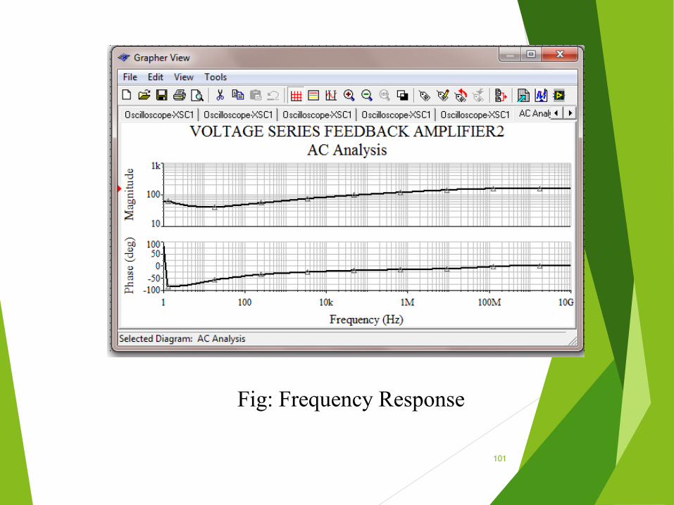
101
Fig: Frequency Response

Current Shunt Feedback Amplifier(Practical)
102
Q1
2N2222A
Q2
2N2222A
RS
500
Rc110k
Re12k
R147k
R25k
5kR4 Re2
2k
Rc210kR3
47k
RL10k
Vs
0.01mV1kHz0Deg
C1
1.0uF
C3
1.0uF
C2
1.0uF
C4
1.0uF
R5
4.7k
VDD
12V
10
2
103
Fig: Transient Response
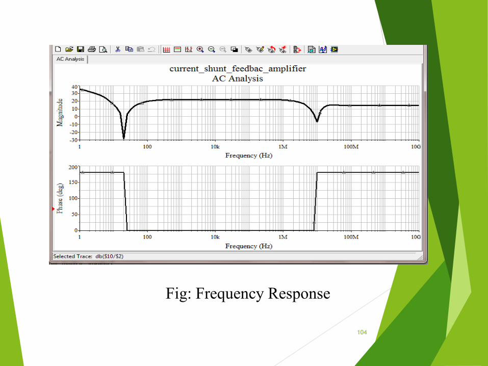
104
Fig: Frequency Response

MethodologyStep 1: Identify topology. (Type offeedback).
To find the type of samplingnetwork
By shorting the output i.e., Vo=0, if feedback signal (Xf) becomes zero then we can say that it is “VoltageSampling”.
By opening the output loop i.e., Io=0,if feedback signal (Xf) becomes zero then we can say that it is “Current Sampling”.
To find the type of mixingnetwork.
If the feedback signal is subtracted from the input voltage source, then wecan say that it is “Series Mixing”.
If the feedback signal is subtracted from the input current source, then we can say that it is “Shunt Mixing”.
105

Step 2: To find the input circuit.
For voltage sampling Vo=0
For current sampling Io=0
Step 3: To find the output circuit.
For series mixing Ii=0
For shunt mixing Vi=0
Step 4: Replace the active device by its h-parameter model at low frequency.
Find the open loop gain (without feedback), ‘A’ of the amplifier.
Indicate Xf and Xo on the circuit and evaluate.
Step 5:
Step 6:
Step 7: From ‘A’ and ‘β’ find Af, Rif, Rof. 106

107

UNIT-II:
BJT & FET Frequency Response
108


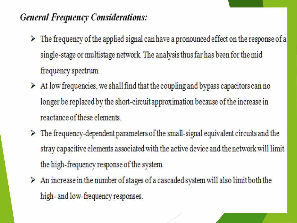
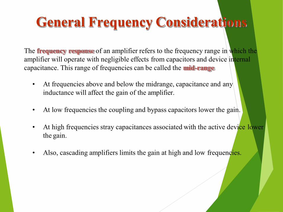
General Frequency Considerations
The frequency response of an amplifier refers to the frequency range in which the amplifier will operate with negligible effects from capacitors and device internal capacitance. This range of frequencies can be called the mid-range.
• At frequencies above and below the midrange, capacitance and anyinductance will affect the gain of the amplifier.
• At low frequencies the coupling and bypass capacitors lower the gain.
• At high frequencies stray capacitances associated with the active device lowerthe gain.
• Also, cascading amplifiers limits the gain at high and low frequencies.

Bode Plot
A Bode plot indicates thefrequency response of anamplifier.
The horizontal scale indicates the frequency (in Hz) and the vertical scale indicates the gain (in dB).
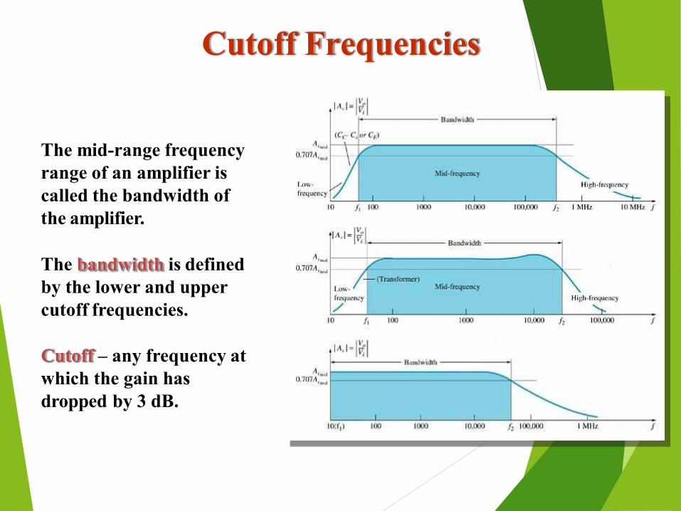
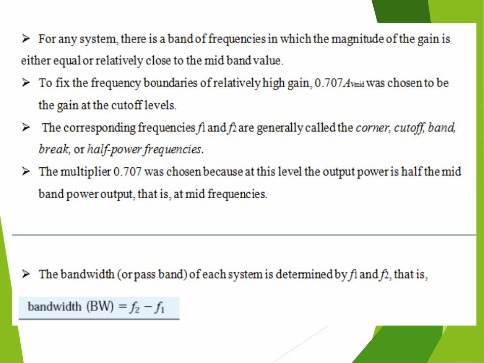
Cutoff Frequencies
The mid-range frequency range of an amplifier is called the bandwidth of the amplifier.
The bandwidth is defined by the lower and upper cutoff frequencies.
Cutoff – any frequency at which the gain has dropped by 3 dB.
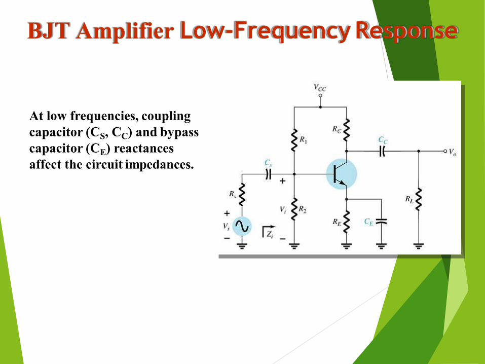
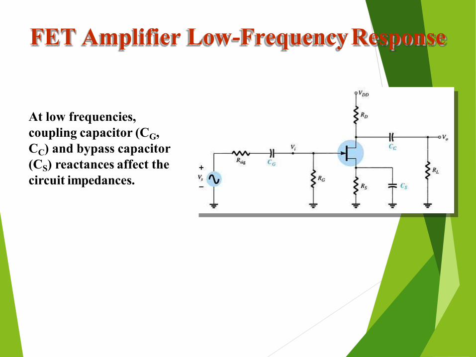
BJT Amplifier Low-Frequency Response
At low frequencies, coupling capacitor (CS, CC) and bypass capacitor (CE) reactances affect the circuit impedances.

Coupling Capacitor (CS)
The cutoff frequency due to CS can be calculated by
Ls1
2(Rs Ri )Csf
where
R i R 1 || R 2 || βre

L co
12π(R R )C
fLC
Coupling Capacitor (CC)
The cutoff frequency due to CC can be calculated with
where
Ro RC || ro

Bypass Capacitor (CE)
e E2πR C1
fLE
β
R Re RE || ( s re )
The cutoff frequency due to CE can be calculated with
where
and
Rs Rs || R1 || R2
BJT Amplifier Low-FrequencyResponse
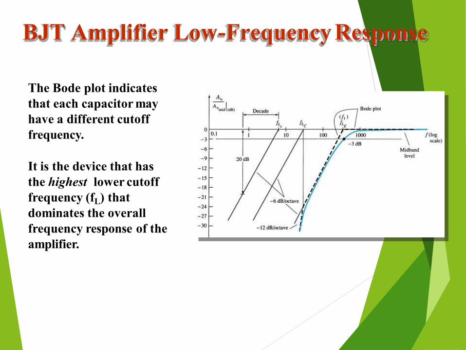
The Bode plot indicates that each capacitor may have a different cutoff frequency.
It is the device that has the highest lower cutoff frequency (fL) that dominates the overall frequency response of the amplifier.
Roll-Off of Gain in the Bode Plot
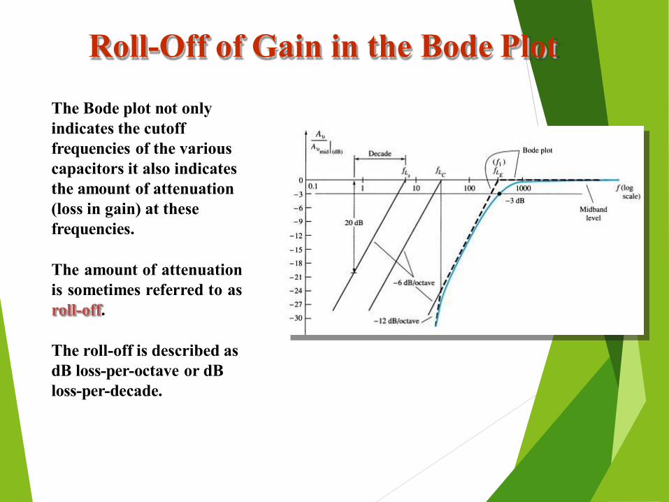
The Bode plot not only indicates the cutoff frequencies of the various capacitors it also indicates the amount of attenuation (loss in gain) at these frequencies.
The amount of attenuationis sometimes referred to asroll-off.
The roll-off is described as dB loss-per-octave or dB loss-per-decade.
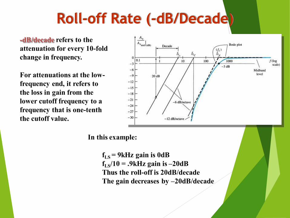
Roll-off Rate (-dB/Decade)
-dB/decade refers to the attenuation for every 10-fold change in frequency.
For attenuations at the low-frequency end, it refers to the loss in gain from the lower cutoff frequency to a frequency that is one-tenth the cutoff value.
In this example:
fLS = 9kHz gain is 0dB fLS/10 = .9kHz gain is –20dBThus the roll-off is 20dB/decadeThe gain decreases by –20dB/decade
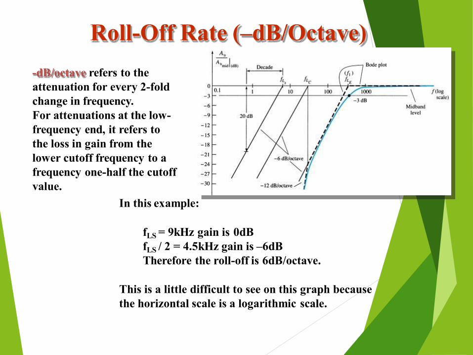
Roll-Off Rate (–dB/Octave)-dB/octave refers to the attenuation for every 2-fold change in frequency.For attenuations at the low-frequency end, it refers to the loss in gain from the lower cutoff frequency to a frequency one-half the cutoff value.
In this example:
fLS = 9kHz gain is 0dBfLS / 2 = 4.5kHz gain is –6dBTherefore the roll-off is 6dB/octave.
This is a little difficult to see on this graph becausethe horizontal scale is a logarithmic scale.
FET Amplifier Low-FrequencyResponse
At low frequencies, coupling capacitor (CG, CC) and bypass capacitor (CS) reactances affect the circuit impedances.
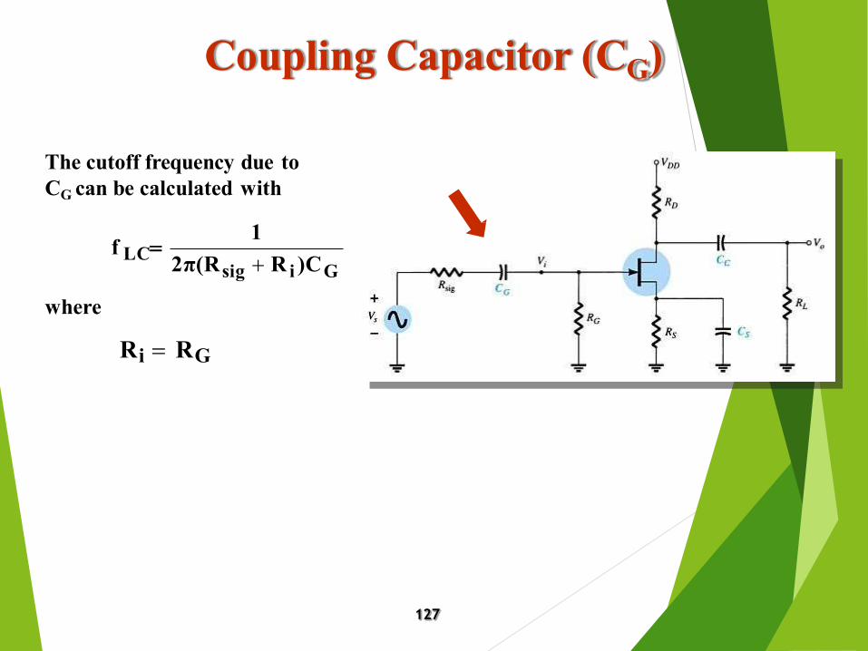
Coupling Capacitor (CG)
i GsigLC 2π(R
1 R )C
f
The cutoff frequency due toCG can be calculated with
where
Ri RG
127
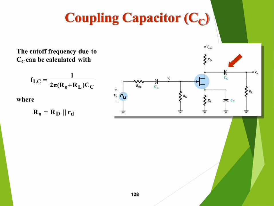
Coupling Capacitor (CC)
L Co
12π(R R )C
fLC
The cutoff frequency due toCC can be calculated with
where
Ro RD || rd
128

Bypass Capacitor (CS)
eq S2πR C1fLS
mSeq g
1rd ΩR R ||
The cutoff frequency due toCS can be calculated with
where
129
FET Amplifier Low-FrequencyResponse
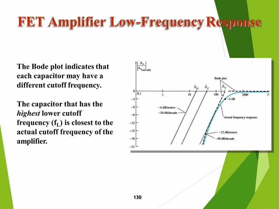
The Bode plot indicates that each capacitor may have a different cutoff frequency.
The capacitor that has the highest lower cutoff frequency (fL) is closest to the actual cutoff frequency of the amplifier.
130
Miller Capacitance
Any p-n junction can develop capacitance. In a BJT amplifier,this capacitance becomes noticeable across:
• The base-collector junction at high frequencies in common-emitter BJT amplifier configurations
• The gate-drain junction at high frequencies in common-source FET amplifier configurations.
These capacitances are represented as separate input and output capacitances, called the Miller Capacitances.
131

Miller Input Capacitance (CMi)
Note that the amount of Miller capacitance is dependent on inter-electrode capacitance from input to output (Cf) and the gain (Av).
CMi (1 Av )Cf
132
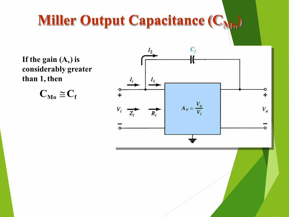
Miller Output Capacitance (CMo)
If the gain (Av) is considerably greater than 1, then
CMo Cf

BJT Amplifier High-Frequency Response
Capacitances that affect thehigh-frequency response are
• Junctioncapacitances Cbe, Cbc, Cce
• Wiring capacitancesCwi, Cwo
• Coupling capacitorsCS, CC
• Bypass capacitorCE

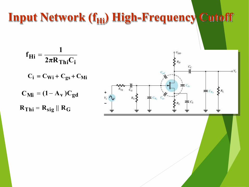
Input Network (fHi) High-Frequency Cutoff
Thi iHi 2πR C
1f
where
RThi Rs | | R1 || R2 || R i
andCi CWi Cbe CMi
CWi Cbe (1Av )Cbc

Output Network (fHo) High-FrequencyCutoff
Tho oHo 2πR C
1f
where
RTho RC || RL || ro
andCo CWo Cce CMo
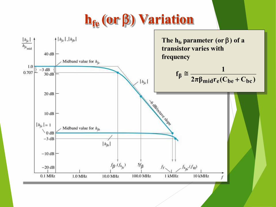
hfe (or ) VariationThe hfe parameter (or ) of a transistor varies with frequency
fβ 1
2πβmidre(Cbe Cbc )

BJT Amplifier FrequencyResponse
Note the highest lower cutoff frequency (fL) and the lowest upper cutofffrequency (fH) are closest to the actual response of the amplifier.
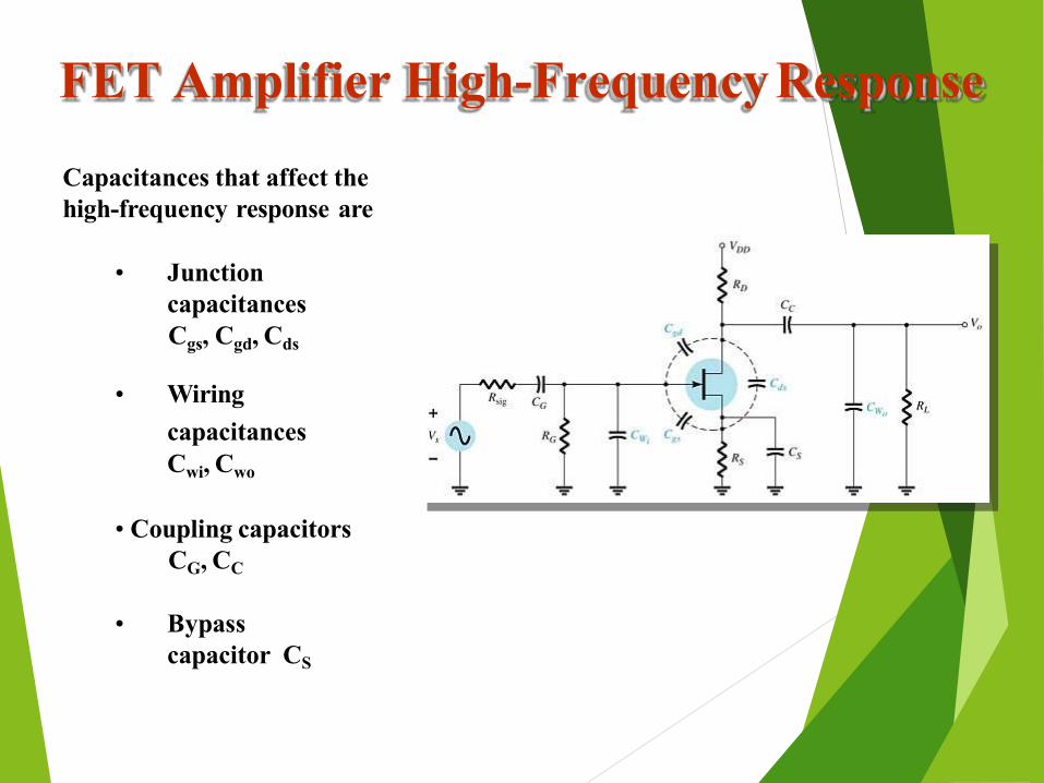
FET Amplifier High-FrequencyResponse
Capacitances that affect the high-frequency response are
• JunctioncapacitancesCgs, Cgd, Cds
• Wiring capacitances Cwi, Cwo
• Coupling capacitorsCG, CC
• Bypasscapacitor CS
Input Network (fHi) High-Frequency Cutoff
Thi iHi 2πR C
1f
RThi Rsig || RG
Ci CWi Cgs CMi
CMi (1 Av )Cgd

Output Network (fHo) High-Frequency Cutoff
Tho oHo 2πR C
1f
RTho RD || RL || rd
Co CWo Cds CMo
Mo A1
Cgd v
C 1

Multistage Frequency Effects
Each stage will have its own frequency response, but the output of one stage will be affected by capacitances in the subsequent stage. This is especially so when determining the high frequency response. For example, the output capacitance (Co) will be affected by the input Miller Capacitance (CMi) of the next stage.
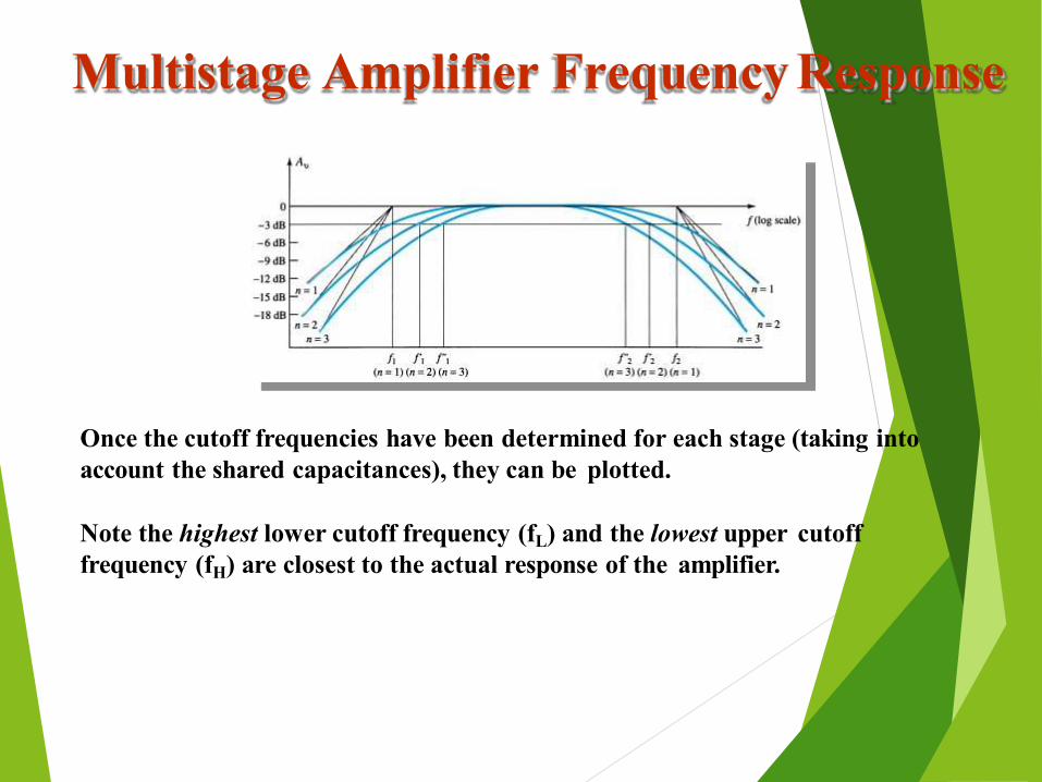
Multistage Amplifier Frequency Response
Once the cutoff frequencies have been determined for each stage (taking into account the shared capacitances), they can be plotted.
Note the highest lower cutoff frequency (fL) and the lowest upper cutofffrequency (fH) are closest to the actual response of the amplifier.
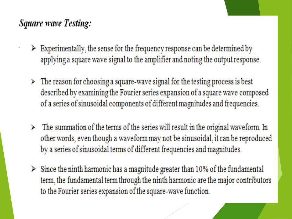
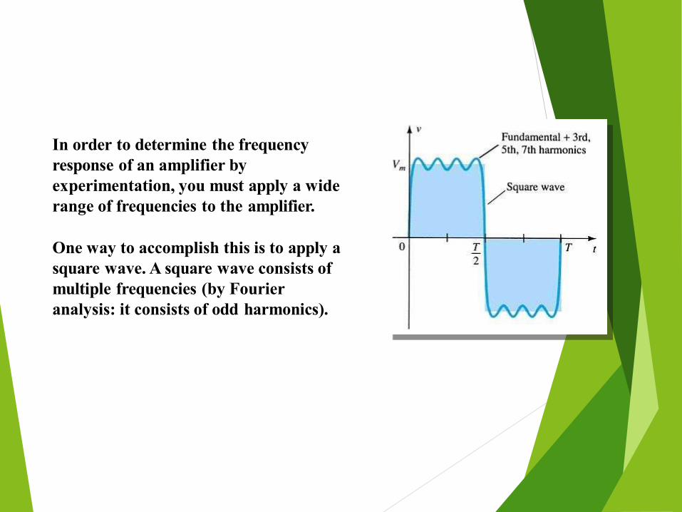
In order to determine the frequency response of an amplifier by experimentation, you must apply a wide range of frequencies to the amplifier.
One way to accomplish this is to apply a square wave. A square wave consists of multiple frequencies (by Fourier analysis: it consists of odd harmonics).
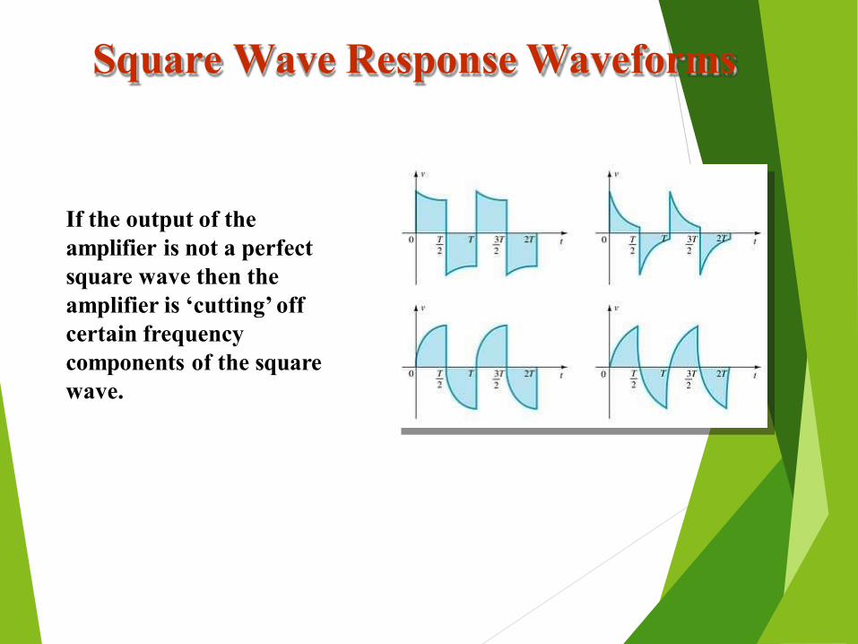
Square Wave Response Waveforms
If the output of the amplifier is not a perfect square wave then the amplifier is ‘cutting’ off certain frequency components of the square wave.

UNIT-III(a):
Multivibrators
147

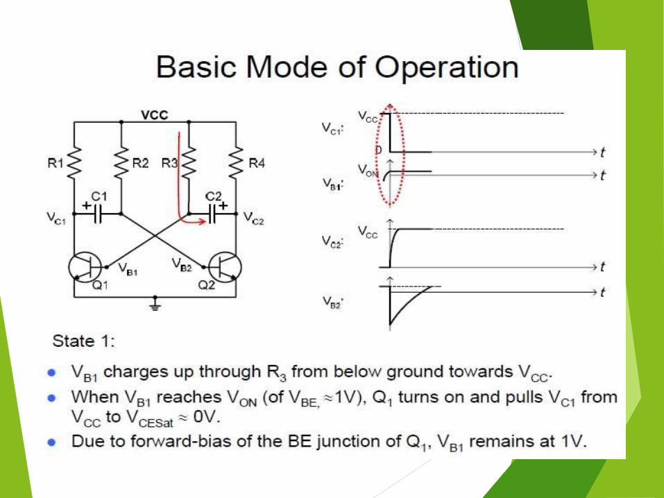
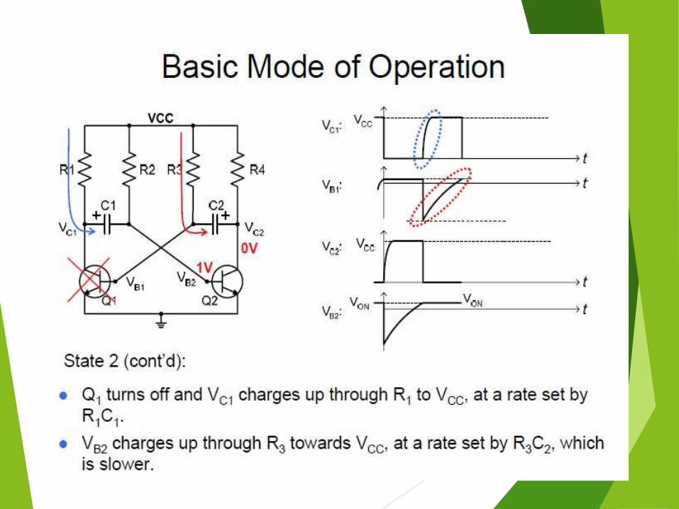
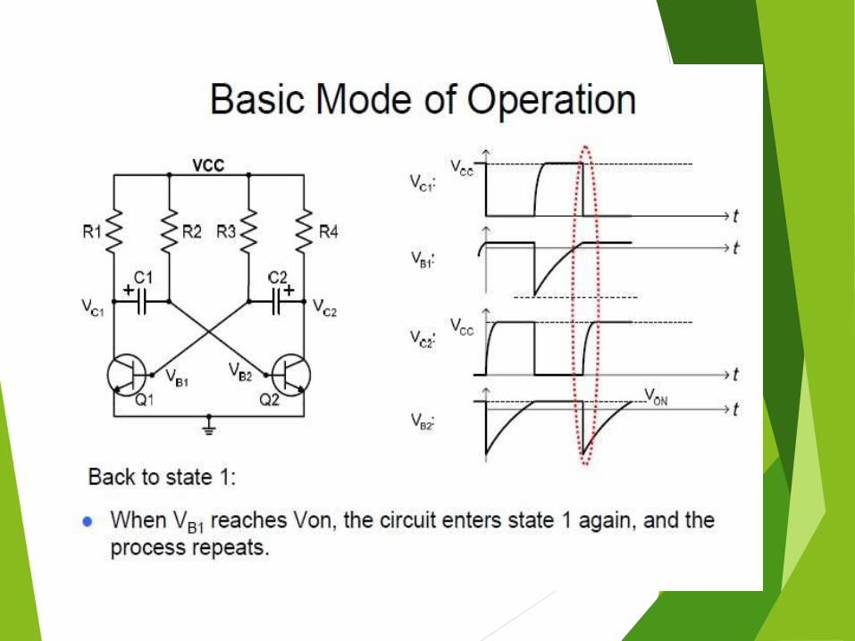
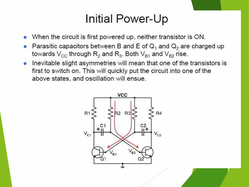
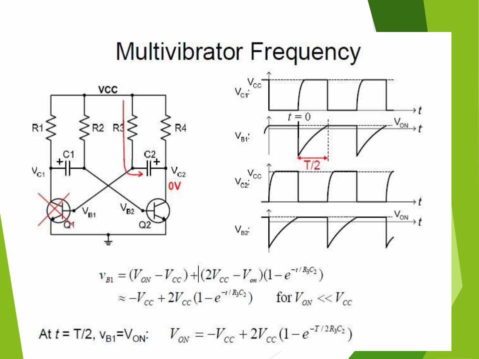
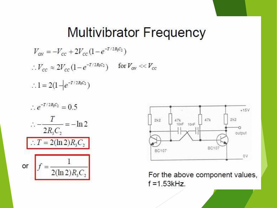
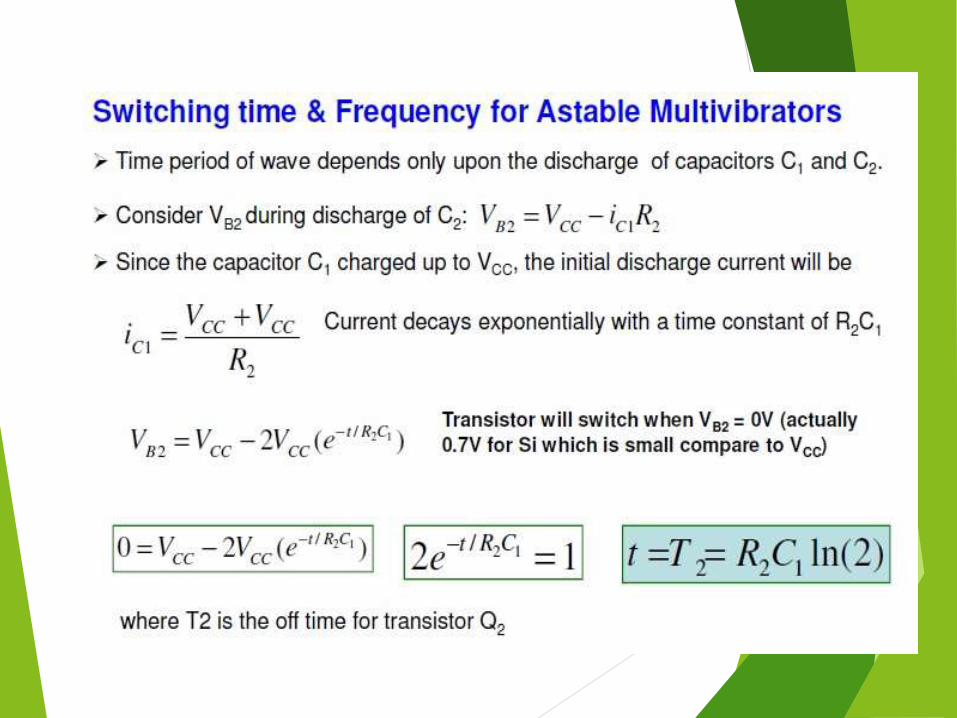
MULTIVIBRATORS A MULTIVIBRATOR is an electronic circuit that generates square, rectangular,
pulse waveforms, also called nonlinear oscillators or function generators.
Multivibrator is basically a two amplifier circuits arranged with regenerative
feedback.
There are three types of Multivibrator:
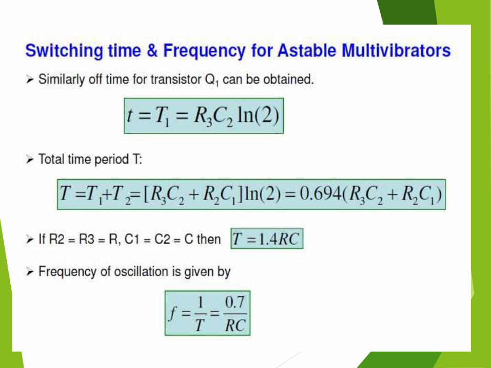
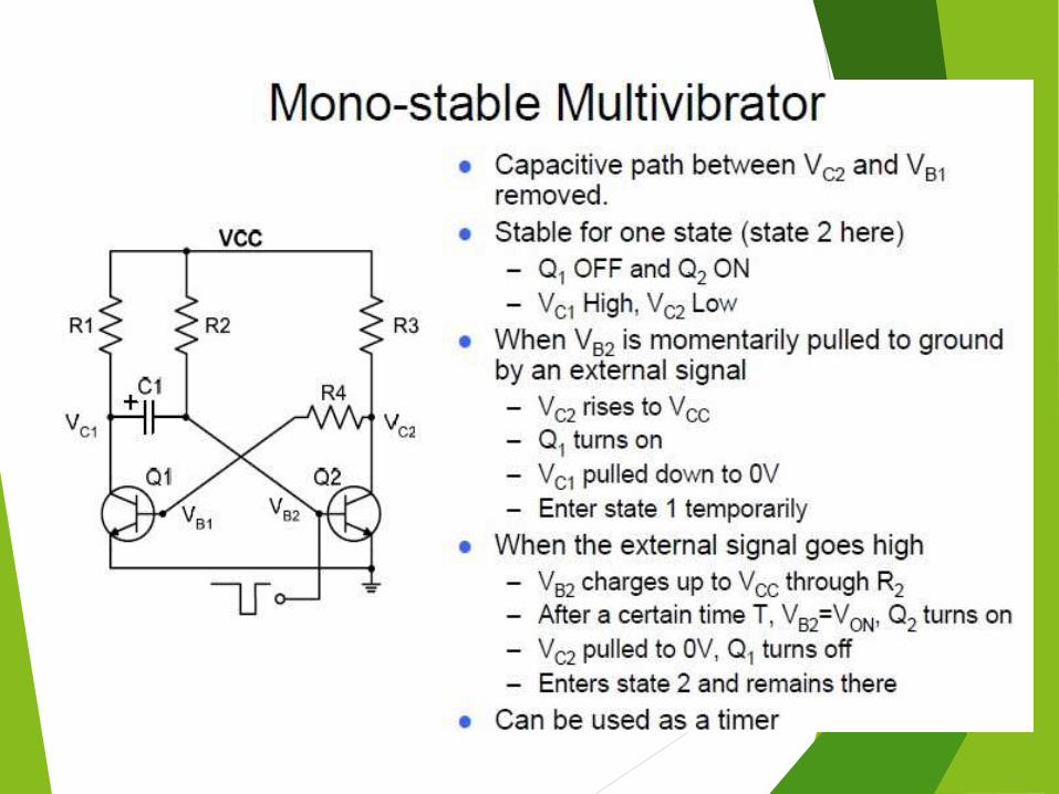
Astable Multivibrator: Circuit is not stable in either state—it continuously
Monostable Multivibrator: One of the state is stable but the other is not.
(Application in Timer)
Bistable Multivibrator: Circuit is stable in both the state and will remain in either
state indefinitely. The circuit can be flipped from one state to the other by an
external event or trigger. (Application in Flip flop)

MultivibratorsA multivibrator is used to implement simple two-state
systems such as oscillators, timers and flip-flops.Three types:
–Astable – neither state is stable.Applications: oscillator, etc.– Monostable - one of the states is stable, but the other is not;Applications: timer, etc.–Bistable – it remains in either state indefinitely. Applications: flip-flop, etc.


UNIT-3(b)CLIPPERS AND CLAMPERS

UNIT-3.BCLIPPERS AND CLAMPERS
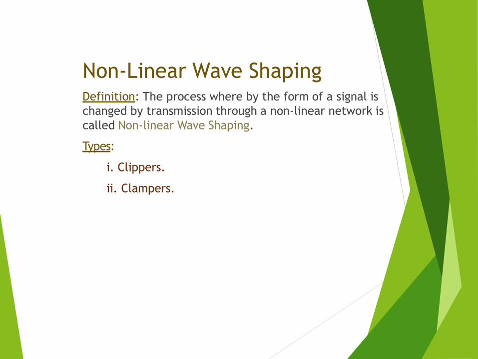
Non-Linear Wave ShapingDefinition: The process where by the form of a signal is
changed by transmission through a non-linear network is
called Non-linear Wave Shaping.
Types:
i. Clippers.
ii. Clampers.


Positive Shunt clipping with zero reference
voltage R
DVoVi
Transfer characteristics equations:
VO = 0 for Vi > 0
VO = Vi for Vi < 0
D – ONVO=Vγ for Vi > Vγ
VO=Vi for Vi < Vγ D – OFF
[Ideal]
VO
Vi
VO
Vi
Slope =1Vγ Vγ
Input
Output
Input

Positive Shunt clipping with positive
reference voltageR
Vi
D
Vo
Vi < VR+Vγ D – OFF VO
= Vi
D – ONVi > VR+Vγ
VO = VR+Vγ
VR + Vγ VR + Vγ
Input
Transfer characteristics equations:
Output
VOVR VO
Vi
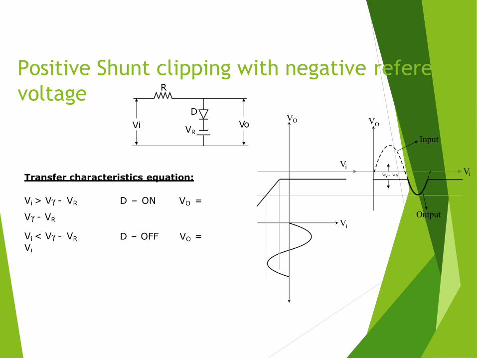
Positive Shunt clipping with negative reference
voltageR
D
VRVi Vo
Transfer characteristics equation:
Vi > Vγ - VR
Vγ - VR
D – ON VO =
Vi < Vγ - VR
Vi
D – OFF VO =
VO VO
Vi
Vi
Input
Output
Vi
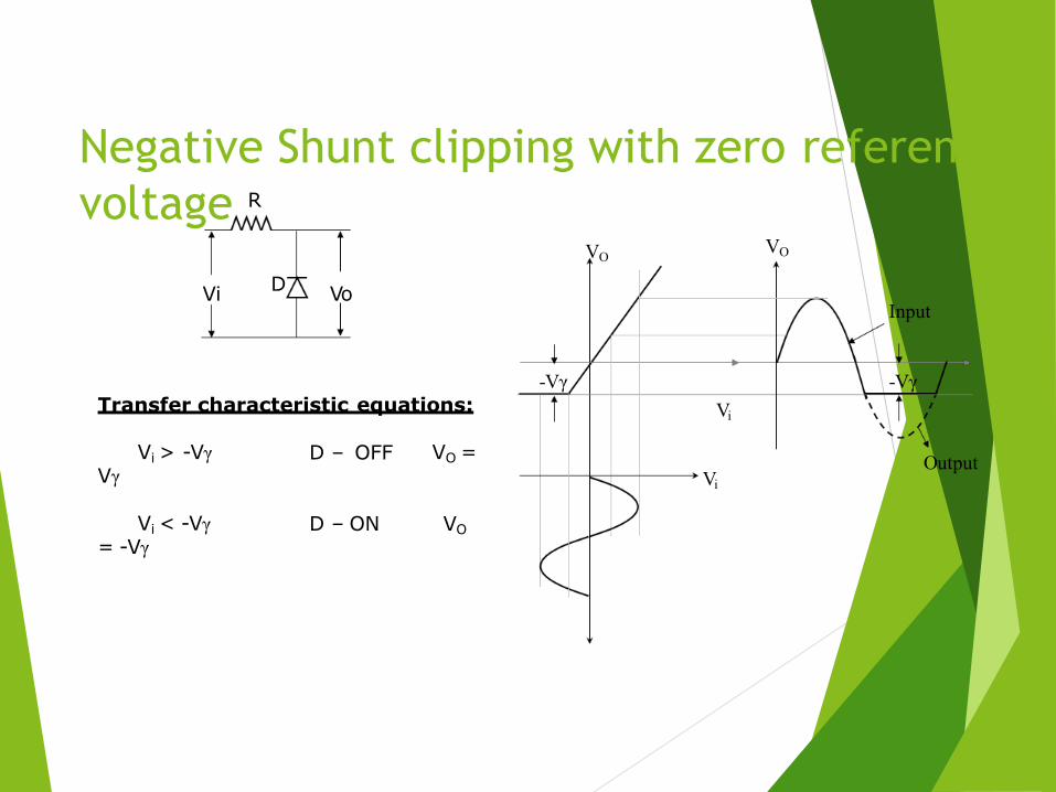
Negative Shunt clipping with zero reference
voltage R
Vi VoD
Transfer characteristic equations:
D – OFFVi > -Vγ VO =Vγ
D – ON VOVi < -Vγ
= -Vγ
-Vγ -Vγ
VO VO
Vi
Vi
Input
Output
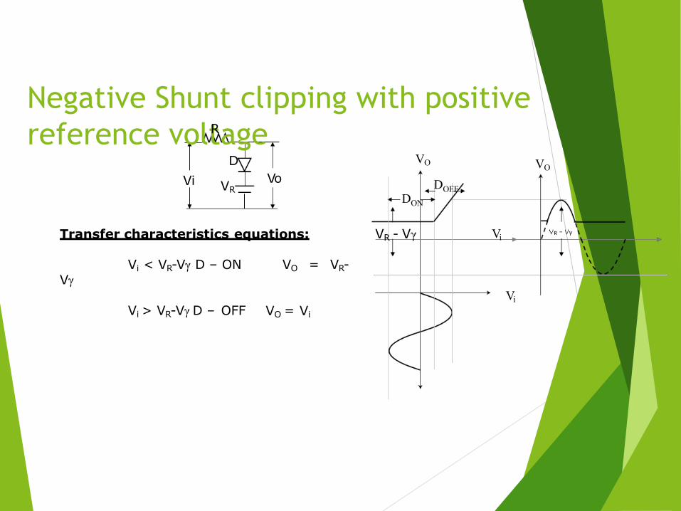
Negative Shunt clipping with positive
reference voltRageD
VRVi Vo
Transfer characteristics equations:
Vi < VR-Vγ D – ON VO = VR-Vγ
Vi > VR-Vγ D – OFF VO = Vi
VR - Vγ
VO VO
Vi
Vi
DON
DOFF
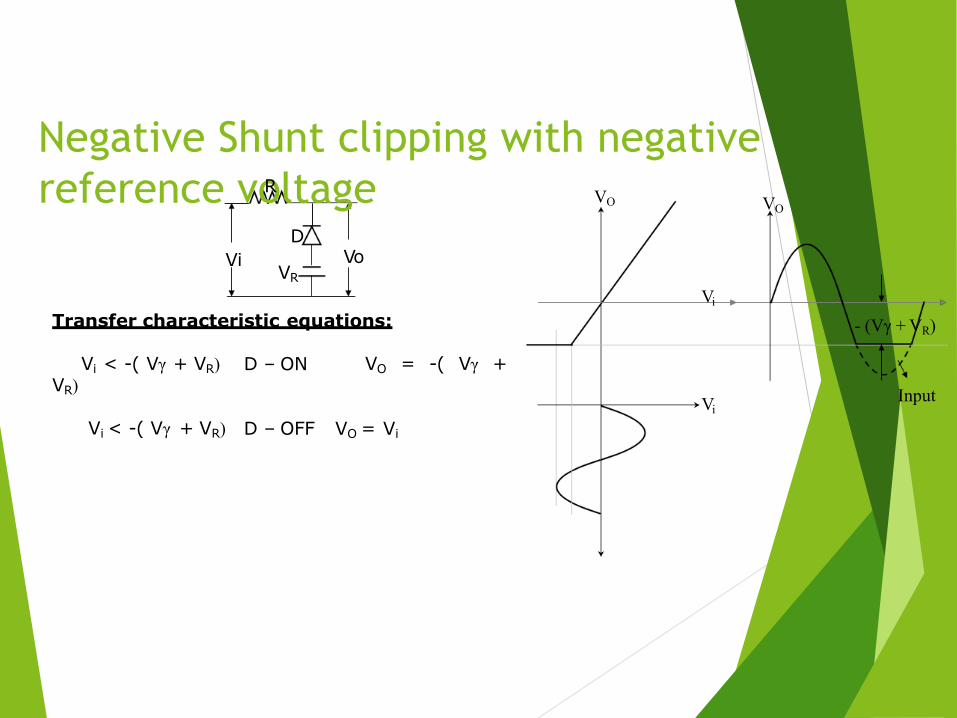
Negative Shunt clipping with negative
reference voR ltageD
VR
Vi Vo
Transfer characteristic equations:
D – ONVi < -( Vγ + VR) VO = -( Vγ +VR)
Vi < -( Vγ + VR) D – OFF VO = Vi
VO VO
Vi
Vi
- (Vγ + VR)
Input

RVi Vo
Negative Series clipper with zero referenceD
Transfer characteristic equations:
Vi<0 D –OFF VO = 0
Ideal DiodeVi>0 D –ON VO = Vi
Vi < Vγ D –OFF VO=0
Practical DiodeVi > Vγ D –ON VO=Vi - Vγ
VO VO
Vi
Vi
Output

CLIPPING ART TWO INDEPENDENT LEVELS
D
VR
Vi VoD
VR
Transfer characteristic equations:
Input
(Vi)Diode State
Output
(VO)
Vi VR1
D1 – ON, D2 – OFF VO = VR1
VR Vi VR1 2
D1 – OFF, D2 – OFF VO = Vi
Vi VR2D1 – OFF, D2 – ON VO = VR
2
VO VO
Vi
Vi
Input
OutputVR
1

CLAMPING CIRCUITThe need to establish the extremity of the positive (or) negative signal excursion at some reference level. When the signal is passed through a capacitive coupling network such a signal has lost its d.c. component. The clamping circuit introduces the d.c. components at the outside, for this reason the coupling circuits are referred to as d.c. restore (or) d.c. reinserter.
Def : “A clamping circuit is one that takes an input waveform and provides an output i.e., afaithful replica of its shape, but has one edge clamped to the zero voltage reference point.
There are two types of clampingcircuits.
1)
2)
Negative clampingcircuit.
Positive clampingcircuit.

Diode :- ClamperPositive Clamper
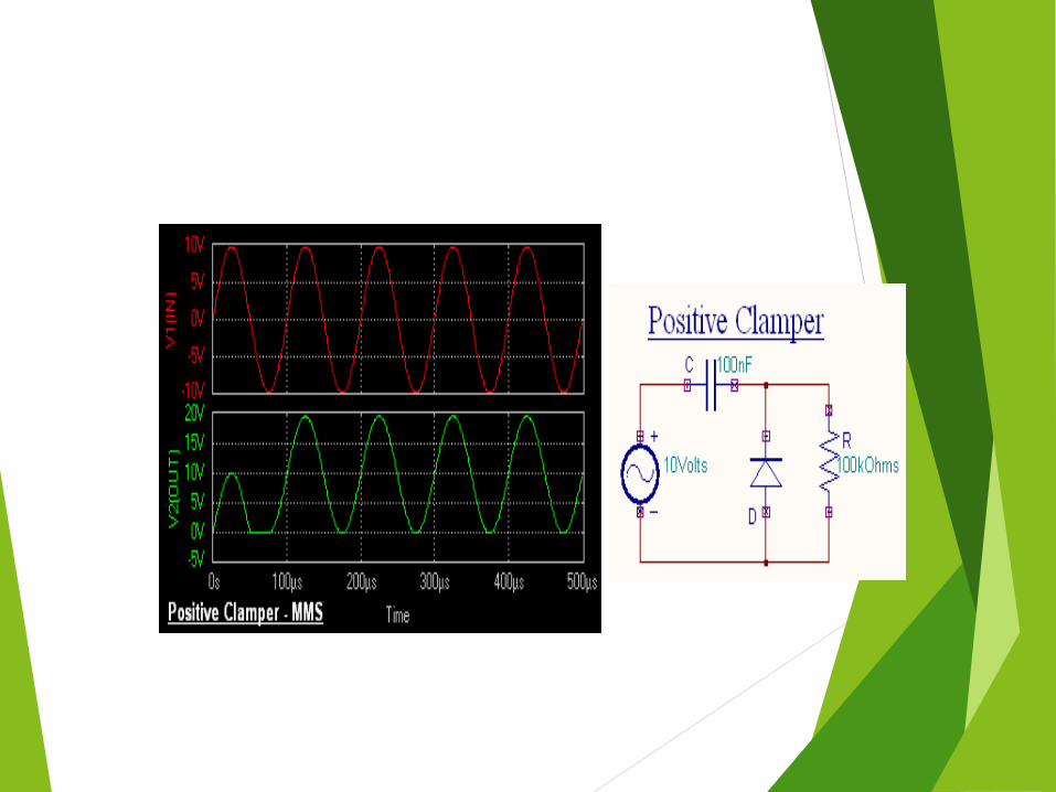
The circuit for a positive clamper is shown in the figure. During the negative half cycle of the input signal, the diode conducts and acts like ashort circuit.The output voltage Vo0 volts. The capacitor is charged to the peak value of input voltage Vm. and it behaves like a battery. Duringthepositive half of the input signal, the diode does not conduct and acts as an open circuit. Hence the outputvoltageVo Vm+ Vm This gives a positively clampedvoltage.
Vo Vm+ Vm = 2 Vm
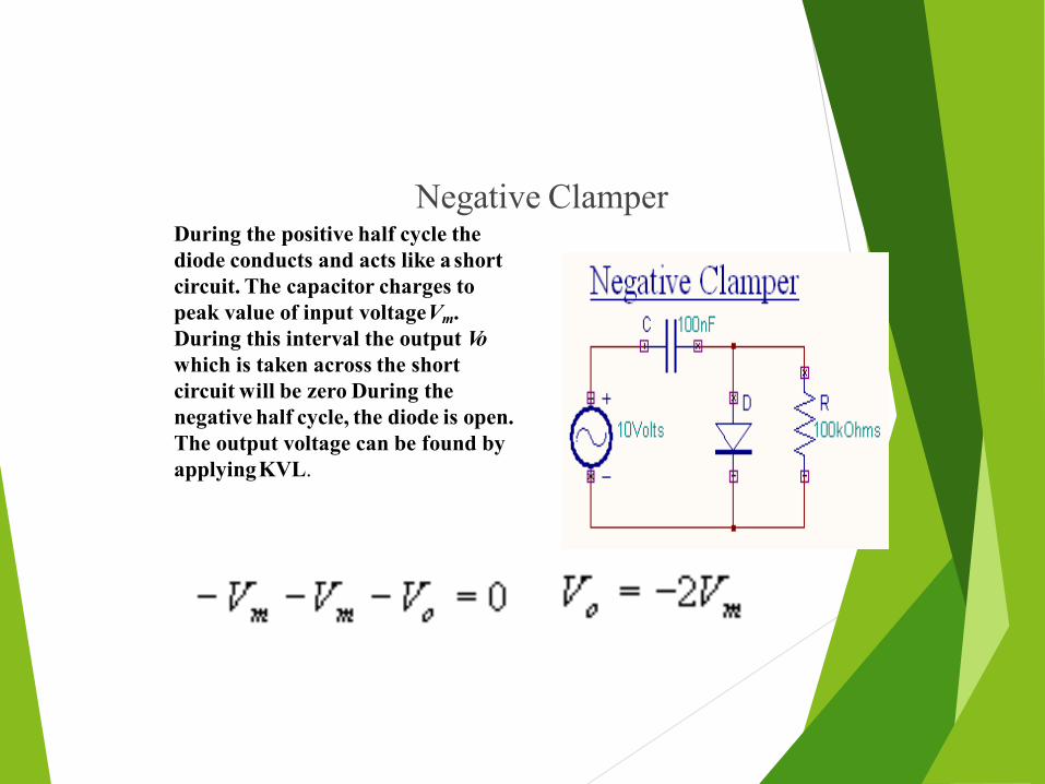
Negative ClamperDuring the positive half cycle the diode conducts and acts like a short circuit. The capacitor charges to peak value of input voltageVm.During this interval the output Vo which is taken across the short circuit will be zero During the negative half cycle, the diode is open. The output voltage can be found by applyingKVL.


Biased Clamper
CLAMPING CIRCUIT THEOREM
Therefore the charge acquired by the capacitor during the forward interval
Af = RfAr R
Consider a square wave input is applied to a clamping circuit under steady state condition
If Vf (t) is the output waveform in the forward direction, then from below figure the capacitor
charging current is
f
Vfif =R
Therefore the charge acquired by the capacitor during the forward intervalT1 T1
f f
Af1 V dt =R R if dt =
0
f
0
…………….. (1)

Similarly if Vf (t) is the output voltage in the reverse direction,then the current which discharges by the capacitor is
T21ir dt = Vr dt =
Ar R
T2
T1
R T2
…………….. (2)
In the steady-state the net charge acquired by the capacitor must be zero.
Therefore from equation (1) & (2) this equation says that for any
input waveform the ratio of the area under the output voltage curve in the
forward direction to the reverse direction is equal to the ratio .


Unit-4(a)Large Signal Amplifiers

Power Amplifier (ClassA)
Induction of PowerAmplifier
Power and Efficiency
Amplifier Classification
Basic Class AAmplifier
Transformer Coupled Class AAmplifier
Push pull amplifier
Complementary Symmetry circuits
Phase inverters

Power amplifiers are used to deliver a relatively high amountof power, usually to a low resistance load.
Typical load values range from 300W (for transmissionantennas) to 8W (for audio speaker).
Although these load values do not cover every possibility, theydo illustrate the fact that power amplifiers usually drive low-resistance loads.
Typical output power rating of a power amplifier will be 1W or higher.
Ideal power amplifier will deliver 100% of the power it draws from the supply to load. In practice, this can never occur.
The reason for this is the fact that the components in the amplifier will all dissipate some of the power that is being drawn form the supply.

Amplifier Power Dissipation
2
2
ICQRC
RE
P1 = I1 R1 R1
P2 = I2 R2 R2
VCC
I1
I2
ICC
CP = I2 RCQ C
2PT = ITQRT
2PE = IEQR E
IEQ
The total amount of power being dissipated by the amplifier, Ptot , is
Ptot = P1 + P2 + PC + PT + PE
The difference between this total value and the total power being drawn from the supply is the power that actually goes to the load – i.e. output power.
Amplifier Efficiency

Amplifier Efficiency
A figure of merit for the power amplifier is its efficiency, .
Efficiency ( of an amplifier is defined as the ratio of acoutput power (power delivered to load) to dc input power .
By formula :
As we will see, certain amplifier configurations have muchhigher efficiency ratings than others.
This is primary consideration when deciding which type ofpower amplifier to use for a specific application.
Amplifier Classifications
dc input power P(dc)i
power100%
Po (ac)100%
ac output
Amplifier Classifications
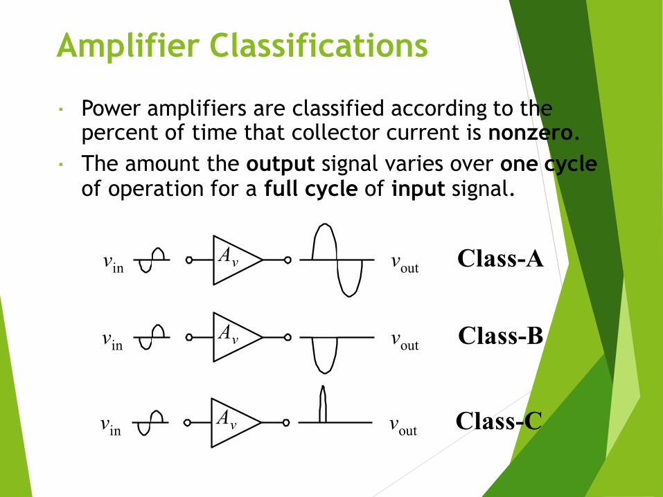
Power amplifiers are classified according to the percent of time that collector current is nonzero.
The amount the output signal varies over one cycleof operation for a full cycle of input signal.
vin voutAv Class-A
vin voutAv Class-B
vin voutAv Class-C

Efficiency Ratings
The maximum theoretical efficiency ratings of class-A, B, and C
amplifiers are:
Amplifier Maximum TheoreticalEfficiency, max
ClassA 25%
Class B 78.5%
Class C 99%

Class AAmplifier
output waveform same shape input waveform + phase shift.
The collector current is nonzero 100% of the time.
inefficient, since even with zero input signal, ICQ
is nonzero
(i.e. transistor dissipates power in the rest, orquiescent, condition)
vin voutAv
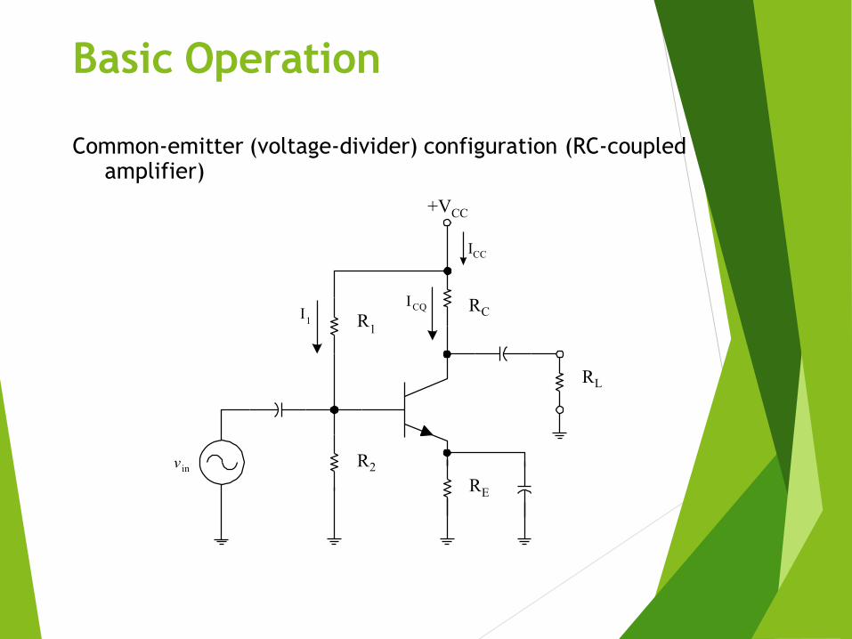
Basic Operation
RC
RE
R1
R2
RL
v in
ICQI1
Common-emitter (voltage-divider) configuration (RC-coupledamplifier)
+VCC
ICC
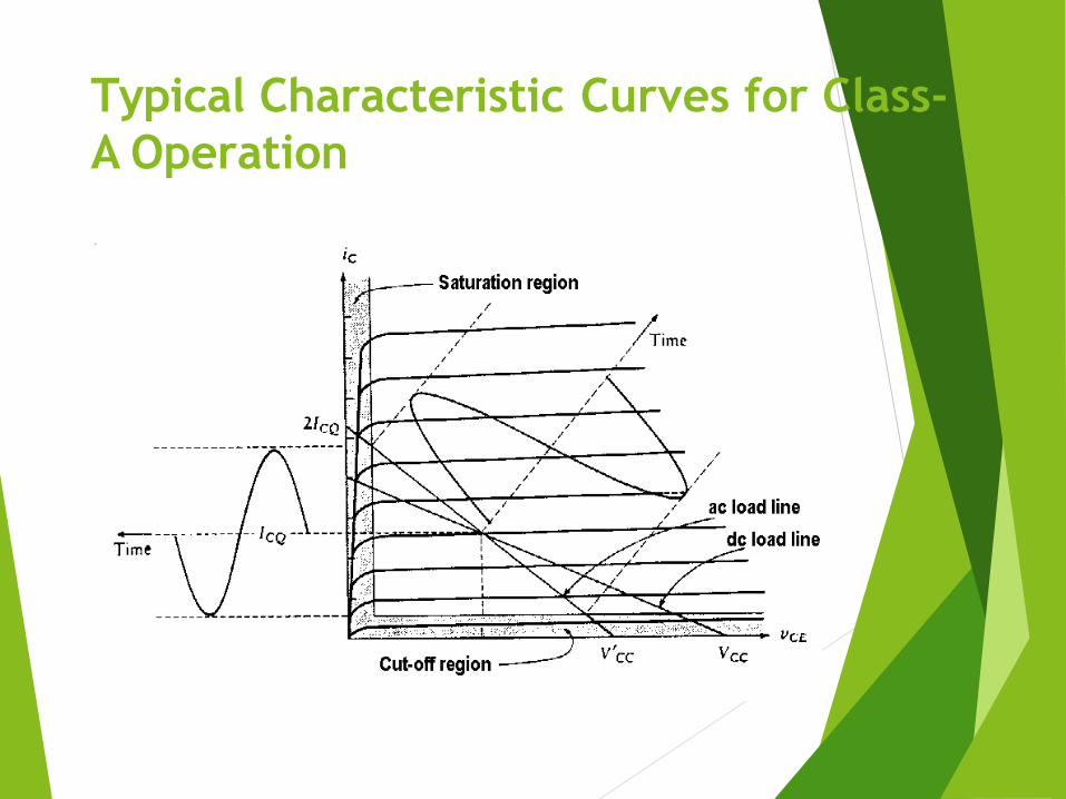
Typical Characteristic Curves for Class-
A Operation

Typical Characteristic
Previous figure shows an example of a sinusoidal input and the
resulting collector current at the output.
The current, ICQ , is usually set to be in the center of the ac load line.
Why?
(DC and AC analyses discussed in previous
sessions)
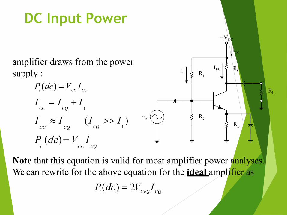
DC Input Power
RC
RE
R1
R2
RL
v in
ICQI1
+VCC
ICC
amplifier draws from the powersupply :
CC CCiP (dc) V I
I I ICC CQ 1
I ICC CQ
(I I )CQ 1
P (dc)V Ii CC CQ
Note that this equation is valid for most amplifier power analyses.We can rewrite for the above equation for the ideal amplifier as
CEQ CQiP(dc) 2V I
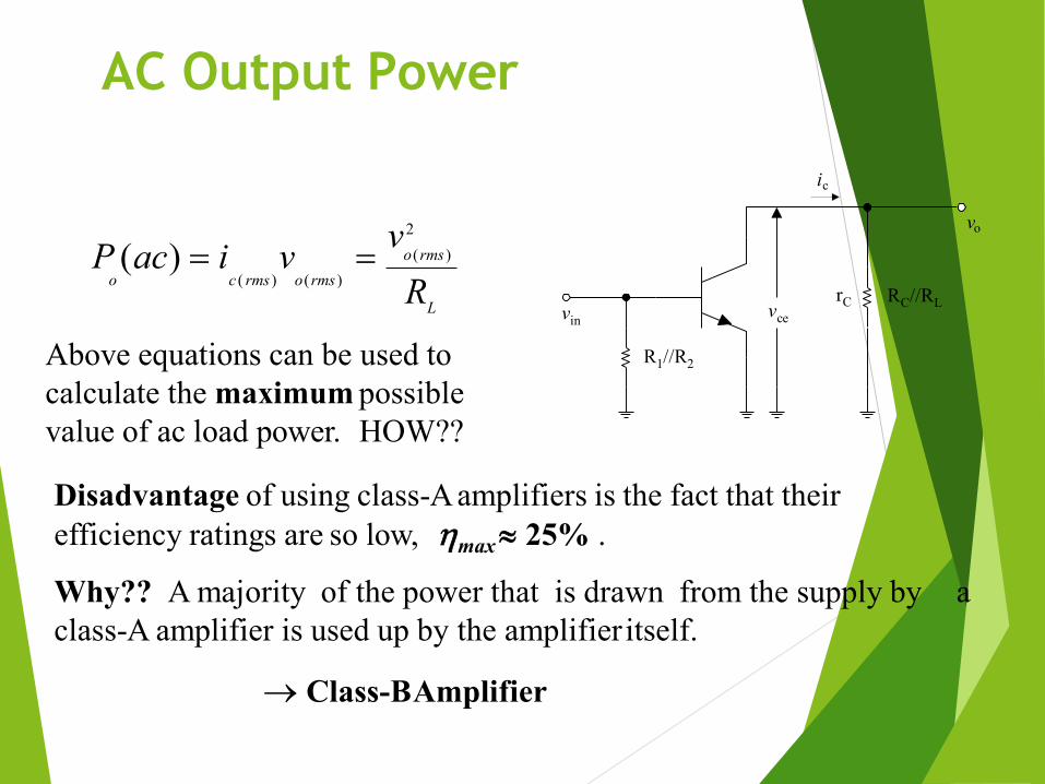
AC Output Power
R1//R2
vcevin
vo
ic
rC RC//RL
Above equations can be used to calculate the maximum possible value of ac load power. HOW??
LRv 2
o(rms )P (ac) i v o c ( rms ) o(rms )
Disadvantage of using class-A amplifiers is the fact that theirefficiency ratings are so low, max 25% .
Why?? A majority of the power that is drawn from the supply by aclass-A amplifier is used up by the amplifier itself.
Class-BAmplifier
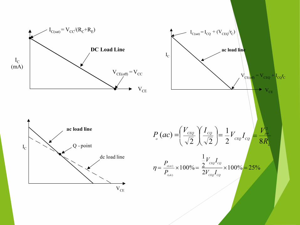
IC (mA)
VCE
VCE(off) = VCC
IC(sat) = VCC/(RC+RE)
DC Load LineIC
VCE
IC(sat) = ICQ CEQ C+ (V /r )
V = V + I rCE(off) CEQ CQ C
ac load line
IC
VCE
Q - point
ac load line
dc load line
L
PPCEQ CQo
V8R22 2
2
I CEQ CQ
I 1VVP (ac)
2 100% 25%100% CEQ CQ
CEQ CQ
i (dc)
o(ac)
2V I
I1V
PP
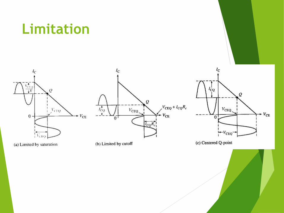
Limitation
Example
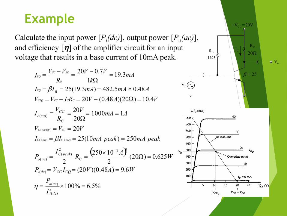
Calculate the input power [Pi(dc)], output power [Po(ac)],and efficiency [] of the amplifier circuit for an input voltage that results in a base current of 10mA peak.
+VCC = 20V
IC
Vi
25
RC
20RB
1kVo
2 2C
2C( peak)
o(ac)
Cc(sat)
B
(20) 0.625W250103 A2R I
P
20V
1000mA 1AR 20
VCCI
VCEQ VCC ICRC 20V (0.48A)(20) 10.4V
VCC VBE
20V 0.7V
19.3mARB 1k
IBQ
Pi (dc) VCC ICQ (20V )(0.48A) 9.6W P
o(ac) 100% 6.5%Pi(dc)
VCE (cutoff ) VCC 20VIC ( peak) Ib( peak) 25(10mA peak ) 250mA peak
ICQ I 25(19.3mA) 482.5mA 0.48A
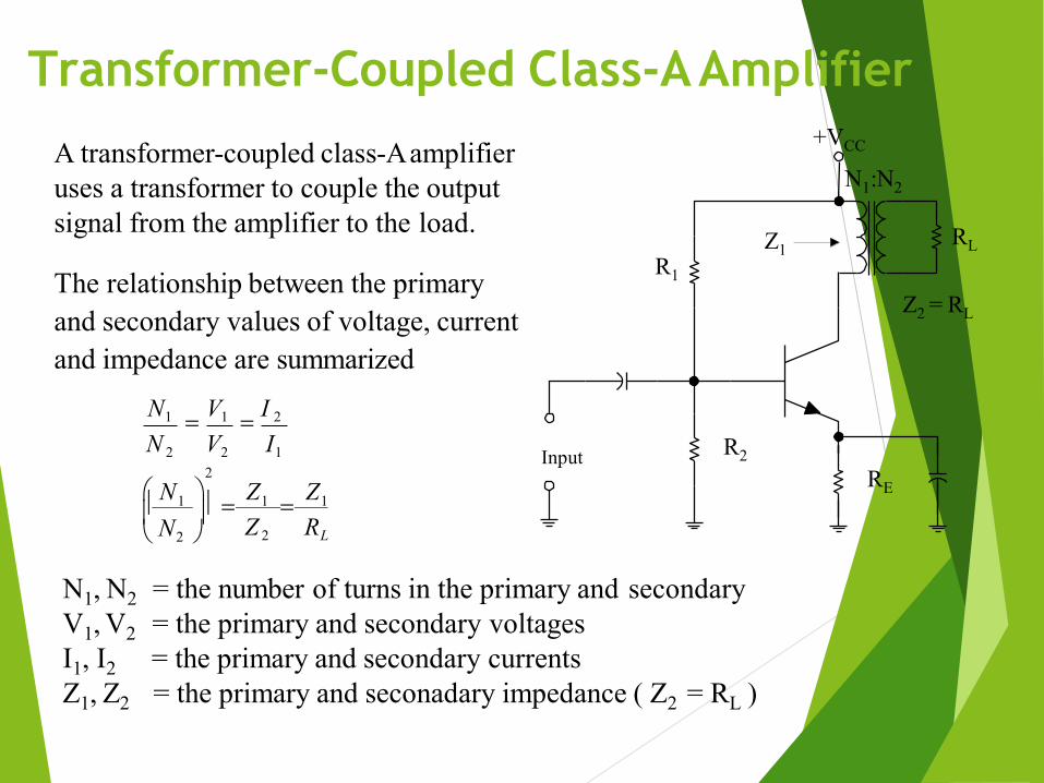
Transformer-Coupled Class-AAmplifier
InputRE
R1
R2
RL
+VCC
N1:N2
Z2 = RL
Z1
A transformer-coupled class-Aamplifier uses a transformer to couple the output signal from the amplifier to the load.
Z 2 RL
1 1 1
N2
2 N Z Z
The relationship between the primary and secondary values of voltage, current and impedance are summarized
N1 V1
I 2
N 2 V2 I1
N1, N2 V1, V2 I1, I2 Z1, Z2
= the number of turns in the primary and secondary= the primary and secondary voltages= the primary and secondary currents= the primary and seconadary impedance ( Z2 = RL )
Transformer-Coupled Class-AAmplifier
An important characteristic of the transformer is the ability to produce acounter emf, or kick emf.
When an inductor experiences a rapid change in supply voltage, it will produce a voltage with a polarity that is opposite to the original voltage polarity.
The counter emf is caused by the electromagnetic field that surrounds theinductor.
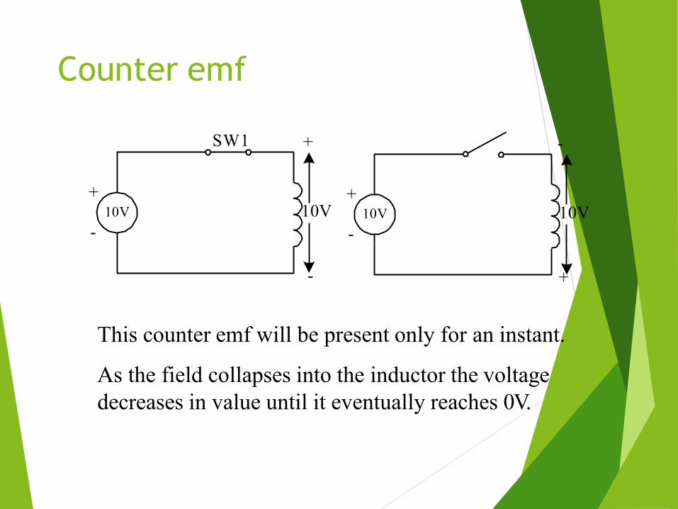
Counter emf
10V+
-
+
-
10V
SW1
10V+
-
+
-
10V
This counter emf will be present only for an instant.
As the field collapses into the inductor the voltage decreases in value until it eventually reaches 0V.
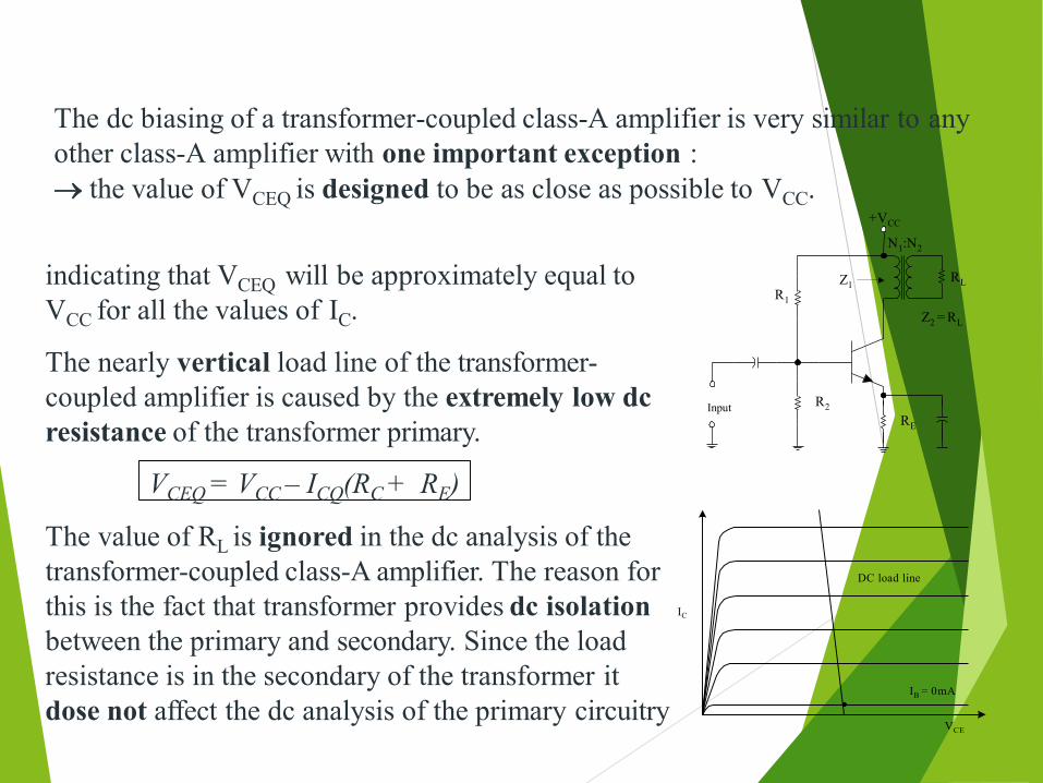
The dc biasing of a transformer-coupled class-A amplifier is very similar to anyother class-A amplifier with one important exception :
InputRE
R1
R2
RL
the value of VCEQ is designed to be as close as possible to VCC.+VCC
N1:N2
Z2 = RL
Z1
VCE
IB = 0mA
DC load line
indicating that VCEQ will be approximately equal toVCC for all the values of IC.
The nearly vertical load line of the transformer-coupled amplifier is caused by the extremely low dc resistance of the transformer primary.
VCEQ = VCC – ICQ(RC + RE)
The value of RL is ignored in the dc analysis of the transformer-coupled class-A amplifier. The reason for this is the fact that transformer provides dc isolation IC
between the primary and secondary. Since the load resistance is in the secondary of the transformer itdose not affect the dc analysis of the primary circuitry.
InputRE
R1
R2
RL
+VCC
N1:N2
Z2 = RL
Z1
VCE
IC
IB = 0mA
DC load line
ac load line
IC(max) = ??
~ VCEQ ~ VCC ~ 2VCC
Q-point
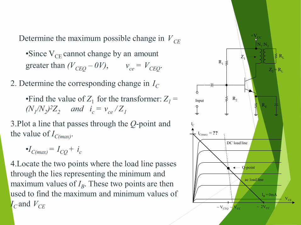
Determine the maximum possible change in V CE
•Since VCE cannot change by an amountgreater than (V – 0V),CEQ ce CEQv = V .
2. Determine the corresponding change in IC
•Find the value of Z1 for the transformer: Z1 =(N /N )2Z and i = v / Z1 2 2 c ce 1
3.Plot a line that passes through the Q-point andthe value of IC(max).
•IC(max) = ICQ + ic
4.Locate the two points where the load line passes through the lies representing the minimum and maximum values of IB. These two points are then used to find the maximum and minimum values of IC and VCE

212
InputRE
R1
R2
RL
+VCC
N1:N2
Z2 = RL
Z1
R1//R2
vcevin
Z1 vo
VCE
IC
ac load lineic
IB = 0mA
IC(max) = ??
DC load line
CEQ~ V ~ V CC ~ 2V CC
Q-pointICQ

Maximum load power and efficiency
The Power Supply for the amplifier : PS = VCCICC
Maximum peak-to-peak voltage across the primary of the transformer is approximately equal to the difference between the values ofVCE(max)and VCE(min) : VPP = VCE(max) – V•CE(min)
Maximum possible peak-to-peak load voltageis found by V(P-P)max = (N2 / N1)V PP
The actual efficiency rating of a transformer-coupled class-Aamplifier will generally be less than 40%.
N1 : N2
RLVPP V(P-P) max
There are several reasons for the difference between the practical and theoretical efficiency ratings for the amplifier :
1.
2.
The derivation of the = 50% value assumes that VCEQ = VCC . Inpractice, VCEQ will always be some value that is less the VCC .
The transformer is subject to various power losses. Among these losses are couple loss and hysteresis loss. These transformer power losses are not considered in the derivation of the = 50% value.

One of the primary advantages of using the
transformer-coupled class-A amplifier is the
increased efficiency over the RC-coupled
class-Acircuit.
Another advantage is the fact that the
transformer-coupled amplifier is easily
converted into a type of amplifier that is
used extensively in communications :- the
tuned amplifier.
A tuned amplifier is a circuit that is designed
to have a specific value of power gain over a
specific range of frequency.
B Amplifier
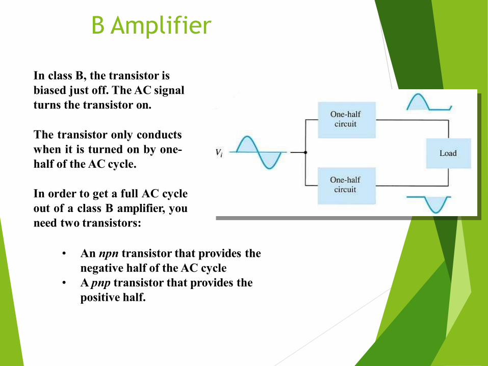
In class B, the transistor is biased just off. The AC signal turns the transistor on.
The transistor only conductswhen it is turned on by one-half of the AC cycle.
In order to get a full AC cycleout of a class B amplifier, youneed two transistors:
• An npn transistor that provides the negative half of the AC cycle
• A pnp transistor that provides thepositive half.
Class B Amplifier
Since one part of the circuit pushes the signal high
during one half-cycle and the other part pulls the signal
low during the other half cycle, the circuit is referred to
as a push-pull circuit
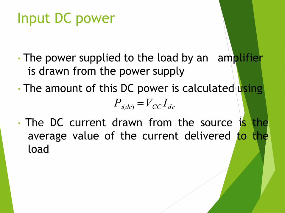
Input DC power
The power supplied to the load by an amplifier
is drawn from the power supply
The amount of this DC power is calculated using
Pi(dc) VCC Idc
The DC current drawn from the source is the
average value of the current delivered to the
load

Input DC power
The current drawn from a single DC supply has the
form of a full wave rectified signal, while that
drawn from two power supplies has the form of
half-wave rectified signal from each supply
On either case the average value for the current is
given by Idc I p
2
2The input power can be written as
Pi(dc) VCC Ip
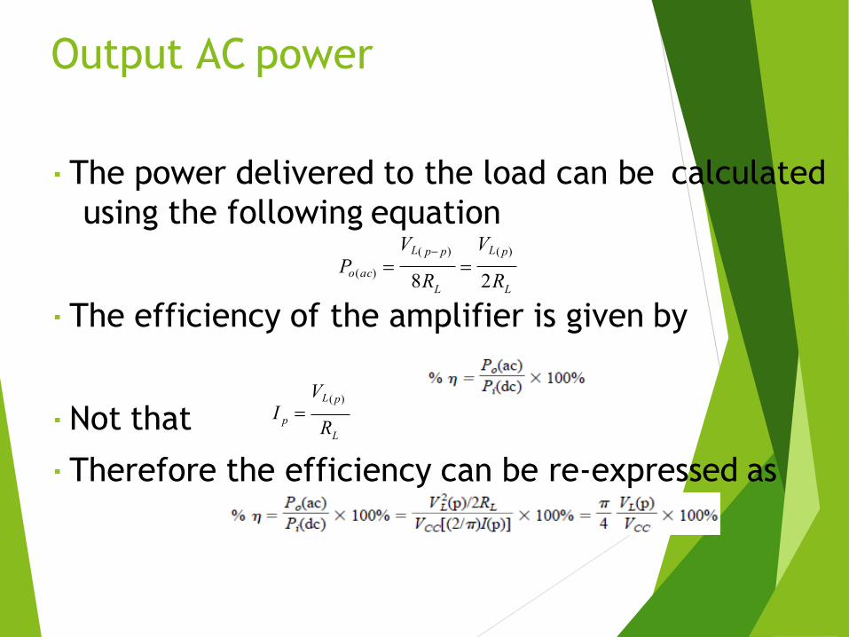
Output AC power
The power delivered to the load can be calculated
using the following equation
The efficiency of the amplifier is given by
Not that
Therefore the efficiency can be re-expressed as
L L8R 2Ro(ac)
VL( p p) VL( p)P
Lp R
VL( p)I
Output AC power
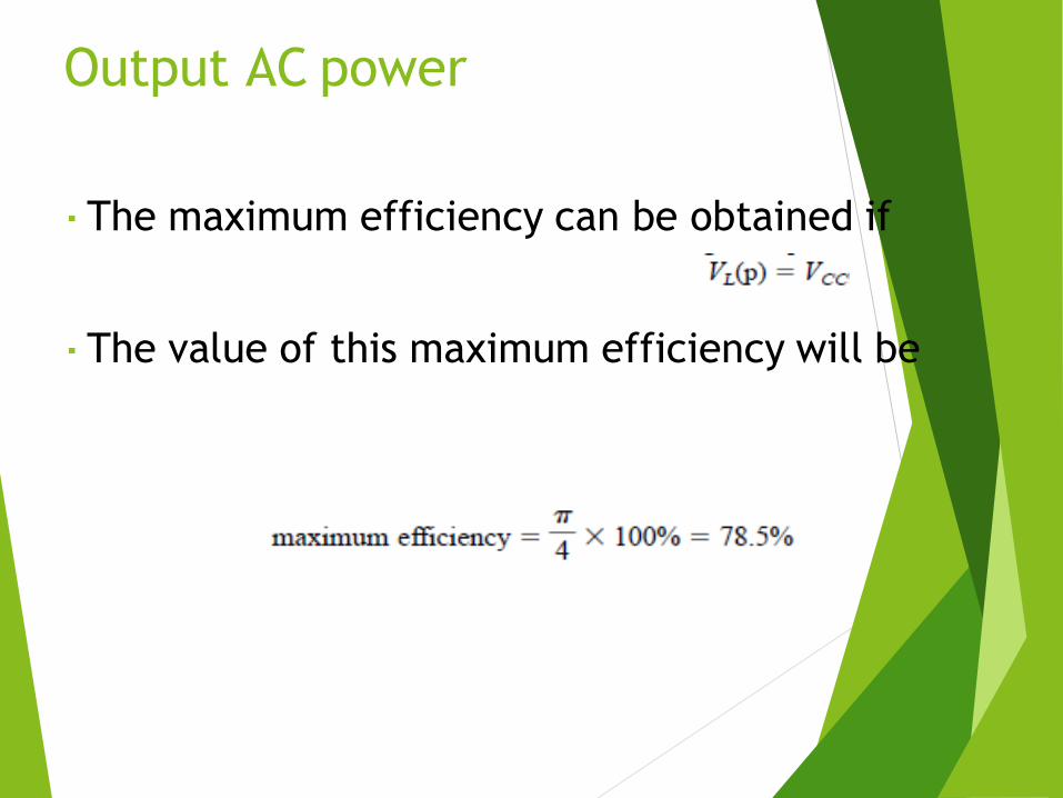
The maximum efficiency can be obtained if
The value of this maximum efficiency will be

Power dissipated by the output
transistors
The power dissipated by the output transistors as
heat is given by
The power in each transistor is given by
Example
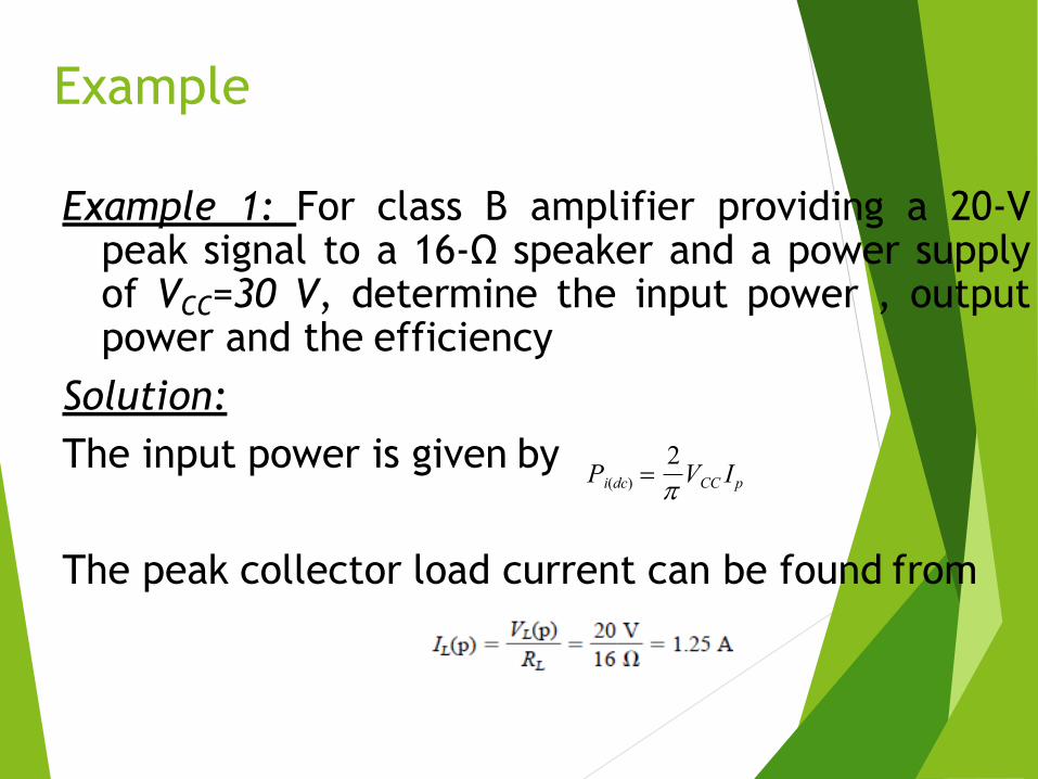
Example 1: For class B amplifier providing a 20-Vpeak signal to a 16-Ω speaker and a power supplyof VCC=30 V, determine the input power , outputpower and the efficiency
Solution:
The input power is given by
The peak collector load current can be found from
2Pi(dc)
VCC Ip

Example
Solution:
The input power is
The output power is given by
The efficiency is
i (dc)P
2 30(1.25) 23.9 W
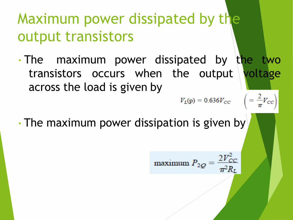
Maximum power dissipated by the
output transistors
The maximum power dissipated by the two
voltagetransistors occurs when the output
across the load is given by
The maximum power dissipation is given by
Example
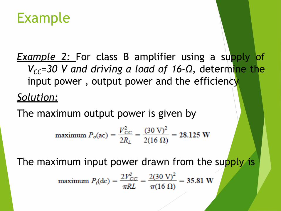
Example 2: For class B amplifier using a supply of
VCC=30 V and driving a load of 16-Ω, determine the
input power , output power and the efficiency
Solution:
The maximum output power is given by
The maximum input power drawn from the supply is
Example
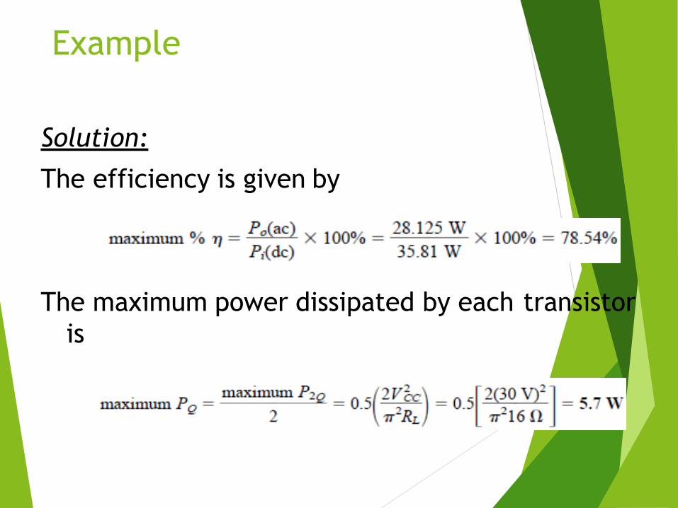
Solution:
The efficiency is given by
The maximum power dissipated by each transistor
is
Class B Amplifier circuits
A number of circuit arrangements canbe used to realize class B amplifier
We will consider in this course twoarrangements in particular
1. The first arrangement uses a single inputsignal fed to the input of twocomplementary transistors (complementarysymmetry circuits)
2. The second arrangement uses two out ofphase input signals of equal amplitudesfeeded to the input of two similar NPN orPNP transistors (quasi-complementary push-pull amplifier)

Complementary symmetry circuits
first arrangement
This circuit uses both npn and pnp transistor to construct class B amplifier as shown to the left
One disadvantage of this circuit is the need for two separate voltage supplies

Complementary symmetry circuits
circuit is theanother disadvantage of this resulting cross over distortion
Cross over distortion can be eliminated the bybiasing the transistors in class AB operationwhere the transistors are biased to be on forslightly more than half a cycle
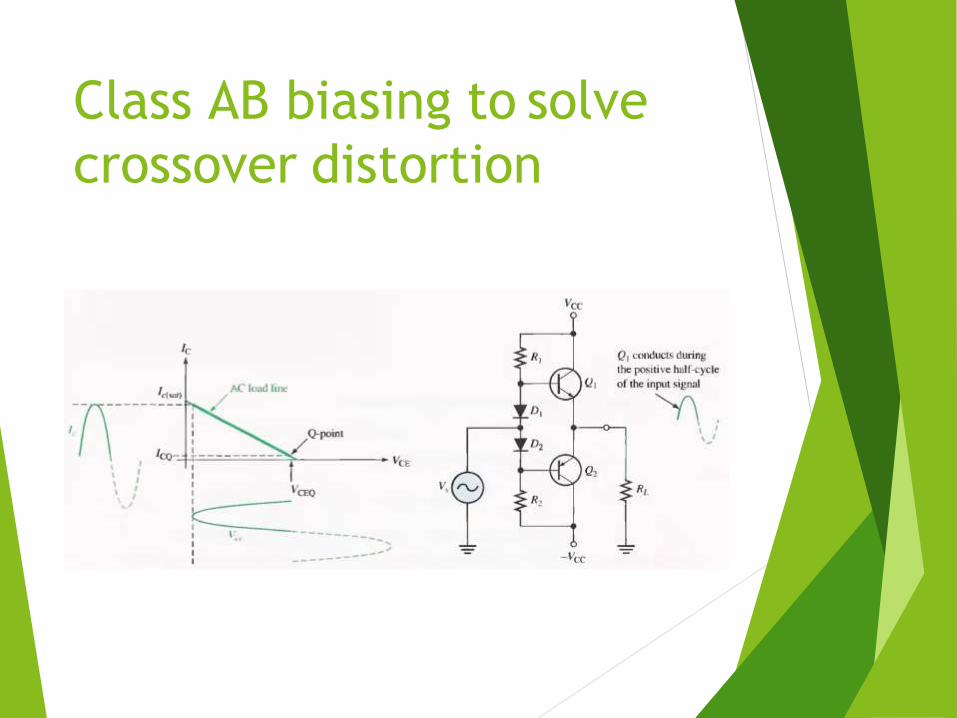
Class AB biasing to solve
crossover distortion
Complementary symmetry circuits
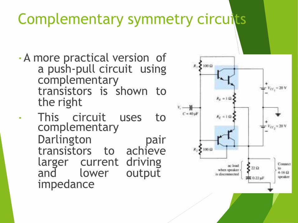
A more practical version ofa push-pull circuit usingcomplementarytransistors is shown tothe right
This circuit uses tocomplementaryDarlingtontransistors tolarger currentand lower
pairachievedrivingoutput
impedance
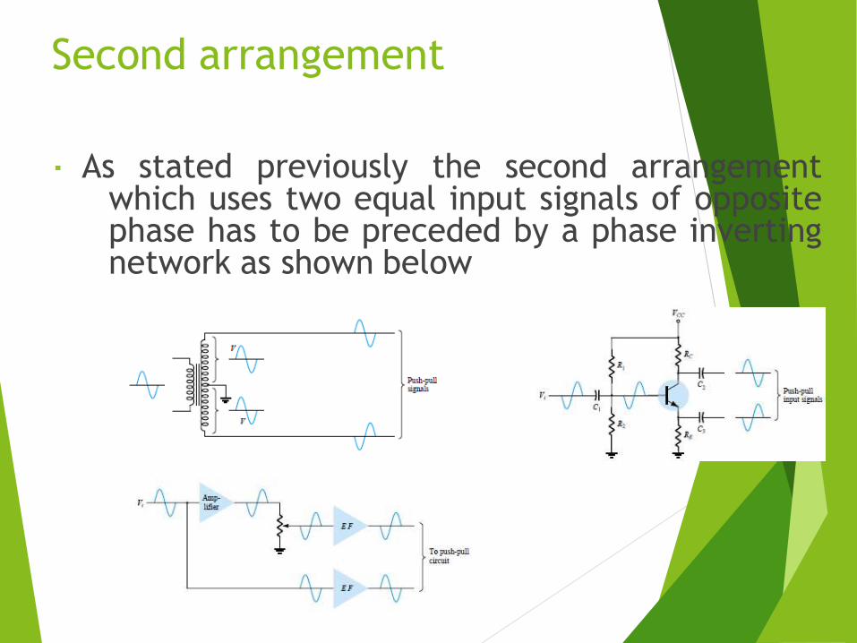
Second arrangement
As stated previously the second arrangementwhich uses two equal input signals of oppositephase has to be preceded by a phase invertingnetwork as shown below
Quasi-complementary push pull
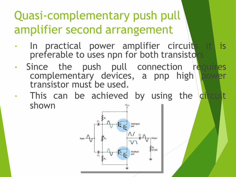
amplifier second arrangement
In practical power amplifier circuits it ispreferable to uses npn for both transistors
Since the push pull connection requirescomplementary devices, a pnp high powertransistor must be used.
This can be achieved by using the circuitshown
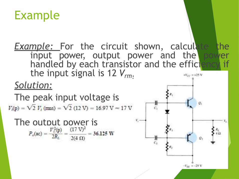
Example
s
Example: For the circuit shown, calculate theinput power, output power and the powerhandled by each transistor and the efficiency ifthe input signal is 12 Vrm
Solution:
The peak input voltage is
The output power is
Example
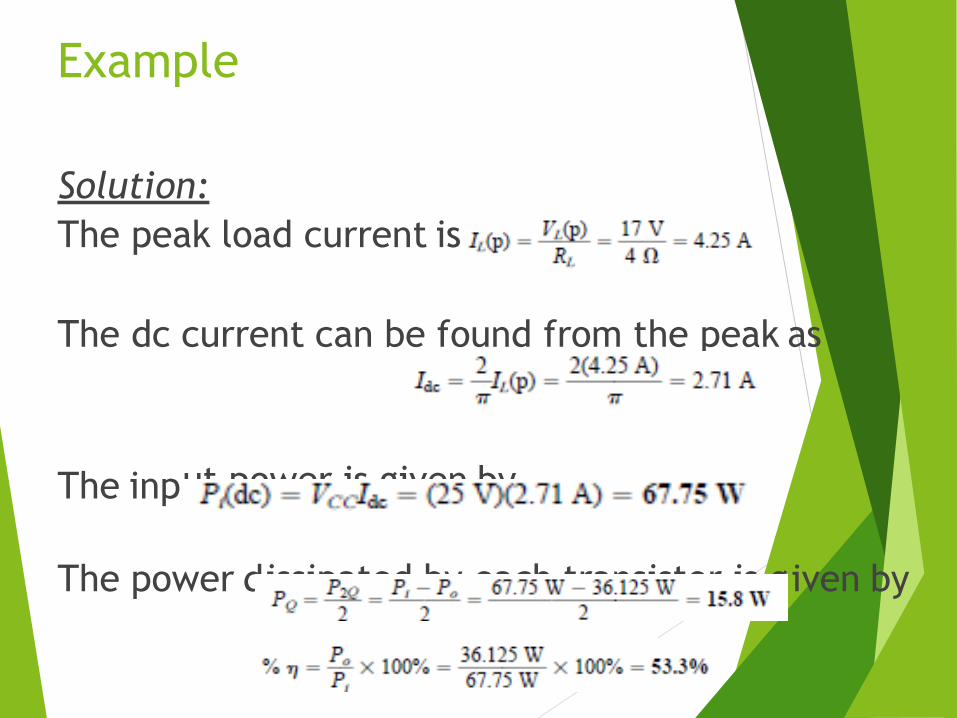
Solution:
The peak load current is
The dc current can be found from the peak as
The input power is given by
The power dissipated by each transistor is given by
Crossover Distortion
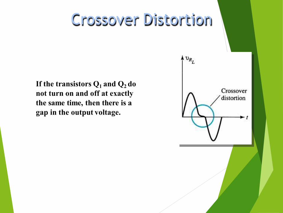
If the transistors Q1 and Q2 do not turn on and off at exactly the same time, then there is a gap in the output voltage.
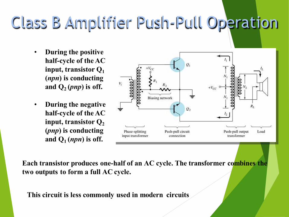
Class B Amplifier Push-Pull Operation
• During the positive half-cycle of the AC input, transistor Q1 (npn) is conducting and Q2 (pnp) is off.
• During the negative half-cycle of the AC input, transistor Q2 (pnp) is conducting and Q1 (npn) is off.
Each transistor produces one-half of an AC cycle. The transformer combines the two outputs to form a full AC cycle.
This circuit is less commonly used in modern circuits
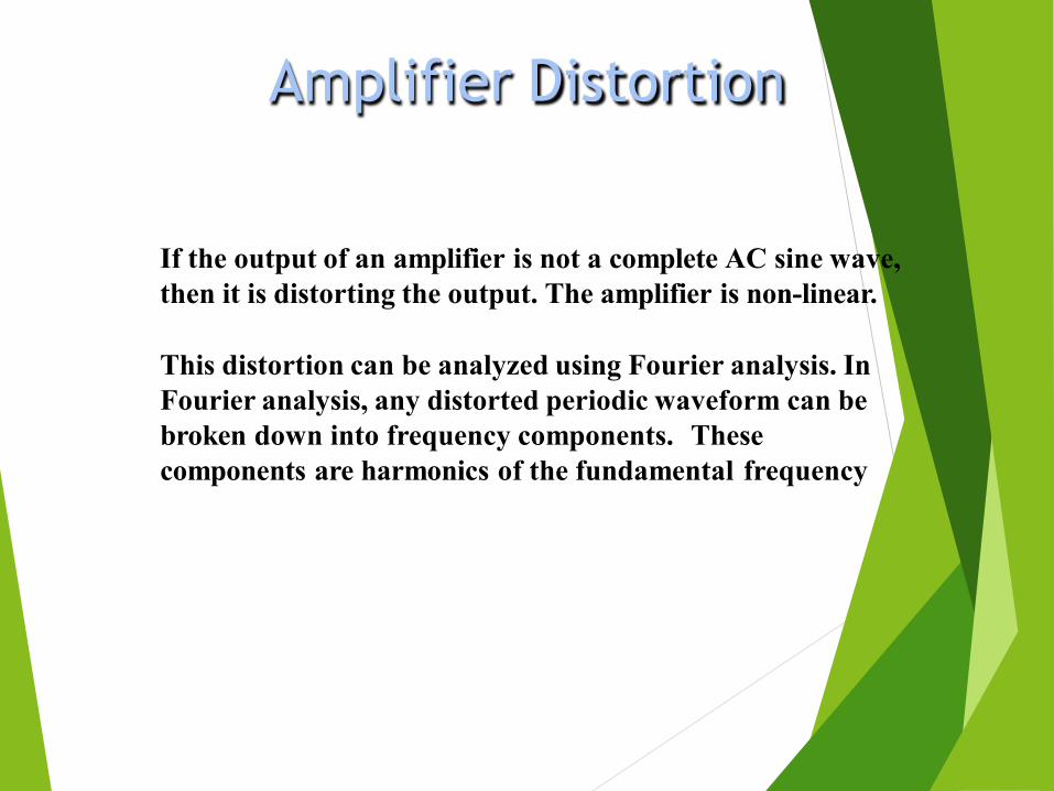
Amplifier Distortion
If the output of an amplifier is not a complete AC sine wave, then it is distorting the output. The amplifier is non-linear.
This distortion can be analyzed using Fourier analysis. In Fourier analysis, any distorted periodic waveform can be broken down into frequency components. These components are harmonics of the fundamental frequency
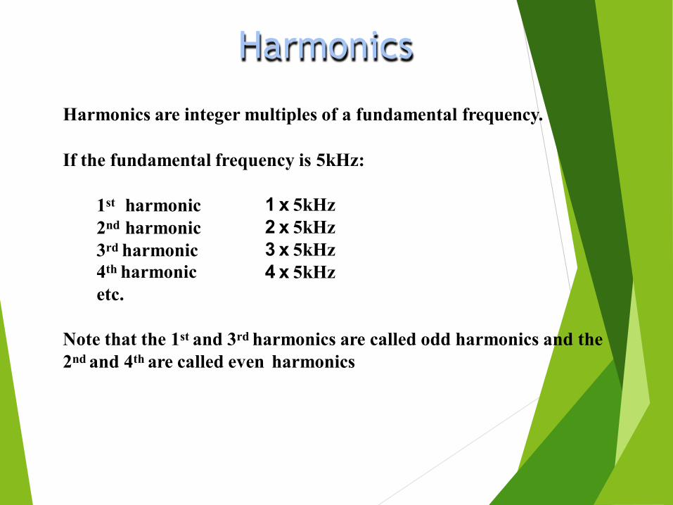
Harmonics
Harmonics are integer multiples of a fundamental frequency.
If the fundamental frequency is 5kHz:
1 x 5kHz2 x 5kHz3 x 5kHz4 x 5kHz
1st harmonic2nd harmonic3rd harmonic4th harmonicetc.
Note that the 1st and 3rd harmonics are called odd harmonics and the 2nd and 4th are called even harmonics

Harmonic Distortion
According to Fourier analysis, if a signal is not purely sinusoidal, then it contains harmonics.
241
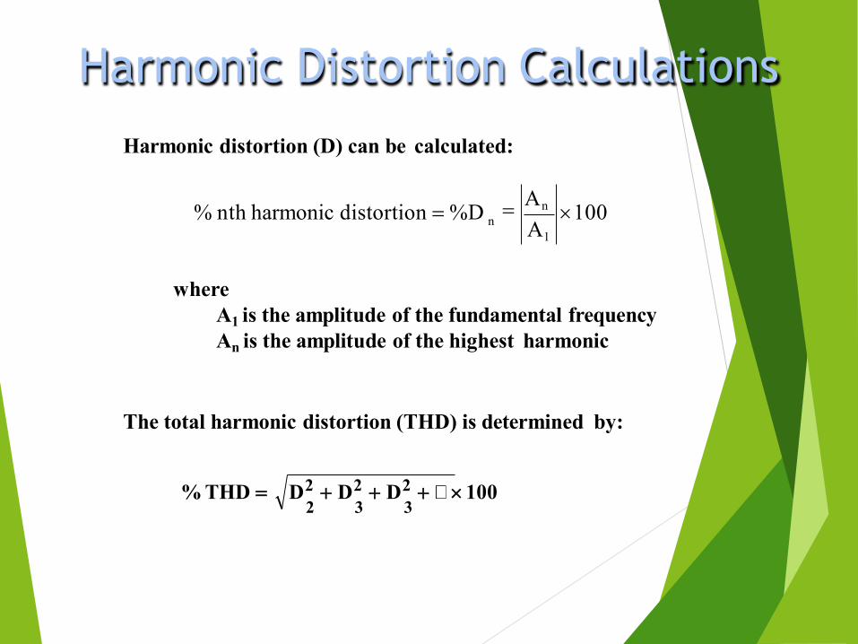
Harmonic Distortion Calculations
A1n 100
An% nth harmonic distortion %D
Harmonic distortion (D) can be calculated:
whereA1 is the amplitude of the fundamental frequency An is the amplitude of the highest harmonic
The total harmonic distortion (THD) is determined by:
% THD D2 D2 D2 1002 3 3
Power Transistor Derating Curve
Power transistors dissipate a lot of power in heat. This can be destructive to the amplifier as well as to surrounding components
Unit -4(b) LINEAR WAVE SHAPING
Wave Shaping
Definition: It is the process of changing the shape of input signal with
linear / non-linear circuits.
Types:
i. Linear Wave Shaping
ii. Non-linear Wave Shaping
Linear Wave Shaping
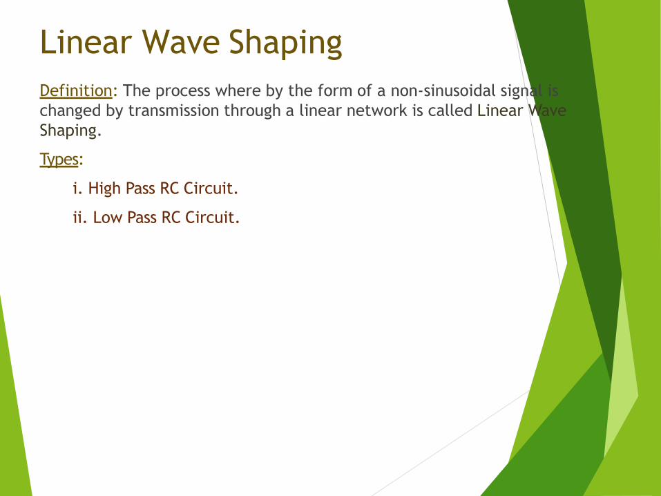
Definition: The process where by the form of a non-sinusoidal signal is
changed by transmission through a linear network is called Linear Wave
Shaping.
Types:
i. High Pass RC Circuit.
ii. Low Pass RC Circuit.
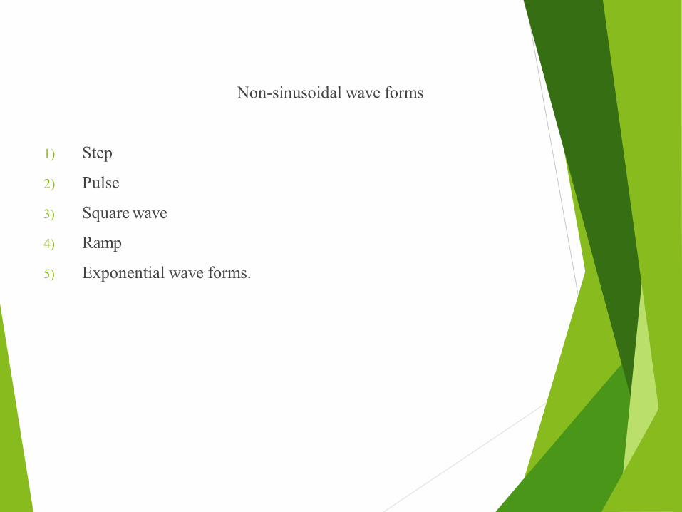
Non-sinusoidal wave forms
1) Step
2) Pulse
3) Square wave
4) Ramp
5) Exponential wave forms.

Step Waveform
tt=0
i
Vi=V
V =0 t<0
t>0
A step voltage is one which maintains the value zero for all times t<0 andmaintains the value V for all times t>0.
Vi
V
PulseThe pulse amplitude is ‘V’ and the pulse duration is tp.
0≤t≤tp
Otherwise
Vi=V
Vi=0
t=tpt
Vi
V
t=00
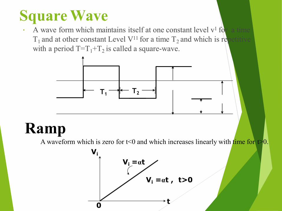
Square WaveA wave form which maintains itself at one constant level v1 for a time T1 and at other constant Level V11 for a time T2 and which is repetitive with a period T=T1+T2 is called a square-wave.
T1T2
RampA waveform which is zero for t<0 and which increases linearly with time for t>0.
Vi
Vi =αt
Vi =αt , t>0
0t

Exponentialwhere T is the time constant ofThe exponential waveform input is given by
the exponential input
Vi
0t
V

High pass RC circuit
R
+
VoC
+
-
Vi
-
If f=low, Xc becomes highC act as open circuit, so the Vo=0.
If f=high, Xc becomes lowC acts as short circuit, so we get the output.
The higher frequency components in the input signalappear at the output with less attenuation due to this behaviorthe circuit is called “High Pass Filter”.
XC 2fC
1
Sinusoidal input
For Sinusoidal input, the output increases in amplitude with increasing
frequency.
+
V
O
Vini
+
_ _
C
R
C
Vin Vini = =R - j X R - j
2πf C
Vini=R 1- j 2πf RC
OVin ×R VinV = i R = =
1- j2πf RC
j R 1 -2πf R C
Vo = iR
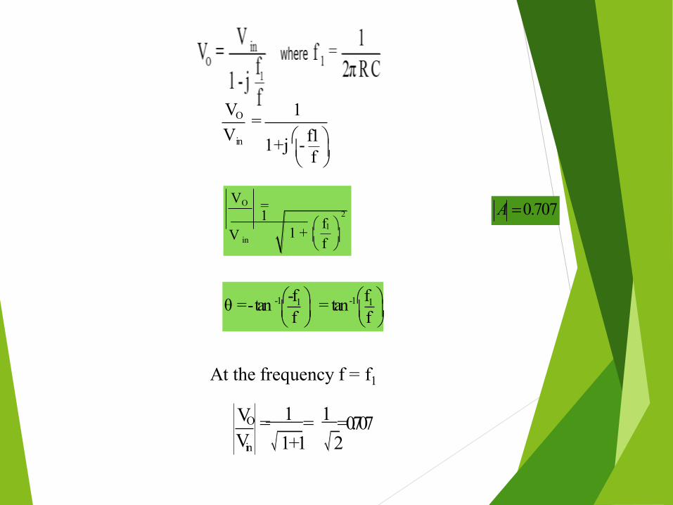
VO 1=V in 1 + j -f1
f
VO =1
V in
2 f 1 +
1
f
θ = -tan -1 -f1 = tan -1 f1 f f
At the frequency f = f1
VO
Vin
= 1 = 1 = 0.7071 + 1 2
A 0.707
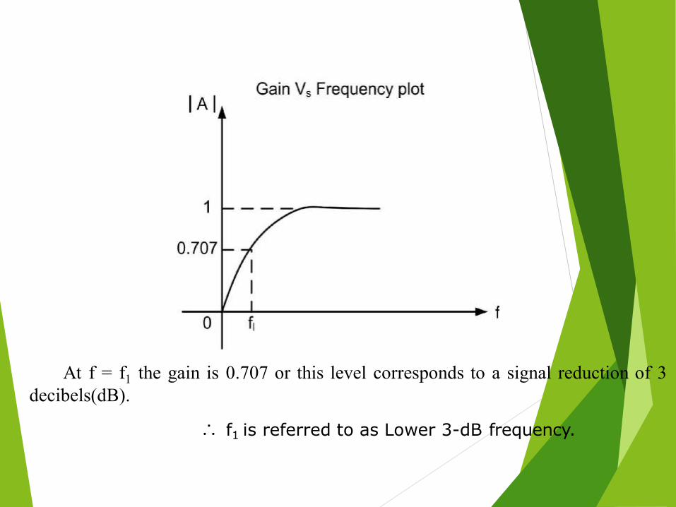
At f = f1 the gain is 0.707 or this level corresponds to a signal reduction of 3decibels(dB).
f1 is referred to as Lower 3-dB frequency.
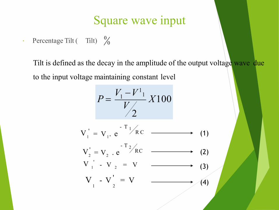
Square wave inputPercentage Tilt ( Tilt) 0
0
Tilt is defined as the decay in the amplitude of the output voltage wave due
to the input voltage maintaining constant level
2
11 X100VV V 1
P
1 1
- T 1R CV ' = V . e
2 2
- T 2RCV ' = V . e
1 2- V = VV '
V - V ' = V1 2
(1)
(2)
(3)
(4)

A symmetrical square wave is one for which T1=T2 = & because ofsymmetry V1 = - V2
By substituting these in above equation (3)
V=V1.e-T 2RC -V2
V=V1.e-T 2RC +V1
V=V1(1+e-T 2RC
)
I
Equation (1)
II

For RC>> T 2 the equation (I) & (II) becomes as
V TV1 (1+
2 4RC1
1)&V (1-V T2 4RC
)
11 1V -V
The percentage tilt ‘P’ is defined by P = V2
100

High Pass RC circuit acts as differentiator:-The time constant of high pass RC circuit in very small in comparisonwithin the time required for the input signal to make an appreciablechange, the circuit is called a “differentiator”.
Under this circumstances the voltage drop across R will be very small in comparison with the drop across C. Hence we may consider that the total input Vi appears across C, so that the current is determined entirely by the capacitance.
and the output signal across R isThen the current is i = C
V0 = iR
V0 = RC
hence the output is proportional to the derivative of the input.

Low Pass RC Circuit
If f=low, Xc becomes highC act as open circuit, so we get the output.
If f=high, Xc becomes lowC acts as short circuit, so Vo=0.
As the lower frequency signals appear at the output, it is called as“Low pass RC circuit”.
XC 1
2fC

Sinusoidal input
inV ×XC
jVO = XR + C
j
CX = 12fC
inV × 1
VO = 1R +
j C
j C
where
OVin VinV= =
jRC+ 1 1 + j 2fRC
iCS1Vo

OVinV =
1 + j ff2
21
where f =2RC
inA = VO = 1
V 1 + j ff2
A = 1
2 f 1 +
-1 fθ = - tan
f2
and
f2
At the frequency f = f2
VO
Vin
= 1 = 1 = 0.7071 + 1 2
A 0.707
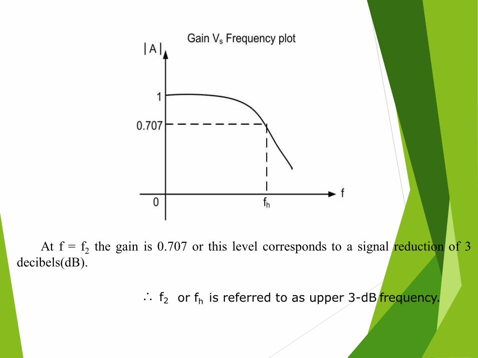
At f = f2 the gain is 0.707 or this level corresponds to a signal reduction of 3decibels(dB).
or fh is referred to as upper 3-dB frequency. f2
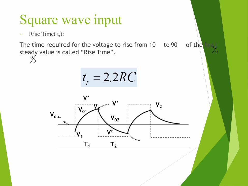
Square wave input
to 90 of the fina0l0
0
Rise Time( tr):
The time required for the voltage to rise from 10
steady value is called “Rise Time”.0
Vd.c.
V’
V01
V’ V2V2
V1
T1
V02
V’
T2

The output voltage V01 & V02 is given by
- T 1 RC= V 1 + (V1-V 1 ) . e ………………… (1)V01
V02
T= V 11 + (V2-V 11 ) . e - 2 RC ………………… (2)
if weset
andV01 = V2 at t=T1
V02= V1 at t= T1+T2
- T 1 RC1 1V2=V +( V1-V ) e
11 11 - T2
V1=V +( V2-V ) e RC
Since the average across R is zero then the d.c voltage at the output is same as that
of the input. This average value is indicated as Vd.c.
Consider a symmetrical square wave with zero average value, so that

T- 2RC2 1 + e
V 1 - e - T 2RCV =
T
TV e 2RC - 1
V2 = 2 e 2RC + 1V e2x - 1 TV2 = 2 . e2x + 1 where x = 4RC
2V = V tanhx2

Low pass RC circuit acts as an integratorThe time constant is very large in comparison with the time required for the input signal to make an appreciable change, the circuit is called an “Integrator”.
As RC>>T the voltage drop across C will be very small in comparison to the voltage drop across R and we may consider that the total input Vi appear and across R, then
Vi =iR
For low pass RC circuit the output voltage Vo is given by
OV = 1 i dtC
OV = 1 Vi dtC R
O iV = 1 V dtRC
Advantages of Integrator over differentiatorIntegrators are almost invariably preferred over differentiators inanalog computer applications for the following reasons.
The gain of the integrator decreases with frequency where as the gain of the differentiator increases linearly with frequency. It is easier to stabilize the former than the latter with respect to spurious oscillations.
As a result of its limited band width an integrator is less sensitive to noise voltages than a differentiator.
If the input wave form changes very rapidly, the amplifier of a differentiator may over load.
It is more convenient to introduce initial conditions in an integrator.

UNIT-V:
Switching Characteristics of Devices
269

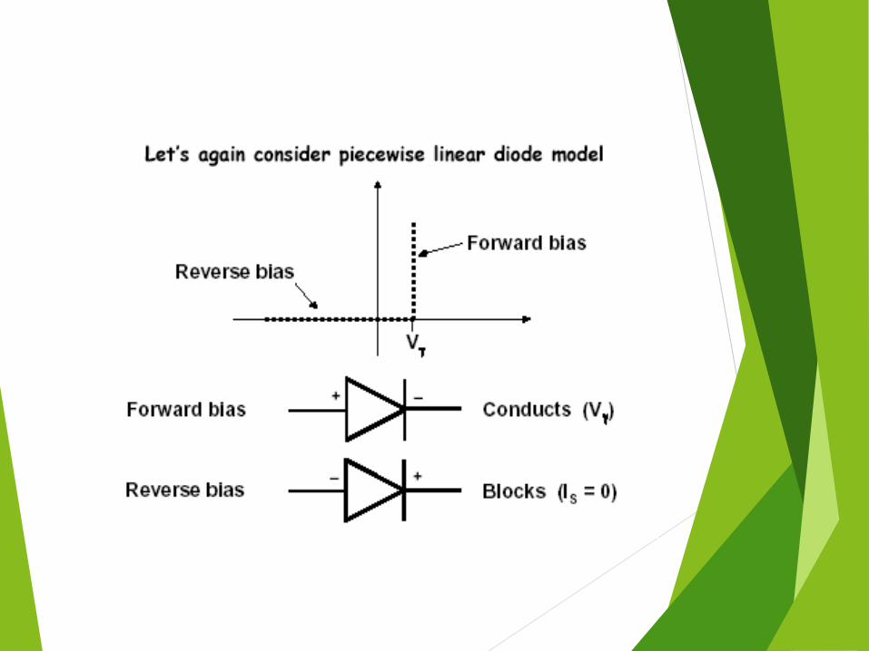
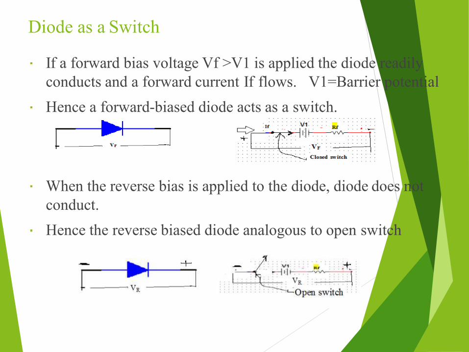
SWITCHING CHARACTERISTICS OF DEVICES DIODEAS A SWITCH The diode readily conducts when forward-biased and the bias
voltage is greater than the cut-in voltage. There is no conduction through the device ,when it is reverse
biased. The forward resistance of an ideal diode is zero, and the reverse
resistance is infinitely large. A diode conducts when forward-biased and blocks conduction
when reverse-biased, it can function as an electronic switch. When it is conducting , it is ON, and when it is not conducting it is
OFF.
Diode as a Switch
If a forward bias voltage Vf >V1 is applied the diode readilyconducts and a forward current If flows. V1=Barrier potentialHence a forward-biased diode acts as a switch.
When the reverse bias is applied to the diode, diode does not conduct.Hence the reverse biased diode analogous to open switch
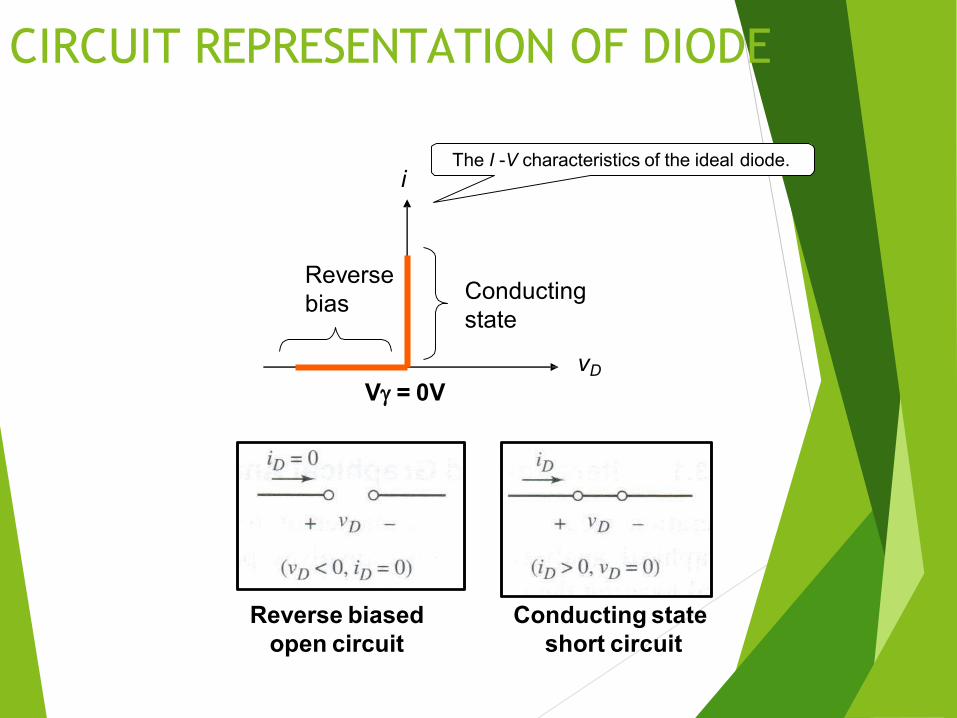
CIRCUIT REPRESENTATION OF DIODE
iThe I -V characteristics of the ideal diode.
V = 0V
Conductingstate
vD
Reverse bias
Reverse biasedopen circuit
Conducting stateshort circuit
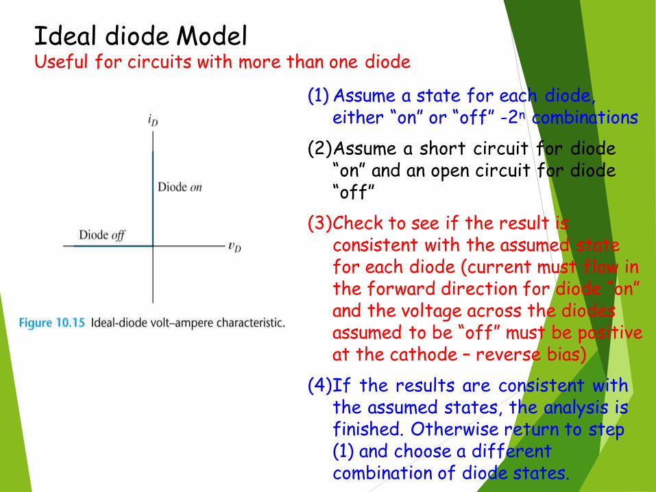
Ideal diode ModelUseful for circuits with more than one diode
(1) Assume a state for each diode,either “on” or “off” -2n combinations
(2)Assume a short circuit for diode“on” and an open circuit for diode“off”
(3)Check to see if the result is consistent with the assumed state for each diode (current must flow in the forward direction for diode “on” and the voltage across the diodes assumed to be “off” must be positive at the cathode – reverse bias)
(4)If the results are consistent withthe assumed states, the analysis isfinished. Otherwise return to step(1) and choose a differentcombination of diode states.

CIRCUIT REPRESENTATION OF DIODE
– Piecewise Linear Model
i
V
Conductingstate
vD
Reverse bias
VD = V for diode to turn on.
Hence during conducting state:
=V
Represented as a battery of voltage = V
Reverse biasedopen circuit

i
V
Conductingstate
vD
Reversebias
CIRCUIT REPRESENTATION OFDIODE – Piecewise Linear Model
VD ≥ V for diode to turn on.
Hence during conductingstate:
Reverse biasedopen circuit
=V
Represented as a battery of voltage = V and forward resistance, rf in seriesrf
+ VD -

Transistor as a switchA transistor can be used as a switch.It has three regions of operationWhen both EB junction and CB junction are reverse biased, the transistor operates in the cut-off region.When the EB junction is forward biased and CB junction is reverse biased , it operates in the active region and acts as an amplifier.When both the EB junction and CB junctions are forward biased it operates in the saturation region and acts as a closed switch.When Q is saturated it is like a closed switch from C to E.
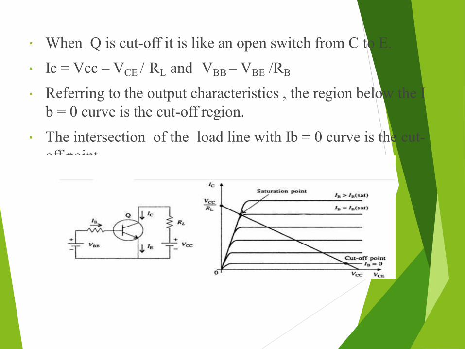
When Q is cut-off it is like an open switch from C to E.Ic = Vcc – VCE / RL and VBB – VBE /RB
Referring to the output characteristics , the region below the Ib = 0 curve is the cut-off region.The intersection of the load line with Ib = 0 curve is the cut-off point.

Ib =The intersection of the load line withtheIb(sat) curve is called the saturationpoint.At this point the base current is Ib(sat) and thecollector current is maximum.Ic(sat) = Vcc/RL
Ib(sat) represents the minimum base current requiredto bring the transistor intosaturation.For 0<Ib<Ib(sat), the transistor operates in the activeregion.If the base current is greater than Ib(sat),Ic ≈≈Vcc/Rc and transistor appears like a closed switch.
Breakdown voltage of a Transistor
The maximum reverse biasing voltage which may be applied before breakdown between the collector and base terminal of the transistor(BVCBO)i.e the emitter lead be open circuited.The breakdown occurs because of the avalanchemultiplication of the current Ico that crosses the collector junction.As the multiplication the current becomes Mico.
M = 1/1-(VCB /BVCBO)n M = Multiplication factorThe parameter n lies in the range 2 to 10.Below Fig. shows the CB characteristics in the breakdownregion.The curve for Ie =0 is function of Vcb.Ic has magnitude MάIE.

Breakdown voltage of a transistor

The transistor switch in saturation
In the fast switching circuits, RL must be kept small.In saturation the transistor current is normally Vcc/ RL.
The total voltage swing at the transistor switch is Vcc-Vce(sat).
At Ib = -0.15mA the transistor is in saturation and Vce=-175mvAt Ib = -0.35mA Vce has dropped to 100mvFor a transistor operating in the saturation region a quantity of interest is the ratio Vce(sat)/Ic. This parameter is called the common emitter saturation resistance, Rce(sat).The saturation voltage Vce(sat) depends not only on the operating point but also on the semiconductor material.In the saturation region hfe is a useful parameter and is suppliedby the manufacturer.Once we know Ic(Vcc/RL) and hfe, the amount of base currentIb = Ic/hfe needed to saturate the transistor can be found.

Design of Transistor switchThe transistor that acts as a switch is driven between cut-off and saturation.
For low input vi =0 the transistor is kept at cut-off, so the output is Vcc or1.
For high input , the transistor is driven into saturation. So the output i.eVce(sat) = 0. Thus the transistor acts as a switch.
To improve the transient response of the inverter the capacitor C is usedacross the resistor R1.
This helps in removing minority carrier charges in the base when the signal changes between logic states.

Design: when vi=0 the open circuit base voltage isVb=-Vbb (R1/R1+R2). This voltage should be less than Vbe(cut-off).When vi=1, the transistor is in saturation.Ic=(Vcc-Vce(sat))/Rc and Ib(min) = Ic/hfe(min)The current through the resistance R1 is I1=(V(1)-Vbe(sat))/R1The current throhgh the resistor R2 is I2=[Vbe(sat)-(-Vbb)]/R2Ib = I1-I2This current Ib must be equal to Ic/hfe =Vcc-Vce(sat)/Rc.hfeRc = [Vcc-Vce(sat)]/IcAssuming the values of Vbe(sat) and Vce(sat).Select R1 and R2 such that I1-I2 = Ib

Diode switching Times
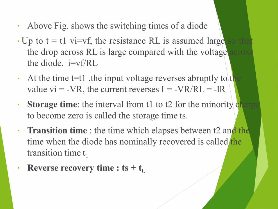
Above Fig. shows the switching times of a diodeUp to t = t1 vi=vf, the resistance RL is assumed large so that
the drop across RL is large compared with the voltage acrossthe diode. i=vf/RLAt the time t=t1 ,the input voltage reverses abruptly to the value vi = -VR, the current reverses I = -VR/RL = -IRStorage time: the interval from t1 to t2 for the minority chargeto become zero is called the storage time ts.Transition time : the time which elapses between t2 and the time when the diode has nominally recovered is called the transition time tt.
Reverse recovery time : ts + tt.

Transistor switching Times
When the transistor acts as a switch , it is either in cut-off or in saturation.To consider the behavior of the transistor as it makes transitionfrom one state to the other.

The pulse waveform makes the transitions between the voltage levels V2 and V1. At V2 the transistor is at cut-off and at V1 the transistor is in saturation.The input waveform vi is applied between the base and the emitter through a resistor RB .
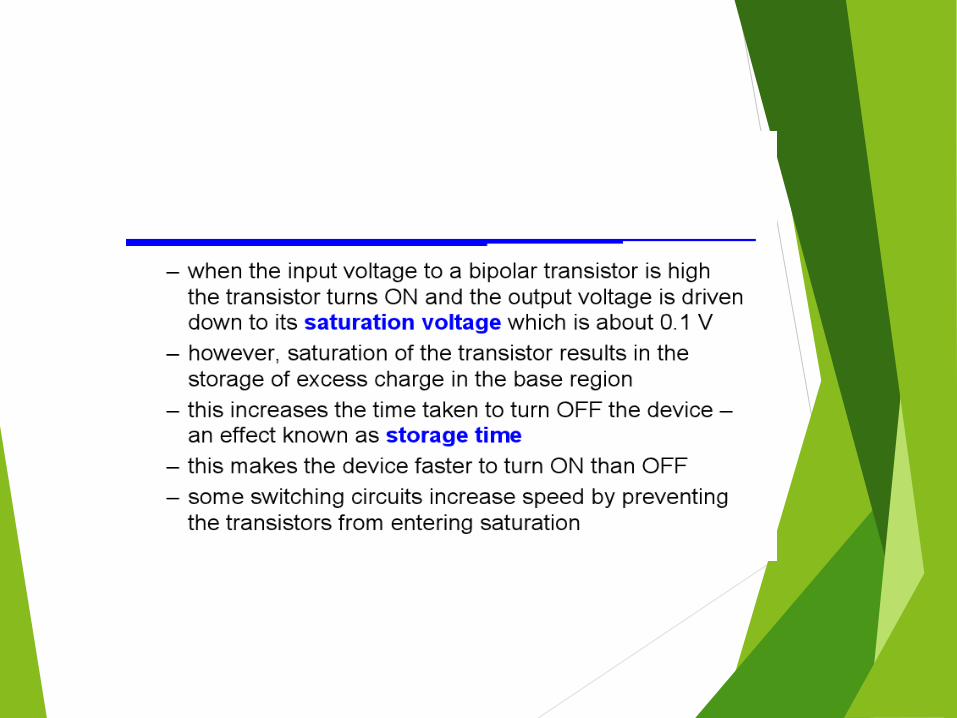
The collector current does not immediately respond to theinput signal.Delay time(td) : The interval of time between the application of the base current and the commencement of collector current is termed as delay time(td)Rise time(tr) : The time required for the collector current to rise from 10% to 90% of the maximum level.Turn-on time tON = td +tr

Storage time(ts) : There is a time lag between the instantIb =0 and the instant at which Ic begins to decrease. Thisinterval is termed as storage time.Fall time(tf) : The time required to fall from 90% to 10% ofmaximum value is termed as fall tome.Turn-off time tOFF = ts +tf
Decay time : The collector current falls from 10% to level ofIcbo. It is very small.


