
B.Supmonchai September 22nd, 2004
2102-545 Digital ICs 1
Chapter 10
Testing and Design for Testability
Boonchuay SupmonchaiIntegrated Design Application Research (IDAR) Laboratory
September 22nd, 2004
2102-545 Digital ICs IC Testing 2
B.Supmonchai
Goals of This Chapterq To provide a background on general testing
ß Fault Modeling
ß Test Generation
ß Faults Simulation
ß IDDQ Testing
q To present general techniques on Design for Testability
ß Scan-Based
ß Boundary Scan
ß Build-In Self Test (BIST) Techniques
2102-545 Digital ICs IC Testing 3
B.Supmonchai
The Testing Problemq The goal of testing is to detect manufacturing defects in
digital ICs/Components as earlier as possible withminimum costsß Times to design and test
ß Silicon area to be used
q Costs increase dramatically as faulty components findtheir way into higher levels of integration.ß $1 to fix an IC (so throw it out!)
ß $10 to find and replace bad IC on a PC board
ß $100 to find bad PC board in a system
ß $1000 to find bad component in fielded system
2102-545 Digital ICs IC Testing 4
B.Supmonchai
Test Classification
q Diagnostic test
ß Used in chip/board debugging
ß Defect localization
q “go/no go” or production test
ß Used in chip production
q Parametric test
ß x Œ [v,i] versus x Œ [0,1]
ß Check parameters such as NM, Vt, tp, T

B.Supmonchai September 22nd, 2004
2102-545 Digital ICs 2
2102-545 Digital ICs IC Testing 5
B.Supmonchai
Testing Procedureq Apply a set of test vectors to each device off the
manufacturing line and compare outputs to the knowngood response
q The optimum test set will detect the greatest number ofdefects that can be present in a device with the leastnumber of vectors.
q Development of the optimal test set is the most difficultpart of the process.ß A longer test set takes more time to apply to each device ($$$).
q There are a number of different approaches to test setgeneration.
2102-545 Digital ICs IC Testing 6
B.Supmonchai
Types of Testq Exhaustive Testß Applies every possible input vector
ß Guaranteed to detect all detectable faults
ß Impractical in terms of number of tests required
q Functional Testß Tests every function of the device
ß Also detects every detectable faults if completed
ß Provides a smaller test set size than exhaustive testsbut requires more time for the designers to findoptimum test vector
2102-545 Digital ICs IC Testing 7
B.Supmonchai
Type of Test (cont.)q Fault Model Derived Testß Finds a test for every “modeled” fault
ß To develop tests of all detectable modeled faults isusually a tractable problem.
ß The most practical method for test vector generationis to develop a model of the physical defects that canoccur in the fabricated device at a higher level ofabstraction (typically the logic level), and thendevelop tests for these modeled faults.
ß Depending on the quality of the fault model, a testvector will most often cover a high percentage of theactual physical defects.
2102-545 Digital ICs IC Testing 8
B.Supmonchai
Example: Which Type of Test?
q Consider a 74181 ALU chip - 14 inputs
Fault modeldetermines thequality (coverage)
There is no algorithmicway to verify that allfunctional modes havebeen covered
At 10 MHz, a 16-bitALU with 38 inputswould take 7.64 hours
Notes
47448 ~ 8 for each logic mode ~ 20 for each arithmetic mode
16384Number oftest vectors
100 %
(modeled faults)
100 %100 %Faultcoverage
Modeled faultFunctionalExhaustiveType of test

B.Supmonchai September 22nd, 2004
2102-545 Digital ICs 3
2102-545 Digital ICs IC Testing 9
B.Supmonchai
Current Testing Practiceq For most ASIC designs, the typical practice is to begin
with the designer’s functional test set.
q This set of vectors is fault simulated to determine its faultcoverage.ß If the coverage is too low to be acceptable, more functional
vectors can be added to exercise the portions of the circuitwhere the undetected faults lie.
ß A more efficient approach is to feed the list into an AutomaticTest Pattern Generation (ATPG) program to develop the test.
q Another approach used is to apply Design for Test (DFT)or Build-In Self-Test (BIST) Techniques as part of thedesign process.ß IBM’s Level Sensitive Scan Design
2102-545 Digital ICs IC Testing 10
B.Supmonchai
Fault Attributes
Fault Characteristics
Cause Duration Value
SpecificationMistakes
ImplementationMistakes
External Disturbances
ComponentDefects
Nature
Hardware Software
Analog Digital
Permanent Transient
Intermittent
Determinate
Indeterminate
Extent
Local Global
2102-545 Digital ICs IC Testing 11
B.Supmonchai
Fault Modelingq The trade-off in fault modeling is to develop a model
that is as simple as possible to use in test generationwhile detecting as high as possible the percentage ofphysical defects.
q Most common fault models
ß Stuck-at faults
ÿ Single stuck-at (s-a) faults
ÿ Multiple stuck-at (m-a) faults
ß Stuck-open faults
ß Bridging faults
ß Delay faults
2102-545 Digital ICs IC Testing 12
B.Supmonchai
Single Stuck-at Fault Modelq Assumptionsß Only one line in the circuit is faulty at a time
ß The fault is permanent (as opposed to transient)
ß The effect of fault is as if the faulty node is tied to either VCC(s-a-1), or GND (s-a-0) (short circuits!)
ß The function of the gates in the circuit is unaffected by the fault
VCC
A
BC
111
001
010
000
CBA
111
001
110
000
CBA
Fault-Free Gate Faulty GateFault: s-a-1
Most often used because of its simplicity during test generation and fault simulation

B.Supmonchai September 22nd, 2004
2102-545 Digital ICs 4
2102-545 Digital ICs IC Testing 13
B.Supmonchai
Single Stuck-at Fault Model IIq Advantageß Can be applied at the logic level or module level
ß Reasonable number of faults 2n (n = # of circuit nodes)
ß Algorithms for ATPG and fault simulation are well developedand efficient.
ß Single stuck-at fault model can cover about 90% of thepossible manufacturing defects in CMOSÿ Source-drain shorts, oxide pinholes, missing features, diffusion
contaminants, metallization shorts, etc.
ß Other useful fault models (stuck-open, bridging faults) can bemapped into (sequences of) stuck-at faults
q Disadvantageß Does not cover all defects in CMOS or other devices
2102-545 Digital ICs IC Testing 14
B.Supmonchai
Stuck-Open Fault Modelq Assumptionsß A single physical line in the circuit is broken
ß The resulting unconnected node is not tied to either VCC or GND.
VDD
A
BF
LineBreak
q Line Break results in a“memory effect” in thebehavior of the circuit
q With AB = 10, there is nopath from either VDD or GNDto the output
ß F retains the previous valuefor some undetermineddischarge time.
2102-545 Digital ICs IC Testing 15
B.Supmonchai
Stuck-Open Fault Modelq Advantagesß Covers physical defects not covered by single or multiple stuck-
at fault models
ß Can be tested with sequences of stuck-at fault testsÿ In the NOR gate example, apply AB = 00 (test for F s-a-0) forcing
F to VCCÿ Then apply AB = 10 (test for A s-a-0) to force F to GND and
observe results.
q Disadvantagesß Requires a larger number of tests (sequence for each fault)
ß Algorithms for ATPG and fault simulation are more complexand less well developed
ß Requires a lower level circuit description, at least fordevelopment of the fault list
2102-545 Digital ICs IC Testing 16
B.Supmonchai
Test Generation Process
CUT
A s-a-0A s-a-1B s-a-0B s-a-1C s-a-0C s-a-1D s-a-0D s-a-1E s-a-0E s-a-1F s-a-0F s-a-1...
A s-a-0
÷A s-a-0A s-a-1B s-a-0B s-a-1C s-a-0C s-a-1D s-a-0D s-a-1E s-a-0E s-a-1F s-a-0
÷F s-a-1...
A s-a-0F s-a-1H s-a-1M s-a-0N s-a-1...
A B C D E
1 0 1 X X
Generate list of undetected Fault (Collapse)
Select a fault for test
generation
Generate a test vector for that fault (ATPG)
Generate a list of other Faults detected by that
Test vector(Fault Simulation)
Mark those Detected faults off
the fault list
LOOP: select anUndetected fault
For test generation
EXIT when all faultsAre detected or Proven unstable

B.Supmonchai September 22nd, 2004
2102-545 Digital ICs 5
2102-545 Digital ICs IC Testing 17
B.Supmonchai
Automatic Test Pattern Generationq The objective is to automatically generate a test for
faults in the circuit-under-testß Deterministic (or heuristic) - require expertise
ß Random - or more appropriately Pseudorandom
q Major classes of methodsß Pseudorandom
ß Ad-Hoc
ß Algorithmicÿ D-algorithm
ÿ PODEM
ÿ FAN and related algorithms
ÿ Others …
2102-545 Digital ICs IC Testing 18
B.Supmonchai
Pseudorandom Test Generationq Simply generate an input vector using a pseudorandom
number generator and perform fault simulation todetermine if it detects the target fault.
q The characteristics of the fault greatly influence howwell pseudorandom test generation will work
ß Easy-to-detect faults
ß Hard-to-detect faults
q Typically used in the beginning of the test generationprocess to remove easy-to-detect faults from the faultlist.
2102-545 Digital ICs IC Testing 19
B.Supmonchai
Pseudorandom Test Generation II
Typically pseudorandom tests are generated and fault simulated until twoor more successive pseudorandom vectors fail to detect any new faults.Then deterministic ATPG processes are used to target the remainingundetected faults.
2102-545 Digital ICs IC Testing 20
B.Supmonchai
Ad-Hoc Test Generationq Uses functional test vectors developed by designers for
functional verification and design debugging byß Fault simulating to determine fault coverage
ß Determining locations of undetected faults
ß Adding additional functional tests to exercise areas of designwith undetected faults
ß Re-fault simulating and repeating until desired fault coverageis achieved
q No special test generation system is required, only faultsimulator - use existing vectors and designer expertise.
q Achieving high fault coverage may be difficult and timeconsuming - especially for synthesized designs

B.Supmonchai September 22nd, 2004
2102-545 Digital ICs 6
2102-545 Digital ICs IC Testing 21
B.Supmonchai
Fault Table
A
BC = A NOR B
0
1
1
1
1
1
1
1
1
1
1
1
0
0
0
0
0
1
0
1
0
0
1
1
T4 = 11
T3 = 10
T2 = 01
T1 = 00
1
1
1
1
f0 = n
o fau
lt
f1 = A
s-a-0
f2 = B
s-a-0
f3 = C
s-a-0
f4 = A
s-a-1
f5 = B
s-a-1
f6 = C
s-a-1
TestVector
1
f1
1
f2
1
1
1
f3
1
f4
1
f5
1
f6
T4
T3
T2
T1
f3 dominates f4 and f5
f1, f2 , and f6 are equivalent
Good/Faulty Circuit Responses Fault Table
To construct fault table of XORInsert a test vector, record theresponse of the circuit, and comparewith the known good result (f0)
2102-545 Digital ICs IC Testing 22
B.Supmonchai
Fault Table Reduction
1
f1
1
f2
1
1
1
f3
1
f4
1
f5
1
f6
T4
T3
T2
T1
1
f4
1
f5
1
f6
T4
T3
T2
T1
1
f4
1
f5
1
f6
T4
T3
T2
T1 1
f4
1
f5
1
f6
T4
T3
T2
To collapse faults,Remove all but one ofequivalent columns andall dominating columns
To collapse rows,Remove all but one ofequivalent rows and alldominated columns
Fault Table Collapsed Fault Table
Collapsed Fault Table Reduced Fault Table
Note: an empty row (e.g., T1 is dominated by every row)
2102-545 Digital ICs IC Testing 23
B.Supmonchai
Fault Simulation Algorithmsq Goal: determine the list of faults in a CUT that are
detected by a specific test vector
q The general procedure is to simulate the good and faultycircuits and determine if they produce different outputs
q Consists of five specific tasks:
ß Good circuit simulation
ß Fault specification (fault list generation and collapsing)
ß Fault insertion
ß Fault-effect generation and propagation
ß Fault detection and discarding2102-545 Digital ICs IC Testing 24
B.Supmonchai
Fault Simulation Algorithms IIq Fault simulation is one of the most widely used of the
test technologies presented herein - many efficientalgorithms for fault simulation have been developed.
q Major types:
ß Parallel fault simulation
ß Deductive fault simulation
ß Concurrent fault simulation
ß Parallel Pattern Single Fault Propagation (PPSFP)
q Most other work on fault simulation has been inimproving the efficiency of these types of faultsimulation or actually paralleling the fault simulationalgorithms to be run on parallel/distributed computers

B.Supmonchai September 22nd, 2004
2102-545 Digital ICs 7
2102-545 Digital ICs IC Testing 25
B.Supmonchai
IDDQ Testingq IDDQ testing is becoming more prevalent both in
research and in new industrial applications.ß All of the test techniques discussed thus far use voltage
measurement techniques.
q IDDQ testing is based on the physical fact that fault-freeCMOS circuits consume VERY LITTLE current in thequiescent state.ß Quiescent current for MOS devices (IDDQ) is typically in the
fA range
q The presence of faults, under the right conditions, canincrease this quiescent current by several orders ofmagnitude which can be used to detect the fault.
2102-545 Digital ICs IC Testing 26
B.Supmonchai
IDDQ Testing II
When input goes, PMOS turns on and significant current flows betweenthe source and gate such that IDDQ increases dramatically. However,because the gate output goes high as it should, traditional stuck-at faulttesting would not detect this defect.
2102-545 Digital ICs IC Testing 27
B.Supmonchai
Advantages of IDDQ Testingq Test generation is easierß Faults must be activated, but not propagated to a Primary
Output
q IDDQ testing can detect defects that are not modeled bythe stuck-at modelß Bridging faults
ß Gate oxide defects
ß Shorts between any two of the four terminals of a transistor
ß Partial defects - defects that do not affect the logic of thecircuit, but may effect reliability
ß Some delay faults
ß Some stuck-open faults
2102-545 Digital ICs IC Testing 28
B.Supmonchai
Disadvantages of IDDQ Testingq Since normal IDDQ is very low, measurements must be
very preciseß Measurement takes a significant amount of time (1 ms)
relative to the voltage measurement techniques
ß Setting IDDQ threshold for bad devices is hard
q Circuit-under-test must be suitable for IDDQ testing -certain restrictions must be placed on the designß Must contain all static devices (which is slower), i.e., noÿ Dynamic circuitry
ÿ Pull-ups or pull-downs on I/O buffers
ÿ Specialized speed optimized circuitry such as RAM sense ampsthat draw significant static current
B.Supmonchai September 22nd, 2004
2102-545 Digital ICs 8
2102-545 Digital ICs IC Testing 29
B.Supmonchai
IDDQ Fault Modelingq There are several fault models that can be used for IDDQ test
generation - all of them at the logic or transistor level.
ß Stuck-at Fault Model
ÿ Drive the faulty node to the value opposite the stuck-at value
ß Transistor Short Model
ÿ Specific patterns can be derived to test for all possible combinations ofshorts between all four terminals
ß Bridging Fault Model
ÿ Only physically adjacent nodes need to be tested
ÿ Drive the adjacent nodes to opposite values
2102-545 Digital ICs IC Testing 30
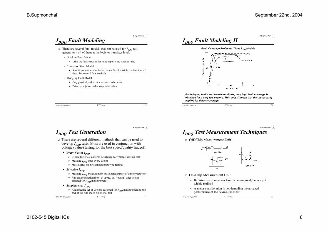
B.Supmonchai
IDDQ Fault Modeling IIFault Coverage Profile for Three IDDQ Models
For bridging faults and transistor shorts, very high fault coverage isobtained for a very few vectors. This doesn't mean that this necessarilyapplies for defect coverage.
2102-545 Digital ICs IC Testing 31
B.Supmonchai
IDDQ Test Generationq There are several different methods that can be used to
develop IDDQ tests. Most are used in conjunction withvoltage (value) testing for the best speed/quality tradeoff.ß Every Vector IDDQ
ÿ Utilize logic test patterns developed for voltage-sensing testÿ Measure IDDQ after every vectorÿ Most useful for first silicon prototype testing
ß Selective IDDQ
ÿ Measure IDDQ measurement on selected subset of entire vector setÿ Run entire functional test at speed, but “pause” after vector
selected for IDDQ measurement
ß Supplemental IDDQ
ÿ Add specific set of vectors designed for IDDQ measurement to theend of the full-speed functional test
2102-545 Digital ICs IC Testing 32
B.Supmonchai
IDDQ Test Measurement Techniquesq Off-Chip Measurement Unit
q On-Chip Measurement Unitß Built-in current monitors have been proposed, but not yet
widely realized
ß A major consideration is not degrading the at-speedperformance of the device-under-test

B.Supmonchai September 22nd, 2004
2102-545 Digital ICs 9
2102-545 Digital ICs IC Testing 33
B.Supmonchai
IDDQ Design for Testability
q In order to ensure/improve IDDQ testability,several design constraints must be applied tolimit good circuit IDDQ.
ß Internal Tri-state Busesÿ Short periods of bus contention may be functionally OK,
but cause problems with IDDQ testabilityÿ Design controllers for non-overlapping bus drivers
ß Pull-ups and Pull-downsÿ Pull-up (down) resistors are commonly used in I/O padsÿ Eliminate or use separate power supply for I/O pads
2102-545 Digital ICs IC Testing 34
B.Supmonchai
IDDQ Design for Testability II
q Design Constraints (continued)
ß Dynamic Circuitryÿ Precharge/discharge type logic typically used for high-
speed design
ÿ Ensure all nodes are precharged on every clock cycle
ß Circuits with Non-Zero Static Currentÿ Sense-Amps for memory cells, etc.
ÿ Avoid or use separate power supply
2102-545 Digital ICs IC Testing 35
B.Supmonchai
Design for Testability
M state regs
N inputs K outputs
K outputsN inputsCombinational
Logic
Module
Combinational
Logic
Module
(a) Combinational function (b) Sequential engine
2N patterns 2N+M patterns
Exhaustive test is impossible or unpractical
M state regs
N inputs K outputs
K outputsN inputsCombinational
Logic
Module
Combinational
Logic
Module
(a) Combinational function (b) Sequential engine
2N patterns 2N+M patterns
2102-545 Digital ICs IC Testing 36
B.Supmonchai
Design for Testability IIq Goal: increase the ease with which a device can be testedß Increase the controllability and observability of internal points
in the circuit
q Three major approachesß Ad-hoc DFT techniques
ß Scan-based DFT techniques
ß Self-Test (BIST) techniques
q Problem is getting harderß Increasing complexity and heterogeneous combination of
modules in system-on-a-chip.
ß Advanced packaging and assembly techniques extend problemto the board level

B.Supmonchai September 22nd, 2004
2102-545 Digital ICs 10
2102-545 Digital ICs IC Testing 37
B.Supmonchai
Ad-Hoc DFT: Partitioningq “Divide and Conquer” approach
ß Physically divide the system into multiple chips or boards
ß On board-level systems use jumper wires to divide subunits
ß Has major performance penalties
2102-545 Digital ICs IC Testing 38
B.Supmonchai
Ad-Hoc DFT: Degatingq Another technique for separating modules on a chip/board
with lower performance penalties
2102-545 Digital ICs IC Testing 39
B.Supmonchai
Ad-Hoc DFT: Test Point Insertionq Insert additional lines to control and observe internal
nodes
ß Use of multiplexers to reduce increased I/O requirement
2102-545 Digital ICs IC Testing 40
B.Supmonchai
Ad-Hoc DFT: Bus Structured Architecture
q By forcing the design to be bus structured, internalcontrol and observe points are increased and can be usedas test points

B.Supmonchai September 22nd, 2004
2102-545 Digital ICs 11
2102-545 Digital ICs IC Testing 41
B.Supmonchai
Scan-Based DFTq Goal: make FSMs testable by making the internal state variables
controllable and observable
ß This is accomplished by substituting the internal state latches(registers) with scannable latches (registers)
Logic
Combinational
Logic
Combinational
Register
Register
OutIn
ScanOutScanIn
A B
2102-545 Digital ICs IC Testing 42
B.Supmonchai
System DataSystem ClockScan DataShift A Clock
DCSIA
L1
L2Shift B Clock B
Q
Q
SO
SO
Polarity-Hold SRL (Shift-Register Latch)
q Introduced at IBM and set as company policyß Official name: “Level Sensitive Scan Design” or LSSD
SI, A, B and SO form the shift portion of the latch.A and B are the two phase, non overlapping shift clocks
SI is the shift data in; SO is the shift data out.
2102-545 Digital ICs IC Testing 43
B.Supmonchai
LSSDq Advantagesß With LSSD, the testing problem is transformed from one of
sequential circuit testing to one of combinational circuittesting
ß By adding controllability/observability to the state variables,LSSD also eases functional testing
q Disadvantagesß Area overhead
ß Speed overhead - need additional time to latch the next stateinto the LSSD registers
ß Testing overhead - need additional time to scan in/out testvectors and responses and at-speed testing is not supported
ß Clock generation and distribution is more difficult2102-545 Digital ICs IC Testing 44
B.Supmonchai
SCANIN
IN
LOAD
SCAN PHI2 PHI1
KEEP
OUT
SCANOUT
Scan-Path Register

B.Supmonchai September 22nd, 2004
2102-545 Digital ICs 12
2102-545 Digital ICs IC Testing 45
B.Supmonchai
TestScanIn
Test
Latch
In0
Out0
Test Test
Latch
In1
Out1
Test Test
Latch
In2
Out2
Test Test
Latch
In3
Out3
ScanOut
Test
f1
f2
N cycles 1 cycleevaluationscan-in
N cyclesscan-out
Scan-based Test —Operation
2102-545 Digital ICs IC Testing 46
B.Supmonchai
Example: Scan-Path Testing
Partial-Scan can be more effective for pipelined datapaths
REG[5]
REG[4]
REG[3]REG[2]
REG[0]REG[1]
+
COMP
OUT
SCANIN
COMPIN
SCANOUT
A B
2102-545 Digital ICs IC Testing 47
B.Supmonchai
Boundary Scan DFTq Consists of adding scan registers to the inputs and outputs
of the ICs
q Allow for efficient testing at the board levelß Testing of board-level interconnect
ß Isolation and testing of chips via chip-level BIST or theapplication of chip-level tests via the test bus
q Requires 4 additional I/O ports - Test Access Port (TAP)ß TCK - test clock
ß TMS - test mode signal
ß TDI/TDO - serial test data in/out
q Also requires additional logic to control the testingprocedure - TAP controller
2102-545 Digital ICs IC Testing 48
B.Supmonchai
JTAG (IEEE 1149.1)
Boundary Scan (JTAG) Chip Architecture

B.Supmonchai September 22nd, 2004
2102-545 Digital ICs 13
2102-545 Digital ICs IC Testing 49
B.Supmonchai
JTAG (IEEE 1149.1) IIPrinted-circuit board
Logic
scan path
normal interconnect
Packaged IC
Bonding Pad
Scan-in
Scan-out
si so
Boundary Scan (JTAG) Board-level Interconnection
2102-545 Digital ICs IC Testing 50
B.Supmonchai
Boundary Scan IIq Advantages
ß Area and speed overhead are lower than scan design
ß Boundary-scan can be used to do functional testing/debugging
ÿ IC internal functional tests
ÿ IC cluster functional tests
ÿ IC/cluster emulation - control internal buses and nets
ÿ Hardware/Software integration tests - use internal scan toload/examine registers, single step, load microcode, etc.
q Disadvantages
ß Boundary scan has some area, speed, and testing overhead inthe same manner as other scan design
2102-545 Digital ICs IC Testing 51
B.Supmonchai
Built-In Self Test (BIST)q BIST is an active technique where the device is
designed to test itself (with a little help)
(Sub)-Circuit
Under
Test
Stimulus Generator Response Analyzer
Test Controller
Rapidly becoming more important with increasing chip-complexity and larger modules
2102-545 Digital ICs IC Testing 52
B.Supmonchai
Test Pattern Generation for BISTq There are several ways that test patterns for BIST can be
generated (remember that the device itself is generatingthe test patterns)ß Exhaustive Testing - apply all 2n input patterns to a
combinational circuit with n inputsÿ Binary counter can be used as a TPG
ß Pseudorandom Testing - generate patterns that appear to berandom but are in fact deterministic (repeatable)ÿ LFSR used as a TPG
fi Weighted Pseudorandom - weight prob. “1” and “0” differentlyfi Adaptive Pseudorandom - modify weight based on the output of
fault simulation
ß Pseudoexhaustive Testing - segment device and test eachportion exhaustively

B.Supmonchai September 22nd, 2004
2102-545 Digital ICs 14
2102-545 Digital ICs IC Testing 53
B.Supmonchai
S0 S1 S2
R R R
1 0 00 1 01 0 11 1 01 1 10 1 10 0 11 0 0
Pseudo-Random* Pattern Generator
Linear-Feedback Shift Register (LFSR)
q Basic building blocks
ß Unit delays (D-FFs)
ß Modulo-2 adders
ß Modulo-2 scalarmultiplier
q Preserve the principle ofsuperposition (that’s whyit is linear)
ß Response to a linearcombination of inputs isthe linear combinationof the responses of thecircuit to the individualstimuli
*Likelihood of “1” and “0” is 50% but patterns are deterministic/repeatable.
2102-545 Digital ICs IC Testing 54
B.Supmonchai
Signature Analysis: Motivationq Test patterns for BIST can be generated at-speed by an
LFSR with only a clock input
q The outputs of the CUT must be compared to the knowngood response
q In general, collecting each output response and off-loading it from the CUT for comparison is tooinefficient to be practical
q The general solution is to compress the entire outputstream into a single signature valueß And hope that the final results will be unique
2102-545 Digital ICs IC Testing 55
B.Supmonchai
Signature Analysis Basicq Signature analysis is a compression technique based on
the concept of cyclic redundancy checking (CRC)
ß The simplest form of this technique is based on a single LFSR
R
Counter
In
Counts transitions on single-bit stream ≡ Compression in time
2102-545 Digital ICs IC Testing 56
B.Supmonchai
Build-In Block Observer (BILBO)
S0
R R R
S1 S2
ScanOutScanInmux
D2D1D0B0
B1
Operation modeB0
NormalScan
Signature analysis
1 10 01 0 Pattern generation or
0 1 Reset
B1
S0
R R R
S1 S2
ScanOutScanInmux
D2D1D0B0
B1
Operation modeB0
NormalScan
Signature analysis
1 10 01 0 Pattern generation or
0 1 Reset
B1A BILBO is a logic block thatcan perform different functions,depending on the state of itsMode inputs

B.Supmonchai September 22nd, 2004
2102-545 Digital ICs 15
2102-545 Digital ICs IC Testing 57
B.Supmonchai
BILBO Application
Combinational Logic
1
Combinational Logic
2BIL
BO
BIL
BO
BIL
BO
Mode “10”(PRPG)
Mode “10”(Signature Analysis)
Combinational Logic
1
Combinational Logic
2BIL
BO
BI L
BO
BIL
BO
Mode “10”(PRPG)
Mode “10”(Signature Analysis)
•Testing requires two “sessions”, one for each combinational block.•Results are shifted out after each session is finished.
2102-545 Digital ICs IC Testing 59
B.Supmonchai
Test Generation TerminologyTest Vectorß An input vector for the circuit-under-test that causes the
presence of a fault to be observable at a primary output
Automatic Test Pattern Generation (ATPG)ß The process of generating a test pattern for a specific fault
using some type of algorithm
Detected Faultß A fault for which a valid test vector has been generated
Undetected Faultß A fault for which a test vector has not been generated
Redundant Faultß A fault for which no test pattern exists (because of redundant
logic in the circuit)
2102-545 Digital ICs IC Testing 60
B.Supmonchai
Test Generation Terminology IIFault Coverage
ß The percentage of total faults for which test patterns havebeen generated:
†
Fault Efficiency =Number of Detected Faults + Number of Redundant Faults
Total Number of Faults in the CUT¥100%
Fault Efficiency
ß The percentage of faults that either are detected or PROVENredundant (usually used to measure the effectiveness of a testgenerator):
†
Fault Coverage =Number of Detected Faults
Total Number of Faults in the CUT¥100%
2102-545 Digital ICs IC Testing 61
B.Supmonchai
Test Generation Terminology IIIControllability
ß A testability metric that measures the difficulty in driving a node to aspecific value
Observability
ß A testability metric that measures the difficulty in propagating thevalue on a node to a primary output
Testability Measure
ß A metric that attempts to determine how difficult it will be togenerate a test for a specific line in the circuit:ÿ Provides feedback to the designer on testability without actually
performing test generation
ÿ Assists in the test generation process
ÿ Is based on controllability and observability

B.Supmonchai September 22nd, 2004
2102-545 Digital ICs 16
2102-545 Digital ICs IC Testing 62
B.Supmonchai
Test Generation Terminology IVSensitizationß The process of driving the circuit to a state where the fault
causes an actual erroneous value in the device at the point ofthe faultÿ For example, for single stuck-at faults, driving the node to the
value opposite the stuck-at value
Propagationß The process of driving the circuit to a state where the error
becomes observable at the primary outputs
Justificationß The process of determining the input combination necessary to
drive an internal circuit node to a specified value (consistency)
2102-545 Digital ICs IC Testing 63
B.Supmonchai
Fault Simulation TerminologyGood Circuit
ß A logic model of the CUT without any faults inserted
Faulty Circuit
ß A logic model of the CUT with one or more fault models inserted
Fault Specification
ß Defining the set of modeled faults and performing fault collapsing
Fault insertion
ß Selecting a subset of faults to be simulated and creating the datastructures to indicate the presence of the faults
2102-545 Digital ICs IC Testing 64
B.Supmonchai
Fault Simulation Terminology IIEquivalent Faultß Two faults fi and fj are equivalent if there is no test that will
distinguish between them
Dominant Faultß A fault fi dominates a fault fj if every test that detects fi also
detects fj
Fault Collapsingß The process of reducing the fault set by removing equivalent
(and dominated) faults
2102-545 Digital ICs IC Testing 65
B.Supmonchai
Built-In Self Test TerminologyBuilt-In Self Test (BIST)
ß The capability of a chip, board, or system to test itself
ß To achieve the goal of BIST, the design mayÿ Incorporate extra devices necessary for the test
ÿ Use existing parts/components already available.
Built-In Test Equipment (BITE)
ß The hardware/software incorporated into a unit toprovide DFT or BIST
On-Line BIST
ß BIST in which testing occurs during normal operation
B.Supmonchai September 22nd, 2004
2102-545 Digital ICs 17
2102-545 Digital ICs IC Testing 66
B.Supmonchai
Built-In Self Test Terminology IIConcurrent On-Line BISTß A form of on-line BIST in which testing occurs
simultaneously with normal function
Non-Concurrent On-Line BISTß A form of on-line BIST where testing is carried out while
the system is in an idle state
Off-Line BISTß BIST in which testing occurs when the system is not in
its normal operation
Functional Off-Line BISTß Off-line BIST that uses tests based on the functional
behavior of the circuit-under-test
2102-545 Digital ICs IC Testing 67
B.Supmonchai
Built-In Self Test Terminology IIIStructural Off-Line BIST
ß Off-line BIST that uses tests based on the functional behaviorof the circuit-under-test
Pseudo Random Pattern Generator (PRPG)
ß A multi-output device that generates pseudorandom outputpatterns
ÿ Usually implemented with a Linear Feedback Shift Register(LFSR)
Multiple-Input Signature Register (MISR)
ß A multi-input device that compresses a series of input patternsinto a (pseudo) unique signature


