Distinguished Lecture
IEEE Solid-State Circuits Society – Gonzaga, April 9-10, 2015 1
High Speed Op-Amp Design: Compensation and Topologies for Two and Three Stage Designs
R. Jacob (Jake) Baker (UNLV, [email protected])
Abstract :
As CMOS technology continues to evolve, the supply voltages are decreasing while at the same time the transistor threshold voltages are remaining relatively constant. Making matters worse, the inherent gain available from the nano-CMOS transistors is dropping. Traditional techniques for achieving high gain by vertically stacking (i.e. cascoding) transistors becomes less useful in sub-100nm processes. Horizontal cascading (multi-stage) must be used in order to realize op-amps in low supply voltage processes. This seminar discusses new design techniques for the realization of multi-stage op-amps. Both single- and fully-differential op-amps are presented where low power, small VDD, and high speed are important. The proposed, and experimentally verified, op-amps exhibit significant improvements in speed over the traditional op-amp designs while at the same time having smaller layout area.
Distinguished Lecture
IEEE Solid-State Circuits Society – Gonzaga, April 9-10, 2015 2
Outline
q Introduction q Two-stage Op-Amp Compensation q Multi-stage Op-Amp Design q Multi-stage Fully-Differential Op-Amps q Conclusion

Distinguished Lecture
IEEE Solid-State Circuits Society – Gonzaga, April 9-10, 2015 3
Op-Amps and CMOS Scaling
q The Operational Amplifier (op-amp) is a fundamental building block in Mixed Signal design. ü Employed profusely in data converters, filters, sensors, drivers etc.
q Continued scaling in CMOS technology has been challenging the established paradigms for op-amp design.
q With downscaling in channel length (L) ü Transition frequency increases (more speed). ü Open-loop gain reduces (lower gains). ü Supply voltage is scaled down (lower headroom) [1].
Distinguished Lecture
IEEE Solid-State Circuits Society – Gonzaga, April 9-10, 2015 4
CMOS Scaling Trends
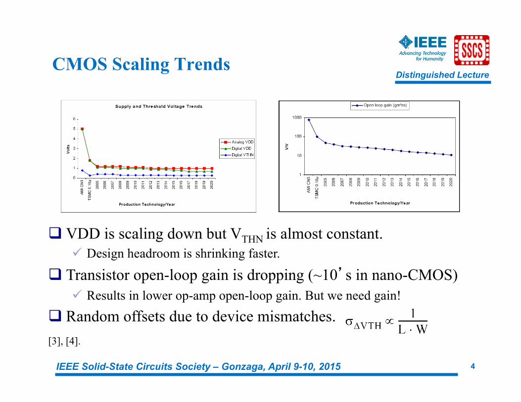
q VDD is scaling down but VTHN is almost constant. ü Design headroom is shrinking faster.
q Transistor open-loop gain is dropping (~10’s in nano-CMOS) ü Results in lower op-amp open-loop gain. But we need gain!
q Random offsets due to device mismatches. [3], [4].

Distinguished Lecture
IEEE Solid-State Circuits Society – Gonzaga, April 9-10, 2015 5
Integration of Analog into Nano-CMOS?
q Design low-VDD op-amps. ü Replace vertical stacking (cascoding) by horizontal cascading of gain
stages (see the next slide).
q Explore more effective op-amp compensation techniques. q Offset tolerant designs. q Also minimize power and layout area to keep up with the
digital trend. q Better power supply noise rejection (PSRR).

Distinguished Lecture
IEEE Solid-State Circuits Society – Gonzaga, April 9-10, 2015 6
Cascoding vs Cascading in Op-Amps A Telescopic Two-stage Op-Amp
A Cascade of low-VDD Amplifier Blocks.
(Compensation not shown here)
1
VDD VDD
Vbiasn
vp vm
VDD
CL
vout
2
VDD VDD
Vbiasn
VDD VDD
Vbiasn
n-1
n
Stage 1 Stage 2 Stage (n-1) Stage n
VDDmin>4Vovn+Vovp+VTHP with wide-swing biasing. [1]
VDDmin=2Vovn+Vovp+VTHP.
q Even if we employ wide-swing biasing for low-voltage designs, three- or higher stage op-amps will be indispensable in realizing large open-loop DC gain.

Distinguished Lecture
IEEE Solid-State Circuits Society – Gonzaga, April 9-10, 2015 7
TWO-STAGE OP-AMP COMPENSATION
Distinguished Lecture
IEEE Solid-State Circuits Society – Gonzaga, April 9-10, 2015 8
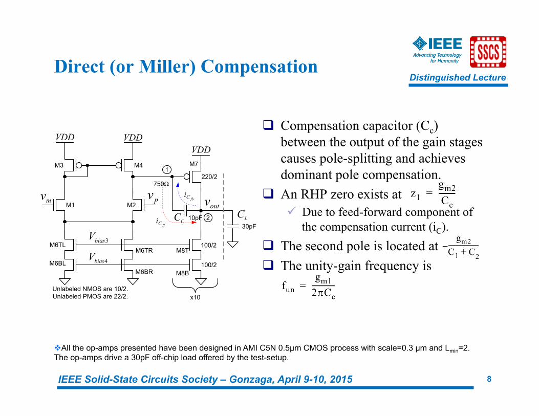
Direct (or Miller) Compensation
1
2
vm vp vout
Vbias4
Vbias3
CC 10pF
Unlabeled NMOS are 10/2.Unlabeled PMOS are 22/2.
VDD VDD VDD
30pF
CL
M3 M4
M1 M2
M6TL
M6BL
M6TR
M6BR
M8T
M8B
M7
220/2
100/2
100/2
x10
750Ω
iC fb
iC ff
q Compensation capacitor (Cc) between the output of the gain stages causes pole-splitting and achieves dominant pole compensation.
q An RHP zero exists at ü Due to feed-forward component of
the compensation current (iC). q The second pole is located at q The unity-gain frequency is
v All the op-amps presented have been designed in AMI C5N 0.5µm CMOS process with scale=0.3 µm and Lmin=2. The op-amps drive a 30pF off-chip load offered by the test-setup.
Distinguished Lecture
IEEE Solid-State Circuits Society – Gonzaga, April 9-10, 2015 9
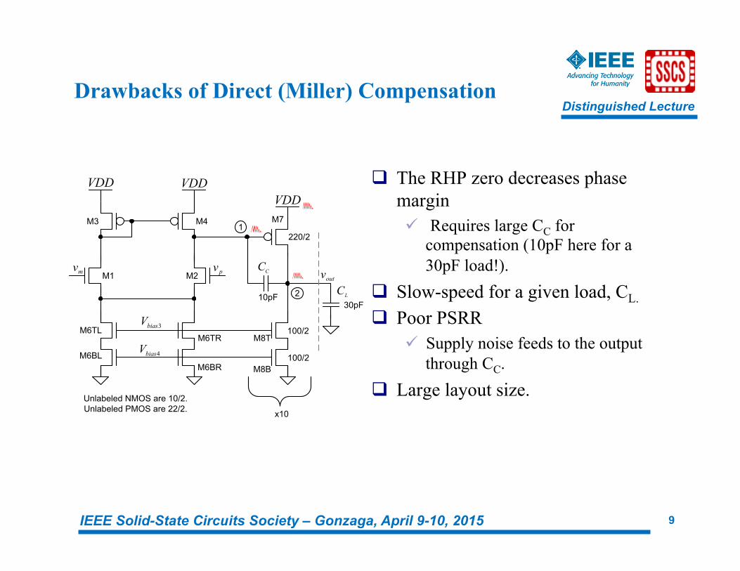
Drawbacks of Direct (Miller) Compensation
q The RHP zero decreases phase margin ü Requires large CC for
compensation (10pF here for a 30pF load!).
q Slow-speed for a given load, CL.
q Poor PSRR ü Supply noise feeds to the output
through CC. q Large layout size.
1
2
vm vp vout
Vbias4
Vbias3
CC
10pF
Unlabeled NMOS are 10/2.Unlabeled PMOS are 22/2.
VDD VDD VDD
30pFCL
M3 M4
M1 M2
M6TL
M6BL
M6TR
M6BR
M8T
M8B
M7
220/2
100/2
100/2
x10
Distinguished Lecture
IEEE Solid-State Circuits Society – Gonzaga, April 9-10, 2015 10
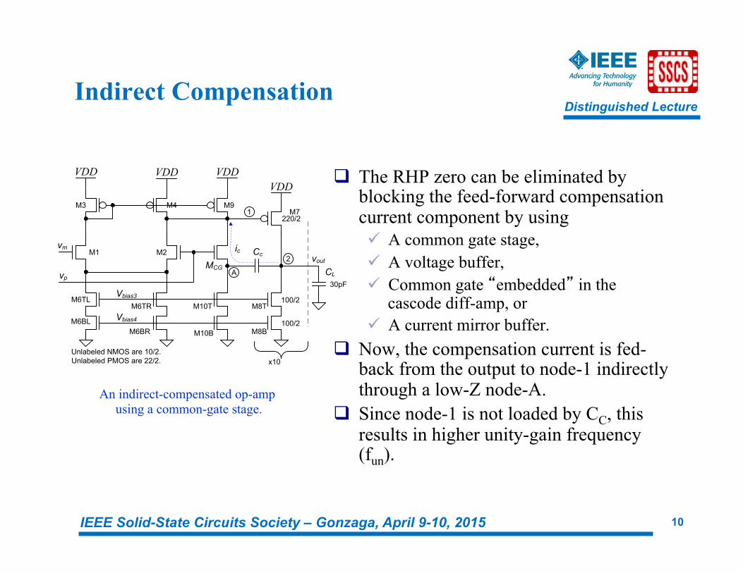
Indirect Compensation
q The RHP zero can be eliminated by blocking the feed-forward compensation current component by using ü A common gate stage, ü A voltage buffer, ü Common gate “embedded” in the
cascode diff-amp, or ü A current mirror buffer.
q Now, the compensation current is fed-back from the output to node-1 indirectly through a low-Z node-A.
q Since node-1 is not loaded by CC, this results in higher unity-gain frequency (fun).
An indirect-compensated op-amp using a common-gate stage.
1
2
Unlabeled NMOS are 10/2.Unlabeled PMOS are 22/2.
VDD VDD VDD
30pF
220/2
100/2
100/2
x10
VDD
Vbias3
Vbias4
vm
vp
voutCc
CL
ic
MCGA
M3 M4
M1
M6TL
M6BL
M6TR
M6BR
M8T
M8B
M7
M2
M9
M10T
M10B
Distinguished Lecture
IEEE Solid-State Circuits Society – Gonzaga, April 9-10, 2015 11
Indirect Compensation in a Cascoded Op-Amp
1
2
vm vp voutCC
1.5pF
Unlabeled NMOS are 10/2.Unlabeled PMOS are 44/2.
VDD VDD
VDD
30pFCL
Vbias2
Vbias3
Vbias4
A
50/2
50/2
110/2
M1 M2
M6TL
M6BL
M6TR
M6BR
M3T
M3B
M4T
M4B
M8T
M8B
M7
ic
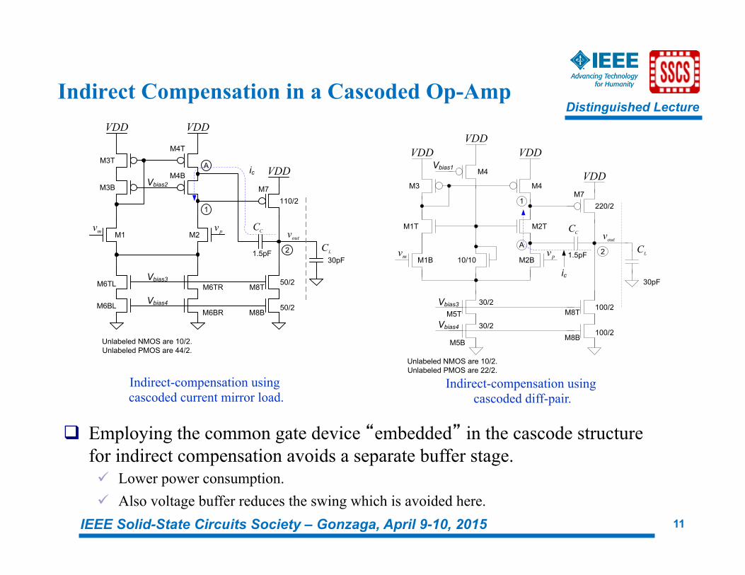
Indirect-compensation using cascoded current mirror load.
1
2vm vp
voutCC
1.5pF
Unlabeled NMOS are 10/2.Unlabeled PMOS are 22/2.
VDD VDD
VDD
30pF
CL
Vbias3
Vbias4
A
100/2
100/2
220/2
M1B M2B
M5T
M5B
M3
M1T
M4
M2T
M8T
M8B
M7
VDD
M4Vbias1
30/2
30/2
10/10
ic
Indirect-compensation using cascoded diff-pair.
q Employing the common gate device “embedded” in the cascode structure for indirect compensation avoids a separate buffer stage. ü Lower power consumption. ü Also voltage buffer reduces the swing which is avoided here.
Distinguished Lecture
IEEE Solid-State Circuits Society – Gonzaga, April 9-10, 2015 12
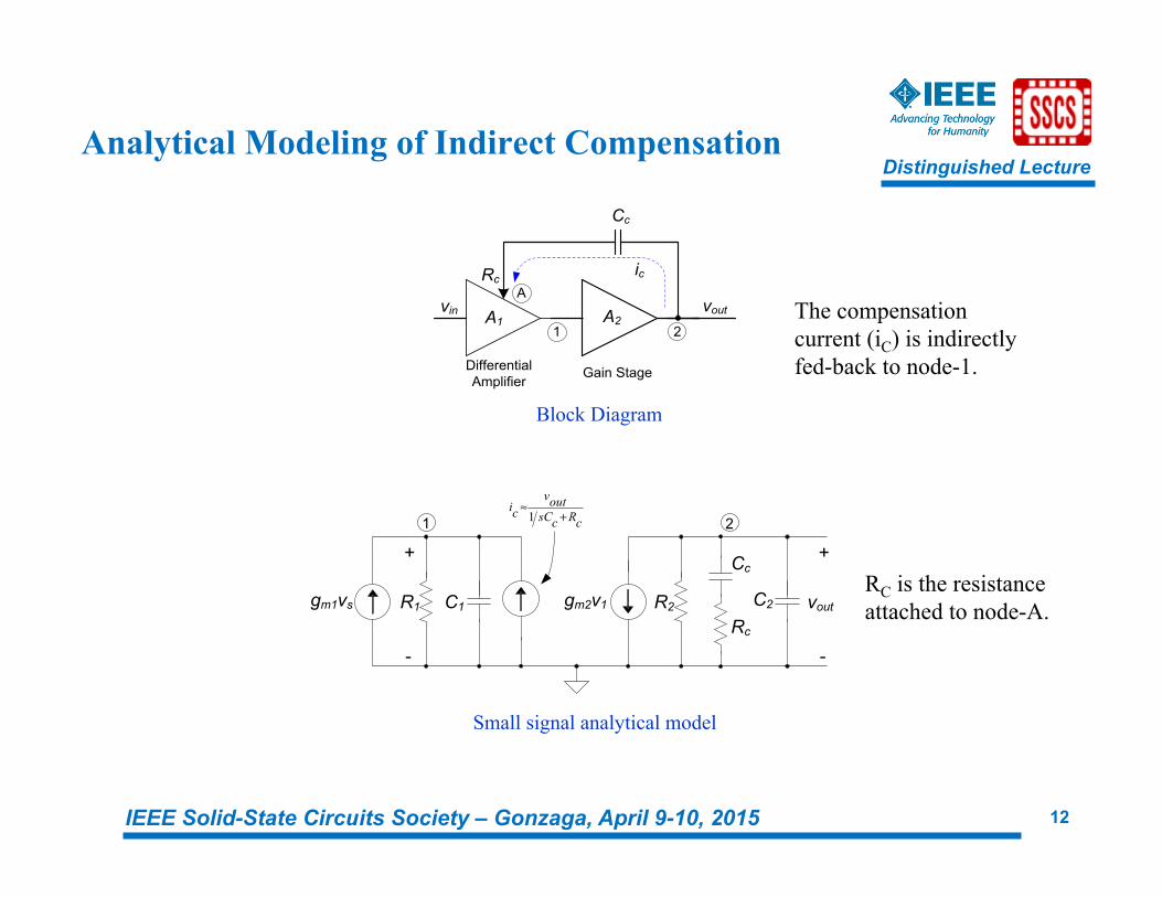
Analytical Modeling of Indirect Compensation
A1 A2
Cc
1 2
vin vout
DifferentialAmplifier Gain Stage
RcA
ic
Block Diagram
Small signal analytical model
RC is the resistance attached to node-A.
icvoutsCc Rc
≈+1
+
-
+
-
1 2
gm1vs gm2v1R1 C1 R2 C2 vout
Cc
Rc
The compensation current (iC) is indirectly fed-back to node-1.
Distinguished Lecture
IEEE Solid-State Circuits Society – Gonzaga, April 9-10, 2015 13
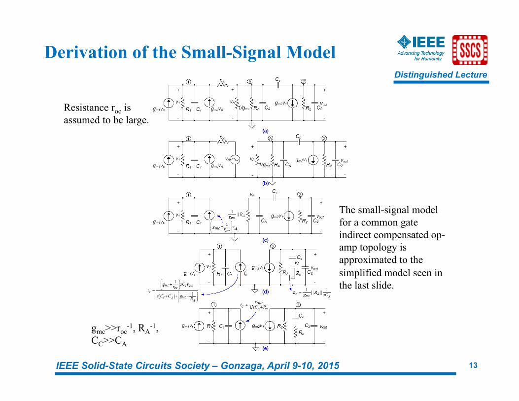
Derivation of the Small-Signal Model
The small-signal model for a common gate indirect compensated op-amp topology is approximated to the simplified model seen in the last slide.
Resistance roc is assumed to be large.
gmc>>roc-1, RA
-1, CC>>CA

Distinguished Lecture
IEEE Solid-State Circuits Society – Gonzaga, April 9-10, 2015 14
Analytical Results for Indirect Compensation
jω
σz1
−ω un
p1p2p3
Pole-zero plot
q Pole p2 is much farther away from fun. ü Can use smaller gm2=>less power!
q LHP zero improves phase margin. q Much faster op-amp with lower
power and smaller CC. q Better slew rate as CC is smaller.
LHP zero

Distinguished Lecture
IEEE Solid-State Circuits Society – Gonzaga, April 9-10, 2015 15
Indirect Compensation Using Split-Length Devices
q As VDD scales down, cascoding is becoming tough. Then how to realize indirect compensation as we have no low-Z node available?
q Solution: Employ split-length devices to create a low-Z node. ü Creates a pseudo-cascode stack but its really a single device.
q In the NMOS case, the lower device is always in triode hence node-A is a low-Z node. Similarly for the PMOS, node-A is low-Z.
A
VDD M1T
W/L1
M1BW/L2
M1W/(L1+L2)
Equivalent
M1T
W/L1
M1BW/L2
M1W/(L1+L2)
VDD Triode
Triode
Low-Z node
Low-Z node
EquivalentA
NMOS PMOS Split-length 44/4(=22/2)
PMOS layout
S
D
A
Low-Z node
G
Distinguished Lecture
IEEE Solid-State Circuits Society – Gonzaga, April 9-10, 2015 16
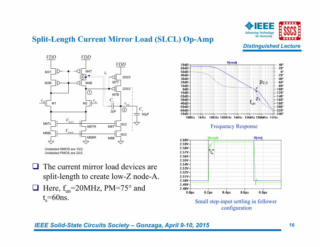
Split-Length Current Mirror Load (SLCL) Op-Amp
1
2
vm vp vout
Vbias4
Vbias3
CC
2pF
Unlabeled NMOS are 10/2.Unlabeled PMOS are 22/2.
VDD VDD VDD
30pFCL
M3B M4B
M1 M2
M6TL
M6BL
M6TR
M6BR
M8T
M8B
M7T
M3T M4T
M7B
50/2
50/2
220/2
220/2
Aic
funz1
p2,3
q The current mirror load devices are split-length to create low-Z node-A.
q Here, fun=20MHz, PM=75° and ts=60ns.
ts
Frequency Response
Small step-input settling in follower configuration
Distinguished Lecture
IEEE Solid-State Circuits Society – Gonzaga, April 9-10, 2015 17
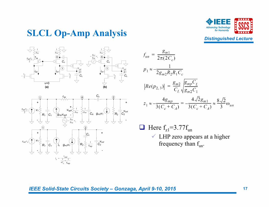
SLCL Op-Amp Analysis
12vout
A
1gmp
id1id2vs2
1gmp
gm vs12
+-
−vs2
CL
Cc
v=0
12vout
A
1gmp
id1vs2
CL
Cc
−gg vm
mp s1
(a) (b)
+
-
+
-
1 2
gm2v1R1 C1vout
Cc
v1
rop
CA
+
-vsgA
C2R2
A
−gg vm
mp s1
1gmp
gmpvsgA
icvout
sCc gmp
≈+1 1
+
-
+
-
1 2
gm2v1R1 C1vout
Cc
v1C2R2ic
gm vs1 1gmp
gm vs12
1gmp
q Here fz1=3.77fun ü LHP zero appears at a higher
frequency than fun.
Distinguished Lecture
IEEE Solid-State Circuits Society – Gonzaga, April 9-10, 2015 18
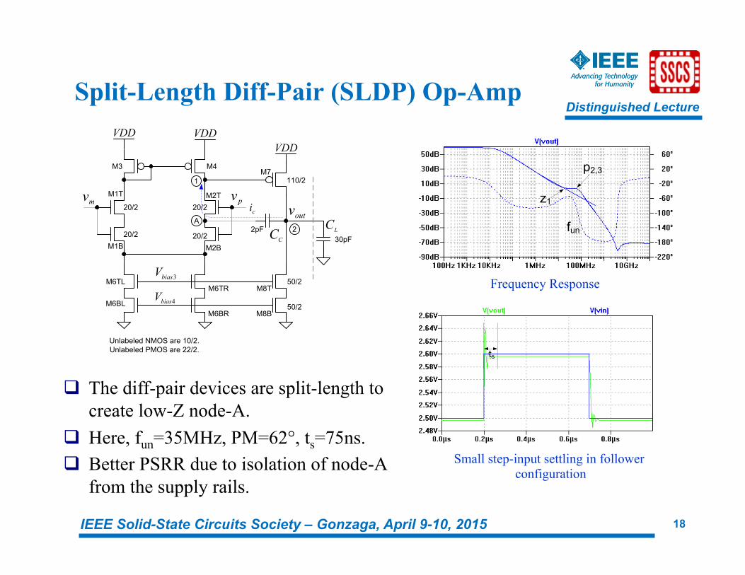
Split-Length Diff-Pair (SLDP) Op-Amp
q The diff-pair devices are split-length to create low-Z node-A.
q Here, fun=35MHz, PM=62°, ts=75ns. q Better PSRR due to isolation of node-A
from the supply rails.
Frequency Response
Small step-input settling in follower configuration
1
2
vm vpvout
Vbias4
Vbias3
CC2pF
Unlabeled NMOS are 10/2.Unlabeled PMOS are 22/2.
VDD VDD VDD
30pF
CL
M3 M4
M1B M2B
M6TL
M6BL
M6TR
M6BR
M8T
M8B
M7
M1T M2T20/2
20/2
20/2
20/2
ic
110/2
50/2
50/2
A fun
p2,3
z1
ts

Distinguished Lecture
IEEE Solid-State Circuits Society – Gonzaga, April 9-10, 2015 19
SLDP Op-Amp Analysis
12vout
A
id1id2vs2
−vs2
CL
Cc
v=0
1gmn
1gmn
12vout
A
id2 vs2
CL
Cc1gmn
rop
(a) (b)
idgmnvs
2 4= −
q Here fz1=0.94fun, ü LHP zero appears slightly before
fun and flattens the magnitude response.
ü This may degrade the phase margin.
q Not as good as SLCL, but is of great utility in multi-stage op-amp design due to higher PSRR.
+
-
+
-
1 2
gm2v1CAvoutvA
ron
C1
+
-vgs1
C2R2
A
gmnvgs1vs2
1gmn R1gmnvs
4
Cc
1gmn
icvout
sCc gmn
≈+1 1
+
-
+
-
1 2
gm2v1R1 C1vout
Cc
v1C2R2ic
gmnvs2 1
gmn

Distinguished Lecture
IEEE Solid-State Circuits Society – Gonzaga, April 9-10, 2015 20
Test Chip 1: Two-stage Op-Amps
Miller 3-Stage Indirect
SLCL Indirect
SLDP Indirect
Miller with Rz
q AMI C5N 0.5µm CMOS, 1.5mmX1.5mm die size.
Distinguished Lecture
IEEE Solid-State Circuits Society – Gonzaga, April 9-10, 2015 21
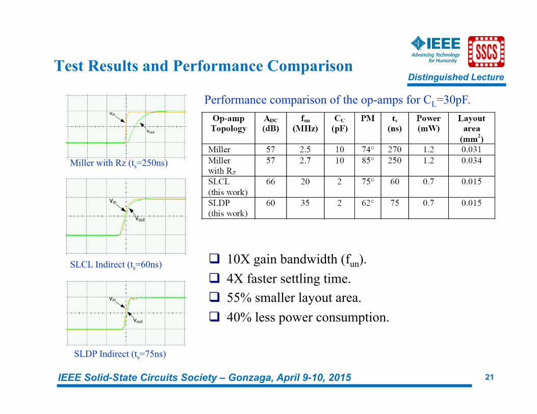
Test Results and Performance Comparison
vin
vout
vin
vout
vin
vout
Miller with Rz (ts=250ns)
SLCL Indirect (ts=60ns)
SLDP Indirect (ts=75ns)
Performance comparison of the op-amps for CL=30pF.
q 10X gain bandwidth (fun). q 4X faster settling time. q 55% smaller layout area. q 40% less power consumption.

Distinguished Lecture
IEEE Solid-State Circuits Society – Gonzaga, April 9-10, 2015 22
MULTI-STAGE OP-AMP DESIGN

Distinguished Lecture
IEEE Solid-State Circuits Society – Gonzaga, April 9-10, 2015 23
Three-Stage Op-Amps
q Higher gain can be achieved by cascading three gain stages. ü ~100dB in 0.5µm CMOS
q Results in at least a third order system ü 3 poles and two zeros. ü RHP zero(s) degrade the phase
margin. q Hard to compensate and stabilize. q Large power consumption compared
to the two-stage op-amps.
zLHP
s plane
jω
σp1p2,3
zRHP
−ωun
Clustered non-dominant poles
Pole-zero plot

Distinguished Lecture
IEEE Solid-State Circuits Society – Gonzaga, April 9-10, 2015 24
Biasing of Multi-Stage Op-Amps
1
VDD VDD
Vbiasn
vp vm
~Vbiasp
Vbiasp
M1 M2
M3L M3R
M4 M5
3
VDD
CL
vout
M12
M11
2
VDD VDD
Vbiasn
~Vbiasp Vbiasp
M6 M7
M8L M8R
M9 M10Current flowing in this branch is set
by Vbiasp.
q Diff-amps should be employed in inner gain stages to properly bias second and third gain stages ü Current in third stage is
precisely set. ü Robust against large offsets. ü Boosts the CMRR of the op-
amp (needed). q Common source second stage
should be avoided. ü Will work in feedback
configuration but will have offsets in nano-CMOS processes.
1
VDD VDD VDD
Vbiasn
vp vm
2
~Vbiasp
Vbiasp
Unknown Voltage level, can move up or down.
M1 M2
M3L M3R
M4 M5M6
M7
3
VDD
CL
vout
Current in this branch is unknownM8
M9
Robust Biasing
Fallible Biasing

Distinguished Lecture
IEEE Solid-State Circuits Society – Gonzaga, April 9-10, 2015 25
Conventional Three-Stage Topologies
1
2
VDD VDD VDD VDD VDD VDD
CL
vm vp voutCc1
Cc2
Rc
VB1
VB2
VB4VB5
VB3gm1
gm2
gm3
3
40uA
10uA 10uA
10uA
10uA
100uA
100pF
q Requires p3=2p2=4ωun for stability (Butterworth response) ü Huge power consumption
q RHP zero appears before the LHP zero and degrades the phase margin.
q Second stage is non-inverting ü Implemented using a current
mirror. ü Excess forward path delay (not
modeled or discussed in the literature).
-A1 +A2
Cc1
1 2
vs vout -A33
Cc2
Nested Miller Compensation (NMC) [6]

Distinguished Lecture
IEEE Solid-State Circuits Society – Gonzaga, April 9-10, 2015 26
Conventional Three-Stage Topologies contd.
gm1 +gm2
Cc1
1vs vout -gm3
Cc2
2 3
-gmf1
-gmf2
q Employs feed-forward gm’s to eliminate zeros. ü gmf1=gm1 and gmf2=gm2
q Class AB output stage. q Hard to implement gmf1 which
tracks gm1 for large signal swings. ü Also wasteful of power.
q gmf2 is a power device and will not always be equal to gm2. ü Compensation breaks down.
q Still consumes large power.
Nested Gm-C Compensation (NGCC) [7]
1
2
3
VDD
vm vpgm1
VDD VDD VDD VDD
VB1
VDD
20uA
Cc1
VB2
CL
voutCc2
gm2gmf1
gm3
gmf224/3
60/3
120/3 180/3120/3
24/3 24/3
48/3
48/3
120/3
48/3
420/3
24/3
20uA 70uA

Distinguished Lecture
IEEE Solid-State Circuits Society – Gonzaga, April 9-10, 2015 27
Conventional Three-Stage Topologies contd.
q Four poles and double LHP zeros ü One LHP zero z1 cancels the pole p3.
ü Other LHP zero z2 enhances phase margin.
q Set p2=2ωun for PM=60°. q Relatively low power. q Still design criterions are complex. q Complicated bias circuit.
ü More power. q Excess forward path delay.
Transconductance with Capacitive Feedback Compensation (TCFC) [14]
1
2
VDD VDD VDD VDD VDD VDD
vm vp
vout
CC2
VB1
VB3
VB7
VB2gm1
gm3
3
gm2/2gmf
VB4
VB5
1:2
VB6gmt
CC1
-A1 +A21 2
vs vout -A33
CC2
-gmf
+gmt
CC1

Distinguished Lecture
IEEE Solid-State Circuits Society – Gonzaga, April 9-10, 2015 28
Three-Stage Topologies: Latest in the literature
q Employs reverse nesting of compensation capacitors ü Since output is only loaded by only
CC2, results in potentially higher fun. ü Third stage is always non-inverting.
q Uses pole-zero cancellation to realize higher phase margins.
q Excess forward path delay. q Biasing not robust against process
variations. How do you control the current in the output buffer?
Reverse Nested Miller with Voltage Buffer and Resistance (RNMC-VBR) [8]
-A1 -A2
Cc1
1 2
vs vout +A33
Cc2
Rc2
Rc1CG
1
VDD
vm vpgm1
VDD
20uA
23
VDD VDD VDD VDD
vout
CL
Cc1
Cc2
gm2
gm3
gmf
gmVB
RC1
Distinguished Lecture
IEEE Solid-State Circuits Society – Gonzaga, April 9-10, 2015 29
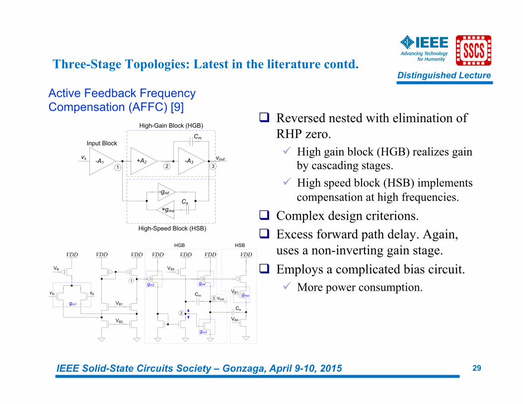
Three-Stage Topologies: Latest in the literature contd.
q Reversed nested with elimination of RHP zero. ü High gain block (HGB) realizes gain
by cascading stages. ü High speed block (HSB) implements
compensation at high frequencies. q Complex design criterions. q Excess forward path delay. Again,
uses a non-inverting gain stage. q Employs a complicated bias circuit.
ü More power consumption.
Active Feedback Frequency Compensation (AFFC) [9]
-A1 +A2
Ca
1 2
vs vout -A33
Cm
-gmf
+gma
High-Gain Block (HGB)
High-Speed Block (HSB)
Input Block
1
2
VDD VDD VDD VDD VDD VDD
vm vp vout
Cm
VB
VB2
VB5
VB1gm1
gm3
3
gm2 gmf
VDD
VB1
VB4
Ca
gma
HGB HSB
Distinguished Lecture
IEEE Solid-State Circuits Society – Gonzaga, April 9-10, 2015 30
Three-Stage Topologies: Latest in the literature contd.
q Various topologies have been recently reported by combining the earlier techniques. ü RNMC feed-forward with nulling resistor (RNMCFNR) [17]. ü Reverse active feedback frequency compensation (RAFFC) [17].
q Further improvements are required in ü Eliminating excess forward path delay arising due to the compulsory non-
inverting stages. ü Robust biasing against random offsets in nano-CMOS. ü Further reduction in power and circuit complexity. ü Better PSRR.

Distinguished Lecture
IEEE Solid-State Circuits Society – Gonzaga, April 9-10, 2015 31
Indirect Compensation in Three-Stage Op-Amps
q Indirectly feedback the compensation currents ic1 and ic2. ü Reversed Nested
q Thus named RNIC.
q Employ diff-amp stages for robust biasing and higher CMRR.
q Use SLDP for higher PSRR. q Minimum forward path delay. q No compulsion on the polarity of gain
stages. ü Can realize any permutation of stage
polarities by just changing the sign of the fed-back compensation current using ‘fbr’ and ‘fbl’ nodes.
q Low-voltage design. q Note Class A (we’ll modify after
theory is discussed).
-A1 +A2
Cc1
1 2
vs voutic1
-A33
Cc2
ic2-
+
VDD VDD VDD
Vbiasn
vpfbl fbr
Cc2
CL
vm
VDD VDD
voutCc1
fbl
fbr
+ve
-ve
ic1
ic2
1
2
3

Distinguished Lecture
IEEE Solid-State Circuits Society – Gonzaga, April 9-10, 2015 32
Indirect Compensation in Three-Stage Op-Amps contd.
VDD VDD VDD
Vbiasn
vpfbl fbr
Cc2
CL
vm
VDD VDD
voutCc1
fbl
fbr
+ve
-ve
ic1
ic2
1
2
3
q Note the red arrows showing the node movements and the signs of the compensation currents. ü fbr and fbl are the low-Z nodes used for indirect compensation (have
resistances Rc1 and Rc2 attached to them). q The CC’s are connected across two-nodes which move in opposite
direction for overall negative feedback the compensation loops. q Note feedback and forward delays!

Distinguished Lecture
IEEE Solid-State Circuits Society – Gonzaga, April 9-10, 2015 33
Analysis of the Indirect Compensated 3-Stage Op-Amp
iv
sCc Rc c12
1 11≈ +
+
-
+
-
1 2
gm1vs gm2v1R1 C1 R2
C2v2
Cc1
Rc1
v1
+
-
3
gm3v2 R3
C3 vout
Cc2
Rc2
iv
sC Rcout
c c2 2 21≈ +
ic1 ic2
Two LHP zeros Four non-dominant poles.
q Plug in the indirect compensation model developed for the two-stage op-amps.

Distinguished Lecture
IEEE Solid-State Circuits Society – Gonzaga, April 9-10, 2015 34
Pole-zero Cancellation q Poles p4,5 are parasitic conjugated poles located far away in frequency.
ü Appear due to the loading of the nodes fbr and fbl.
q The small signal transfer function can be written as
q The quadratic expression in the denominator describing the poles p2 and p3 can be canceled by the numerator which describes the LHP zeros. ü Results in LHP zeros z1 and z2 canceling the poles p2 and p3 resp.
q The resulting expression looks like a single pole system for low frequencies. →Phase margin close to 90°.

Distinguished Lecture
IEEE Solid-State Circuits Society – Gonzaga, April 9-10, 2015 35
Pole-zero Cancellation contd.
s plane
jω
σp1
p2,z1−ωun
p3,z2
Non-dominant pole zero doublets
p4,5
Design Equations
q Place pole-zero doublets (p2-z1 and p3-z2) out of fun for clean transients. ü i.e. fp2, fp3 > fun.
q Best possible pole-zero arrangement for low power design.
q Results into design equations independent of parasitics (C3≈CL here).
q Rc1 and Rc2 are realized by adding poly R’s in series with CC1 and CC2. ü Also Rc1, Rc2≥Rc0, the impedance
attached to the low-Z nodes fbr/fbl. q Robust against even 50% process
variations in R’s and C’s as long as the pole-zero doublets stay out of fun.

Distinguished Lecture
IEEE Solid-State Circuits Society – Gonzaga, April 9-10, 2015 36
Pole-zero cancelled Class-A Op-Amp
Unlabeled NMOS are 10/2.Unlabeled PMOS are 22/2.
VDD VDD VDD
30pF
20/2
20/2
20/2
20/2
Vbiasn
vpfbl fbr
220/2
100/2
CL
vm
VDD VDD
vout
1
2
3
M4 M5
M1T
M1B
M2T
M2B
M3L M3R M7L M7R
M8 M9
M5 M6
M10
M11
Cc2fbr
R2c
Cc1
fblR1c
30/2 30/2
7.65K
4.08K
1p
2p
q A Here, the poly resistors are estimated as
q Low power, simple, robust and manufacturable topology*. v The presented three-stage op-amps have been designed with transient and SR performances to
be comparable to their two-stage counterparts.

Distinguished Lecture
IEEE Solid-State Circuits Society – Gonzaga, April 9-10, 2015 37
Pole-zero cancelled Class-AB Op-Amp 1
q A dual-gain path, low-power Class-AB op-amp topology (RNIC-1).
q The design equation for Rc1 is modified as
Unlabeled NMOS are 10/2.Unlabeled PMOS are 22/2.
VDD VDD
VDD
30pF
20/2
20/2
20/2
20/2
Vbiasn
vpfbl fbr
220/2
100/2
Cc2 CL
vm
VDD VDD
vout
Cc1
fblfbr
1
2
3
M4 M5
M1T
M1B
M2T
M2B
M3L M3R M7L M7R
M8 M9
M5 M6
M10
M11
R1cR2c
Vbiasp
66/2 66/2
124 1p 2p1.14K
Distinguished Lecture
IEEE Solid-State Circuits Society – Gonzaga, April 9-10, 2015 38
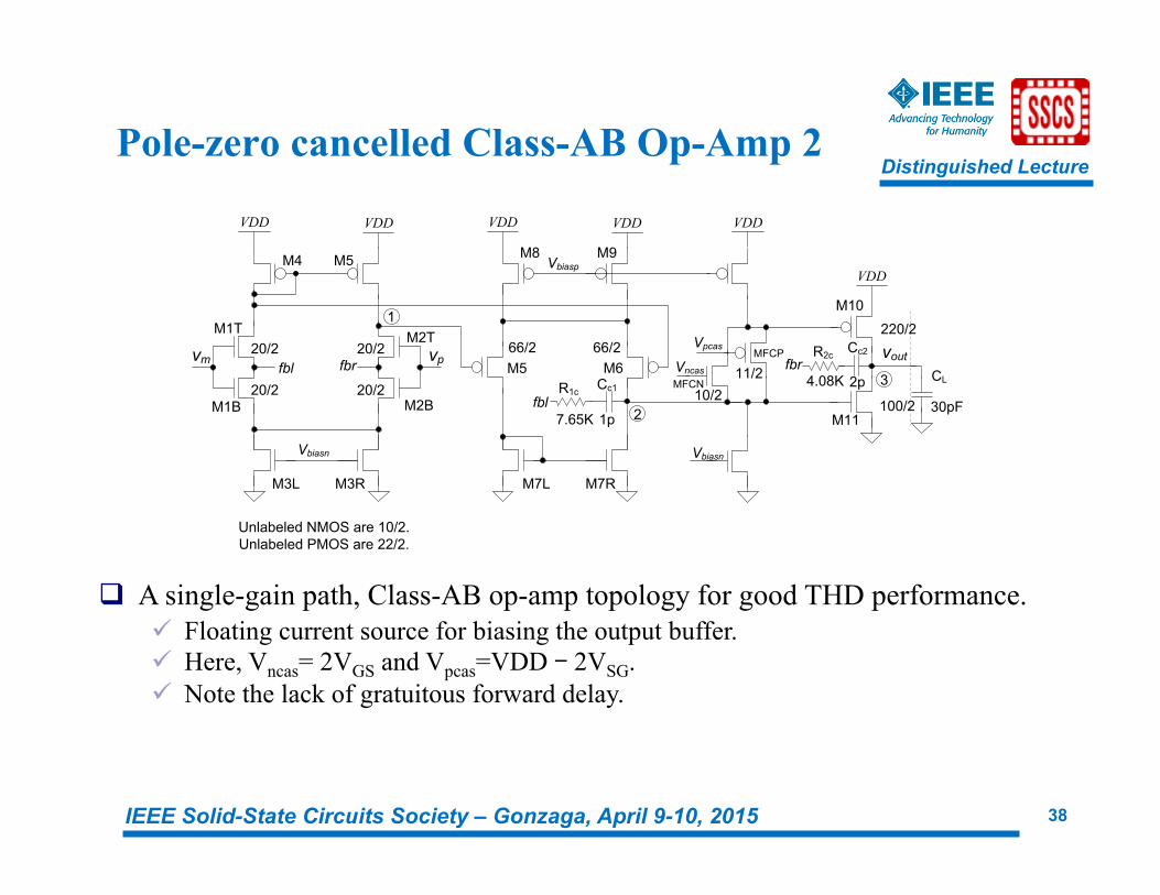
Pole-zero cancelled Class-AB Op-Amp 2
q A single-gain path, Class-AB op-amp topology for good THD performance. ü Floating current source for biasing the output buffer. ü Here, Vncas= 2VGS and Vpcas=VDD - 2VSG. ü Note the lack of gratuitous forward delay.
Unlabeled NMOS are 10/2.Unlabeled PMOS are 22/2.
VDD VDD
VDD
30pF
20/2
20/2
20/2
20/2
Vbiasn
vpfbl fbr
220/2
100/2
CL
vm
VDD VDD
vout
1
2
3
M4 M5
M1T
M1B
M2T
M2B
M3L M3R M7L M7R
M8 M9
M5 M6
M10
M11
Vbiasp
66/2 66/2
Vbiasn
VDD
Vpcas
Vncas
10/211/2
MFCP
MFCNCc1
fblR1c
Cc2fbr
R2c
7.65K
4.08K
1p
2p
Distinguished Lecture
IEEE Solid-State Circuits Society – Gonzaga, April 9-10, 2015 39
Simulation of Three-stage Op-Amps
-150
-100
-50
0
50
100
Mag
nitud
e (d
B)
102 104 106 108 1010-225
-180
-135
-90
-45
0
Phas
e (d
eg)
Bode Diagram
Frequency (Hz)
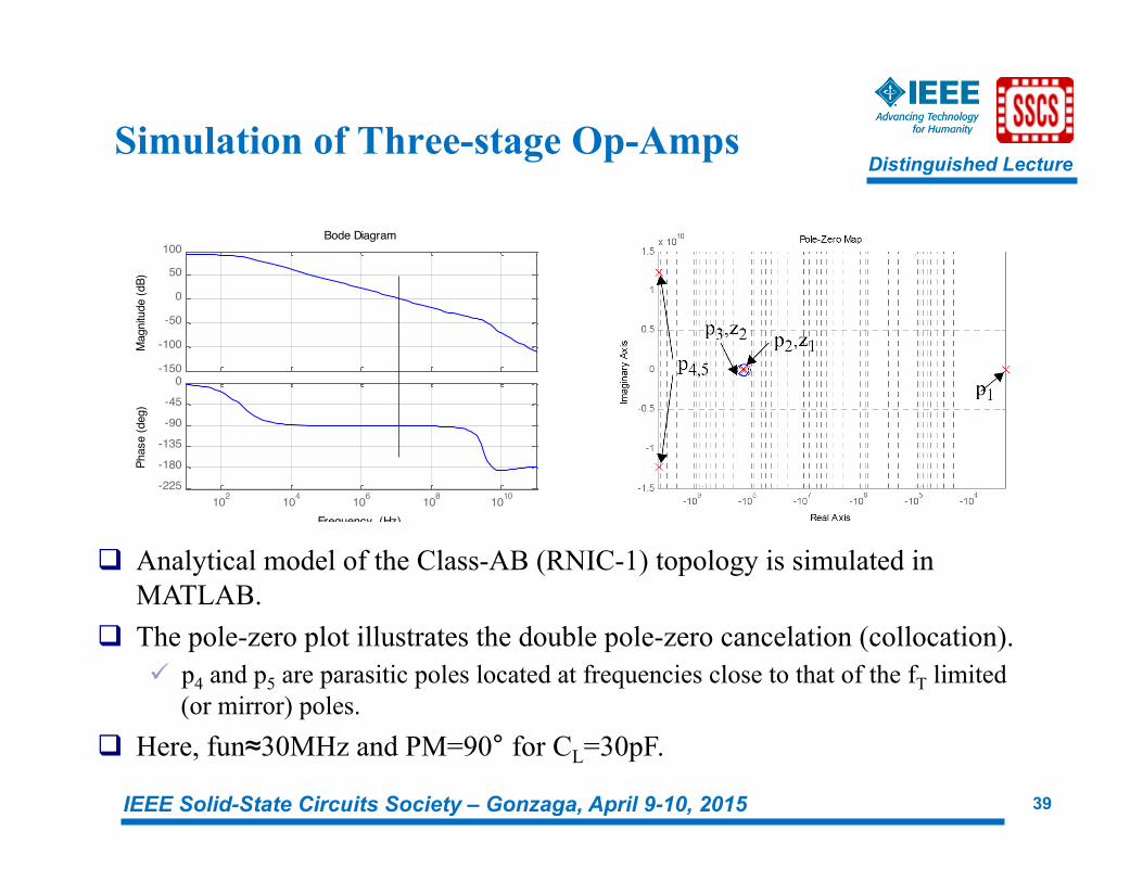
q Analytical model of the Class-AB (RNIC-1) topology is simulated in MATLAB.
q The pole-zero plot illustrates the double pole-zero cancelation (collocation). ü p4 and p5 are parasitic poles located at frequencies close to that of the fT limited
(or mirror) poles. q Here, fun≈30MHz and PM=90° for CL=30pF.
Distinguished Lecture
IEEE Solid-State Circuits Society – Gonzaga, April 9-10, 2015 40
Simulation of Three-stage Op-Amps contd.
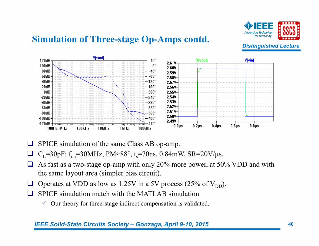
q SPICE simulation of the same Class AB op-amp. q CL=30pF: fun=30MHz, PM≈88°, ts=70ns, 0.84mW, SR=20V/µs. q As fast as a two-stage op-amp with only 20% more power, at 50% VDD and with
the same layout area (simpler bias circuit). q Operates at VDD as low as 1.25V in a 5V process (25% of VDD). q SPICE simulation match with the MATLAB simulation
ü Our theory for three-stage indirect compensation is validated.
Distinguished Lecture
IEEE Solid-State Circuits Society – Gonzaga, April 9-10, 2015 41
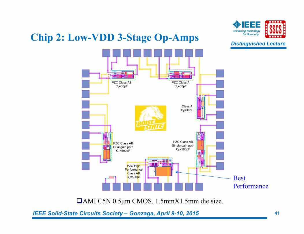
Chip 2: Low-VDD 3-Stage Op-Amps
PZC Class AB CL=30pF
PZC Class A CL=30pF
Class A CL=30pF
PZC Class AB Dual gain path
CL=500pF
PZC Class AB Single gain path
CL=500pF
PZC High Performance
Class AB CL=500pF Best
Performance
q AMI C5N 0.5µm CMOS, 1.5mmX1.5mm die size.

Distinguished Lecture
IEEE Solid-State Circuits Society – Gonzaga, April 9-10, 2015 42
Performance Comparison
q Figures of Merit ü FoMS=funCL/Power ü FoML=SR.CL/Power ü IFoMS=funCL/IDD
ü IFoML=SR.CL/IDD
q RNIC op-amp designed for 500pF load for a fair comparison.
q FoMs>2X than state-of-the-art at VDD=3V.
q Comparable performance even at lower VDD=2V.
q Practical, stable and production worthy.
Distinguished Lecture
IEEE Solid-State Circuits Society – Gonzaga, April 9-10, 2015 43
Performance Comparison contd.
0
10000
20000
30000
40000
50000
60000
MNMCNGCC
NMCFNR
DFCFCAFFC
ACBCFTCFC
DPZCF
RNMC VB NR
SMFFC
RNMCFNR
RAFFC
RAFFC LP
RNIC-2
(This w
ork)
RNIC-3
(This w
ork)
RNIC-2A
(This
work
)
RNIC-3A
(This
work
)
FOM_S
FOM_L
IFOM_S
IFOM_L
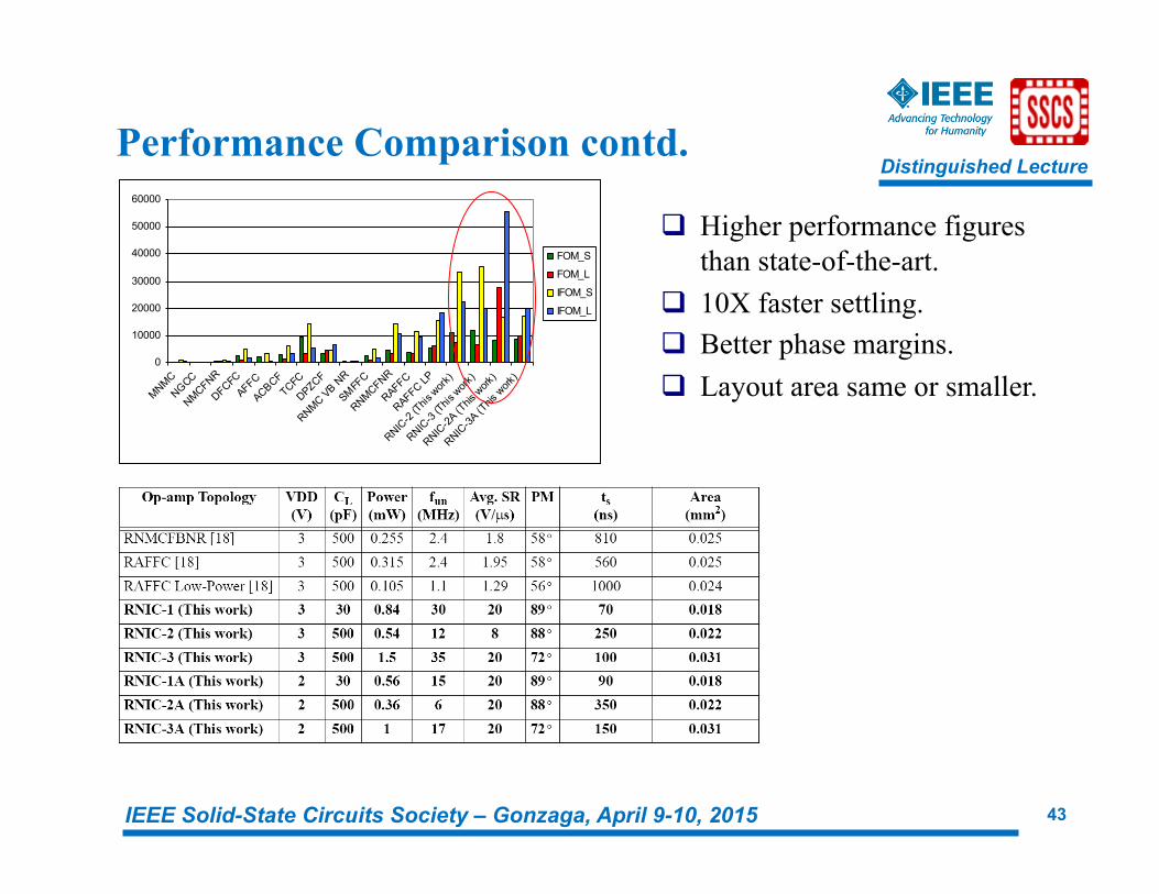
q Higher performance figures than state-of-the-art.
q 10X faster settling. q Better phase margins. q Layout area same or smaller.

Distinguished Lecture
IEEE Solid-State Circuits Society – Gonzaga, April 9-10, 2015 44
Flowchart for RNIC Op-Amp Design Start with the initial
specifications on fun, CL, Av, and SR.
Select the overdrive (% of VDD) which will set VGS, fT and transistor gain gm*ro.
Identify gm1. Can initially set gm2 equal to gm1 or a to lower value.
Select Cc2 = gm1/fun
Select Cc1 and gm3 such that the p2-z1 and p3-z2 doublet locations are outside fun.
Calculate R1c and R2c.
Is either of R1c and R2c negative?
Are the parasitic poles p4,5 degrading
PM by closing on fun?
Simulate the design for frequency response
and transient settling.
Does the design meet the
specifications?
No
Lower power?
Smaller layout area?
More Speed?
Better SR?
Split DC gain AOLDC across A1, A2 and A3.
Move the corresponding pi-zj doublet to a lower frequency by changing Cci and Rci. May
have to sacrifice fun.
Yes
End
Yes
Increase gm1 or decrease Cc2.
Yes
No
Decrease gm3 or gm2. In the worst case
scenario decrease gm1.
Yes
No
Reduce Cc1, Cc2 or gm3.
Yes
No
Increase bias current in the first stage (i.e. ISS1) or use
smaller CC’sYesNothing works!
Revisit biasing. No
Increase gm2.Yes
No
No

Distinguished Lecture
IEEE Solid-State Circuits Society – Gonzaga, April 9-10, 2015 45
N-Stage Indirect Compensation Theory
A1 -A21 2
vs vout -A33
+-
-An-1 -Ann-1 n
Cc1
Cc2
Ccn−2
Ccn−1
ic1ic2
icn−1icn−2
q The three-stage indirect compensation theory has been extended to N-stages and the closed form small signal transfer function is obtained.
Distinguished Lecture
IEEE Solid-State Circuits Society – Gonzaga, April 9-10, 2015 46
MULTI-STAGE FULLY-DIFFERENTIAL OP-AMPS

Distinguished Lecture
IEEE Solid-State Circuits Society – Gonzaga, April 9-10, 2015 47
Fully Differential Op-Amps
q Analog signal processing uses ‘only’ fully differential (FD) circuits. ü Cancels switch non-linearities and even
order harmonics. ü Double the dynamic range.
q Needs additional circuitry to maintain the output common-mode level. ü Common-mode feedback circuit
(CMFB) is employed.
CMFB
Vref
VCMFB
CL
CLvinm
vinp
vop
vom
vop-vom=-A(vinp-vinm)
Distinguished Lecture
IEEE Solid-State Circuits Society – Gonzaga, April 9-10, 2015 48
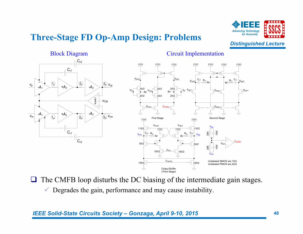
Three-Stage FD Op-Amp Design: Problems
-A1 +A2
Cc1
vp vop -A3
Cc2
-+ 1p 2p 3p
-A1 +A2
Cc1
vm vom -A3
Cc2
-+ 1m 2m 3m
CMFB vCM
q The CMFB loop disturbs the DC biasing of the intermediate gain stages. ü Degrades the gain, performance and may cause instability.
Unlabeled NMOS are 10/2.Unlabeled PMOS are 22/2.
VDD VDD
20/2
20/2
20/2
20/2
Vbiasn
vpfbl fbr
vm
VDD
20/2
20/2
VCM
vop1vom1
VCMFB1
VDD
vomCc2
fblR2c
110/2
100/2
50/2
VCMFB3
VDD
VDD
vopCc2
fbrR2c
110/2
100/2
50/2
VDD
VCM
30K
100f
30K
100f
vom
vop
VCM VCMFB1
vop2vom2
First Stage Second Stage
Output Buffer(Third Stage)
100/2 100/2
Cc1
VDD VDD
Vbiasn
VDD
vop2vom2 R1cfbr fbl
R1c
vop1 vom1 Vbiasp
Cc1
VDD
Block Diagram Circuit Implementation

Distinguished Lecture
IEEE Solid-State Circuits Society – Gonzaga, April 9-10, 2015 49
Three-Stage FD Op-Amp Design: Solutions
-A1 +A2
Cc1
vp vop -A3
Cc2
-+ 1p 2p 3p
-A1 +A2
Cc1
vm vom -A3
Cc2
-+ 1m 2m 3m
CMFB vCM
CMFB vbiasn
CMFB vbiasp
v CMFB1
v CMFB2
v CMFB3
-A1 +A2
Cc1
vp vop -A3
Cc2
-+ 1p 2p 3p
-A1 +A2
Cc1
vm vom -A3
Cc2
-+ 1m 2m 3m
CMFB vCMvCMFB
-A1 +A2
Cc1
vp vop -A3
Cc2
-+ 1p 2p 3p
-A1 +A2
Cc1
vm vom -A3
Cc2
-+ 1m 2m 3m
CMFB vCMvCMFB
q Employ CMFB 1. Individually across all the stages. 2. Only across the last two stages as the
biasing of the output buffer need not be precise.
3. Only in the third stage (output buffer).
1.
2. 3.
Distinguished Lecture
IEEE Solid-State Circuits Society – Gonzaga, April 9-10, 2015 50
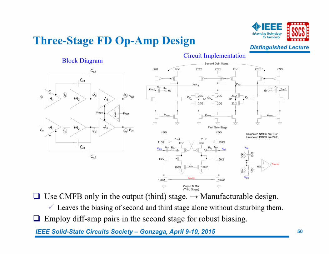
Three-Stage FD Op-Amp Design
VDD VDD
20/2
20/2
20/2
20/2
Vbiasn
vpfbl fbr
vm
VDD
20/2
20/2
VCM
vop1vom1
Unlabeled NMOS are 10/2.Unlabeled PMOS are 22/2.
30K
100f
30K
100f
vom
vop
VCM VCMFB3
VDD VDD
Vbiasn
vop2
VDD VDD
Vbiasn
vom2Cc1
fblR1cCc1
fbrR1c
First Gain Stage
Second Gain Stage
VDD
vomCc2
fblR2c
110/2
100/2
50/2
VCMFB3
VDD
VDD
vopCc2
fbrR2c
110/2
100/2
50/2
VDD
VCM
vop2vom2
Output Buffer(Third Stage)
100/2 100/2
q Use CMFB only in the output (third) stage. → Manufacturable design. ü Leaves the biasing of second and third stage alone without disturbing them.
q Employ diff-amp pairs in the second stage for robust biasing.
-A1 +A2
Cc1
vp vop -A3
Cc2
-+ 1p 2p 3p
-A1 +A2
Cc1
vm vom -A3
Cc2
-+ 1m 2m 3m
CMFB vCMvCMFB
Block Diagram Circuit Implementation
Distinguished Lecture
IEEE Solid-State Circuits Society – Gonzaga, April 9-10, 2015 51
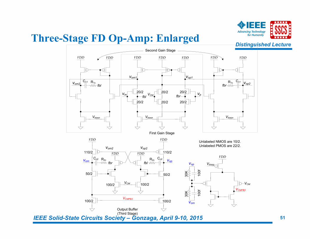
Three-Stage FD Op-Amp: Enlarged VDD VDD
20/2
20/2
20/2
20/2
Vbiasn
vpfbl fbr
vm
VDD
20/2
20/2
VCM
vop1vom1
Unlabeled NMOS are 10/2.Unlabeled PMOS are 22/2.
30K
100f
30K
100f
vom
vop
VCMFB3
VDD VDD
Vbiasn
vop2
VDD VDD
Vbiasn
vom2Cc1
fblR1cCc1
fbrR1c
First Gain Stage
Second Gain Stage
VDD
vomCc2
fblR2c
110/2
100/2
50/2
VCMFB3
VDD
VDD
vopCc2
fbrR2c
110/2
100/2
50/2
VDD
VCM
vop2vom2
Output Buffer(Third Stage)
100/2 100/2
VDD
Vbiasp
VCM
Distinguished Lecture
IEEE Solid-State Circuits Society – Gonzaga, April 9-10, 2015 52
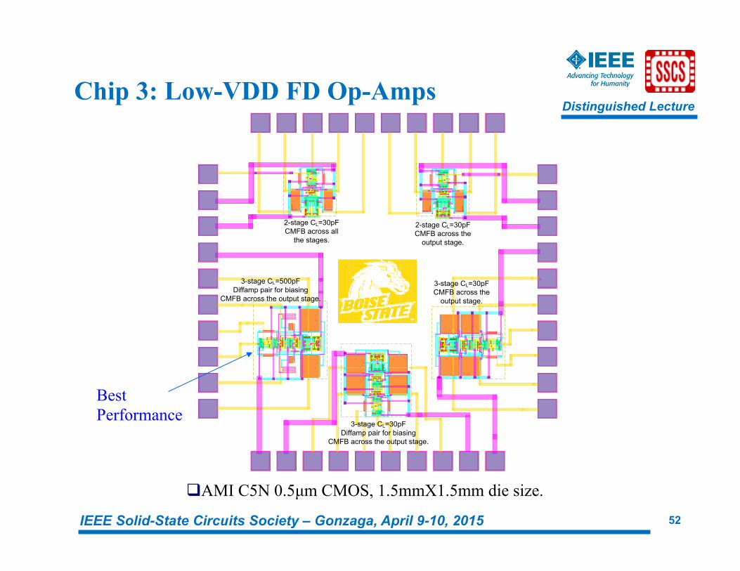
Chip 3: Low-VDD FD Op-Amps
2-stage CL=30pFCMFB across all
the stages.
2-stage CL=30pFCMFB across the
output stage.
3-stage CL=30pFCMFB across the
output stage.
3-stage CL=30pFDiffamp pair for biasing
CMFB across the output stage.
3-stage CL=500pFDiffamp pair for biasing
CMFB across the output stage.
Best Performance
q AMI C5N 0.5µm CMOS, 1.5mmX1.5mm die size.

Distinguished Lecture
IEEE Solid-State Circuits Society – Gonzaga, April 9-10, 2015 53
Simulation and Performance Comparison DC behavior Transient response
82dB gain ts=275ns
q >2.5X figure of merit (FoM).
Distinguished Lecture
IEEE Solid-State Circuits Society – Gonzaga, April 9-10, 2015 54
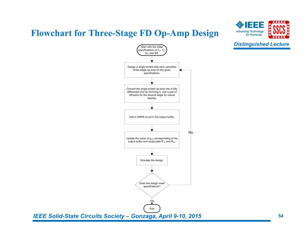
Flowchart for Three-Stage FD Op-Amp Design Start with the initial
specifications on fun, CL, Av, and SR.
Does the design meet specifications?
End
Yes
Design a singly-ended pole-zero cancelled three-stage op-amp for the given
specifications.
Add a CMFB circuit in the output buffer.
Convert the singly-ended op-amp into a fully differential one by mirroring it. Use a pair of
diff-pairs for the second stage for robust biasing.
Simulate the design.
NoUpdate the value of gm3 corresponding to the
output buffer and recalculate R1C and R2C.
Distinguished Lecture
IEEE Solid-State Circuits Society – Gonzaga, April 9-10, 2015 55
Conclusions
q Indirect compensation leads to significantly faster, lower power op-amps with smaller layout area.
q Indirect compensation using split-length devices facilitates low-VDD op-amp design.
q Novel pole-zero canceled three-stage RNIC op-amps exhibit substantial improvement over the state-of-the-art.
q A theory for multi-stage op-amps is presented. q New methodologies for designing multi-stage FD op-amps proposed which
improve the state-of-the-art. q All proposed op-amps are low voltage
ü Open new avenues for low-VDD mixed signal system design.
Distinguished Lecture
IEEE Solid-State Circuits Society – Gonzaga, April 9-10, 2015 56
Future Scope
q Mathematical optimization of PZC op-amps. q Design of low-VDD systems in nano-CMOS process
ü Pipelined and Delta-Sigma data converters, ü Analog filters, ü Audio drivers, etc.
q Further investigation into indirect-compensated op-amps for n≥4 stages.
Distinguished Lecture
IEEE Solid-State Circuits Society – Gonzaga, April 9-10, 2015 57
References
[1] Baker, R.J., “CMOS: Circuit Design, Layout, and Simulation,” 2nd Ed., Wiley Interscience, 2005. [2] Saxena, V., “Indirect Compensation Techniques for Multi-Stage Operational Amplifiers,” M.S. Thesis, ECE
Dept., Boise State University, Oct 2007. [3] The International Technology Roadmap for Semiconductors (ITRS), 2006 [Online]. Available: http://
www.itrs.net/Links/2006Update/2006UpdateFinal.htm [4] Zhao, W., Cao, Yu, "New Generation of Predictive Technology Model for sub-45nm Design
Exploration" [Online]. Available: http://www.eas.asu.edu/~ptm/ [5] Slide courtesy: bwrc.eecs.berkeley.edu/People/Faculty/jan/presentations/ASPDACJanuary05.pdf [6] Leung, K.N., Mok, P.K.T., "Analysis of Multistage Amplifier-Frequency Compensation," IEEE Transactions on
Circuits and Systems I, Fundamental Theory and Applications, vol. 48, no. 9, Sep 2001. [7] You, F., Embabi, S.H.K., Sanchez-Sinencio, E., "Multistage Amplifier Topologies with Nested Gm-C
Compensation," IEEE Journal of Solid State Circuits, vol.32, no.12, Dec 1997. [8] Grasso, A.D., Marano, D., Palumbo, G., Pennisi, S., "Improved Reversed Nested Miller Frequency Compensation
Technique with Voltage Buffer and Resistor," IEEE Transactions on Circuits and Systems-II, Express Briefs, vol.54, no.5, May 2007.
[9] Lee, H., Mok, P.K.T., "Advances in Active-Feedback Frequency Compensation With Power Optimization and Transient Improvement," IEEE Transactions on Circuits and Systems I, Fundamental Theory and Applications, vol.51, no.9, Sep 2004.
[10] Eschauzier, R.G.H., Huijsing, J.H., "A 100-MHz 100-dB operational amplifier with multipath Nested Miller compensation," IEEE Journal of Solid State Circuits, vol. 27, no. 12, pp. 1709-1716, Dec. 1992.
[11] Leung, K. N., Mok, P. K. T., "Nested Miller compensation in low-power CMOS design," IEEE Transaction on Circuits and Systems II, Analog and Digital Signal Processing, vol. 48, no. 4, pp. 388-394, Apr. 2001.
[12] Leung, K. N., Mok, P. K. T., Ki, W. H., Sin, J. K. O., "Three-stage large capacitive load amplifier with damping factor control frequency compensation," IEEE Journal of Solid State Circuits, vol. 35, no. 2, pp. 221-230, Feb. 2000.

Distinguished Lecture
IEEE Solid-State Circuits Society – Gonzaga, April 9-10, 2015 58
References contd.
[13] Peng, X., Sansen, W., "AC boosting compensation scheme for low-power multistage amplifiers," IEEE Journal of Solid State Circuits, vol. 39, no. 11, pp. 2074-2077, Nov. 2004.
[14] Peng, X., Sansen, W., "Transconductances with capacitances feedback compensation for multistage amplifiers," IEEE Journal of Solid State Circuits, vol. 40, no. 7, pp. 1515-1520, July 2005.
[15] Ho, K.-P.,Chan, C.-F., Choy, C.-S., Pun, K.-P., "Reverse nested Miller Compensation with voltage buffer and nulling resistor," IEEE Journal of Solid State Circuits, vol. 38, no. 7, pp. 1735-1738, Oct 2003.
[16] Fan, X., Mishra, C., Sanchez-Sinencio, "Single Miller capacitor frequency compensation technique for low-power multistage amplifiers," IEEE Journal of Solid State Circuits, vol. 40, no. 3, pp. 584-592, March 2005.
[17] Grasso, A.D., Palumbo, G., Pennisi, S., "Advances in Reversed Nested Miller Compensation," IEEE Transactions on Circuits and Systems-I, Regular Papers, vol.54, no.7, July 2007.
[18] Shen, Meng-Hung et al., "A 1.2V Fully Differential Amplifier with Buffered Reverse Nested Miller and Feedforward Compensation," IEEE Asian Solid-State Circuits Conference, 2006, p 171-174.
Distinguished Lecture
IEEE Solid-State Circuits Society – Gonzaga, April 9-10, 2015 59
Questions?


