
BBUV100R011C10
Hardware Description
Issue 04
Date 2016-06-25
HUAWEI TECHNOLOGIES CO., LTD.

Copyright © Huawei Technologies Co., Ltd. 2016. All rights reserved.No part of this document may be reproduced or transmitted in any form or by any means without prior writtenconsent of Huawei Technologies Co., Ltd. Trademarks and Permissions
and other Huawei trademarks are trademarks of Huawei Technologies Co., Ltd.All other trademarks and trade names mentioned in this document are the property of their respectiveholders. NoticeThe purchased products, services and features are stipulated by the contract made between Huawei and thecustomer. All or part of the products, services and features described in this document may not be within thepurchase scope or the usage scope. Unless otherwise specified in the contract, all statements, information,and recommendations in this document are provided "AS IS" without warranties, guarantees orrepresentations of any kind, either express or implied.
The information in this document is subject to change without notice. Every effort has been made in thepreparation of this document to ensure accuracy of the contents, but all statements, information, andrecommendations in this document do not constitute a warranty of any kind, express or implied.
Huawei Technologies Co., Ltd.Address: Huawei Industrial Base
Bantian, LonggangShenzhen 518129People's Republic of China
Website: http://www.huawei.com
Email: [email protected]
Issue 04 (2016-06-25) Huawei Proprietary and ConfidentialCopyright © Huawei Technologies Co., Ltd.
i

About This Document
OverviewA BBU is a baseband unit. This document describes the exteriors and functions of aBBU3900, a BBU3910, and a BBU3910A as well as the configurations, functions, applicationscenarios, and specifications of boards in the BBU3900, BBU3910, and BBU3910A to helpusers comprehensively understand the functions of BBUs. The BBU3910A can be aBBU3910A1, BBU3910A2, or BBU3910A3. A BBU3910A can be used only in a DBS3900(blade site).
The exteriors of components or cables in this document are for reference only. The actualexteriors may be different.
NOTE
Unless otherwise specified, LTE refers to either LTE FDD or LTE TDD, and eNodeB refers to either anLTE FDD eNodeB or an LTE TDD eNodeB in this document. The "L" and "T" in RAT acronyms referto LTE FDD and LTE TDD, respectively.
Product VersionThe following table lists the product versions related to this document.
Product Name Solution Version Product Version
BTS3900 l SRAN11.1l GBSS18.1l RAN18.1l eRAN11.1
V100R011C10
BTS3900A
BTS3900L
BTS3900AL
DBS3900 l SRAN11.1l GBSS18.1l RAN18.1l eRAN11.1l eRAN TDD 11.1
BBUHardware Description About This Document
Issue 04 (2016-06-25) Huawei Proprietary and ConfidentialCopyright © Huawei Technologies Co., Ltd.
ii

Product Name Solution Version Product Version
DBS3900 LampSite l SRAN11.1l RAN18.1l eRAN11.1l eRAN TDD 11.1
BTS3900C l SRAN11.1l RAN18.1
Intended AudienceThis document is intended for:
l Base station installation personnel
l System engineers
l Site maintenance personnel
Organization1 Changes in BBU Hardware Description
This section describes changes in BBU Hardware Description of each version.
2 BBU3900 and BBU3910 Hardware Description
This chapter describes the exteriors, functions, working principles, slot assignment, andboards of a BBU3900 and a BBU3910.
3 BBU3910A Hardware Description
This chapter describes the exterior, working principles, functions, technical specifications,ports, and indicators of a BBU3910A. BBU3910A modules include the following models:BBU3910A1, BBU3910A2, and BBU3910A3. BBU3910A modules of different models havethe same exterior, working principles, functions, ports, and indicators but different technicalspecifications.
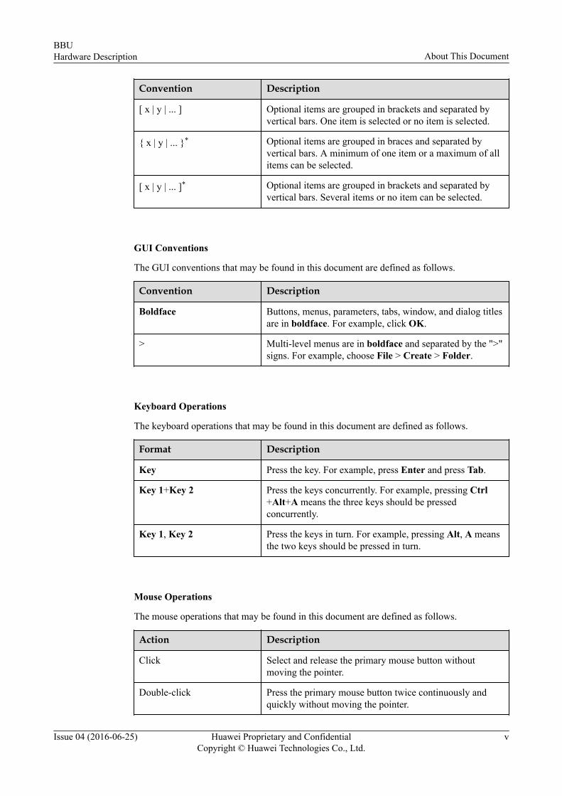
ConventionsSymbol Conventions
The symbols that may be found in this document are defined as follows.
Symbol Description
Indicates an imminently hazardous situation which, if notavoided, will result in death or serious injury.
BBUHardware Description About This Document
Issue 04 (2016-06-25) Huawei Proprietary and ConfidentialCopyright © Huawei Technologies Co., Ltd.
iii

Symbol Description
Indicates a potentially hazardous situation which, if notavoided, could result in death or serious injury.
Indicates a potentially hazardous situation which, if notavoided, may result in minor or moderate injury.
Indicates a potentially hazardous situation which, if notavoided, could result in equipment damage, data loss,performance deterioration, or unanticipated results.NOTICE is used to address practices not related to personalinjury.
Calls attention to important information, best practices andtips.NOTE is used to address information not related topersonal injury, equipment damage, and environmentdeterioration.
General Conventions
The general conventions that may be found in this document are defined as follows.
Convention Description
Times New Roman Normal paragraphs are in Times New Roman.
Boldface Names of files, directories, folders, and users are inboldface. For example, log in as user root.
Italic Book titles are in italics.
Courier New Examples of information displayed on the screen are inCourier New.
Command Conventions
The command conventions that may be found in this document are defined as follows.
Convention Description
Boldface The keywords of a command line are in boldface.
Italic Command arguments are in italics.
[ ] Items (keywords or arguments) in brackets [ ] are optional.
{ x | y | ... } Optional items are grouped in braces and separated byvertical bars. One item is selected.
BBUHardware Description About This Document
Issue 04 (2016-06-25) Huawei Proprietary and ConfidentialCopyright © Huawei Technologies Co., Ltd.
iv
Convention Description
[ x | y | ... ] Optional items are grouped in brackets and separated byvertical bars. One item is selected or no item is selected.
{ x | y | ... }* Optional items are grouped in braces and separated byvertical bars. A minimum of one item or a maximum of allitems can be selected.
[ x | y | ... ]* Optional items are grouped in brackets and separated byvertical bars. Several items or no item can be selected.
GUI Conventions
The GUI conventions that may be found in this document are defined as follows.
Convention Description
Boldface Buttons, menus, parameters, tabs, window, and dialog titlesare in boldface. For example, click OK.
> Multi-level menus are in boldface and separated by the ">"signs. For example, choose File > Create > Folder.
Keyboard Operations
The keyboard operations that may be found in this document are defined as follows.
Format Description
Key Press the key. For example, press Enter and press Tab.
Key 1+Key 2 Press the keys concurrently. For example, pressing Ctrl+Alt+A means the three keys should be pressedconcurrently.
Key 1, Key 2 Press the keys in turn. For example, pressing Alt, A meansthe two keys should be pressed in turn.
Mouse Operations
The mouse operations that may be found in this document are defined as follows.
Action Description
Click Select and release the primary mouse button withoutmoving the pointer.
Double-click Press the primary mouse button twice continuously andquickly without moving the pointer.
BBUHardware Description About This Document
Issue 04 (2016-06-25) Huawei Proprietary and ConfidentialCopyright © Huawei Technologies Co., Ltd.
v
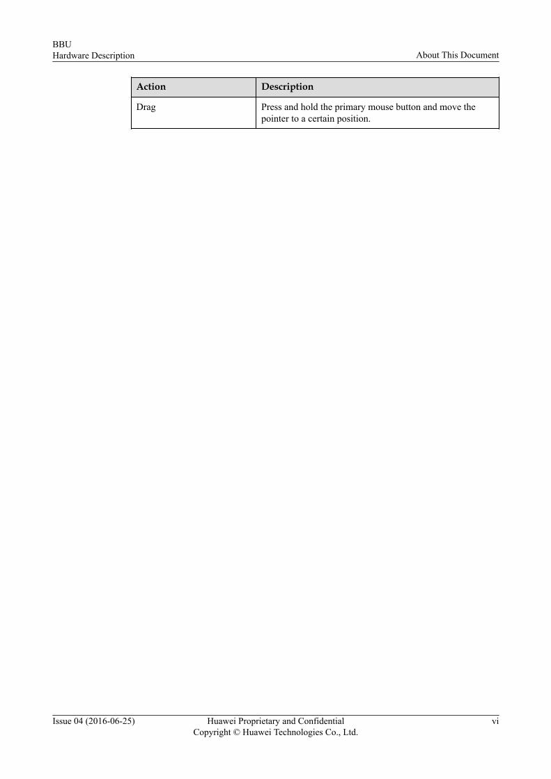
Action Description
Drag Press and hold the primary mouse button and move thepointer to a certain position.
BBUHardware Description About This Document
Issue 04 (2016-06-25) Huawei Proprietary and ConfidentialCopyright © Huawei Technologies Co., Ltd.
vi

Contents
About This Document.....................................................................................................................ii
1 Changes in BBU Hardware Description................................................................................... 1
2 BBU3900 and BBU3910 Hardware Description........................................................................42.1 Exterior of the BBU3900 and BBU3910........................................................................................................................52.2 Working Principles and Functions of a BBU3900 and a BBU3910...............................................................................62.3 Boards and Cabinets or Racks Supported by a BBU3900 and a BBU3910...................................................................82.4 BBU3900 and BBU3910 Slot Assignment.................................................................................................................. 102.4.1 BBU3900 and BBU3910 Slot Distribution............................................................................................................... 102.4.2 BBU3900 Slot Assignment........................................................................................................................................112.4.3 BBU3910 Slot Assignment....................................................................................................................................... 692.5 BBU3900 and BBU3910 Boards................................................................................................................................1072.5.1 UMPT...................................................................................................................................................................... 1072.5.2 WMPT..................................................................................................................................................................... 1142.5.3 GTMU......................................................................................................................................................................1182.5.4 LMPT.......................................................................................................................................................................1252.5.5 LPMP.......................................................................................................................................................................1282.5.6 UBBP.......................................................................................................................................................................1302.5.7 WBBP......................................................................................................................................................................1452.5.8 LBBP....................................................................................................................................................................... 1502.5.9 FAN..........................................................................................................................................................................1602.5.10 UPEU.....................................................................................................................................................................1622.5.11 UEIU......................................................................................................................................................................1662.5.12 UTRP..................................................................................................................................................................... 1672.5.13 USCU.....................................................................................................................................................................1732.5.14 UBRI......................................................................................................................................................................1762.5.15 UCIU..................................................................................................................................................................... 1782.5.16 UCCU.................................................................................................................................................................... 1792.5.17 Optical Modules.................................................................................................................................................... 1802.6 Indicators on BBU Boards..........................................................................................................................................1822.6.1 Status Indicators...................................................................................................................................................... 1822.6.2 Indicators for Ports.................................................................................................................................................. 1852.6.3 Other Indicators....................................................................................................................................................... 192
BBUHardware Description Contents
Issue 04 (2016-06-25) Huawei Proprietary and ConfidentialCopyright © Huawei Technologies Co., Ltd.
vii
2.7 BBU39000&BBU3910 Engineering Specifications.................................................................................................. 193
3 BBU3910A Hardware Description..........................................................................................1973.1 Exterior of a BBU3910A............................................................................................................................................1983.2 Working Principles and Functions of the BBU3910A............................................................................................... 1993.3 BBU3910A Technical Specifications......................................................................................................................... 2003.4 Ports on a BBU3910A................................................................................................................................................ 2143.5 Indicators on a BBU3910A........................................................................................................................................ 216
BBUHardware Description Contents
Issue 04 (2016-06-25) Huawei Proprietary and ConfidentialCopyright © Huawei Technologies Co., Ltd.
viii

1 Changes in BBU Hardware Description
This section describes changes in BBU Hardware Description of each version.
04 (2016-06-25)
This is the fourth commercial release.
Compared with 03 (2016-05-31), this issue does not include or exclude any topics.
Compared with 03 (2016-05-31), this issue includes the following changes.
Topic Change Description
2.6.2 Indicators for Ports Modified the indicator descriptions forFE/GE port.
3.5 Indicators on a BBU3910A Modified the indicator descriptions of GE1.
2.7 BBU39000&BBU3910 EngineeringSpecifications
Modified the heat dissipation capabilities ofBBU3910.
03 (2016-05-31)
This is the third commercial release.
Compared with 02 (2016-04-20), this issue does not include or exclude any topics.
Compared with 02 (2016-04-20), this issue includes the following changes.
Topic Change Description
l 2.3 Boards and Cabinets or RacksSupported by a BBU3900 and aBBU3910
l 2.5.1 UMPTl 2.5.6 UBBPl 2.6.2 Indicators for Ports
Added the description of the UMPTe andUBBPe.
BBUHardware Description 1 Changes in BBU Hardware Description
Issue 04 (2016-06-25) Huawei Proprietary and ConfidentialCopyright © Huawei Technologies Co., Ltd.
1

02 (2016-04-20)This is the second commercial release.
Compared with 01 (2016-03-07), this issue does not include or exclude any topics.
Compared with 01 (2016-03-07), this issue includes the following changes.
Topic Change Description
l 2.5.1 UMPTl 2.5.6 UBBPl 2.5.7 WBBPl 2.5.8 LBBP
Added a note of the capacity license.
2.5.10 UPEU Added the configuration compliance ofFANc and UPEUc.
01 (2016-03-07)This is the first commercial release.
Compared with Draft A (2015-12-30), this issue does not include any changes.
Draft A (2015-12-30)This is a draft.
Compared with Issue 03 (2015-08-30) of V100R010C10, this issue includes the followingnew topics:l 2.6 Indicators on BBU Boards and its child topics
Compared with Issue 03 (2015-08-30) of V100R010C10, this issue includes the followingchanges.
Topic Change Description
Child topics of 2.5 BBU3900 andBBU3910 Boards
Removed indicator descriptions.
2.5.1 UMPT Added the description that the FE/GE0 andFE/GE1 ports can be used at the same time.
l BBU Slot Assignment in GSM BaseStations
l BBU Slot Assignment in GSM BaseStations
l 2.5.3 GTMU
Added the description that the GTMUcsupports SingleOM.
BBUHardware Description 1 Changes in BBU Hardware Description
Issue 04 (2016-06-25) Huawei Proprietary and ConfidentialCopyright © Huawei Technologies Co., Ltd.
2

Topic Change Description
l 2.3 Boards and Cabinets or RacksSupported by a BBU3900 and aBBU3910
l 2.5.3 GTMU
Added the information of the GTMUc.
l BBU3900 slot assignment– BBU Slot Assignment in GSM Base
Stations– BBU Slot Assignment in GU and
G*U Base Stations– BBU Slot Assignment in GL and
G*L Base Stations– BBU Slot Assignment in Triple-
Mode Base Stationsl BBU3910 slot assignment
– BBU Slot Assignment in GSM BaseStations
– BBU Slot Assignment in GU andG*U Base Stations
– BBU Slot Assignment in GL andG*L Base Stations
Added the description that the GTMUc issupported in a GSM, a GU, a GL, and aseparate-MPT triple-mode base station.
2.5.17 Optical Modules l Added the description of the single-fiberbidirectional optical module.
l Added the certificate standards andrequirements of optical modules.
Compared with Issue 03 (2015-08-30) of V100R010C10, this issue does not exclude anytopics.
BBUHardware Description 1 Changes in BBU Hardware Description
Issue 04 (2016-06-25) Huawei Proprietary and ConfidentialCopyright © Huawei Technologies Co., Ltd.
3
2 BBU3900 and BBU3910 Hardware
Description
About This Chapter
This chapter describes the exteriors, functions, working principles, slot assignment, andboards of a BBU3900 and a BBU3910.
Unless otherwise specified, the BBU refers to both the BBU3900 and BBU3910 in thischapter.
2.1 Exterior of the BBU3900 and BBU3910A BBU, which has a case structure, is 19 inches wide and 2 U high.
2.2 Working Principles and Functions of a BBU3900 and a BBU3910A BBU is a baseband unit. It processes baseband signals of a base station.
2.3 Boards and Cabinets or Racks Supported by a BBU3900 and a BBU3910This section describes boards and cabinets or racks supported by different types of BBUs.
2.4 BBU3900 and BBU3910 Slot AssignmentThis chapter describes BBU slot distribution, BBU3910 slot assignment, and BBU3900 slotassignment.
2.5 BBU3900 and BBU3910 BoardsA BBU includes the following boards: main processing board, baseband processing board,transmission extension board, fan module, power module, monitoring module, clock boardwith a satellite card, baseband extension board, and infrastructure interconnection board.
2.6 Indicators on BBU BoardsThis chapter describes the indicators on BBU boards.
2.7 BBU39000&BBU3910 Engineering SpecificationsBBU equipment specifications include the input power specifications, dimensions, weight,heat dissipation capabilities, environmental specifications, and surge protection specifications.
BBUHardware Description 2 BBU3900 and BBU3910 Hardware Description
Issue 04 (2016-06-25) Huawei Proprietary and ConfidentialCopyright © Huawei Technologies Co., Ltd.
4
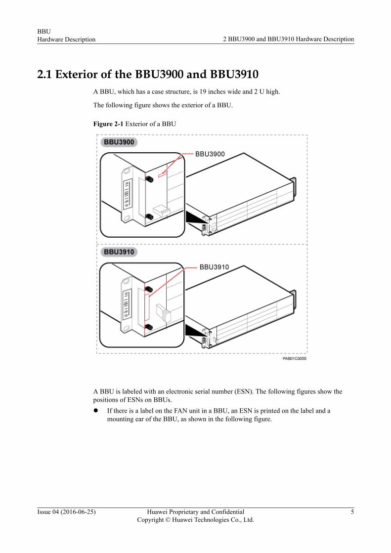
2.1 Exterior of the BBU3900 and BBU3910A BBU, which has a case structure, is 19 inches wide and 2 U high.
The following figure shows the exterior of a BBU.
Figure 2-1 Exterior of a BBU
A BBU is labeled with an electronic serial number (ESN). The following figures show thepositions of ESNs on BBUs.l If there is a label on the FAN unit in a BBU, an ESN is printed on the label and a
mounting ear of the BBU, as shown in the following figure.
BBUHardware Description 2 BBU3900 and BBU3910 Hardware Description
Issue 04 (2016-06-25) Huawei Proprietary and ConfidentialCopyright © Huawei Technologies Co., Ltd.
5

Figure 2-2 ESN position 1
l If there is no label on the FAN unit in a BBU, an ESN is printed on a mounting ear of the
BBU, as shown in the following figure.
Figure 2-3 ESN position 2
NOTEAn ESN is a unique identifier of a device and is used during base station commissioning.
2.2 Working Principles and Functions of a BBU3900 and aBBU3910
A BBU is a baseband unit. It processes baseband signals of a base station.
Working PrincipleA BBU consists of the following subsystems: baseband subsystem, power and mechanicalsubsystem, transmission subsystem, interconnection subsystem, main control subsystem,monitoring subsystem, and clock subsystem. Each subsystem consists of different modules.l The baseband subsystem consists of the baseband processing unit.l The power and mechanical subsystem consists of the backplane, fan, and power module.l The transmission subsystem consists of the main control and transmission unit as well as
the transmission extension unit.
BBUHardware Description 2 BBU3900 and BBU3910 Hardware Description
Issue 04 (2016-06-25) Huawei Proprietary and ConfidentialCopyright © Huawei Technologies Co., Ltd.
6
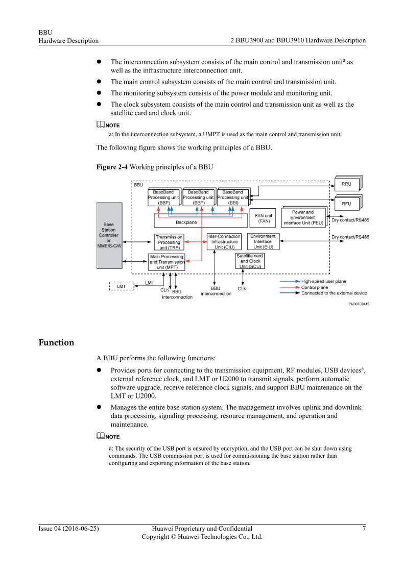
l The interconnection subsystem consists of the main control and transmission unita aswell as the infrastructure interconnection unit.
l The main control subsystem consists of the main control and transmission unit.l The monitoring subsystem consists of the power module and monitoring unit.l The clock subsystem consists of the main control and transmission unit as well as the
satellite card and clock unit.
NOTEa: In the interconnection subsystem, a UMPT is used as the main control and transmission unit.
The following figure shows the working principles of a BBU.
Figure 2-4 Working principles of a BBU
FunctionA BBU performs the following functions:
l Provides ports for connecting to the transmission equipment, RF modules, USB devicesa,external reference clock, and LMT or U2000 to transmit signals, perform automaticsoftware upgrade, receive reference clock signals, and support BBU maintenance on theLMT or U2000.
l Manages the entire base station system. The management involves uplink and downlinkdata processing, signaling processing, resource management, and operation andmaintenance.
NOTE
a: The security of the USB port is ensured by encryption, and the USB port can be shut down usingcommands. The USB commission port is used for commissioning the base station rather thanconfiguring and exporting information of the base station.
BBUHardware Description 2 BBU3900 and BBU3910 Hardware Description
Issue 04 (2016-06-25) Huawei Proprietary and ConfidentialCopyright © Huawei Technologies Co., Ltd.
7
2.3 Boards and Cabinets or Racks Supported by a BBU3900and a BBU3910
This section describes boards and cabinets or racks supported by different types of BBUs.
Boards Supported by BBUs
The following table describes boards supported by different types of BBUs, regardless ofmode and configuration.
Table 2-1 Boards supported by BBUs
Board Type Board Supported by a BBU3900 Board Supported by a BBU3910
Main controlboard
l GTMU, GTMUb, or GTMUcl WMPTl LMPTl UMPTa (UMPTa1, UMPTa2, or
UMPTa6)l UMPTb (UMPTb1 or UMPTb2)l UMPTe (UMPTe1 or UMPTe2)
l GTMUb or GTMUcl UMPTb (UMPTb1 or UMPTb2)l UMPTe (UMPTe1 or UMPTe2)
Basebandprocessingboard
l UBBPd (UBBPd1 to UBBPd6,UBBPda, or UBBPd9)
l UBBPe (UBBPe1 to UBBPe6,or UBBPe9)
l WBBP (WBBPa, WBBPb1 toWBBPb4, WBBPd1 toWBBPd3, or WBBPf1 toWBBPf4)
l LBBP (LBBPc, or LBBPd1 toLBBPd4)
l UBBPd (UBBPd1 to UBBPd6,UBBPda, or UBBPd9)
l UBBPe (UBBPe1 to UBBPe6,or UBBPe9)
Transmissionextensionboard
UTRP (UTRP2 to UTRP4, UTRP6,UTRP9, UTRPa, UTRPb4, orUTRPc)
UTRPa or UTRPc
Basebandradiointerfaceboard
UBRI or UBRIb UBRIb
Satellite-cardboard
USCUb22, USCUb14, or USCUb11 USCUb14 or USCUb11
Fan module FAN or FANc FANd or FANe
Powermodule
UPEUa, UPEUb, or UPEUc UPEUd
BBUHardware Description 2 BBU3900 and BBU3910 Hardware Description
Issue 04 (2016-06-25) Huawei Proprietary and ConfidentialCopyright © Huawei Technologies Co., Ltd.
8

Board Type Board Supported by a BBU3900 Board Supported by a BBU3910
Environmentmonitoringunit
UEIU UEIU
Interconnection board
l UCIUl UCCU
UCCU
Cabinets or Racks Supported by BBUs
The following table describes the cabinets or racks supported by different types of BBUs.
Table 2-2 Cabinets or racks supported by BBUs
BaseStationType
Cabinet or Rack Supported by aBBU3900
Cabinet or Rack Supported by aBBU3910
BTS3900 BTS3900 (Ver.B), BTS3900 (Ver.C),BTS3900 (Ver.D), BTS3900(Ver.D_A), or BTS3900 (Ver.D_B)cabinet
BTS3900 (Ver.D), BTS3900(Ver.D_A), or BTS3900 (Ver.D_B)cabinet
BTS3900L BTS3900L (Ver.B), BTS3900L(Ver.C), BTS3900L (Ver.D), orBTS3900L (Ver.D_B) cabinet
BTS3900L (Ver.D) or BTS3900L(Ver.D_B) cabinet
BTS3900A l APM30H (Ver.B), APM30H(Ver.C), APM30H (Ver.D),APM30H (Ver.E), APM30H(Ver.D_C), APM30H (Ver.D_B),APM30H (Ver.D_A2), APM30(Ver.D_A1), APM30H(Ver.E_B~D), APM30H(Ver.E_A2), or APM30(Ver.E_A1)
l TMC11H (Ver.B), TMC11H(Ver.C), TMC11H (Ver.D),TMC11H (Ver.E), TMC11H(Ver.D_C), TMC11H (Ver.D_B),TMC11H (Ver.D_A2), TMC(Ver.D_A1), TMC11H(Ver.E_B~D), TMC11H(Ver.E_A2), or TMC (Ver.E_A1)
l APM30H (Ver.D), APM30H,(Ver.E), APM30H (Ver.D_C),APM30H (Ver.D_B), APM30H(Ver.D_A2), APM30(Ver.D_A1), APM30H(Ver.E_B~D), APM30H(Ver.E_A2), or APM30(Ver.E_A1)
l TMC11H (Ver.D), TMC11H(Ver.E), TMC11H (Ver.D_C),TMC11H (Ver.D_B), TMC11H(Ver.D_A2), TMC (Ver.D_A1),TMC11H (Ver.E_B~D),TMC11H (Ver.E_A2), or TMC(Ver.E_A1)
BTS3900AL
BTS3900AL (Ver.A) cabinet BTS3900AL (Ver.A) cabinet
BTS3012(Ver.D_Z)
BTS3012 (Ver.D_Z) cabinet BTS3012 (Ver.D_Z) cabinet
BBUHardware Description 2 BBU3900 and BBU3910 Hardware Description
Issue 04 (2016-06-25) Huawei Proprietary and ConfidentialCopyright © Huawei Technologies Co., Ltd.
9

BaseStationType
Cabinet or Rack Supported by aBBU3900
Cabinet or Rack Supported by aBBU3910
BTS3012AE(Ver.D_Z)
BTS3012AE (Ver.D_Z) cabinet BTS3012AE (Ver.D_Z) cabinet
DBS3900 l APM30H (Ver.B), APM30H(Ver.C), APM30H (Ver.D),APM30H (Ver.E), APM30H(Ver.D_C), APM30H (Ver.D_B),APM30H (Ver.D_A2), APM30(Ver.D_A1), APM30H(Ver.E_B~D), APM30H(Ver.E_A2), or APM30(Ver.E_A1)
l TMC11H (Ver.B), TMC11H(Ver.C), TMC11H (Ver.D),TMC11H (Ver.E), TMC11H(Ver.D_C), TMC11H (Ver.D_B),TMC11H (Ver.D_A2), TMC(Ver.D_A1), TMC11H(Ver.E_B~D), TMC11H(Ver.E_A2), or TMC (Ver.E_A1)
l OMB, OMB (Ver.C), IMB03,INS12, TP48600A, or IBC10
l APM30H (Ver.D), APM30H,(Ver.E), APM30H (Ver.D_C),APM30H (Ver.D_B), APM30H(Ver.D_A2), APM30(Ver.D_A1), APM30H(Ver.E_B~D), APM30H(Ver.E_A2), or APM30(Ver.E_A1)
l TMC11H (Ver.D), TMC11H(Ver.E), TMC11H (Ver.D_C),TMC11H (Ver.D_B), TMC11H(Ver.D_A2), TMC (Ver.D_A1),TMC11H (Ver.E_B~D),TMC11H (Ver.E_A2), or TMC(Ver.E_A1)
l OMB (Ver.C) or IMB03
BTS3900C OMB or OMB (Ver.C) OMB (Ver.C)
2.4 BBU3900 and BBU3910 Slot AssignmentThis chapter describes BBU slot distribution, BBU3910 slot assignment, and BBU3900 slotassignment.
2.4.1 BBU3900 and BBU3910 Slot DistributionThis section describes BBU slot distribution.
A BBU has 11 slots. The following figure shows BBU slot distribution.
Figure 2-5 BBU slot distribution
BBUHardware Description 2 BBU3900 and BBU3910 Hardware Description
Issue 04 (2016-06-25) Huawei Proprietary and ConfidentialCopyright © Huawei Technologies Co., Ltd.
10

In all scenarios, a FAN, a UPEU, and a UEIU are configured in fixed slots in a BBU. Thefollowing table describes the principles for configuring a FAN, a UPEU, and a UEIU.
Table 2-3 Principles for configuring a FAN, a UPEU, and a UEIU
BoardType
BoardName
Mandatory MaximumQuantity
Slot AssignmentSequence (the LeftmostSlot Has the HighestPriority)
Fan unit FAN Yes 1 Slot 16 -
Power andenvironmentinterfaceunit
UPEU Yes 2 Slot 19 Slot 18
Environmentmonitoringunit
UEIU No 1 Slot 18 -
2.4.2 BBU3900 Slot AssignmentThis section describes the principles for BBU3900 slot assignment.
BBU Slot Assignment in GSM Base Stations
This section describes the principles for BBU3900 slot assignment in GSM base stations.
GBTS
The following figure shows the BBU slot assignment in a GBTS.
Figure 2-6 BBU slot assignment
The following table describes the principles for BBU slot assignment.
BBUHardware Description 2 BBU3900 and BBU3910 Hardware Description
Issue 04 (2016-06-25) Huawei Proprietary and ConfidentialCopyright © Huawei Technologies Co., Ltd.
11

Table 2-4 Principles for BBU slot assignment
Priority
BoardType
BoardName
Mandatory
MaximumQuantity
Slot Assignment Sequence (theLeftmost Slot Has the Highest Priority)
1 Maincontrolboard
l GTMU
l GTMUb
l GTMUc
Yes 1 Slot 6 - - - -
2 Interconnectionboard
UCIU No 1 Slot 4 Slot 0 Slot 1 - -
3 Transmissionboard
UTRPb4
No 1 Slot 4 Slot 0 - - -
4 Satellite-cardboard
USCUb22
No 1 Slot 1 - - - -
USCUb14
No 1 Slot 4 Slot 1 Slot 0 - -
5 Basebandradiointerfaceboard
l UBRIb
l UBRI
No 1 Slot 2 - - - -
6 Basebandprocessingboard
UBBP_G
No 2 Slot 1 Slot 2 Slot 0 Slot 4 Slot 3
NOTE
l If two or more baseband boards in GSM mode are required, ensure that at least one of the basebandboard (UBBPd_G or UBRIb) is installed in slot 1, slot 2, or slot 3.
l In a GBTS, the UBBP_G installed in slot 4 cannot be connected to CPRI cables.
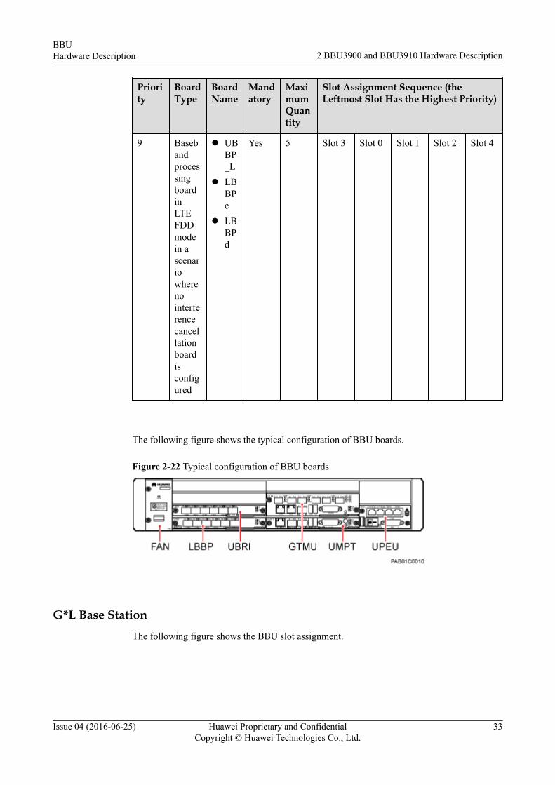
The following figure shows the typical configuration of BBU boards.
BBUHardware Description 2 BBU3900 and BBU3910 Hardware Description
Issue 04 (2016-06-25) Huawei Proprietary and ConfidentialCopyright © Huawei Technologies Co., Ltd.
12

Figure 2-7 Typical configuration of BBU boards
eGBTSThe following figure shows the BBU slot assignment in an eGBTS.
Figure 2-8 BBU slot assignment (1)
Figure 2-9 BBU slot assignment (2)
The following table describes the principles for BBU slot assignment.
BBUHardware Description 2 BBU3900 and BBU3910 Hardware Description
Issue 04 (2016-06-25) Huawei Proprietary and ConfidentialCopyright © Huawei Technologies Co., Ltd.
13
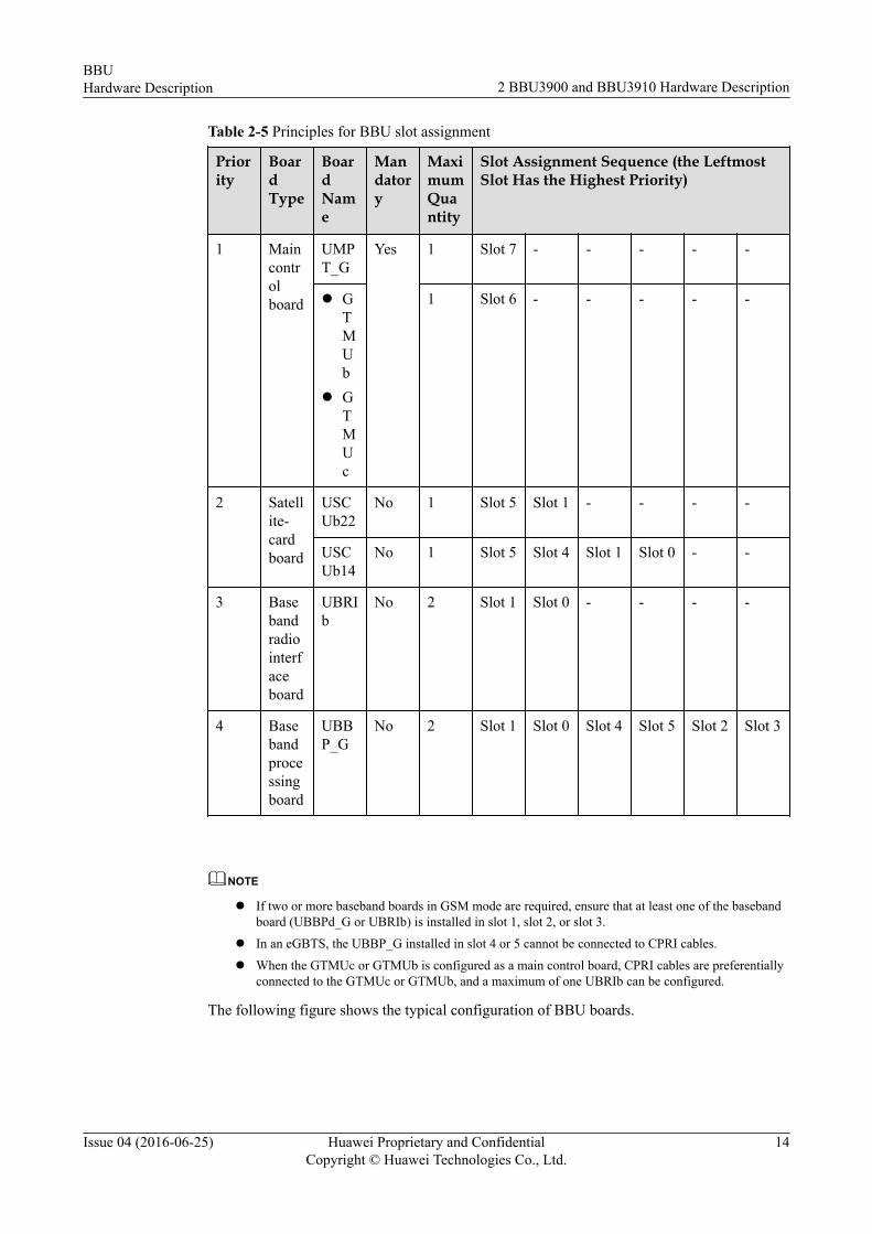
Table 2-5 Principles for BBU slot assignment
Priority
BoardType
BoardName
Mandatory
MaximumQuantity
Slot Assignment Sequence (the LeftmostSlot Has the Highest Priority)
1 Maincontrolboard
UMPT_G
Yes 1 Slot 7 - - - - -
l GTMUb
l GTMUc
1 Slot 6 - - - - -
2 Satellite-cardboard
USCUb22
No 1 Slot 5 Slot 1 - - - -
USCUb14
No 1 Slot 5 Slot 4 Slot 1 Slot 0 - -
3 Basebandradiointerfaceboard
UBRIb
No 2 Slot 1 Slot 0 - - - -
4 Basebandprocessingboard
UBBP_G
No 2 Slot 1 Slot 0 Slot 4 Slot 5 Slot 2 Slot 3
NOTE
l If two or more baseband boards in GSM mode are required, ensure that at least one of the basebandboard (UBBPd_G or UBRIb) is installed in slot 1, slot 2, or slot 3.
l In an eGBTS, the UBBP_G installed in slot 4 or 5 cannot be connected to CPRI cables.
l When the GTMUc or GTMUb is configured as a main control board, CPRI cables are preferentiallyconnected to the GTMUc or GTMUb, and a maximum of one UBRIb can be configured.
The following figure shows the typical configuration of BBU boards.
BBUHardware Description 2 BBU3900 and BBU3910 Hardware Description
Issue 04 (2016-06-25) Huawei Proprietary and ConfidentialCopyright © Huawei Technologies Co., Ltd.
14

Figure 2-10 Typical configuration of BBU boards
BBU Slot Assignment in UMTS Base StationsThis section describes the principles for BBU3900 slot assignment in UMTS base stations.
NOTE
l In a UMTS base station, the UMPT and WMPT cannot be configured in the same BBU.
l The baseband processing board in UMTS mode configured only in slot 3 or 2 can be connected to CPRIcables. The UBBP_U, WBBPd, or WBBPf is preferentially configured in slot 3 or 2. The configurationpriority of these types of boards is UBBP_U > WBBPf > WBBPd.
l If five or more baseband processing boards work in UMTS mode, ensure that a UBBP_U, WBBPd, orWBBPf is configured in slot 3.
l If slots 2 and 3 are occupied by WBBPa or WBBPb boards, exchange boards to ensure that a UBBP_U,WBBPd, or WBBPf is configured in slot 3 or 2. A UBBP_U, WBBPd, or WBBPf is preferentiallyconfigured in slot 3.
Single BBU ScenarioThe following figure shows the BBU slot assignment in a UMTS base station.
Figure 2-11 BBU slot assignment
The following table describes the principles for BBU slot assignment in a UMTS base station.
BBUHardware Description 2 BBU3900 and BBU3910 Hardware Description
Issue 04 (2016-06-25) Huawei Proprietary and ConfidentialCopyright © Huawei Technologies Co., Ltd.
15
Table 2-6 Principles for BBU slot assignment
Priority
BoardType
BoardName
Mandatory
MaximumQuantity
Slot Assignment Sequence (the LeftmostSlot Has the Highest Priority)
1 Maincontrolboard
l UMPT_U
l WMPT
Yes 2 Slot 7 Slot 6 - - - -
2 Transmissionboard
UTRPc
No 1 Slot 4 Slot 5 Slot 0 Slot 1 - -
l UTRP6
l UTRP9
l UTRP2
l UTRPa
l UTRP3
l UTRP4
No 2 Slot 4 Slot 5 Slot 0 Slot 1 - -
BBUHardware Description 2 BBU3900 and BBU3910 Hardware Description
Issue 04 (2016-06-25) Huawei Proprietary and ConfidentialCopyright © Huawei Technologies Co., Ltd.
16

Priority
BoardType
BoardName
Mandatory
MaximumQuantity
Slot Assignment Sequence (the LeftmostSlot Has the Highest Priority)
3 Satellite-cardboard
USCUb22
No 1 Slot 5 Slot 1 - - - -
USCUb14
No 1 Slot 5 Slot 4 Slot 1 Slot 0 - -
4 BasebandprocessingboardnotprovidingadditionalCPRIports
l UBBP_U
l WBBPf
l WBBPd
l WBBPb
l WBBPa
Yes 6 Slot 3 Slot 0 Slot 1 Slot 2 Slot 4 Slot 5
BBUHardware Description 2 BBU3900 and BBU3910 Hardware Description
Issue 04 (2016-06-25) Huawei Proprietary and ConfidentialCopyright © Huawei Technologies Co., Ltd.
17

Priority
BoardType
BoardName
Mandatory
MaximumQuantity
Slot Assignment Sequence (the LeftmostSlot Has the Highest Priority)
BasebandprocessingboardprovidingadditionalCPRIports
l UBBP_U
l WBBPf
l WBBPd
l WBBPb
l WBBPa
Yes 6 Slot 3 Slot 2 Slot 0 Slot 1 Slot 4 Slot 5
The following figure shows the typical configuration of BBU boards.
Figure 2-12 Typical configuration of BBU boards
BBU Interconnection Scenario
In a scenario where two or more BBUs are connected to universal switching units (USUs)using interconnection signal cables, the principles for BBU slot assignment are different from
BBUHardware Description 2 BBU3900 and BBU3910 Hardware Description
Issue 04 (2016-06-25) Huawei Proprietary and ConfidentialCopyright © Huawei Technologies Co., Ltd.
18
those in a single BBU scenario. The following figure shows the principles for BBU slotassignment in a BBU interconnection scenario.
Figure 2-13 BBU slot assignment
The following table describes the principles for BBU slot assignment in a BBUinterconnection scenario.
Table 2-7 Principles for BBU slot assignment
Priority
BoardType
BoardName
Mandatory
MaximumQuantity
Slot Assignment Sequence (the LeftmostSlot Has the Highest Priority)
1 Maincontrolboard
UMPT_U
Yes 2 Slot 7 Slot 6 - - - -
2 Interconnectionboard
UCCU
Yes 1 Slot 3 Slot 2 Slot 4 Slot 5 Slot 0 Slot 1
3 Basebandprocessingboard
l UBBP_U
l WBBPd
l WBBPf
Yes 6 Slot 3 Slot 2 Slot 4 Slot 5 Slot 0 Slot 1
BBUHardware Description 2 BBU3900 and BBU3910 Hardware Description
Issue 04 (2016-06-25) Huawei Proprietary and ConfidentialCopyright © Huawei Technologies Co., Ltd.
19
BBU Slot Assignment in LTE FDD/LTE TDD Base Stations
This section describes the principles for BBU3900 slot assignment in LTE FDD and LTETDD base stations.
NOTE
l In an LTE FDD or LTE TDD base station, and the UMPT and LMPT are installed in the same BBU,only one board can be used as the main control board.
l An LPMP can be used only in an LTE FDD base station and cannot be used in an LTE TDD basestation.
Single BBU Scenario
The principles for BBU slot assignment in an LTE FDD base station are the same as those inan LTE TDD base station. This section uses the BBU slot assignment in an LTE FDD basestation as an example. The following figure shows the BBU slot assignment.
Figure 2-14 BBU slot assignment
The following table describes the principles for BBU slot assignment.
Table 2-8 Principles for BBU slot assignment
Priority
BoardType
BoardName
Mandatory
MaximumQuantity
Slot Assignment Sequence (the LeftmostSlot Has the Highest Priority)
1 MaincontrolboardinLTEFDDmode
l UMPT_L
l LMPT
Yes 2 Slot 7 Slot 6 - - - -
BBUHardware Description 2 BBU3900 and BBU3910 Hardware Description
Issue 04 (2016-06-25) Huawei Proprietary and ConfidentialCopyright © Huawei Technologies Co., Ltd.
20
Priority
BoardType
BoardName
Mandatory
MaximumQuantity
Slot Assignment Sequence (the LeftmostSlot Has the Highest Priority)
2 Satellite-cardboard
USCUb22
No 1 Slot 5 Slot 1 - - - -
l USCUb14
l USCUb11
No 1 Slot 5 Slot 4 Slot 1 Slot 0 - -
3 InterferencecancellationboardinLTEmode
LPMP
No 1 Slot 2 - - - - -
4 BasebandprocessingboardinLTEFDDmode
l UBBP_L
l LBBPd
l LBBPc
Yes 6 Slot 3 Slot 0 Slot 1 Slot 2 Slot 4 Slot 5
The following figure shows the typical configuration of BBU boards.
BBUHardware Description 2 BBU3900 and BBU3910 Hardware Description
Issue 04 (2016-06-25) Huawei Proprietary and ConfidentialCopyright © Huawei Technologies Co., Ltd.
21
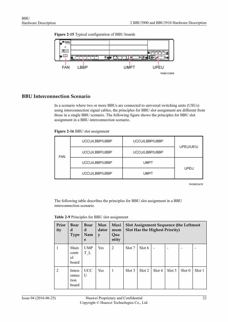
Figure 2-15 Typical configuration of BBU boards
BBU Interconnection Scenario
In a scenario where two or more BBUs are connected to universal switching units (USUs)using interconnection signal cables, the principles for BBU slot assignment are different fromthose in a single BBU scenario. The following figure shows the principles for BBU slotassignment in a BBU interconnection scenario.
Figure 2-16 BBU slot assignment
The following table describes the principles for BBU slot assignment in a BBUinterconnection scenario.
Table 2-9 Principles for BBU slot assignment
Priority
BoardType
BoardName
Mandatory
MaximumQuantity
Slot Assignment Sequence (the LeftmostSlot Has the Highest Priority)
1 Maincontrolboard
UMPT_L
Yes 2 Slot 7 Slot 6 - - - -
2 Interconnectionboard
UCCU
Yes 1 Slot 3 Slot 2 Slot 4 Slot 5 Slot 0 Slot 1
BBUHardware Description 2 BBU3900 and BBU3910 Hardware Description
Issue 04 (2016-06-25) Huawei Proprietary and ConfidentialCopyright © Huawei Technologies Co., Ltd.
22

Priority
BoardType
BoardName
Mandatory
MaximumQuantity
Slot Assignment Sequence (the LeftmostSlot Has the Highest Priority)
3 Basebandprocessingboard
l UBBP_L
l LBBPd_L
Yes 6 Slot 3 Slot 2 Slot 4 Slot 5 Slot 0 Slot 1
BBU Slot Assignment in GU and G*U Base StationsThis section describes the principles for BBU3900 slot assignment in GU and G*U basestations.
NOTE
l The GU base station is a separate-MPT GSM and UMTS dual-mode base station. In a GU basestation, one BBU is configured with two main control boards, of which one works in GSM modeand the other works in UMTS mode.
l The G*U base station is a co-MPT GSM and UMTS dual-mode base station. In a G*U base station,one main control board in a BBU can work in GSM and UMTS dual-mode.
NOTE
l The baseband processing board in UMTS mode configured only in slot 3 or 2 can be connected toCPRI cables. The UBBP_U, WBBPd, or WBBPf is preferentially configured in slot 3 or 2. Theconfiguration priority of these types of boards is UBBP_U > WBBPf > WBBPd.
l If five or more baseband processing boards work in UMTS mode, ensure that a UBBP_U, WBBPd,or WBBPf is configured in slot 3.
l If slots 2 and 3 are occupied by WBBPa or WBBPb boards, exchange boards to ensure that aUBBP_U, WBBPd, or WBBPf is configured in slot 3 or 2. A UBBP_U, WBBPd, or WBBPf ispreferentially configured in slot 3.
l If two or more baseband boards in GSM mode are required, ensure that at least one of the basebandboard (UBBPd_G or UBRIb) is installed in slot 1, slot 2, or slot 3.
l In a GBTS, the UBBP_G installed in slot 4 cannot be connected to CPRI cables.
GU Base StationThe following figure shows the BBU slot assignment in a GU base station.
BBUHardware Description 2 BBU3900 and BBU3910 Hardware Description
Issue 04 (2016-06-25) Huawei Proprietary and ConfidentialCopyright © Huawei Technologies Co., Ltd.
23

Figure 2-17 BBU slot assignment
The following table describes the principles for BBU slot assignment.
Table 2-10 Principles for BBU slot assignment
Priority
BoardType
BoardName
Mandatory
MaximumQuantity
Slot Assignment Sequence (theLeftmost Slot Has the Highest Priority)
1 MaincontrolboardinGSMmode
l GTMU
l GTMUb
l GTMUc
Yes 1 Slot 6 - - - -
2 MaincontrolboardinUMTSmode
l UMPT_U
l WMPT
Yes 1 Slot 7 - - - -
3 TransmissionboardinGSMmode
UTRPb4
No 1 Slot 4 Slot 0 - - -
BBUHardware Description 2 BBU3900 and BBU3910 Hardware Description
Issue 04 (2016-06-25) Huawei Proprietary and ConfidentialCopyright © Huawei Technologies Co., Ltd.
24

Priority
BoardType
BoardName
Mandatory
MaximumQuantity
Slot Assignment Sequence (theLeftmost Slot Has the Highest Priority)
4 TransmissionboardinUMTSmode
UTRPc
No 1 Slot 4 Slot 0 Slot 1 - -
l UTRP6
l UTRP9
l UTRP2
l UTRPa
l UTRP3
l UTRP4
No 2 Slot 4 Slot 0 Slot 1 - -
5 Satellite-cardboard
USCUb22
No 1 Slot 1 - - - -
USCUb14
No 1 Slot 4 Slot 1 Slot 0 - -
6 BasebandradiointerfaceboardinGSMmode
l UBRIb
l UBRI
No 1 Slot 2 - - - -
7 BasebandprocessingboardinGSMmode
UBBP_G
No 2 Slot 1 Slot 2 Slot 0 Slot 4 -
BBUHardware Description 2 BBU3900 and BBU3910 Hardware Description
Issue 04 (2016-06-25) Huawei Proprietary and ConfidentialCopyright © Huawei Technologies Co., Ltd.
25
Priority
BoardType
BoardName
Mandatory
MaximumQuantity
Slot Assignment Sequence (theLeftmost Slot Has the Highest Priority)
8 BasebandprocessingboardinUMTSmodenotprovidingadditionalCPRIports
l UBBP_U
l WBBPf
l WBBPd
l WBBPb
l WBBPa
Yes 5 Slot 3 Slot 0 Slot 1 Slot 2 Slot 4
BasebandprocessingboardinUMTSmodeprovidingadditionalCPRIports
l UBBP_U
l WBBPf
l WBBPd
l WBBPb
l WBBPa
Yes 5 Slot 3 Slot 2 Slot 0 Slot 1 Slot 4
The following figure shows the typical configuration of BBU boards.
Figure 2-18 Typical configuration of BBU boards
BBUHardware Description 2 BBU3900 and BBU3910 Hardware Description
Issue 04 (2016-06-25) Huawei Proprietary and ConfidentialCopyright © Huawei Technologies Co., Ltd.
26

G*U Base StationThe following figure shows the BBU slot assignment in a G*U base station.
Figure 2-19 BBU slot assignment
The following table describes the principles for BBU slot assignment.
Table 2-11 Principles for BBU slot assignment
Priority
BoardType
BoardName
Mandatory
MaximumQuantity
Slot Assignment Sequence (the LeftmostSlot Has the Highest Priority)
1 Maincontrolboard inG*Umode
UMPT_G*U
Yes 2 Slot 7 Slot6
- - - -
2 Transmissionboard
UTRPc
No 1 Slot 4 Slot5
Slot 0 Slot 1 - -
3 Satellite-cardboard
USCUb22
No 1 Slot 5 Slot1
- - - -
USCUb14
No 1 Slot 5 Slot4
Slot 1 Slot 0 - -
BBUHardware Description 2 BBU3900 and BBU3910 Hardware Description
Issue 04 (2016-06-25) Huawei Proprietary and ConfidentialCopyright © Huawei Technologies Co., Ltd.
27

Priority
BoardType
BoardName
Mandatory
MaximumQuantity
Slot Assignment Sequence (the LeftmostSlot Has the Highest Priority)
4 Basebandprocessingboard inmultiplemodes
UBBP_G*U
No 2 Slot 3 Slot2
- - - -
5 Basebandradiointerfaceboard inGSMmodeormultiplemodes
l UBRIb
l UBRI
No 2 Slot 1 Slot0
- - - -
6 Basebandprocessingboard inGSMmode
UBBP_G
No 2 Slot 1 Slot2
Slot 0 Slot 4 Slot 5 -
BBUHardware Description 2 BBU3900 and BBU3910 Hardware Description
Issue 04 (2016-06-25) Huawei Proprietary and ConfidentialCopyright © Huawei Technologies Co., Ltd.
28
Priority
BoardType
BoardName
Mandatory
MaximumQuantity
Slot Assignment Sequence (the LeftmostSlot Has the Highest Priority)
7 Basebandprocessingboard inUMTSmode
l UBBP_U
l WBBPf
l WBBPd
l WBBPb
l WBBPa
Yes 5 Slot 3 Slot0
Slot 1 Slot 2 Slot 4 Slot 5
The following figure shows the typical configuration of BBU boards.
Figure 2-20 Typical configuration of BBU boards
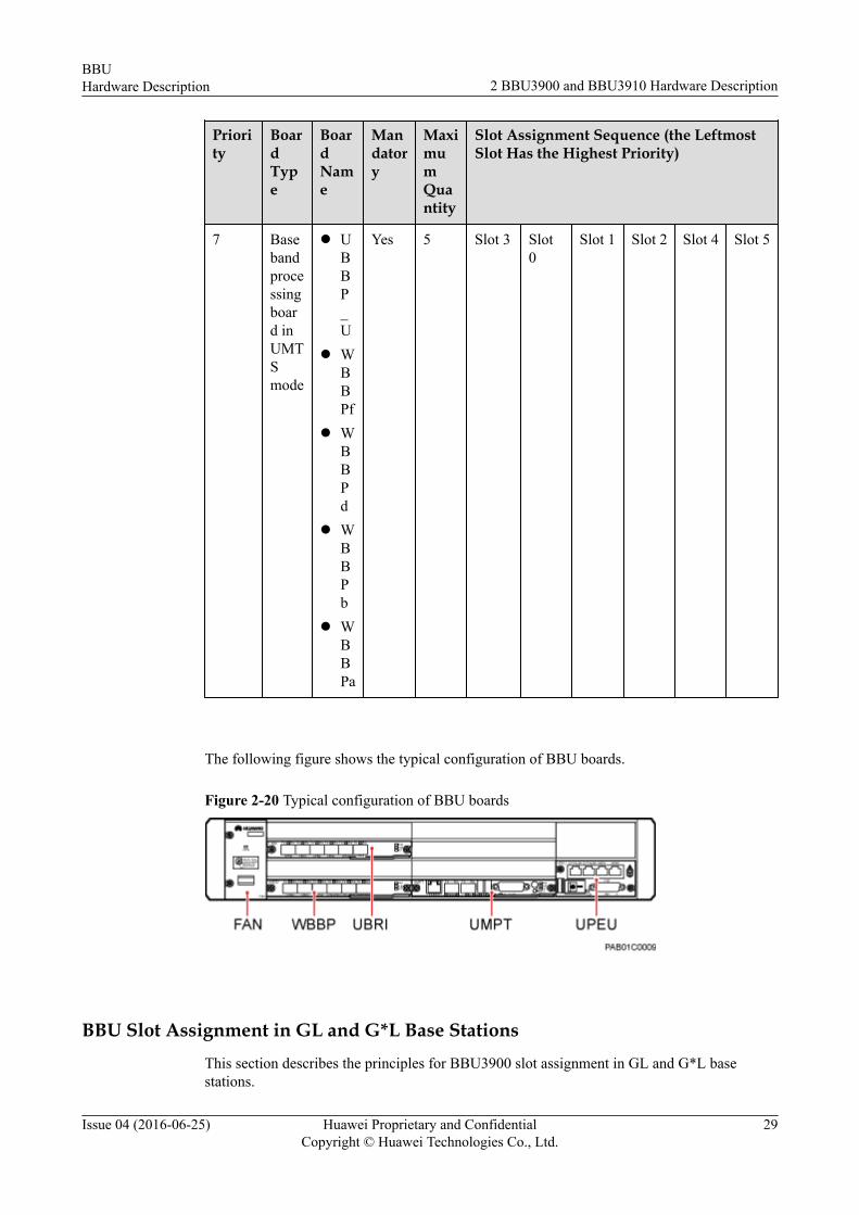
BBU Slot Assignment in GL and G*L Base Stations
This section describes the principles for BBU3900 slot assignment in GL and G*L basestations.
BBUHardware Description 2 BBU3900 and BBU3910 Hardware Description
Issue 04 (2016-06-25) Huawei Proprietary and ConfidentialCopyright © Huawei Technologies Co., Ltd.
29
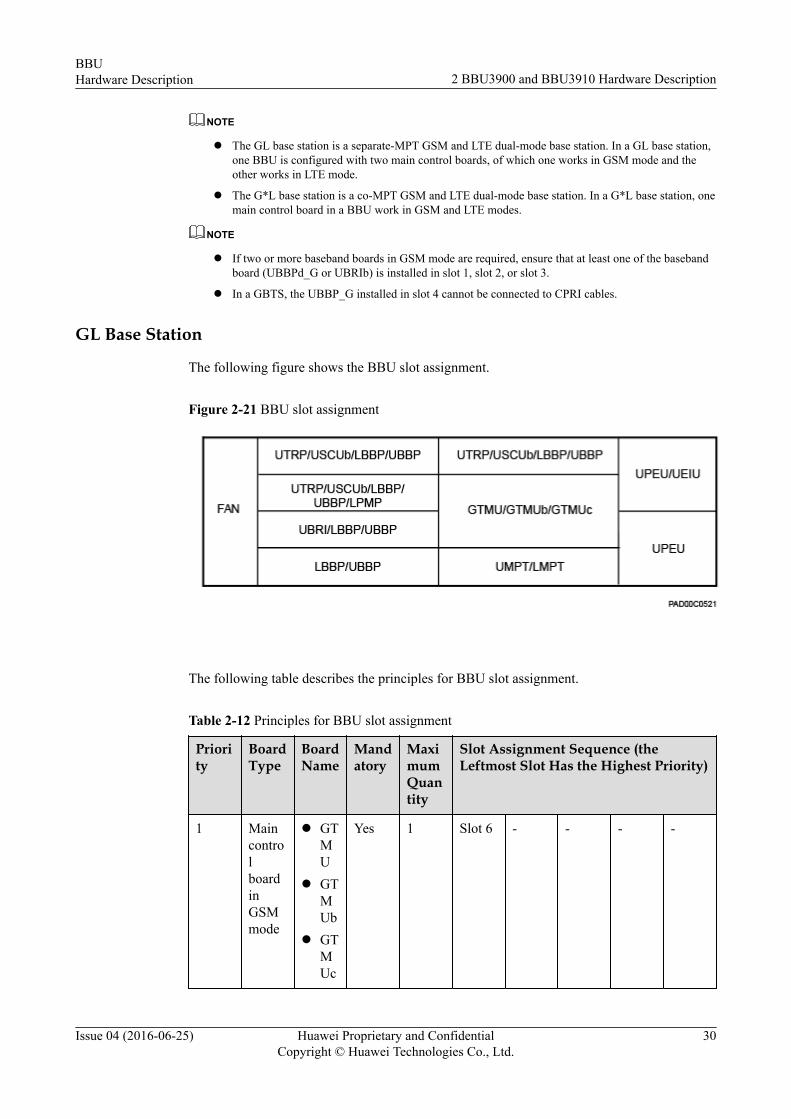
NOTE
l The GL base station is a separate-MPT GSM and LTE dual-mode base station. In a GL base station,one BBU is configured with two main control boards, of which one works in GSM mode and theother works in LTE mode.
l The G*L base station is a co-MPT GSM and LTE dual-mode base station. In a G*L base station, onemain control board in a BBU work in GSM and LTE modes.
NOTE
l If two or more baseband boards in GSM mode are required, ensure that at least one of the basebandboard (UBBPd_G or UBRIb) is installed in slot 1, slot 2, or slot 3.
l In a GBTS, the UBBP_G installed in slot 4 cannot be connected to CPRI cables.
GL Base Station
The following figure shows the BBU slot assignment.
Figure 2-21 BBU slot assignment
The following table describes the principles for BBU slot assignment.
Table 2-12 Principles for BBU slot assignment
Priority
BoardType
BoardName
Mandatory
MaximumQuantity
Slot Assignment Sequence (theLeftmost Slot Has the Highest Priority)
1 MaincontrolboardinGSMmode
l GTMU
l GTMUb
l GTMUc
Yes 1 Slot 6 - - - -
BBUHardware Description 2 BBU3900 and BBU3910 Hardware Description
Issue 04 (2016-06-25) Huawei Proprietary and ConfidentialCopyright © Huawei Technologies Co., Ltd.
30

Priority
BoardType
BoardName
Mandatory
MaximumQuantity
Slot Assignment Sequence (theLeftmost Slot Has the Highest Priority)
2 MaincontrolboardinLTEFDDmode
UMPT_L
Yes 1 Slot 7 - - - -
3 TransmissionboardinGSMmode
UTRPb4
No 1 Slot 4 Slot 0 - - -
4 Satellite-cardboard
USCUb22
No 1 Slot 1 - - - -
l USCUb14
l USCUb11
No 1 Slot 4 Slot 1 Slot 0 - -
5 BasebandradiointerfaceboardinGSMmode
l UBRI
l UBRIb
No 1 Slot 2 - - - -
6 BasebandprocessingboardinGSMmode
UBBP_G
No 2 Slot 1 Slot 2 Slot 0 Slot 4 -
BBUHardware Description 2 BBU3900 and BBU3910 Hardware Description
Issue 04 (2016-06-25) Huawei Proprietary and ConfidentialCopyright © Huawei Technologies Co., Ltd.
31

Priority
BoardType
BoardName
Mandatory
MaximumQuantity
Slot Assignment Sequence (theLeftmost Slot Has the Highest Priority)
7 InterferencecancellationboardinLTEmode
LPMP No 1 Slot 1 - - - -
8 BasebandprocessingboardinLTEFDDmodein ascenariowhereaninterferencecancellationboardisconfigured
l UBBP_L
l LBBPc
l LBBPd
Yes 4 Slot 0 Slot 3 Slot 2 Slot 4 -
BBUHardware Description 2 BBU3900 and BBU3910 Hardware Description
Issue 04 (2016-06-25) Huawei Proprietary and ConfidentialCopyright © Huawei Technologies Co., Ltd.
32
Priority
BoardType
BoardName
Mandatory
MaximumQuantity
Slot Assignment Sequence (theLeftmost Slot Has the Highest Priority)
9 BasebandprocessingboardinLTEFDDmodein ascenariowherenointerferencecancellationboardisconfigured
l UBBP_L
l LBBPc
l LBBPd
Yes 5 Slot 3 Slot 0 Slot 1 Slot 2 Slot 4
The following figure shows the typical configuration of BBU boards.
Figure 2-22 Typical configuration of BBU boards
G*L Base StationThe following figure shows the BBU slot assignment.
BBUHardware Description 2 BBU3900 and BBU3910 Hardware Description
Issue 04 (2016-06-25) Huawei Proprietary and ConfidentialCopyright © Huawei Technologies Co., Ltd.
33
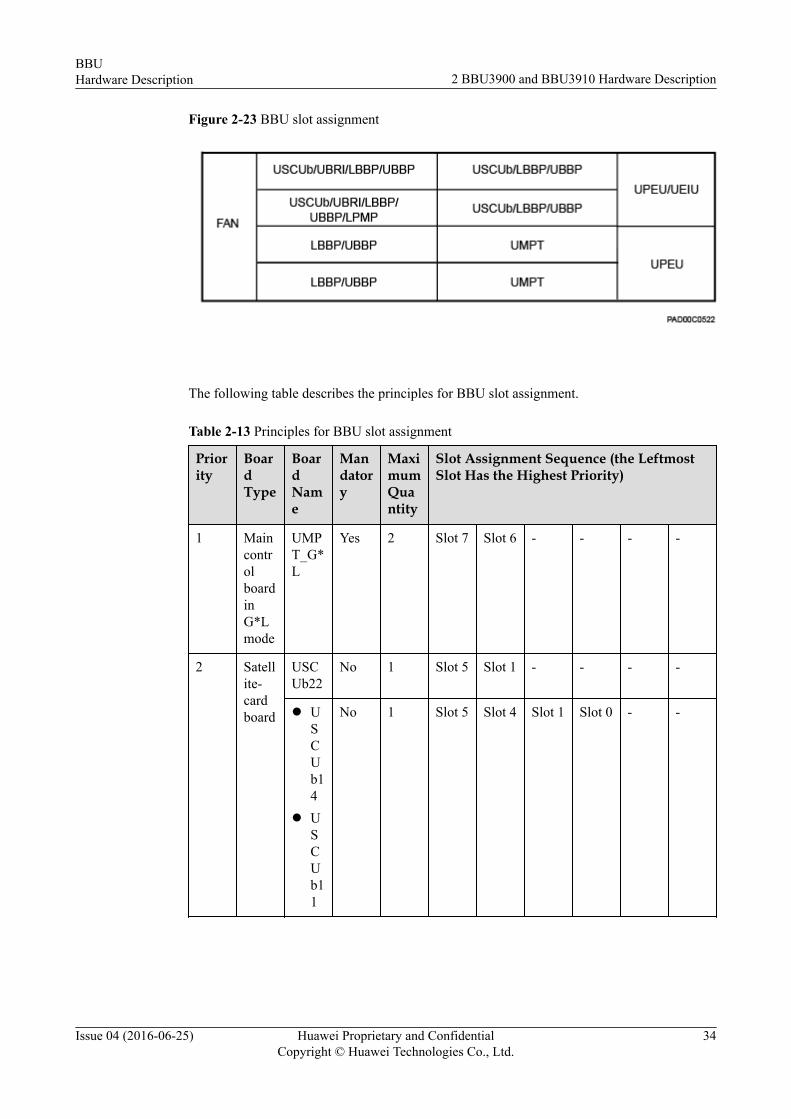
Figure 2-23 BBU slot assignment
The following table describes the principles for BBU slot assignment.
Table 2-13 Principles for BBU slot assignment
Priority
BoardType
BoardName
Mandatory
MaximumQuantity
Slot Assignment Sequence (the LeftmostSlot Has the Highest Priority)
1 MaincontrolboardinG*Lmode
UMPT_G*L
Yes 2 Slot 7 Slot 6 - - - -
2 Satellite-cardboard
USCUb22
No 1 Slot 5 Slot 1 - - - -
l USCUb14
l USCUb11
No 1 Slot 5 Slot 4 Slot 1 Slot 0 - -
BBUHardware Description 2 BBU3900 and BBU3910 Hardware Description
Issue 04 (2016-06-25) Huawei Proprietary and ConfidentialCopyright © Huawei Technologies Co., Ltd.
34

Priority
BoardType
BoardName
Mandatory
MaximumQuantity
Slot Assignment Sequence (the LeftmostSlot Has the Highest Priority)
3 Basebandprocessingboardinmultiplemodes
UBBPd_G*L
No 2 Slot 3 Slot 2 - - - -
4 BasebandradiointerfaceboardinGSMmodeormultiplemodes
l UBRIb
l UBRI
No 2 Slot 1 Slot 0 - - - -
5 BasebandprocessingboardinGSMmode
UBBP_G
No 2 Slot 1 Slot 2 Slot 0 Slot 4 Slot 5 -
6 InterferencecancellationboardinLTEmode
LPMP
No 1 Slot 1 - - - - -
BBUHardware Description 2 BBU3900 and BBU3910 Hardware Description
Issue 04 (2016-06-25) Huawei Proprietary and ConfidentialCopyright © Huawei Technologies Co., Ltd.
35
Priority
BoardType
BoardName
Mandatory
MaximumQuantity
Slot Assignment Sequence (the LeftmostSlot Has the Highest Priority)
7 BasebandprocessingboardinLTEFDDmodein ascenariowhere aninterferencecancellationboardisconfigured
l UBBP_L
l LBBPd
l LBBPc
Yes 5 Slot 0 Slot 3 Slot 2 Slot 4 Slot 5 -
BBUHardware Description 2 BBU3900 and BBU3910 Hardware Description
Issue 04 (2016-06-25) Huawei Proprietary and ConfidentialCopyright © Huawei Technologies Co., Ltd.
36

Priority
BoardType
BoardName
Mandatory
MaximumQuantity
Slot Assignment Sequence (the LeftmostSlot Has the Highest Priority)
8 BasebandprocessingboardinLTEFDDmodein ascenariowhere nointerferencecancellationboardisconfigured
l UBBP_L
l LBBPd
l LBBPc
Yes 6 Slot 3 Slot 0 Slot 1 Slot 2 Slot 4 Slot 5
The following figure shows the typical configuration of BBU boards.
Figure 2-24 Typical configuration of BBU boards
BBU Slot Assignment in UL/U*L/U*T Base StationsThis section describes the principles for BBU3900 slot assignment in UL, U*L, and U*T basestations.
BBUHardware Description 2 BBU3900 and BBU3910 Hardware Description
Issue 04 (2016-06-25) Huawei Proprietary and ConfidentialCopyright © Huawei Technologies Co., Ltd.
37

NOTE
l The UL base station is a separate-MPT GSM and LTE dual-mode base station. In a UL base station,one BBU is configured with two main control boards, of which one works in UMTS mode and theother works in LTE FDD mode.
l The U*L or U*T base station is a co-MPT base station. In a U*L or U*T base station, the maincontrol board in a BBU works in UMTS and LTE FDD modes or in UMTS and LTE TDD modes.
NOTE
l The baseband processing board in UMTS mode configured in only slot 3 can be connected to CPRIcables. A UBBP_U, WBBPd, or WBBPf is preferentially configured in slot 3. The configuration priorityof these types of boards is UBBP_U > WBBPf > WBBPd.
l If five baseband processing boards work in UMTS mode, ensure that a UBBP_U, WBBPd, or WBBPf isconfigured in slot 3.
l If slot 3 is occupied by a WBBPa or WBBPb, exchange boards to ensure that a UBBP_U, WBBPd, orWBBPf is configured in slot 3.
UL Base Station
The following figure shows the BBU slot assignment.
Figure 2-25 BBU slot assignment
The following table describes the principles for BBU slot assignment.
Table 2-14 Principles for BBU slot assignment
Priority
BoardType
BoardName
Mandatory
MaximumQuantity
Slot Assignment Sequence (theLeftmost Slot Has the Highest Priority)
1 MaincontrolboardinUMTSmode
l UMPT_U
l WMPT
Yes 1 Slot 7 - - - -
BBUHardware Description 2 BBU3900 and BBU3910 Hardware Description
Issue 04 (2016-06-25) Huawei Proprietary and ConfidentialCopyright © Huawei Technologies Co., Ltd.
38
Priority
BoardType
BoardName
Mandatory
MaximumQuantity
Slot Assignment Sequence (theLeftmost Slot Has the Highest Priority)
2 MaincontrolboardinLTEmode
l UMPT_L
l LMPT
Yes 1 Slot 6 - - - -
3 TransmissionboardinUMTSmode
UTRPc
No 1 Slot 4 Slot 5 Slot 0 Slot 1 -
l UTRP6
l UTRP9
l UTRP2
l UTRPa
l UTRP3
l UTRP4
No 2 Slot 4 Slot 5 Slot 0 Slot 1 -
4 Satellite-cardboard
USCUb22
No 1 Slot 5 Slot 1 - - -
l USCUb14
l USCUb11
No 1 Slot 5 Slot 4 Slot 1 Slot 0 -
BBUHardware Description 2 BBU3900 and BBU3910 Hardware Description
Issue 04 (2016-06-25) Huawei Proprietary and ConfidentialCopyright © Huawei Technologies Co., Ltd.
39
Priority
BoardType
BoardName
Mandatory
MaximumQuantity
Slot Assignment Sequence (theLeftmost Slot Has the Highest Priority)
5 BasebandprocessingboardinUMTSmode
l UBBP_U
l WBBPf
l WBBPd
l WBBPb
l WBBPa
Yes 5 Slot 3 Slot 0 Slot 1 Slot 4 Slot 5
6 InterferencecancellationboardinLTEmode
LPMP No 1 Slot 1 - - - -
7 BasebandprocessingboardinLTEFDDmodein ascenariowhereaninterferencecancellationboardisconfigured
l UBBP_L
l LBBPd
l LBBPc
Yes 4 Slot 0 Slot 2 Slot 4 Slot 5 -
BBUHardware Description 2 BBU3900 and BBU3910 Hardware Description
Issue 04 (2016-06-25) Huawei Proprietary and ConfidentialCopyright © Huawei Technologies Co., Ltd.
40
Priority
BoardType
BoardName
Mandatory
MaximumQuantity
Slot Assignment Sequence (theLeftmost Slot Has the Highest Priority)
8 BasebandprocessingboardinLTEFDDmodein ascenariowherenointerferencecancellationboardisconfigured
l UBBP_L
l LBBPc
l LBBPd
Yes 5 Slot 2 Slot 0 Slot 1 Slot 4 Slot 5
The following figure shows the typical configuration of BBU boards.
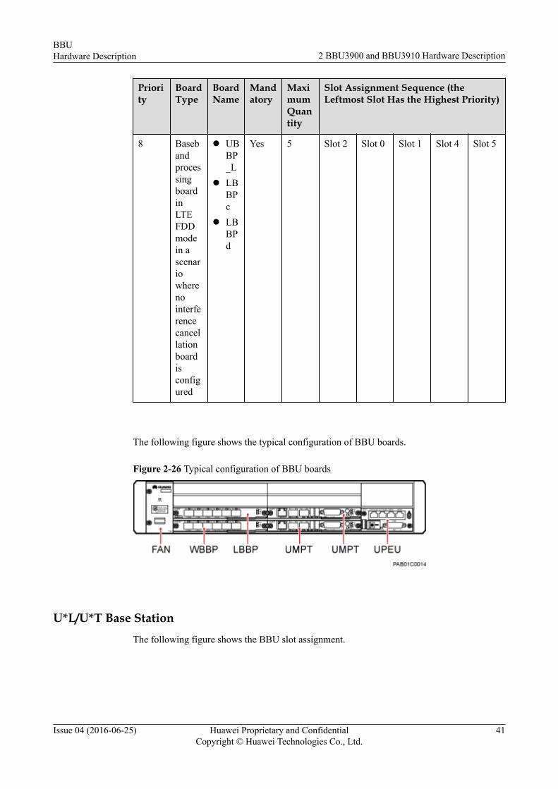
Figure 2-26 Typical configuration of BBU boards
U*L/U*T Base StationThe following figure shows the BBU slot assignment.
BBUHardware Description 2 BBU3900 and BBU3910 Hardware Description
Issue 04 (2016-06-25) Huawei Proprietary and ConfidentialCopyright © Huawei Technologies Co., Ltd.
41

Figure 2-27 BBU slot assignment
The principles for the BBU slot assignment in a U*L or U*T base station are the same asthose in a U*L base station. The following table descries the principles for BBU slotassignment in a U*L base station.
Table 2-15 Principles for BBU slot assignment
Priority
BoardType
BoardName
Mandatory
MaximumQuantity
Slot Assignment Sequence (theLeftmost Slot Has the Highest Priority)
1 MaincontrolboardinU*Lmode
UMPT_U*L
Yes 2 Slot 7 Slot 6 - - -
2 Transmissionboard
UTRPc
No 1 Slot 4 Slot 5 Slot 0 Slot 1 -
3 Satellite-cardboard
USCUb22
No 1 Slot 5 Slot 1 - - -
l USCUb14
l USCUb11
No 1 Slot 5 Slot 4 Slot 1 Slot 0 -
BBUHardware Description 2 BBU3900 and BBU3910 Hardware Description
Issue 04 (2016-06-25) Huawei Proprietary and ConfidentialCopyright © Huawei Technologies Co., Ltd.
42

Priority
BoardType
BoardName
Mandatory
MaximumQuantity
Slot Assignment Sequence (theLeftmost Slot Has the Highest Priority)
4 Basebandprocessingboardinmultiplemodes
UBBP_U*L
No 2 Slot 3 Slot 2 - - -
5 BasebandprocessingboardinUMTSmode
l UBBP_U
l WBBPf
l WBBPd
l WBBPb
l WBBPa
Yes 5 Slot 3 Slot 0 Slot 1 Slot 4 Slot 5
6 InterferencecancellationboardinLTEmode
LPMP No 1 Slot 1 - - - -
BBUHardware Description 2 BBU3900 and BBU3910 Hardware Description
Issue 04 (2016-06-25) Huawei Proprietary and ConfidentialCopyright © Huawei Technologies Co., Ltd.
43

Priority
BoardType
BoardName
Mandatory
MaximumQuantity
Slot Assignment Sequence (theLeftmost Slot Has the Highest Priority)
7 BasebandprocessingboardinLTEFDDmodein ascenariowhereaninterferencecancellationboardisconfigured
l UBBP_L
l LBBPd
l LBBPc
Yes 4 Slot 0 Slot 2 Slot 4 Slot 5 -
8 BasebandprocessingboardinLTEFDDmodein ascenariowherenointerferencecancellationboardisconfigured
l UBBP_L
l LBBPd
l LBBPc
Yes 5 Slot 2 Slot 0 Slot 1 Slot 4 Slot 5
The following figure shows the typical configuration of BBU boards.
BBUHardware Description 2 BBU3900 and BBU3910 Hardware Description
Issue 04 (2016-06-25) Huawei Proprietary and ConfidentialCopyright © Huawei Technologies Co., Ltd.
44
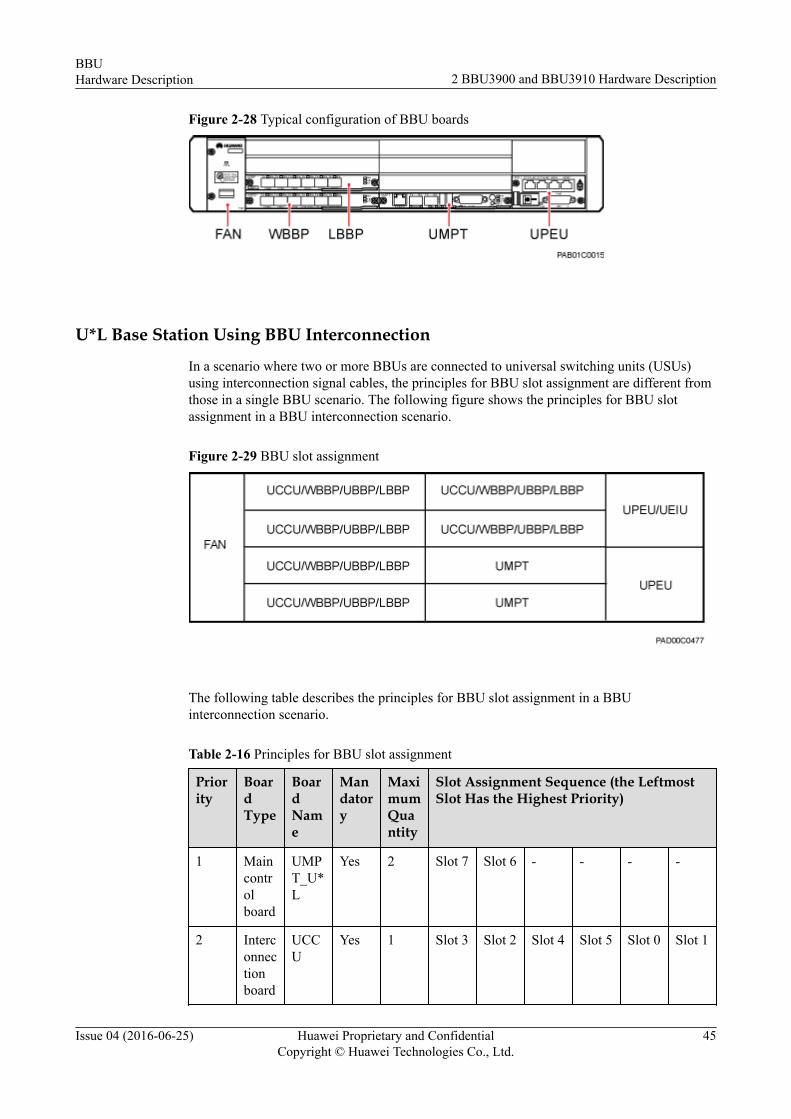
Figure 2-28 Typical configuration of BBU boards
U*L Base Station Using BBU Interconnection
In a scenario where two or more BBUs are connected to universal switching units (USUs)using interconnection signal cables, the principles for BBU slot assignment are different fromthose in a single BBU scenario. The following figure shows the principles for BBU slotassignment in a BBU interconnection scenario.
Figure 2-29 BBU slot assignment
The following table describes the principles for BBU slot assignment in a BBUinterconnection scenario.
Table 2-16 Principles for BBU slot assignment
Priority
BoardType
BoardName
Mandatory
MaximumQuantity
Slot Assignment Sequence (the LeftmostSlot Has the Highest Priority)
1 Maincontrolboard
UMPT_U*L
Yes 2 Slot 7 Slot 6 - - - -
2 Interconnectionboard
UCCU
Yes 1 Slot 3 Slot 2 Slot 4 Slot 5 Slot 0 Slot 1
BBUHardware Description 2 BBU3900 and BBU3910 Hardware Description
Issue 04 (2016-06-25) Huawei Proprietary and ConfidentialCopyright © Huawei Technologies Co., Ltd.
45

Priority
BoardType
BoardName
Mandatory
MaximumQuantity
Slot Assignment Sequence (the LeftmostSlot Has the Highest Priority)
3 BasebandprocessingboardinUMTSmode
l UBBP_U
l WBBPf
l WBBPd
Yes 6 Slot 3 Slot 2 Slot 4 Slot 5 Slot 1 Slot 0
4 BasebandprocessingboardinLTEFDDmode
l UBBP_L
l LBBPd
Yes 6 Slot 3 Slot 2 Slot 4 Slot 5 Slot 1 Slot 0
BBU Slot Assignment in Triple-Mode Base StationsThis section describes the principles for BBU3900 slot assignment in triple-mode basestations.
NOTE
l A GU+L base station is configured with two BBUs, of which one works in GU mode and the otherworks in LTE mode.
l A G[U*L] base station is configured with one BBU, which works in three modes. The BBU isconfigured with two main control boards, of which one (GTMU, GTMUb, or GTMUc) works inGSM mode and the other (UMPT) works in UMTS and LTE modes.
l A G*U*L base station is configured with one BBU, which works in three modes sharing the samemain control board.
BBUHardware Description 2 BBU3900 and BBU3910 Hardware Description
Issue 04 (2016-06-25) Huawei Proprietary and ConfidentialCopyright © Huawei Technologies Co., Ltd.
46

NOTE
l The baseband processing board in UMTS mode configured in only slot 3 can be connected to CPRIcables. A UBBP_U, WBBPd, or WBBPf is preferentially configured in slot 3. The configuration priorityof these types of boards is UBBP_U > WBBPf > WBBPd.
l If five baseband processing boards work in UMTS mode, ensure that a UBBP_U, WBBPd, or WBBPf isconfigured in slot 3.
l If slot 3 is occupied by a WBBPa or WBBPb, exchange boards to ensure that a UBBP_U, WBBPd, orWBBPf is configured in slot 3.
l If two or more baseband boards in GSM mode are required, ensure that at least one of the baseband board(UBBPd_G or UBRIb) is installed in slot 1, slot 2, or slot 3.
l In a GBTS, the UBBP_G installed in slot 4 cannot be connected to CPRI cables.
The following table describes the principles for BBU slot assignment in a triple-mode basestation.
Table 2-17 BBU slot assignment
ApplicationScenario
Description
Separate-MPTtriple-modebase stationconfiguredwith twoBBUsl GU+L base
station(BBUs notinterconnected)
l GL+U basestation(BBUs notinterconnected)
l For the BBU slot assignment for the GU mode, see BBU SlotAssignment in a GU Base Station.
l For the BBU slot assignment for the LTE mode, see BBU SlotAssignment in LTE FDD/LTE TDD Base Stations.
l For the BBU slot assignment for the GL mode, see BBU SlotAssignment in a GL Base Station.
l For the BBU slot assignment for the UMTS mode, see BBU SlotAssignment in UMTS Base Stations.
BBUHardware Description 2 BBU3900 and BBU3910 Hardware Description
Issue 04 (2016-06-25) Huawei Proprietary and ConfidentialCopyright © Huawei Technologies Co., Ltd.
47
ApplicationScenario
Description
Separate-MPTtriple-modebase stationconfiguredwith twoBBUsl GU+L base
station(BBUsinterconnected)
l GL+U basestation(BBUsinterconnected)
l GU+UL(BBUsinterconnected)
GU+L base station (BBUs interconnected)l In a BBU working in GU mode, the slot assignment for boards
(except the newly added UCIU) is the same as that in BBU SlotAssignment in a GU Base Station. The following table describes theprinciples for slot assignment for the UCIU.
l In a BBU working in LTE mode, a UMPT must be configured as themain control board. The slot assignment for other boards is the sameas that in BBU Slot Assignment in LTE FDD/LTE TDD BaseStations.
GL+U (BBUs interconnected)l In a BBU working in GL mode, the slot assignment for boards (except
the newly added UCIU) is the same as that in BBU Slot Assignmentin a GL Base Station. The following table describes the principlesfor slot assignment for the UCIU.
l In a BBU working in UMTS mode, a UMPT must be configured asthe main control board. The slot assignment for other boards is thesame as that in BBU Slot Assignment in UMTS Base Stations.
GU+UL (BBUs interconnected)l In a BBU working in GU mode, the slot assignment for boards
(except the newly added UCIU) is the same as that in BBU SlotAssignment in a GU Base Station. The following table describes theprinciples for slot assignment for the UCIU.
l In a BBU working in UMTS mode, a UMPT must be configured asthe main control board. The slot assignment for other boards is thesame as that in BBU Slot Assignment in a UL Base Station.
Separate-MPTbase stationconfiguredwith one BBUl G[U*L]
base stationl G[U*T]
base stationl G[L*T]
base stationl U[L*T]
base station
l For the BBU slot assignment in a G[U*L] or G[U*T] base station, seeG[U*L]/G[U*T] Base Station.
l For the BBU slot assignment in a G[L*T] base station, see G[L*T]Base Station.
l For the BBU slot assignment in a U[L*T] base station, see U[L*T]Base Station.
BBUHardware Description 2 BBU3900 and BBU3910 Hardware Description
Issue 04 (2016-06-25) Huawei Proprietary and ConfidentialCopyright © Huawei Technologies Co., Ltd.
48
ApplicationScenario
Description
Co-MPT basestationconfiguredwith one BBUl G*U*L
base stationl G*L*T
base station
l For the BBU slot assignment in a G*U*L base station, see G*U*LBase Station.
l For the BBU slot assignment in a G*L*T or G*L base station, seeBBU Slot Assignment in a G*L Base Station.
Co-MPT basestationconfiguredwith twoBBUs, both inG*U*L mode
For details, see G*U*L+G*U*L Base Station Using BBUInterconnection.
The following figure shows configuration principles for the UCIU.
Table 2-18 Configuration principles for the UCIU
BoardType
Board Mandatory or Not
MaximumQuantity
Slot Assignment Priorities(Descending from Left to Right)
Interconnectionboard
UCIU Yes 1 Slot 4 Slot 0 Slot 1
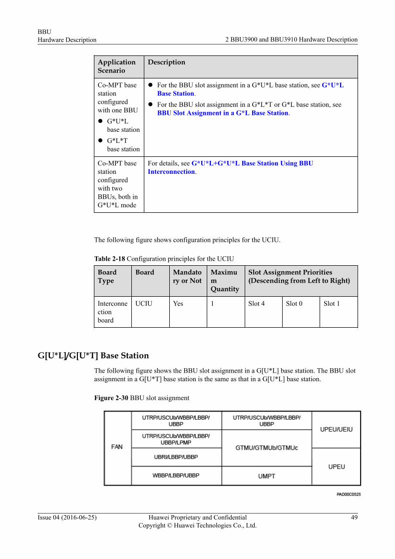
G[U*L]/G[U*T] Base StationThe following figure shows the BBU slot assignment in a G[U*L] base station. The BBU slotassignment in a G[U*T] base station is the same as that in a G[U*L] base station.
Figure 2-30 BBU slot assignment
BBUHardware Description 2 BBU3900 and BBU3910 Hardware Description
Issue 04 (2016-06-25) Huawei Proprietary and ConfidentialCopyright © Huawei Technologies Co., Ltd.
49
The following table describes the principles for BBU slot assignment in a G[U*L] basestation. The principles for the BBU slot assignment in a G[U*T] base station are the same asthose in a G[U*L] base station.
Table 2-19 Principles for BBU slot assignment
Priority
BoardType
BoardName
Mandatory
MaximumQuantity
Slot Assignment Sequence (theLeftmost Slot Has the HighestPriority)
1 MaincontrolboardinGSMmode
l GTMU
l GTMUb
l GTMUc
Yes 1 Slot 6 - - -
2 Maincontrolboardin U*Lmode
UMPT_U*L
Yes 1 Slot 7 - - -
3 TransmissionboardinGSMmode
UTRPb4
No 1 Slot 4 Slot 0 - -
4 TransmissionboardinUMTSmode
UTRPc No 1 Slot 4 Slot 0 Slot 1 -
l UTRP6
l UTRP9
l UTRP2
l UTRPa
l UTRP3
l UTRP4
No 2 Slot 4 Slot 0 Slot 1 -
5 Satellite-cardboard
USCUb22
No 1 Slot 1 - - -
BBUHardware Description 2 BBU3900 and BBU3910 Hardware Description
Issue 04 (2016-06-25) Huawei Proprietary and ConfidentialCopyright © Huawei Technologies Co., Ltd.
50
Priority
BoardType
BoardName
Mandatory
MaximumQuantity
Slot Assignment Sequence (theLeftmost Slot Has the HighestPriority)
l USCUb14
l USCUb11
No 1 Slot 4 Slot 1 Slot 0 -
6 Basebandprocessingboardinmultiplemodes
UBBP_U*L
No 2 Slot 3 Slot 2 - -
7 Basebandradiointerface boardinGSMmodeormultiplemodes
l UBRIb
l UBRI
Yes 1 Slot 2 - - -
8 BasebandprocessingboardinGSMmode
UBBP_G
Yes 2 Slot 1 Slot 0 Slot 4 -
BBUHardware Description 2 BBU3900 and BBU3910 Hardware Description
Issue 04 (2016-06-25) Huawei Proprietary and ConfidentialCopyright © Huawei Technologies Co., Ltd.
51
Priority
BoardType
BoardName
Mandatory
MaximumQuantity
Slot Assignment Sequence (theLeftmost Slot Has the HighestPriority)
9 BasebandprocessingboardinUMTSmode
l UBBP_U
l WBBPf
l WBBPd
l WBBPb
l WBBPa
Yes 4 Slot 3 Slot 0 Slot 1 Slot 4
10 Interferencecancellationboardin LTEmode
LPMP No 1 Slot 1 - - -
11 Basebandprocessingboardin LTEFDDmodein ascenariowhereaninterferencecancellationboardisconfigured
l UBBP_L
l LBBPd
l LBBPc
Yes 3 Slot 0 Slot 2 Slot 4 -
BBUHardware Description 2 BBU3900 and BBU3910 Hardware Description
Issue 04 (2016-06-25) Huawei Proprietary and ConfidentialCopyright © Huawei Technologies Co., Ltd.
52
Priority
BoardType
BoardName
Mandatory
MaximumQuantity
Slot Assignment Sequence (theLeftmost Slot Has the HighestPriority)
12 Basebandprocessingboardin LTEFDDmodein ascenariowherenointerferencecancellationboardisconfigured
l UBBP_L
l LBBPd
l LBBPc
Yes 4 Slot 2 Slot 0 Slot 1 Slot 4
The following figure shows the typical configuration of BBU boards.
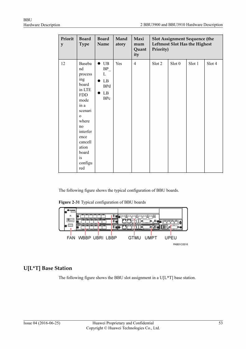
Figure 2-31 Typical configuration of BBU boards
U[L*T] Base StationThe following figure shows the BBU slot assignment in a U[L*T] base station.
BBUHardware Description 2 BBU3900 and BBU3910 Hardware Description
Issue 04 (2016-06-25) Huawei Proprietary and ConfidentialCopyright © Huawei Technologies Co., Ltd.
53
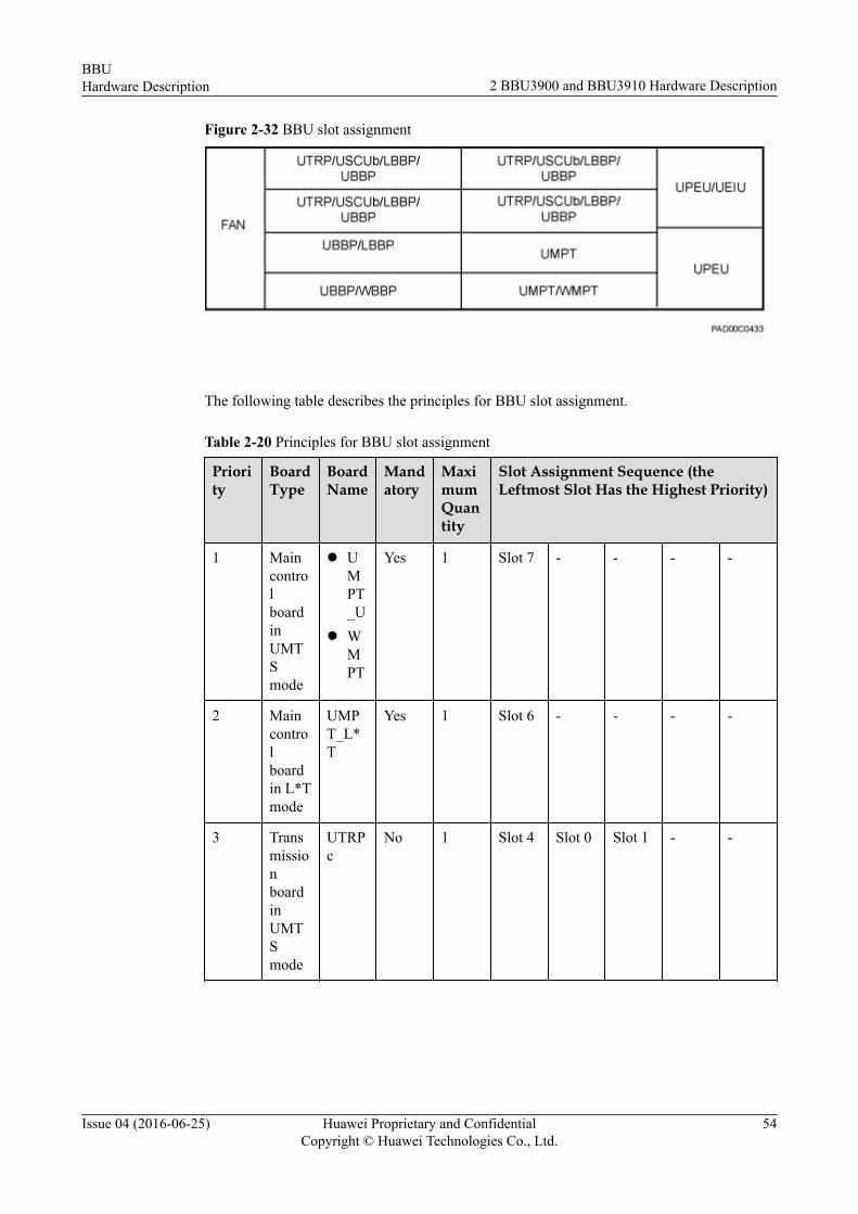
Figure 2-32 BBU slot assignment
The following table describes the principles for BBU slot assignment.
Table 2-20 Principles for BBU slot assignment
Priority
BoardType
BoardName
Mandatory
MaximumQuantity
Slot Assignment Sequence (theLeftmost Slot Has the Highest Priority)
1 MaincontrolboardinUMTSmode
l UMPT_U
l WMPT
Yes 1 Slot 7 - - - -
2 Maincontrolboardin L*Tmode
UMPT_L*T
Yes 1 Slot 6 - - - -
3 TransmissionboardinUMTSmode
UTRPc
No 1 Slot 4 Slot 0 Slot 1 - -
BBUHardware Description 2 BBU3900 and BBU3910 Hardware Description
Issue 04 (2016-06-25) Huawei Proprietary and ConfidentialCopyright © Huawei Technologies Co., Ltd.
54

Priority
BoardType
BoardName
Mandatory
MaximumQuantity
Slot Assignment Sequence (theLeftmost Slot Has the Highest Priority)
l UTRP6
l UTRP9
l UTRP2
l UTRPa
l UTRP3
l UTRP4
No 2 Slot 4 Slot 0 Slot 1 - -
4 Satellite-cardboard
USCUb22
No 1 Slot 1 - - - -
l USCUb14
l USCUb11
No 1 Slot 4 Slot 1 Slot 0 - -
BBUHardware Description 2 BBU3900 and BBU3910 Hardware Description
Issue 04 (2016-06-25) Huawei Proprietary and ConfidentialCopyright © Huawei Technologies Co., Ltd.
55

Priority
BoardType
BoardName
Mandatory
MaximumQuantity
Slot Assignment Sequence (theLeftmost Slot Has the Highest Priority)
5 BasebandprocessingboardinUMTSmode
l UBBP_U
l WBBPf
l WBBPd
l WBBPb
l WBBPa
Yes 4 Slot 3 Slot 0 Slot 1 Slot 4 Slot 5
6 BasebandprocessingboardinLTEFDDmode
l UBBP_L
l LBBPd_L
Yes 4 Slot 2 Slot 0 Slot 1 Slot 4 Slot 5
7 BasebandprocessingboardinLTETDDmode
l UBBP_T
l LBBPd_T
Yes 4 Slot 2 Slot 0 Slot 1 Slot 4 Slot 5
The following figure shows the typical configuration of BBU boards.
BBUHardware Description 2 BBU3900 and BBU3910 Hardware Description
Issue 04 (2016-06-25) Huawei Proprietary and ConfidentialCopyright © Huawei Technologies Co., Ltd.
56
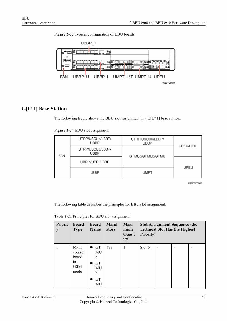
Figure 2-33 Typical configuration of BBU boards
G[L*T] Base Station
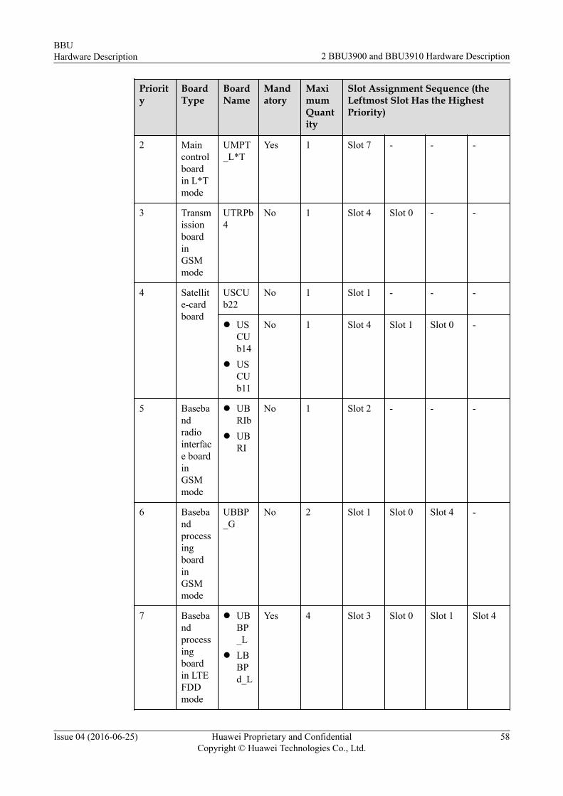
The following figure shows the BBU slot assignment in a G[L*T] base station.
Figure 2-34 BBU slot assignment
The following table describes the principles for BBU slot assignment.
Table 2-21 Principles for BBU slot assignment
Priority
BoardType
BoardName
Mandatory
MaximumQuantity
Slot Assignment Sequence (theLeftmost Slot Has the HighestPriority)
1 MaincontrolboardinGSMmode
l GTMUc
l GTMUb
l GTMU
Yes 1 Slot 6 - - -
BBUHardware Description 2 BBU3900 and BBU3910 Hardware Description
Issue 04 (2016-06-25) Huawei Proprietary and ConfidentialCopyright © Huawei Technologies Co., Ltd.
57
Priority
BoardType
BoardName
Mandatory
MaximumQuantity
Slot Assignment Sequence (theLeftmost Slot Has the HighestPriority)
2 Maincontrolboardin L*Tmode
UMPT_L*T
Yes 1 Slot 7 - - -
3 TransmissionboardinGSMmode
UTRPb4
No 1 Slot 4 Slot 0 - -
4 Satellite-cardboard
USCUb22
No 1 Slot 1 - - -
l USCUb14
l USCUb11
No 1 Slot 4 Slot 1 Slot 0 -
5 Basebandradiointerface boardinGSMmode
l UBRIb
l UBRI
No 1 Slot 2 - - -
6 BasebandprocessingboardinGSMmode
UBBP_G
No 2 Slot 1 Slot 0 Slot 4 -
7 Basebandprocessingboardin LTEFDDmode
l UBBP_L
l LBBPd_L
Yes 4 Slot 3 Slot 0 Slot 1 Slot 4
BBUHardware Description 2 BBU3900 and BBU3910 Hardware Description
Issue 04 (2016-06-25) Huawei Proprietary and ConfidentialCopyright © Huawei Technologies Co., Ltd.
58

Priority
BoardType
BoardName
Mandatory
MaximumQuantity
Slot Assignment Sequence (theLeftmost Slot Has the HighestPriority)
8 Basebandprocessingboardin LTETDDmode
l UBBP_T
l LBBPd_T
Yes 4 Slot 2 Slot 0 Slot 1 Slot 4
The following figure shows the typical configuration of BBU boards.
Figure 2-35 Typical configuration of BBU boards
G*U*L Base StationThe following figure shows the BBU slot assignment.
Figure 2-36 BBU slot assignment
BBUHardware Description 2 BBU3900 and BBU3910 Hardware Description
Issue 04 (2016-06-25) Huawei Proprietary and ConfidentialCopyright © Huawei Technologies Co., Ltd.
59

The following table describes the principles for BBU slot assignment.
Table 2-22 Principles for BBU slot assignment
Priority
BoardType
BoardName
Mandatory
MaximumQuantity
Slot Assignment Sequence (theLeftmost Slot Has the Highest Priority)
1 Maincontrolboard
UMPT_G*U*L
Yes 2 Slot 7 Slot 6 - - -
2 Transmissionboard
UTRPc
No 1 Slot 4 Slot 5 Slot 0 Slot 1 -
3 Satellite-cardboard
USCUb22
No 1 Slot 5 Slot 1 - - -
l USCUb14
l USCUb11
No 1 Slot 5 Slot 4 Slot 1 Slot 0 -
4 Basebandprocessingboardinmultiplemodes
UBBP_G*U*L
No 2 Slot 3 Slot 2 - - -
5 BasebandradiointerfaceboardinGSMmodeormultiplemodes
l UBRIb
l UBRI
No 2 Slot 1 Slot 0 - - -
BBUHardware Description 2 BBU3900 and BBU3910 Hardware Description
Issue 04 (2016-06-25) Huawei Proprietary and ConfidentialCopyright © Huawei Technologies Co., Ltd.
60
Priority
BoardType
BoardName
Mandatory
MaximumQuantity
Slot Assignment Sequence (theLeftmost Slot Has the Highest Priority)
6 BasebandprocessingboardinGSMmode
UBBP_G
No 2 Slot 1 Slot 2 Slot 0 Slot 4 Slot 5
7 BasebandprocessingboardinUMTSmode
l UBBP_U
l WBBPf
l WBBPd
l WBBPb
l WBBPa
Yes 5 Slot 3 Slot 0 Slot 1 Slot 4 Slot 5
8 InterferencecancellationboardinLTEmode
LPMP No 1 Slot 1 - - - -
BBUHardware Description 2 BBU3900 and BBU3910 Hardware Description
Issue 04 (2016-06-25) Huawei Proprietary and ConfidentialCopyright © Huawei Technologies Co., Ltd.
61
Priority
BoardType
BoardName
Mandatory
MaximumQuantity
Slot Assignment Sequence (theLeftmost Slot Has the Highest Priority)
9 BasebandprocessingboardinLTEFDDmodein ascenariowhereaninterferencecancellationboardisconfigured
l UBBP_L
l LBBPc
l LBBPd
Yes 4 Slot 0 Slot 2 Slot 4 Slot 5 -
10 BasebandprocessingboardinLTEFDDmodein ascenariowherenointerferencecancellationboardisconfigured
l UBBP_L
l LBBPc
l LBBPd
Yes 5 Slot 2 Slot 0 Slot 1 Slot 4 Slot 5
The following figure shows the typical configuration of BBU boards.
BBUHardware Description 2 BBU3900 and BBU3910 Hardware Description
Issue 04 (2016-06-25) Huawei Proprietary and ConfidentialCopyright © Huawei Technologies Co., Ltd.
62

Figure 2-37 Typical configuration of BBU boards
G*U*L+G*U*L Base Station Using BBU InterconnectionThe following figure shows the BBU slot assignment in two interconnected BBUs in G*U*L+G*U*L mode.
Figure 2-38 BBU slot assignment in a G*U*L+G*U*L base station Using BBUInterconnection
BBU Slot Assignment in Quadruple-Mode Base StationsThis section describes the principles for BBU3900 slot assignment in quadruple-mode basestations.
BBUHardware Description 2 BBU3900 and BBU3910 Hardware Description
Issue 04 (2016-06-25) Huawei Proprietary and ConfidentialCopyright © Huawei Technologies Co., Ltd.
63
NOTE
l The baseband processing board in UMTS mode configured in only slot 3 can be connected to CPRIcables. A UBBP_U, WBBPd, or WBBPf is preferentially configured in slot 3. The configuration priorityof these types of boards is UBBP_U > WBBPf > WBBPd.
l If five baseband processing boards work in UMTS mode, ensure that a UBBP_U, WBBPd, or WBBPf isconfigured in slot 3.
l If slot 3 is occupied by a WBBPa or WBBPb, exchange boards to ensure that a UBBP_U, WBBPd, orWBBPf is configured in slot 3.
l If two or more baseband boards in GSM mode are required, ensure that at least one of the baseband board(UBBPd_G or UBRIb) is installed in slot 1, slot 2, or slot 3.
l In a GBTS, the UBBP_G installed in slot 4 cannot be connected to CPRI cables.
The following table describes the BBU slot assignment in quadruple-mode base stations.
Table 2-23 BBU slot assignment
Application Scenario Description
Separate-MPTquadruple-mode basestation configured withtwo BBUs:l GU+L*T base station
(UCIU+UMPT)
GU+L*T base station (UCIU+UMPT):l In a BBU working in GU mode, the slot assignment for
boards (except the newly added UCIU) is the same as thatin BBU Slot Assignment in a GU Base Station. Thefollowing table describes the principles for slot assignmentfor the UCIU.
l For the BBU slot assignment for the L*T mode, see BBUSlot Assignment in an L*T Base Station.
Co-MPT quadruple-mode base stationconfigured with oneBBU: G*U*L*T basestation
For the BBU slot assignment in a G*U*L*T base station, seeG*U*L*T Base Station.
The following figure shows configuration principles for the UCIU.
Table 2-24 Configuration principles for the UCIU
BoardType
Board Mandatory or Not
MaximumQuantity
Slot Assignment Priorities(Descending from Left to Right)
Interconnectionboard
UCIU Yes 1 Slot 4 Slot 0 Slot 1
G*U*L*T Base Station
The following figure shows the BBU slot assignment in a G*U*L*T base station.
BBUHardware Description 2 BBU3900 and BBU3910 Hardware Description
Issue 04 (2016-06-25) Huawei Proprietary and ConfidentialCopyright © Huawei Technologies Co., Ltd.
64

Figure 2-39 BBU slot assignment
The following table describes the principles for BBU slot assignment.
Table 2-25 Principles for BBU slot assignment
Priority
BoardType
BoardName
Mandatory
MaximumQuantity
Slot Assignment Sequence (theLeftmost Slot Has the Highest Priority)
1 Maincontrolboard
UMPT_G*U*L*T
Yes 2 Slot 7 Slot 6 - - -
2 Transmissionboard
UTRPc
No 1 Slot 4 Slot 5 Slot 0 Slot 1 -
3 Satellite-cardboard
USCUb22
No 1 Slot 5 Slot 1 - - -
l USCUb14
l USCUb11
No 1 Slot 5 Slot 4 Slot 1 Slot 0 -
BBUHardware Description 2 BBU3900 and BBU3910 Hardware Description
Issue 04 (2016-06-25) Huawei Proprietary and ConfidentialCopyright © Huawei Technologies Co., Ltd.
65
Priority
BoardType
BoardName
Mandatory
MaximumQuantity
Slot Assignment Sequence (theLeftmost Slot Has the Highest Priority)
4 Basebandprocessingboardinmultiplemodes
UBBP_G*U*L*T
No 2 Slot 3 Slot 2 - - -
5 BasebandradiointerfaceboardinGSMmodeormultiplemodes
l UBRI
l UBRIb
No 2 Slot 1 Slot 0 - - -
6 BasebandprocessingboardinUMTSmode
l UBBP_U
l WBBPf
l WBBPd
l WBBPb
l WBBPa
Yes 5 Slot 3 Slot 0 Slot 1 Slot 4 Slot 5
BBUHardware Description 2 BBU3900 and BBU3910 Hardware Description
Issue 04 (2016-06-25) Huawei Proprietary and ConfidentialCopyright © Huawei Technologies Co., Ltd.
66

Priority
BoardType
BoardName
Mandatory
MaximumQuantity
Slot Assignment Sequence (theLeftmost Slot Has the Highest Priority)
7 InterferencecancellationboardinLTEmode
LPMP No 1 Slot 1 - - - -
8 BasebandprocessingboardinLTEFDDmodein ascenariowhereaninterferencecancellationboardisconfigured
l UBBP_L
l LBBPd_L
Yes 4 Slot 2 Slot 0 Slot 1 - -
BBUHardware Description 2 BBU3900 and BBU3910 Hardware Description
Issue 04 (2016-06-25) Huawei Proprietary and ConfidentialCopyright © Huawei Technologies Co., Ltd.
67
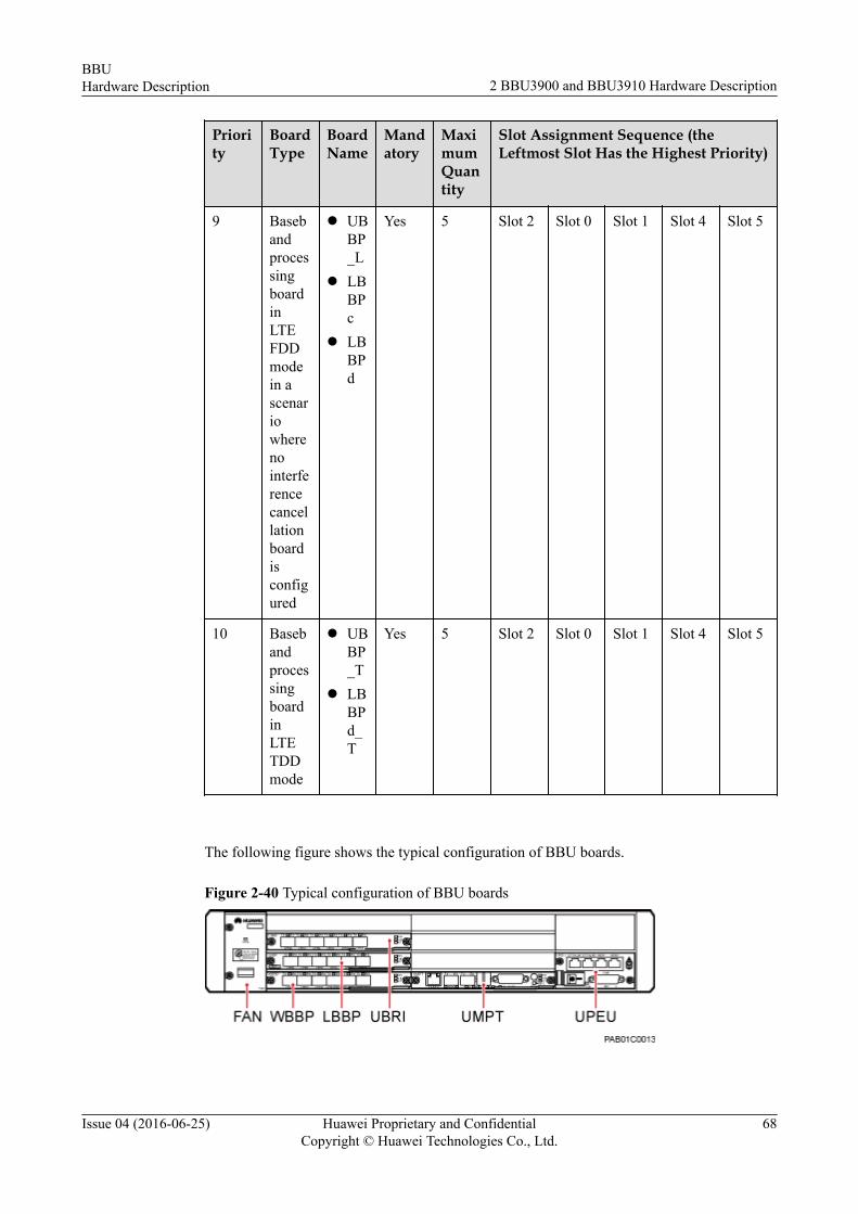
Priority
BoardType
BoardName
Mandatory
MaximumQuantity
Slot Assignment Sequence (theLeftmost Slot Has the Highest Priority)
9 BasebandprocessingboardinLTEFDDmodein ascenariowherenointerferencecancellationboardisconfigured
l UBBP_L
l LBBPc
l LBBPd
Yes 5 Slot 2 Slot 0 Slot 1 Slot 4 Slot 5
10 BasebandprocessingboardinLTETDDmode
l UBBP_T
l LBBPd_T
Yes 5 Slot 2 Slot 0 Slot 1 Slot 4 Slot 5
The following figure shows the typical configuration of BBU boards.
Figure 2-40 Typical configuration of BBU boards
BBUHardware Description 2 BBU3900 and BBU3910 Hardware Description
Issue 04 (2016-06-25) Huawei Proprietary and ConfidentialCopyright © Huawei Technologies Co., Ltd.
68

2.4.3 BBU3910 Slot AssignmentThis section describes the principles for BBU3910 slot assignment.
BBU Slot Assignment in GSM Base StationsThis section describes the principles for BBU3910 slot assignment in GSM base stations.
GBTSThe following figure shows the BBU slot assignment in a GBTS.
Figure 2-41 BBU slot assignment
The following table describes the principles for BBU slot assignment.
Table 2-26 Principles for BBU slot assignment
Priority
BoardType
BoardName
Mandatory
MaximumQuantity
Slot Assignment Sequence (theLeftmost Slot Has the Highest Priority)
1 Maincontrolboard
l GTMUb
l GTMUc
Yes 1 Slot 6 - - - -
2 Satellite-cardboard
USCUb14
No 1 Slot 4 Slot 1 Slot 0 - -
BBUHardware Description 2 BBU3900 and BBU3910 Hardware Description
Issue 04 (2016-06-25) Huawei Proprietary and ConfidentialCopyright © Huawei Technologies Co., Ltd.
69
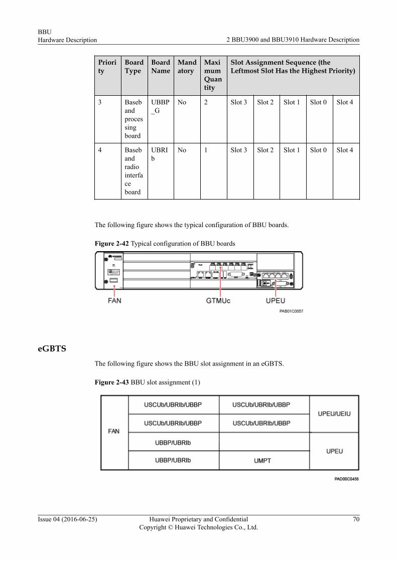
Priority
BoardType
BoardName
Mandatory
MaximumQuantity
Slot Assignment Sequence (theLeftmost Slot Has the Highest Priority)
3 Basebandprocessingboard
UBBP_G
No 2 Slot 3 Slot 2 Slot 1 Slot 0 Slot 4
4 Basebandradiointerfaceboard
UBRIb
No 1 Slot 3 Slot 2 Slot 1 Slot 0 Slot 4
The following figure shows the typical configuration of BBU boards.
Figure 2-42 Typical configuration of BBU boards
eGBTSThe following figure shows the BBU slot assignment in an eGBTS.
Figure 2-43 BBU slot assignment (1)
BBUHardware Description 2 BBU3900 and BBU3910 Hardware Description
Issue 04 (2016-06-25) Huawei Proprietary and ConfidentialCopyright © Huawei Technologies Co., Ltd.
70

Figure 2-44 BBU slot assignment (2)
The following table describes the principles for BBU slot assignment.
Table 2-27 Principles for BBU slot assignment
Priority
BoardType
BoardName
Mandatory
MaximumQuantity
Slot Assignment Sequence (the LeftmostSlot Has the Highest Priority)
1 Maincontrolboard
UMPT_G
Yes 1 Slot 7 - - - - -
l GTMUb
l GTMUc
1 Slot 6 - - - - -
2 Satellite-cardboard
USCUb14
No 1 Slot 5 Slot 4 Slot 1 Slot 0 - -
3 Basebandprocessingboard
UBBP_G
No 2 Slot 3 Slot 2 Slot 1 Slot 0 Slot 4 Slot 5
BBUHardware Description 2 BBU3900 and BBU3910 Hardware Description
Issue 04 (2016-06-25) Huawei Proprietary and ConfidentialCopyright © Huawei Technologies Co., Ltd.
71
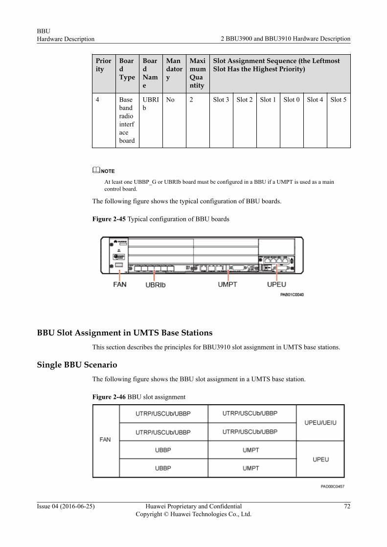
Priority
BoardType
BoardName
Mandatory
MaximumQuantity
Slot Assignment Sequence (the LeftmostSlot Has the Highest Priority)
4 Basebandradiointerfaceboard
UBRIb
No 2 Slot 3 Slot 2 Slot 1 Slot 0 Slot 4 Slot 5
NOTE
At least one UBBP_G or UBRIb board must be configured in a BBU if a UMPT is used as a maincontrol board.
The following figure shows the typical configuration of BBU boards.
Figure 2-45 Typical configuration of BBU boards
BBU Slot Assignment in UMTS Base StationsThis section describes the principles for BBU3910 slot assignment in UMTS base stations.
Single BBU ScenarioThe following figure shows the BBU slot assignment in a UMTS base station.
Figure 2-46 BBU slot assignment
BBUHardware Description 2 BBU3900 and BBU3910 Hardware Description
Issue 04 (2016-06-25) Huawei Proprietary and ConfidentialCopyright © Huawei Technologies Co., Ltd.
72

The following table describes the principles for BBU slot assignment in a UMTS base station.
Table 2-28 Principles for BBU slot assignment
Priority
BoardType
BoardName
Mandatory
MaximumQuantity
Slot Assignment Sequence (the LeftmostSlot Has the Highest Priority)
1 Maincontrolboard
UMPT_U
Yes 2 Slot 7 Slot 6 - - - -
2 Transmissionboard
UTRPc
No 1 Slot 5 Slot 4 Slot 0 Slot 1 - -
UTRPa
No 2 Slot 5 Slot 4 Slot 0 Slot 1 - -
3 Satellite-cardboard
USCUb14
No 1 Slot 5 Slot 4 Slot 1 Slot 0 - -
4 Basebandprocessingboard
UBBP_U
Yes 6 Slot 3 Slot 2 Slot 1 Slot 0 Slot 4 Slot 5
The following figure shows the typical configuration of BBU boards.
Figure 2-47 Typical configuration of BBU boards
BBU Interconnection ScenarioIn a scenario where two or more BBUs are connected to universal switching units (USUs)using interconnection signal cables, the principles for BBU slot assignment are different from
BBUHardware Description 2 BBU3900 and BBU3910 Hardware Description
Issue 04 (2016-06-25) Huawei Proprietary and ConfidentialCopyright © Huawei Technologies Co., Ltd.
73

those in a single BBU scenario. The following figure shows the principles for BBU slotassignment in a BBU interconnection scenario.
Figure 2-48 BBU slot assignment
The following table describes the principles for BBU slot assignment in a BBUinterconnection scenario.
Table 2-29 Principles for BBU slot assignment
Priority
BoardType
BoardName
Mandatory
MaximumQuantity
Slot Assignment Sequence (the LeftmostSlot Has the Highest Priority)
1 Maincontrolboard
UMPT_U
Yes 2 Slot 7 Slot 6 - - - -
2 Interconnectionboard
UCCU
Yes 1 Slot 3 Slot 2 Slot 1 Slot 0 Slot 4 Slot 5
3 Basebandprocessingboard
UBBP_U
Yes 6 Slot 3 Slot 2 Slot 1 Slot 0 Slot 4 Slot 5
BBU Slot Assignment in LTE FDD/LTE TDD Base StationsThis section describes the principles for BBU3910 slot assignment in LTE FDD and LTETDD base stations.
BBUHardware Description 2 BBU3900 and BBU3910 Hardware Description
Issue 04 (2016-06-25) Huawei Proprietary and ConfidentialCopyright © Huawei Technologies Co., Ltd.
74

Single BBU Scenario
The principles for BBU slot assignment in an LTE FDD base station are the same as those inan LTE TDD base station. This section uses the BBU slot assignment in an LTE FDD basestation as an example. The following figure shows the BBU slot assignment.
Figure 2-49 BBU slot assignment
The following table describes the principles for BBU slot assignment.
Table 2-30 Principles for BBU slot assignment
Priority
BoardType
BoardName
Mandatory
MaximumQuantity
Slot Assignment Sequence (the LeftmostSlot Has the Highest Priority)
1 MaincontrolboardinLTEFDDmode
UMPT_L
Yes 2 Slot7
Slot 6 - - - -
2 Satellite-cardboard
l USCUb14
l USCUb11
No 1 Slot5
Slot 4 Slot 1 Slot 0 - -
BBUHardware Description 2 BBU3900 and BBU3910 Hardware Description
Issue 04 (2016-06-25) Huawei Proprietary and ConfidentialCopyright © Huawei Technologies Co., Ltd.
75

Priority
BoardType
BoardName
Mandatory
MaximumQuantity
Slot Assignment Sequence (the LeftmostSlot Has the Highest Priority)
3 InterferencecancellationboardinLTEmode
LPMP
No 1 Slot2
- - - - -
4 BasebandprocessingboardinLTEFDDmode
UBBP_L
Yes 6 Slot3
Slot 2 Slot 1 Slot 0 Slot 4 Slot 5
The following figure shows the typical configuration of BBU boards.
Figure 2-50 Typical configuration of BBU boards
BBU Interconnection ScenarioIn a scenario where two or more BBUs are connected to universal switching units (USUs)using interconnection signal cables, the principles for BBU slot assignment are different fromthose in a single BBU scenario. The following figure shows the principles for BBU slotassignment in a BBU interconnection scenario.
BBUHardware Description 2 BBU3900 and BBU3910 Hardware Description
Issue 04 (2016-06-25) Huawei Proprietary and ConfidentialCopyright © Huawei Technologies Co., Ltd.
76

Figure 2-51 BBU slot assignment
The following table describes the principles for BBU slot assignment in a BBUinterconnection scenario.
Table 2-31 Principles for BBU slot assignment
Priority
BoardType
BoardName
Mandatory
MaximumQuantity
Slot Assignment Sequence (the LeftmostSlot Has the Highest Priority)
1 Maincontrolboard
UMPT_L
Yes 2 Slot 7 Slot 6 - - - -
2 Interconnectionboard
UCCU
Yes 1 Slot 3 Slot 2 Slot 1 Slot 0 Slot 4 Slot 5
3 Basebandprocessingboard
UBBP_L
Yes 6 Slot 3 Slot 2 Slot 1 Slot 0 Slot 4 Slot 5
BBU Slot Assignment in GU and G*U Base StationsThis section describes the principles for BBU3910 slot assignment in GU and G*U basestations.
GU Base StationThe following figure shows the BBU slot assignment in a GU base station.
BBUHardware Description 2 BBU3900 and BBU3910 Hardware Description
Issue 04 (2016-06-25) Huawei Proprietary and ConfidentialCopyright © Huawei Technologies Co., Ltd.
77

Figure 2-52 BBU slot assignment
The following table describes the principles for BBU slot assignment.
Table 2-32 Principles for BBU slot assignment
Priority
BoardType
BoardName
Mandatory
MaximumQuantity
Slot Assignment Sequence (theLeftmost Slot Has the Highest Priority)
1 MaincontrolboardinGSMmode
l GTMUb
l GTMUc
Yes 1 Slot 6 - - - -
2 MaincontrolboardinUMTSmode
UMPT_U
Yes 1 Slot 7 - - - -
3 TransmissionboardinUMTSmode
UTRPc
No 1 Slot 4 Slot 0 Slot 1 - -
UTRPa
No 2 Slot 4 Slot 0 Slot 1 - -
BBUHardware Description 2 BBU3900 and BBU3910 Hardware Description
Issue 04 (2016-06-25) Huawei Proprietary and ConfidentialCopyright © Huawei Technologies Co., Ltd.
78
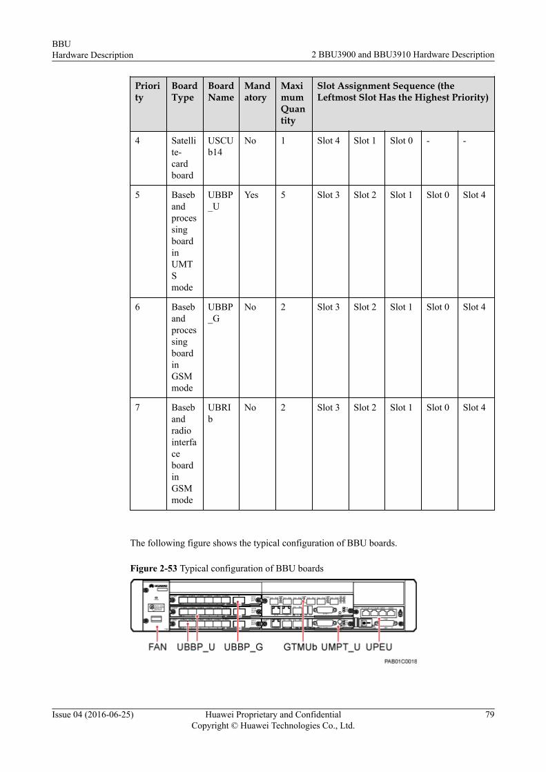
Priority
BoardType
BoardName
Mandatory
MaximumQuantity
Slot Assignment Sequence (theLeftmost Slot Has the Highest Priority)
4 Satellite-cardboard
USCUb14
No 1 Slot 4 Slot 1 Slot 0 - -
5 BasebandprocessingboardinUMTSmode
UBBP_U
Yes 5 Slot 3 Slot 2 Slot 1 Slot 0 Slot 4
6 BasebandprocessingboardinGSMmode
UBBP_G
No 2 Slot 3 Slot 2 Slot 1 Slot 0 Slot 4
7 BasebandradiointerfaceboardinGSMmode
UBRIb
No 2 Slot 3 Slot 2 Slot 1 Slot 0 Slot 4
The following figure shows the typical configuration of BBU boards.
Figure 2-53 Typical configuration of BBU boards
BBUHardware Description 2 BBU3900 and BBU3910 Hardware Description
Issue 04 (2016-06-25) Huawei Proprietary and ConfidentialCopyright © Huawei Technologies Co., Ltd.
79
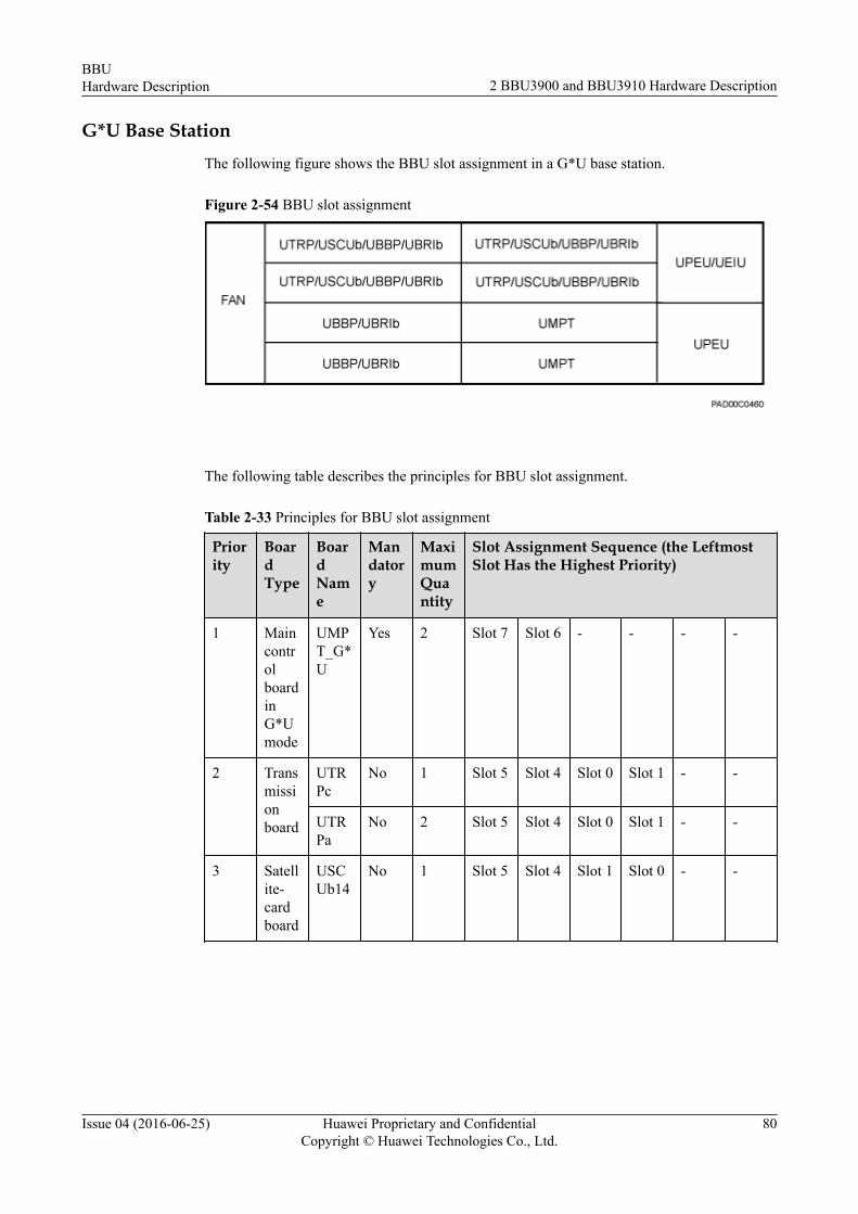
G*U Base StationThe following figure shows the BBU slot assignment in a G*U base station.
Figure 2-54 BBU slot assignment
The following table describes the principles for BBU slot assignment.
Table 2-33 Principles for BBU slot assignment
Priority
BoardType
BoardName
Mandatory
MaximumQuantity
Slot Assignment Sequence (the LeftmostSlot Has the Highest Priority)
1 MaincontrolboardinG*Umode
UMPT_G*U
Yes 2 Slot 7 Slot 6 - - - -
2 Transmissionboard
UTRPc
No 1 Slot 5 Slot 4 Slot 0 Slot 1 - -
UTRPa
No 2 Slot 5 Slot 4 Slot 0 Slot 1 - -
3 Satellite-cardboard
USCUb14
No 1 Slot 5 Slot 4 Slot 1 Slot 0 - -
BBUHardware Description 2 BBU3900 and BBU3910 Hardware Description
Issue 04 (2016-06-25) Huawei Proprietary and ConfidentialCopyright © Huawei Technologies Co., Ltd.
80

Priority
BoardType
BoardName
Mandatory
MaximumQuantity
Slot Assignment Sequence (the LeftmostSlot Has the Highest Priority)
4 Basebandprocessingboardinmultiplemodes
UBBP_G*U
No 2 Slot 3 Slot 2 Slot 1 Slot 0 Slot 4 Slot 5
5 BasebandprocessingboardinUMTSmode
UBBP_U
Yes 5 Slot 3 Slot 2 Slot 1 Slot 0 Slot 4 Slot 5
6 BasebandprocessingboardinGSMmode
UBBP_G
No 2 Slot 3 Slot 2 Slot 1 Slot 0 Slot 4 Slot 5
7 BasebandradiointerfaceboardinGSMmodeormultiplemodes
UBRIb
No 2 Slot 3 Slot 2 Slot 1 Slot 0 Slot 4 Slot 5
The following figure shows the typical configuration of BBU boards.
BBUHardware Description 2 BBU3900 and BBU3910 Hardware Description
Issue 04 (2016-06-25) Huawei Proprietary and ConfidentialCopyright © Huawei Technologies Co., Ltd.
81

Figure 2-55 Typical configuration of BBU boards
BBU Slot Assignment in GL and G*L Base StationsThis section describes the principles for BBU3910 slot assignment in GL and G*L basestations.
GL Base StationThe following figure shows the BBU slot assignment.
Figure 2-56 BBU slot assignment
The following table describes the principles for BBU slot assignment.
BBUHardware Description 2 BBU3900 and BBU3910 Hardware Description
Issue 04 (2016-06-25) Huawei Proprietary and ConfidentialCopyright © Huawei Technologies Co., Ltd.
82
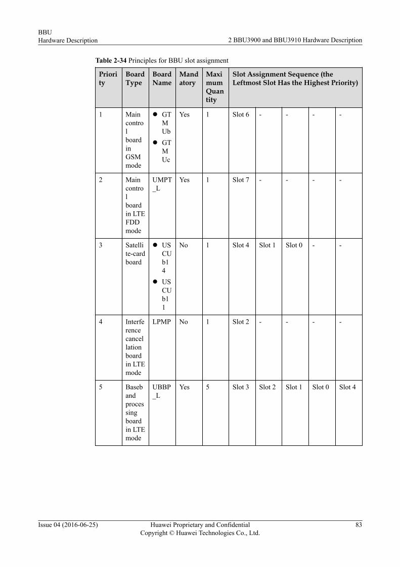
Table 2-34 Principles for BBU slot assignment
Priority
BoardType
BoardName
Mandatory
MaximumQuantity
Slot Assignment Sequence (theLeftmost Slot Has the Highest Priority)
1 MaincontrolboardinGSMmode
l GTMUb
l GTMUc
Yes 1 Slot 6 - - - -
2 Maincontrolboardin LTEFDDmode
UMPT_L
Yes 1 Slot 7 - - - -
3 Satellite-cardboard
l USCUb14
l USCUb11
No 1 Slot 4 Slot 1 Slot 0 - -
4 Interferencecancellationboardin LTEmode
LPMP No 1 Slot 2 - - - -
5 Basebandprocessingboardin LTEmode
UBBP_L
Yes 5 Slot 3 Slot 2 Slot 1 Slot 0 Slot 4
BBUHardware Description 2 BBU3900 and BBU3910 Hardware Description
Issue 04 (2016-06-25) Huawei Proprietary and ConfidentialCopyright © Huawei Technologies Co., Ltd.
83
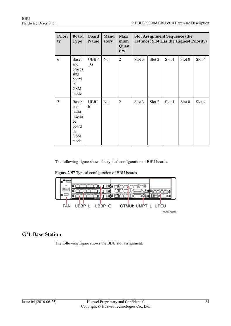
Priority
BoardType
BoardName
Mandatory
MaximumQuantity
Slot Assignment Sequence (theLeftmost Slot Has the Highest Priority)
6 BasebandprocessingboardinGSMmode
UBBP_G
No 2 Slot 3 Slot 2 Slot 1 Slot 0 Slot 4
7 BasebandradiointerfaceboardinGSMmode
UBRIb
No 2 Slot 3 Slot 2 Slot 1 Slot 0 Slot 4
The following figure shows the typical configuration of BBU boards.
Figure 2-57 Typical configuration of BBU boards
G*L Base StationThe following figure shows the BBU slot assignment.
BBUHardware Description 2 BBU3900 and BBU3910 Hardware Description
Issue 04 (2016-06-25) Huawei Proprietary and ConfidentialCopyright © Huawei Technologies Co., Ltd.
84
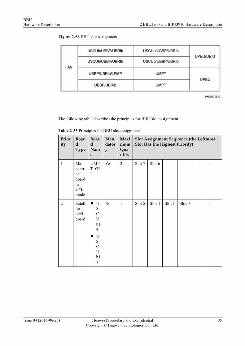
Figure 2-58 BBU slot assignment
The following table describes the principles for BBU slot assignment.
Table 2-35 Principles for BBU slot assignment
Priority
BoardType
BoardName
Mandatory
MaximumQuantity
Slot Assignment Sequence (the LeftmostSlot Has the Highest Priority)
1 MaincontrolboardinG*Lmode
UMPT_G*L
Yes 2 Slot 7 Slot 6 - - - -
2 Satellite-cardboard
l USCUb14
l USCUb11
No 1 Slot 5 Slot 4 Slot 1 Slot 0 - -
BBUHardware Description 2 BBU3900 and BBU3910 Hardware Description
Issue 04 (2016-06-25) Huawei Proprietary and ConfidentialCopyright © Huawei Technologies Co., Ltd.
85
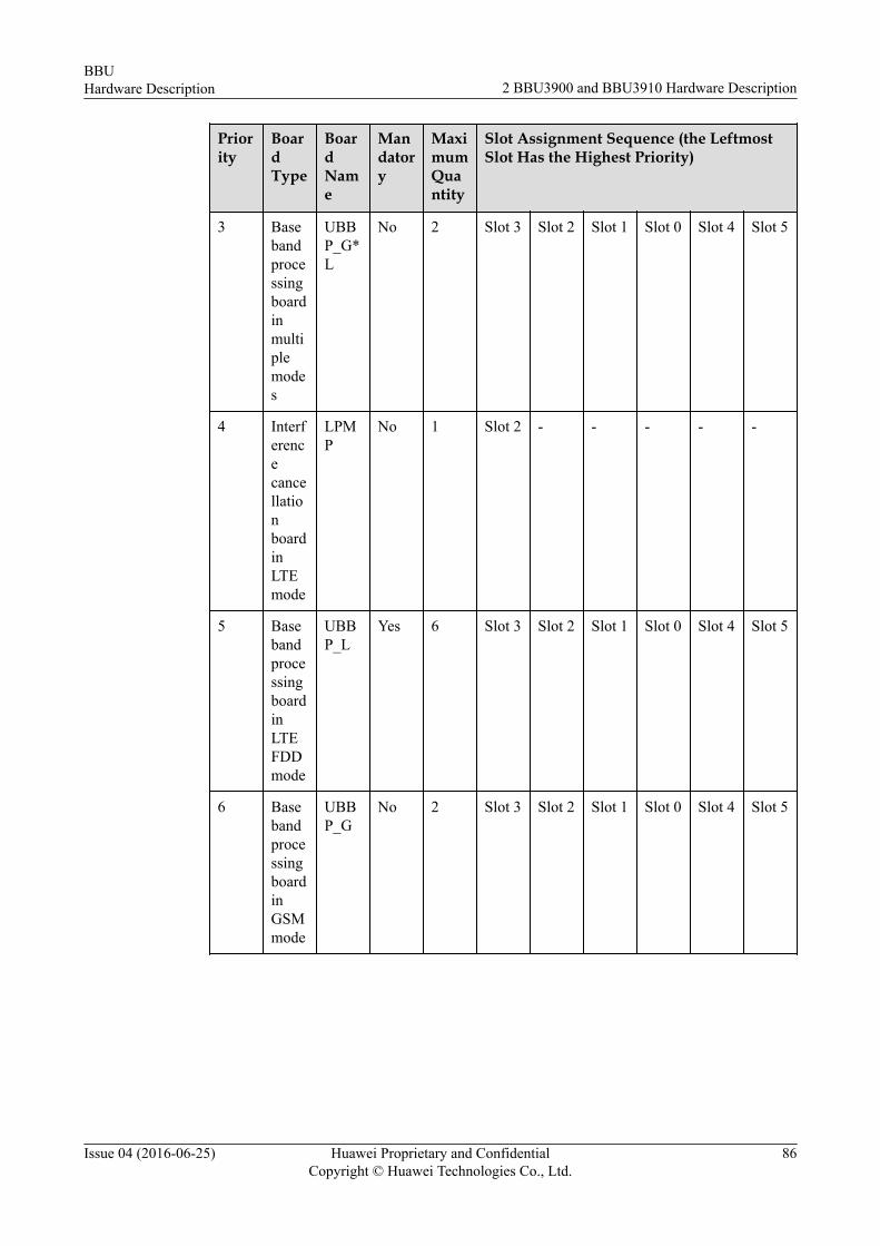
Priority
BoardType
BoardName
Mandatory
MaximumQuantity
Slot Assignment Sequence (the LeftmostSlot Has the Highest Priority)
3 Basebandprocessingboardinmultiplemodes
UBBP_G*L
No 2 Slot 3 Slot 2 Slot 1 Slot 0 Slot 4 Slot 5
4 InterferencecancellationboardinLTEmode
LPMP
No 1 Slot 2 - - - - -
5 BasebandprocessingboardinLTEFDDmode
UBBP_L
Yes 6 Slot 3 Slot 2 Slot 1 Slot 0 Slot 4 Slot 5
6 BasebandprocessingboardinGSMmode
UBBP_G
No 2 Slot 3 Slot 2 Slot 1 Slot 0 Slot 4 Slot 5
BBUHardware Description 2 BBU3900 and BBU3910 Hardware Description
Issue 04 (2016-06-25) Huawei Proprietary and ConfidentialCopyright © Huawei Technologies Co., Ltd.
86

Priority
BoardType
BoardName
Mandatory
MaximumQuantity
Slot Assignment Sequence (the LeftmostSlot Has the Highest Priority)
7 BasebandradiointerfaceboardinGSMmodeormultiplemodes
UBRIb
No 2 Slot 3 Slot 2 Slot 1 Slot 0 Slot 4 Slot 5
The following figure shows the typical configuration of BBU boards.
Figure 2-59 Typical configuration of BBU boards
BBU Slot Assignment in UL and U*L Base StationsThis section describes the principles for BBU3910 slot assignment in UL and U*L basestations.
UL Base StationThe following figure shows the BBU slot assignment.
BBUHardware Description 2 BBU3900 and BBU3910 Hardware Description
Issue 04 (2016-06-25) Huawei Proprietary and ConfidentialCopyright © Huawei Technologies Co., Ltd.
87

Figure 2-60 BBU slot assignment
The following table describes the principles for BBU slot assignment.
Table 2-36 Principles for BBU slot assignment
Priority
BoardType
BoardName
Mandatory
MaximumQuantity
Slot Assignment Sequence (the LeftmostSlot Has the Highest Priority)
1 MaincontrolboardinLTEFDDmode
UMPT_L
Yes 1 Slot 7 - - - - -
2 MaincontrolboardinUMTSmode
UMPT_U
Yes 1 Slot 6 - - - - -
3 TransmissionboardinUMTSmode
UTRPc
No 1 Slot 5 Slot 4 Slot 0 Slot 1 - -
UTRPa
No 2 Slot 5 Slot 4 Slot 0 Slot 1 - -
BBUHardware Description 2 BBU3900 and BBU3910 Hardware Description
Issue 04 (2016-06-25) Huawei Proprietary and ConfidentialCopyright © Huawei Technologies Co., Ltd.
88
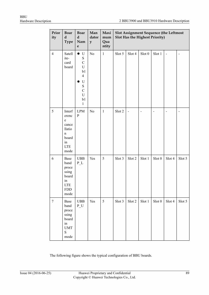
Priority
BoardType
BoardName
Mandatory
MaximumQuantity
Slot Assignment Sequence (the LeftmostSlot Has the Highest Priority)
4 Satellite-cardboard
l USCUb14
l USCUb11
No 1 Slot 5 Slot 4 Slot 0 Slot 1 - -
5 InterferencecancellationboardinLTEmode
LPMP
No 1 Slot 2 - - - - -
6 BasebandprocessingboardinLTEFDDmode
UBBP_L
Yes 5 Slot 3 Slot 2 Slot 1 Slot 0 Slot 4 Slot 5
7 BasebandprocessingboardinUMTSmode
UBBP_U
Yes 5 Slot 3 Slot 2 Slot 1 Slot 0 Slot 4 Slot 5
The following figure shows the typical configuration of BBU boards.
BBUHardware Description 2 BBU3900 and BBU3910 Hardware Description
Issue 04 (2016-06-25) Huawei Proprietary and ConfidentialCopyright © Huawei Technologies Co., Ltd.
89

Figure 2-61 Typical configuration of BBU boards
U*L Base Station
The following figure shows the BBU slot assignment.
Figure 2-62 BBU slot assignment
The following table describes the principles for BBU slot assignment.
Table 2-37 Principles for BBU slot assignment
Priority
BoardType
BoardName
Mandatory
MaximumQuantity
Slot Assignment Sequence (the LeftmostSlot Has the Highest Priority)
1 MaincontrolboardinU*Lmode
UMPT_U*L
Yes 2 Slot 7 Slot 6 - - - -
2 Transmissionboard
UTRPc
No 1 Slot 4 Slot 5 Slot 0 Slot 1 - -
BBUHardware Description 2 BBU3900 and BBU3910 Hardware Description
Issue 04 (2016-06-25) Huawei Proprietary and ConfidentialCopyright © Huawei Technologies Co., Ltd.
90

Priority
BoardType
BoardName
Mandatory
MaximumQuantity
Slot Assignment Sequence (the LeftmostSlot Has the Highest Priority)
3 Satellite-cardboard
l USCUb14
l USCUb11
No 1 Slot 5 Slot 4 Slot 1 Slot 0 - -
4 Basebandprocessingboardinmultiplemodes
UBBP_U*L
No 2 Slot 3 Slot 2 Slot 1 Slot 0 Slot 4 Slot 5
5 InterferencecancellationboardinLTEmode
LPMP
No 1 Slot 2 - - - - -
6 BasebandprocessingboardinLTEFDDmode
UBBP_L
Yes 5 Slot 3 Slot 2 Slot 1 Slot 0 Slot 4 Slot 5
BBUHardware Description 2 BBU3900 and BBU3910 Hardware Description
Issue 04 (2016-06-25) Huawei Proprietary and ConfidentialCopyright © Huawei Technologies Co., Ltd.
91

Priority
BoardType
BoardName
Mandatory
MaximumQuantity
Slot Assignment Sequence (the LeftmostSlot Has the Highest Priority)
7 BasebandprocessingboardinUMTSmode
UBBP_U
Yes 5 Slot 3 Slot 2 Slot 1 Slot 0 Slot 4 Slot 5
The following figure shows the typical configuration of BBU boards.
Figure 2-63 Typical configuration of BBU boards
U*L Base Station Using BBU Interconnection
In a scenario where two or more BBUs are connected to universal switching units (USUs)using interconnection signal cables, the principles for BBU slot assignment are different fromthose in a single BBU scenario. The following figure shows the principles for BBU slotassignment in a BBU interconnection scenario.
Figure 2-64 BBU slot assignment
BBUHardware Description 2 BBU3900 and BBU3910 Hardware Description
Issue 04 (2016-06-25) Huawei Proprietary and ConfidentialCopyright © Huawei Technologies Co., Ltd.
92
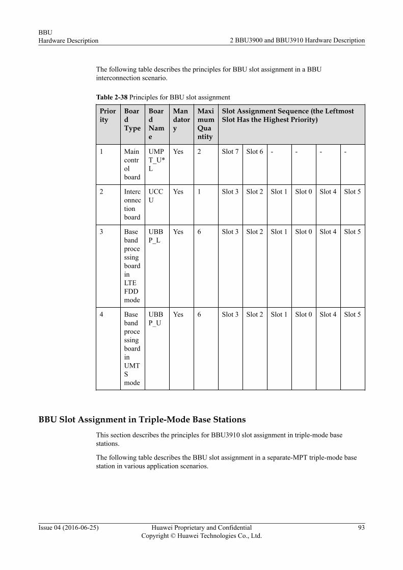
The following table describes the principles for BBU slot assignment in a BBUinterconnection scenario.
Table 2-38 Principles for BBU slot assignment
Priority
BoardType
BoardName
Mandatory
MaximumQuantity
Slot Assignment Sequence (the LeftmostSlot Has the Highest Priority)
1 Maincontrolboard
UMPT_U*L
Yes 2 Slot 7 Slot 6 - - - -
2 Interconnectionboard
UCCU
Yes 1 Slot 3 Slot 2 Slot 1 Slot 0 Slot 4 Slot 5
3 BasebandprocessingboardinLTEFDDmode
UBBP_L
Yes 6 Slot 3 Slot 2 Slot 1 Slot 0 Slot 4 Slot 5
4 BasebandprocessingboardinUMTSmode
UBBP_U
Yes 6 Slot 3 Slot 2 Slot 1 Slot 0 Slot 4 Slot 5
BBU Slot Assignment in Triple-Mode Base StationsThis section describes the principles for BBU3910 slot assignment in triple-mode basestations.
The following table describes the BBU slot assignment in a separate-MPT triple-mode basestation in various application scenarios.
BBUHardware Description 2 BBU3900 and BBU3910 Hardware Description
Issue 04 (2016-06-25) Huawei Proprietary and ConfidentialCopyright © Huawei Technologies Co., Ltd.
93
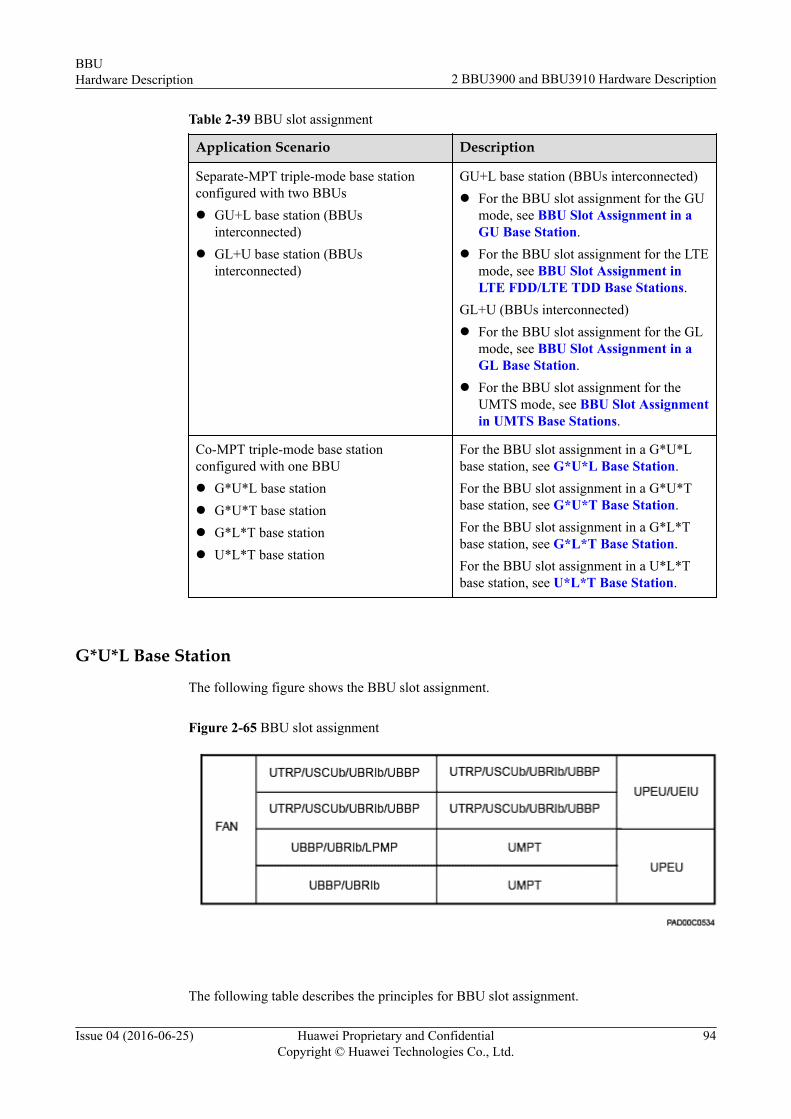
Table 2-39 BBU slot assignment
Application Scenario Description
Separate-MPT triple-mode base stationconfigured with two BBUsl GU+L base station (BBUs
interconnected)l GL+U base station (BBUs
interconnected)
GU+L base station (BBUs interconnected)l For the BBU slot assignment for the GU
mode, see BBU Slot Assignment in aGU Base Station.
l For the BBU slot assignment for the LTEmode, see BBU Slot Assignment inLTE FDD/LTE TDD Base Stations.
GL+U (BBUs interconnected)l For the BBU slot assignment for the GL
mode, see BBU Slot Assignment in aGL Base Station.
l For the BBU slot assignment for theUMTS mode, see BBU Slot Assignmentin UMTS Base Stations.
Co-MPT triple-mode base stationconfigured with one BBUl G*U*L base stationl G*U*T base stationl G*L*T base stationl U*L*T base station
For the BBU slot assignment in a G*U*Lbase station, see G*U*L Base Station.For the BBU slot assignment in a G*U*Tbase station, see G*U*T Base Station.For the BBU slot assignment in a G*L*Tbase station, see G*L*T Base Station.For the BBU slot assignment in a U*L*Tbase station, see U*L*T Base Station.
G*U*L Base Station
The following figure shows the BBU slot assignment.
Figure 2-65 BBU slot assignment
The following table describes the principles for BBU slot assignment.
BBUHardware Description 2 BBU3900 and BBU3910 Hardware Description
Issue 04 (2016-06-25) Huawei Proprietary and ConfidentialCopyright © Huawei Technologies Co., Ltd.
94
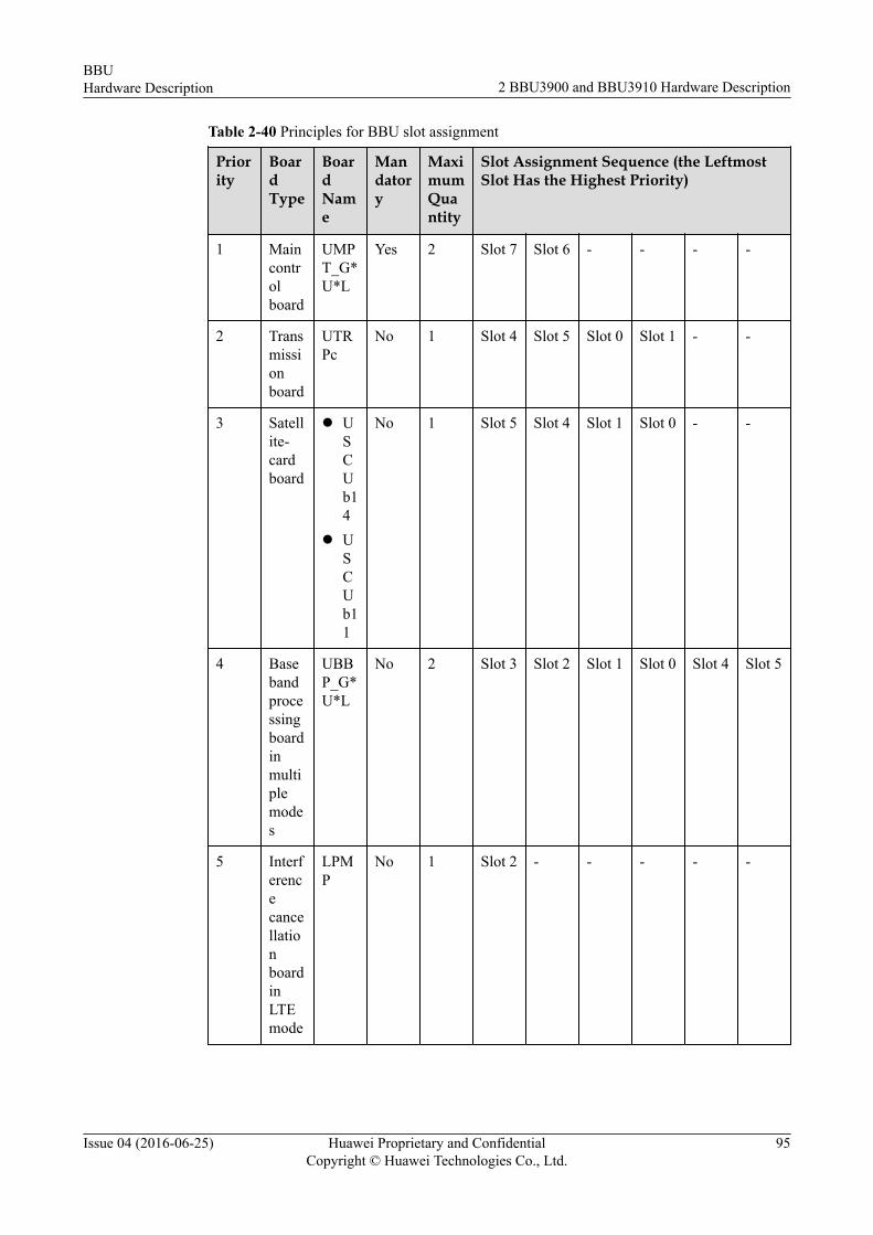
Table 2-40 Principles for BBU slot assignment
Priority
BoardType
BoardName
Mandatory
MaximumQuantity
Slot Assignment Sequence (the LeftmostSlot Has the Highest Priority)
1 Maincontrolboard
UMPT_G*U*L
Yes 2 Slot 7 Slot 6 - - - -
2 Transmissionboard
UTRPc
No 1 Slot 4 Slot 5 Slot 0 Slot 1 - -
3 Satellite-cardboard
l USCUb14
l USCUb11
No 1 Slot 5 Slot 4 Slot 1 Slot 0 - -
4 Basebandprocessingboardinmultiplemodes
UBBP_G*U*L
No 2 Slot 3 Slot 2 Slot 1 Slot 0 Slot 4 Slot 5
5 InterferencecancellationboardinLTEmode
LPMP
No 1 Slot 2 - - - - -
BBUHardware Description 2 BBU3900 and BBU3910 Hardware Description
Issue 04 (2016-06-25) Huawei Proprietary and ConfidentialCopyright © Huawei Technologies Co., Ltd.
95
Priority
BoardType
BoardName
Mandatory
MaximumQuantity
Slot Assignment Sequence (the LeftmostSlot Has the Highest Priority)
6 BasebandprocessingboardinLTEFDDmode
UBBP_L
Yes 6 Slot 3 Slot 2 Slot 1 Slot 0 Slot 4 Slot 5
7 BasebandprocessingboardinUMTSmode
UBBP_U
Yes 6 Slot 3 Slot 2 Slot 1 Slot 0 Slot 4 Slot 5
8 BasebandprocessingboardinGSMmode
UBBP_G
No 2 Slot 3 Slot 2 Slot 1 Slot 0 Slot 4 Slot 5
9 BasebandradiointerfaceboardinGSMmodeormultiplemodes
UBRIb
No 2 Slot 3 Slot 2 Slot 1 Slot 0 Slot 4 Slot 5
The following figure shows the typical configuration of BBU boards.
BBUHardware Description 2 BBU3900 and BBU3910 Hardware Description
Issue 04 (2016-06-25) Huawei Proprietary and ConfidentialCopyright © Huawei Technologies Co., Ltd.
96

Figure 2-66 Typical configuration of BBU boards
G*U*T Base Station
The following figure shows the BBU slot assignment.
Figure 2-67 BBU slot assignment
The following table describes the principles for BBU slot assignment.
Table 2-41 Principles for BBU slot assignment
Priority
BoardType
BoardName
Mandatory
MaximumQuantity
Slot Assignment Sequence (the LeftmostSlot Has the Highest Priority)
1 Maincontrolboard
UMPT_G*U*T
Yes 2 Slot 7 Slot 6 - - - -
2 Transmissionboard
UTRPc
No 1 Slot 4 Slot 5 Slot 0 Slot 1 - -
BBUHardware Description 2 BBU3900 and BBU3910 Hardware Description
Issue 04 (2016-06-25) Huawei Proprietary and ConfidentialCopyright © Huawei Technologies Co., Ltd.
97

Priority
BoardType
BoardName
Mandatory
MaximumQuantity
Slot Assignment Sequence (the LeftmostSlot Has the Highest Priority)
3 Satellite-cardboard
l USCUb14
l USCUb11
No 1 Slot 5 Slot 4 Slot 1 Slot 0 - -
4 BasebandprocessingboardinLTETDDmode
UBBP_T
Yes 6 Slot 3 Slot 2 Slot 1 Slot 0 Slot 4 Slot 5
5 BasebandprocessingboardinUMTSmode
UBBP_U
Yes 6 Slot 3 Slot 2 Slot 1 Slot 0 Slot 4 Slot 5
6 BasebandprocessingboardinGSMmode
UBBP_G
No 2 Slot 3 Slot 2 Slot 1 Slot 0 Slot 4 Slot 5
BBUHardware Description 2 BBU3900 and BBU3910 Hardware Description
Issue 04 (2016-06-25) Huawei Proprietary and ConfidentialCopyright © Huawei Technologies Co., Ltd.
98
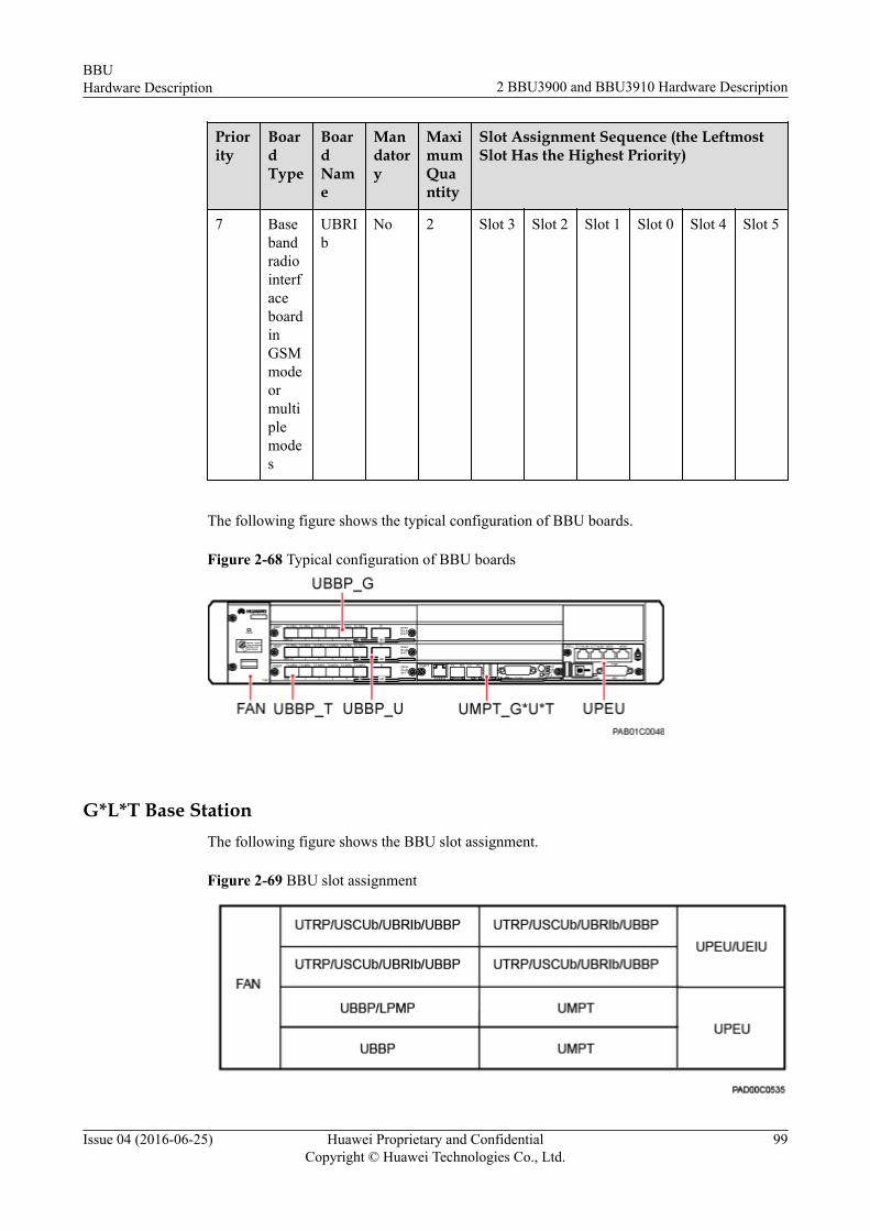
Priority
BoardType
BoardName
Mandatory
MaximumQuantity
Slot Assignment Sequence (the LeftmostSlot Has the Highest Priority)
7 BasebandradiointerfaceboardinGSMmodeormultiplemodes
UBRIb
No 2 Slot 3 Slot 2 Slot 1 Slot 0 Slot 4 Slot 5
The following figure shows the typical configuration of BBU boards.
Figure 2-68 Typical configuration of BBU boards
G*L*T Base StationThe following figure shows the BBU slot assignment.
Figure 2-69 BBU slot assignment
BBUHardware Description 2 BBU3900 and BBU3910 Hardware Description
Issue 04 (2016-06-25) Huawei Proprietary and ConfidentialCopyright © Huawei Technologies Co., Ltd.
99
The following table describes the principles for BBU slot assignment.
Table 2-42 Principles for BBU slot assignment
Priority
BoardType
BoardName
Mandatory
MaximumQuantity
Slot Assignment Sequence (the LeftmostSlot Has the Highest Priority)
1 Maincontrolboard
UMPT_G*L*T
Yes 2 Slot 7 Slot 6 - - - -
2 Transmissionboard
UTRPc
No 1 Slot 4 Slot 5 Slot 0 Slot 1 - -
3 Satellite-cardboard
l USCUb14
l USCUb11
No 1 Slot 5 Slot 4 Slot 1 Slot 0 - -
4 InterferencecancellationboardinLTEmode
LPMP
No 1 Slot 2 - - - - -
5 BasebandprocessingboardinLTEFDDmode
UBBP_L
Yes 6 Slot 3 Slot 2 Slot 1 Slot 0 Slot 4 Slot 5
BBUHardware Description 2 BBU3900 and BBU3910 Hardware Description
Issue 04 (2016-06-25) Huawei Proprietary and ConfidentialCopyright © Huawei Technologies Co., Ltd.
100

Priority
BoardType
BoardName
Mandatory
MaximumQuantity
Slot Assignment Sequence (the LeftmostSlot Has the Highest Priority)
6 BasebandprocessingboardinLTETDDmode
UBBP_T
Yes 6 Slot 3 Slot 2 Slot 1 Slot 0 Slot 4 Slot 5
7 BasebandprocessingboardinGSMmode
UBBP_G
No 2 Slot 3 Slot 2 Slot 1 Slot 0 Slot 4 Slot 5
8 BasebandradiointerfaceboardinGSMmodeormultiplemodes
UBRIb
No 2 Slot 3 Slot 2 Slot 1 Slot 0 Slot 4 Slot 5
The following figure shows the typical configuration of BBU boards.
Figure 2-70 Typical configuration of BBU boards
BBUHardware Description 2 BBU3900 and BBU3910 Hardware Description
Issue 04 (2016-06-25) Huawei Proprietary and ConfidentialCopyright © Huawei Technologies Co., Ltd.
101
U*L*T Base Station
The following figure shows the BBU slot assignment.
Figure 2-71 BBU slot assignment
The following table describes the principles for BBU slot assignment.
Table 2-43 Principles for BBU slot assignment
Priority
BoardType
BoardName
Mandatory
MaximumQuantity
Slot Assignment Sequence (the LeftmostSlot Has the Highest Priority)
1 Maincontrolboard
UMPT_U*L*T
Yes 2 Slot 7 Slot 6 - - - -
2 Transmissionboard
UTRPc
No 1 Slot 4 Slot 5 Slot 0 Slot 1 - -
3 Satellite-cardboard
l USCUb14
l USCUb11
No 1 Slot 5 Slot 4 Slot 1 Slot 0 - -
BBUHardware Description 2 BBU3900 and BBU3910 Hardware Description
Issue 04 (2016-06-25) Huawei Proprietary and ConfidentialCopyright © Huawei Technologies Co., Ltd.
102

Priority
BoardType
BoardName
Mandatory
MaximumQuantity
Slot Assignment Sequence (the LeftmostSlot Has the Highest Priority)
4 InterferencecancellationboardinLTEmode
LPMP
No 1 Slot 2 - - - - -
5 BasebandprocessingboardinLTEFDDmode
UBBP_L
Yes 6 Slot 3 Slot 2 Slot 1 Slot 0 Slot 4 Slot 5
6 BasebandprocessingboardinLTETDDmode
UBBP_T
Yes 6 Slot 3 Slot 2 Slot 1 Slot 0 Slot 4 Slot 5
7 BasebandprocessingboardinUMTSmode
UBBP_U
Yes 6 Slot 3 Slot 2 Slot 1 Slot 0 Slot 4 Slot 5
The following figure shows the typical configuration of BBU boards.
BBUHardware Description 2 BBU3900 and BBU3910 Hardware Description
Issue 04 (2016-06-25) Huawei Proprietary and ConfidentialCopyright © Huawei Technologies Co., Ltd.
103

Figure 2-72 Typical configuration of BBU boards
BBU Slot Assignment in Quadruple-Mode Base Stations
This section describes the principles for BBU3910 slot assignment in quadruple-mode basestations.
The following table describes the BBU slot assignment in quadruple-mode base stations.
Table 2-44 BBU slot assignment
Application Scenario Description
Co-MPT quadruple-mode base stationconfigured with oneBBU: G*U*L*T basestation
The following table describes the principles for BBU slotassignment in a G*U*L*T base station.
The following figure shows the BBU slot assignment in a G*U*L*T base station.
Figure 2-73 BBU slot assignment
The following table describes the principles for BBU slot assignment.
BBUHardware Description 2 BBU3900 and BBU3910 Hardware Description
Issue 04 (2016-06-25) Huawei Proprietary and ConfidentialCopyright © Huawei Technologies Co., Ltd.
104
Table 2-45 Principles for BBU slot assignment
Priority
BoardType
BoardName
Mandatory
MaximumQuantity
Slot Assignment Sequence (the LeftmostSlot Has the Highest Priority)
1 Maincontrolboard
UMPT_G*U*L*T
Yes 2 Slot 7 Slot 6 - - - -
2 Transmissionboard
UTRPc
No 1 Slot 5 Slot 4 Slot 0 Slot 1 - -
UTRPa
No 2 Slot 5 Slot 4 Slot 0 Slot 1 - -
3 Satellite-cardboard
l USCUb14
l USCUb11
No 1 Slot 5 Slot 4 Slot 1 Slot 0 - -
4 Basebandprocessingboardinmultiplemodes
UBBP_G*U*L*T
No 2 Slot 3 Slot 2 - - - -
5 InterferencecancellationboardinLTEmode
LPMP
No 1 Slot 2 - - - - -
BBUHardware Description 2 BBU3900 and BBU3910 Hardware Description
Issue 04 (2016-06-25) Huawei Proprietary and ConfidentialCopyright © Huawei Technologies Co., Ltd.
105

Priority
BoardType
BoardName
Mandatory
MaximumQuantity
Slot Assignment Sequence (the LeftmostSlot Has the Highest Priority)
6 BasebandprocessingboardinLTEFDDmode
UBBP_L
Yes 6 Slot 3 Slot 2 Slot 1 Slot 0 Slot 4 Slot 5
7 BasebandprocessingboardinLTETDDmode
UBBP_T
Yes 6 Slot 3 Slot 2 Slot 1 Slot 0 Slot 4 Slot 5
8 BasebandprocessingboardinUMTSmode
UBBP_U
Yes 6 Slot 3 Slot 2 Slot 1 Slot 0 Slot 4 Slot 5
9 BasebandprocessingboardinGSMmode
UBBP_G
No 2 Slot 3 Slot 2 Slot 1 Slot 0 Slot 4 Slot 5
10 BasebandradiointerfaceboardinGSMmode
UBRIb
No 2 Slot 3 Slot 2 Slot 1 Slot 0 Slot 4 Slot 5
BBUHardware Description 2 BBU3900 and BBU3910 Hardware Description
Issue 04 (2016-06-25) Huawei Proprietary and ConfidentialCopyright © Huawei Technologies Co., Ltd.
106
The following figure shows the typical configuration of BBU boards.
Figure 2-74 Typical configuration of BBU boards
2.5 BBU3900 and BBU3910 BoardsA BBU includes the following boards: main processing board, baseband processing board,transmission extension board, fan module, power module, monitoring module, clock boardwith a satellite card, baseband extension board, and infrastructure interconnection board.
2.5.1 UMPTA UMPT is a universal main processing and transmission unit and can be installed in aBBU3900 or BBU3910.
The following figures show a UMPT panel.
NOTE
On the lower left corner of a board, there is a silkscreen indicating its type.
Figure 2-75 UMPTa/UMPTb panel
BBUHardware Description 2 BBU3900 and BBU3910 Hardware Description
Issue 04 (2016-06-25) Huawei Proprietary and ConfidentialCopyright © Huawei Technologies Co., Ltd.
107
Figure 2-76 UMPTe panel
SpecificationsNOTE
A license is required to support board specifications.
The following table lists the transmission port specifications of UMPT boards.
Table 2-46 Transmission port specifications of UMPT boards
Board Name/Satellite CardSupported
ApplicableMode
TransmissionMode
Quantityof Ports
PortCapacity
Full/Half-Duplex
l UMPTa1(without asatellite card)
l UMPTa2(without asatellite card)
l GSM singlemode
l UMTS singlemode
l LTE FDDsingle mode
l Co-MPTmultiplemodes(includingany mode)
ATM overE1/T1a orIP overE1/T1
1 Fourchannels
-
Transmission overFE/GEelectricalports
1 10 Mbit/s,100Mbit/s, or1000Mbit/s
Full- orhalf-duplex
Transmission overFE/GEopticalports
1 100 Mbit/sor 1000Mbit/s
Full-duplex
l UMPTb1(without asatellite card)
l UMPTb2(with a GPSsatellite card)
l GSM singlemode
l UMTS singlemode
l LTE FDDsingle mode
l LTE TDDsingle mode
ATM overE1/T1a orIP overE1/T1
1 Fourchannels
-
Transmission overFE/GEelectricalports
1 10 Mbit/s,100Mbit/s, or1000Mbit/s
Full- orhalf-duplex
BBUHardware Description 2 BBU3900 and BBU3910 Hardware Description
Issue 04 (2016-06-25) Huawei Proprietary and ConfidentialCopyright © Huawei Technologies Co., Ltd.
108

Board Name/Satellite CardSupported
ApplicableMode
TransmissionMode
Quantityof Ports
PortCapacity
Full/Half-Duplex
l Co-MPTmultiplemodes(includingany mode)
Transmission overFE/GEopticalports
1 100 Mbit/sor 1000Mbit/s
Full-duplex
UMPTa6 (with aGPS satellitecard)
l LTE FDDsingle mode
l LTE TDDsingle mode
IP overE1/T1
1 Fourchannels
-
Transmission overFE/GEelectricalports
1 10 Mbit/s,100Mbit/s, or1000Mbit/s
Full- orhalf-duplex
Transmission overFE/GEopticalports
1 100 Mbit/sor 1000Mbit/s
Full-duplex
l UMPTe1(without asatellite card)
l UMPTe2(with a GPSsatellite card)
l GSM singlemode
l UMTS singlemode
l LTE FDDsingle mode
l LTE TDDsingle mode
l Co-MPTmultiplemodes(includingany mode)
Transmission overFE/GEelectricalports
2 10 Mbit/s,100Mbit/s, or1000Mbit/s
Full- orhalf-duplex
Transmission overFE/GE/10GEopticalports
2 1000Mbit/s or10,000Mbit/s
Full-duplex
a: ATM over E1/T1 is supported only in UMTS mode.
The following table lists the carrier specifications of a UMPT working in GSM mode.
BBUHardware Description 2 BBU3900 and BBU3910 Hardware Description
Issue 04 (2016-06-25) Huawei Proprietary and ConfidentialCopyright © Huawei Technologies Co., Ltd.
109

Table 2-47 Carrier specifications of UMPT boards
Board Applicable Mode TransmissionMode
MaximumNumber ofSupportedCarriers
UMPTb1 orUMPTb2
GSM IP over E1/T1 or IPover FE/GE
72
UMPTe GSM IP over FE/GE 72
NOTE
If a UMPTa1, UMPTa2, UMPTb1, or UMPTb2 works in UMTS mode, the signaling specifications of theUMPTa1, UMPTa2, UMPTb1, or UMPTb2 depends on the configured baseband processing board. Fordetails, see section "Technical Specifications of the BBU3900s and BBU3910s" in 3900 Series Base StationTechnical Description.
The following table lists the signaling specifications of UMPT boards working in LTE FDDmode.
Table 2-48 Signaling specifications
Board Signaling Specifications (BHCA)a
UMPTa1/UMPTa2/UMPTa6 288000
UMPTb1/UMPTb2 360000
UMPTe1/UMPTe2 1620000
a: The BHCA specifications are based on the smart device traffic model.
NOTE
For details about the datacard traffic model and smart device traffic model, see section "TechnicalSpecifications of the eNodeB FDD" in 3900 Series Base Station Technical Description.
The following table lists the maximum number of UEs in RRC connected mode supported byUMPT boards working in LTE FDD mode.
BBUHardware Description 2 BBU3900 and BBU3910 Hardware Description
Issue 04 (2016-06-25) Huawei Proprietary and ConfidentialCopyright © Huawei Technologies Co., Ltd.
110
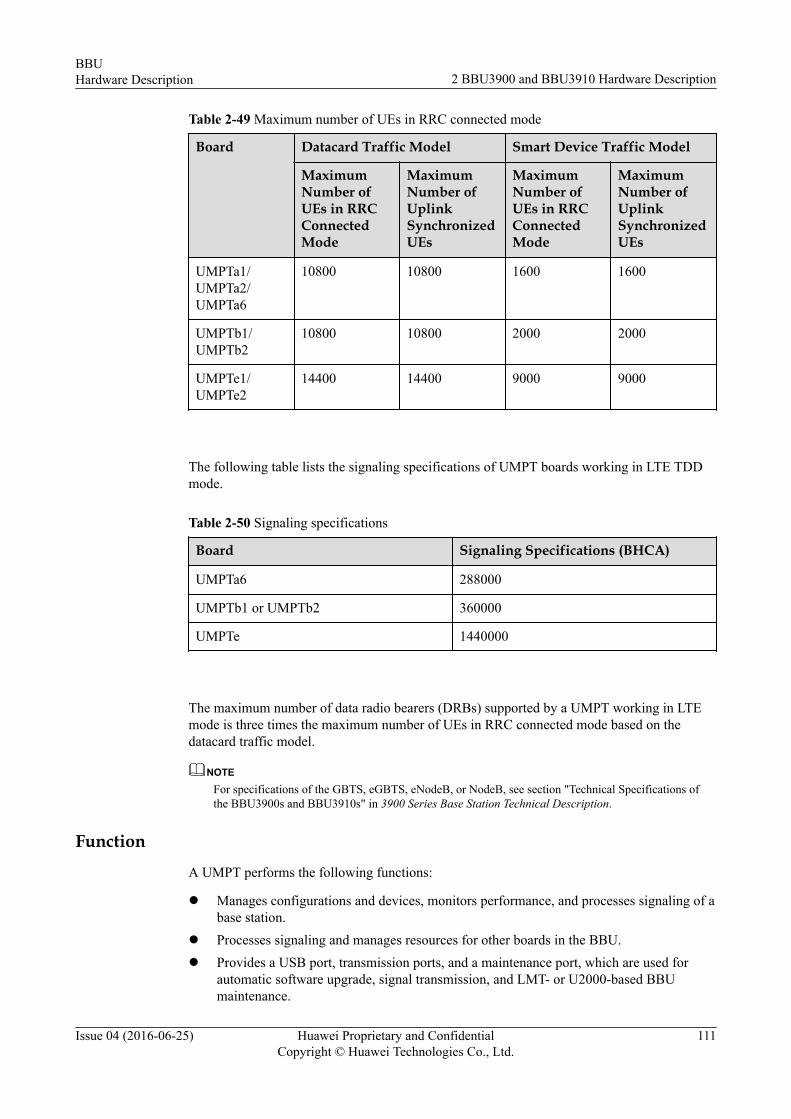
Table 2-49 Maximum number of UEs in RRC connected mode
Board Datacard Traffic Model Smart Device Traffic Model
MaximumNumber ofUEs in RRCConnectedMode
MaximumNumber ofUplinkSynchronizedUEs
MaximumNumber ofUEs in RRCConnectedMode
MaximumNumber ofUplinkSynchronizedUEs
UMPTa1/UMPTa2/UMPTa6
10800 10800 1600 1600
UMPTb1/UMPTb2
10800 10800 2000 2000
UMPTe1/UMPTe2
14400 14400 9000 9000
The following table lists the signaling specifications of UMPT boards working in LTE TDDmode.
Table 2-50 Signaling specifications
Board Signaling Specifications (BHCA)
UMPTa6 288000
UMPTb1 or UMPTb2 360000
UMPTe 1440000
The maximum number of data radio bearers (DRBs) supported by a UMPT working in LTEmode is three times the maximum number of UEs in RRC connected mode based on thedatacard traffic model.
NOTEFor specifications of the GBTS, eGBTS, eNodeB, or NodeB, see section "Technical Specifications ofthe BBU3900s and BBU3910s" in 3900 Series Base Station Technical Description.
Function
A UMPT performs the following functions:
l Manages configurations and devices, monitors performance, and processes signaling of abase station.
l Processes signaling and manages resources for other boards in the BBU.l Provides a USB port, transmission ports, and a maintenance port, which are used for
automatic software upgrade, signal transmission, and LMT- or U2000-based BBUmaintenance.
BBUHardware Description 2 BBU3900 and BBU3910 Hardware Description
Issue 04 (2016-06-25) Huawei Proprietary and ConfidentialCopyright © Huawei Technologies Co., Ltd.
111
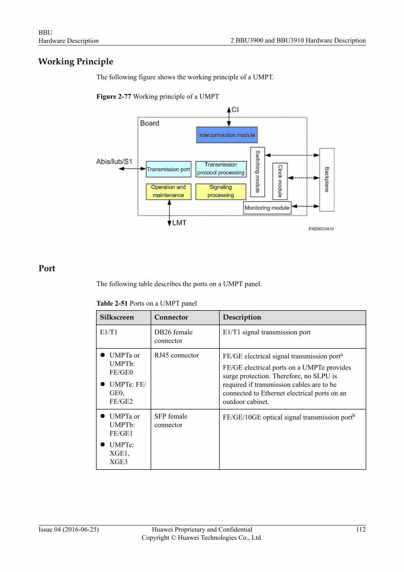
Working PrincipleThe following figure shows the working principle of a UMPT.
Figure 2-77 Working principle of a UMPT
PortThe following table describes the ports on a UMPT panel.
Table 2-51 Ports on a UMPT panel
Silkscreen Connector Description
E1/T1 DB26 femaleconnector
E1/T1 signal transmission port
l UMPTa orUMPTb:FE/GE0
l UMPTe: FE/GE0,FE/GE2
RJ45 connector FE/GE electrical signal transmission porta
FE/GE electrical ports on a UMPTe providessurge protection. Therefore, no SLPU isrequired if transmission cables are to beconnected to Ethernet electrical ports on anoutdoor cabinet.
l UMPTa orUMPTb:FE/GE1
l UMPTe:XGE1,XGE3
SFP femaleconnector
FE/GE/10GE optical signal transmission portb
BBUHardware Description 2 BBU3900 and BBU3910 Hardware Description
Issue 04 (2016-06-25) Huawei Proprietary and ConfidentialCopyright © Huawei Technologies Co., Ltd.
112
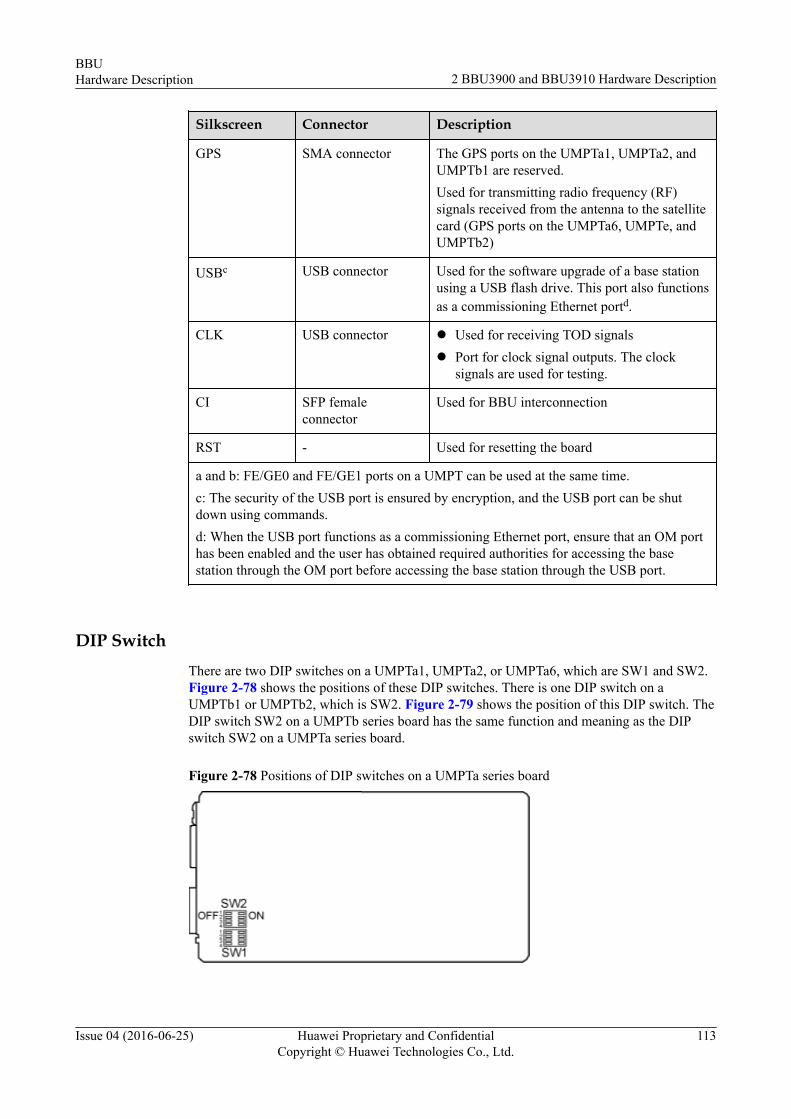
Silkscreen Connector Description
GPS SMA connector The GPS ports on the UMPTa1, UMPTa2, andUMPTb1 are reserved.Used for transmitting radio frequency (RF)signals received from the antenna to the satellitecard (GPS ports on the UMPTa6, UMPTe, andUMPTb2)
USBc USB connector Used for the software upgrade of a base stationusing a USB flash drive. This port also functionsas a commissioning Ethernet portd.
CLK USB connector l Used for receiving TOD signalsl Port for clock signal outputs. The clock
signals are used for testing.
CI SFP femaleconnector
Used for BBU interconnection
RST - Used for resetting the board
a and b: FE/GE0 and FE/GE1 ports on a UMPT can be used at the same time.c: The security of the USB port is ensured by encryption, and the USB port can be shutdown using commands.d: When the USB port functions as a commissioning Ethernet port, ensure that an OM porthas been enabled and the user has obtained required authorities for accessing the basestation through the OM port before accessing the base station through the USB port.
DIP SwitchThere are two DIP switches on a UMPTa1, UMPTa2, or UMPTa6, which are SW1 and SW2.Figure 2-78 shows the positions of these DIP switches. There is one DIP switch on aUMPTb1 or UMPTb2, which is SW2. Figure 2-79 shows the position of this DIP switch. TheDIP switch SW2 on a UMPTb series board has the same function and meaning as the DIPswitch SW2 on a UMPTa series board.
Figure 2-78 Positions of DIP switches on a UMPTa series board
BBUHardware Description 2 BBU3900 and BBU3910 Hardware Description
Issue 04 (2016-06-25) Huawei Proprietary and ConfidentialCopyright © Huawei Technologies Co., Ltd.
113
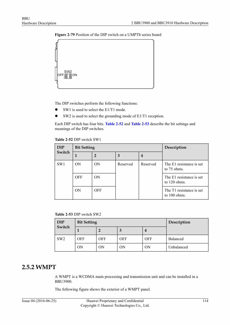
Figure 2-79 Position of the DIP switch on a UMPTb series board
The DIP switches perform the following functions:l SW1 is used to select the E1/T1 mode.l SW2 is used to select the grounding mode of E1/T1 reception.
Each DIP switch has four bits. Table 2-52 and Table 2-53 describe the bit settings andmeanings of the DIP switches.
Table 2-52 DIP switch SW1
DIPSwitch
Bit Setting Description
1 2 3 4
SW1 ON ON Reserved Reserved The E1 resistance is setto 75 ohms.
OFF ON The E1 resistance is setto 120 ohms.
ON OFF The T1 resistance is setto 100 ohms.
Table 2-53 DIP switch SW2
DIPSwitch
Bit Setting Description
1 2 3 4
SW2 OFF OFF OFF OFF Balanced
ON ON ON ON Unbalanced
2.5.2 WMPTA WMPT is a WCDMA main processing and transmission unit and can be installed in aBBU3900.
The following figure shows the exterior of a WMPT panel.
BBUHardware Description 2 BBU3900 and BBU3910 Hardware Description
Issue 04 (2016-06-25) Huawei Proprietary and ConfidentialCopyright © Huawei Technologies Co., Ltd.
114

Figure 2-80 Exterior of a WMPT panel
Specifications
The following table lists the transmission port specifications of a WMPT.
Table 2-54 Transmission port specifications of a WMPT
Board ApplicableMode
Transmission Mode
Quantityof Ports
PortCapacity
Full/Half-Duplex
WMPT UMTS ATM overE1/T1 or IPover E1/T1
1 Fourchannels
Full-duplex
Transmission over FEoptical ports
1 10 Mbit/s or100 Mbit/s
Full-duplex
Transmission over FEelectricalports
1 10 Mbit/s or100 Mbit/s
Full-duplex
NOTEFor combined signaling specifications of a WMPT, see section "Technical Specifications of theBBU3900s and BBU3910s" in 3900 Series Base Station Technical Description.
Function
A WMPT performs the following functions:
l Manages configurations and devices, monitors performance, and processes signaling of abase station.
l Processes signaling and manages resources for other boards in the BBU.
l Provides a USB port, transmission ports, and a maintenance port, which are used forautomatic software upgrade, signal transmission, and LMT- or U2000-based BBUmaintenance.
Working Principle
The following figure shows the working principle of a WMPT.
BBUHardware Description 2 BBU3900 and BBU3910 Hardware Description
Issue 04 (2016-06-25) Huawei Proprietary and ConfidentialCopyright © Huawei Technologies Co., Ltd.
115
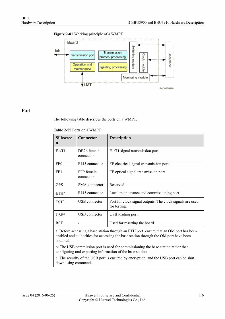
Figure 2-81 Working principle of a WMPT
PortThe following table describes the ports on a WMPT.
Table 2-55 Ports on a WMPT
Silkscreen
Connector Description
E1/T1 DB26 femaleconnector
E1/T1 signal transmission port
FE0 RJ45 connector FE electrical signal transmission port
FE1 SFP femaleconnector
FE optical signal transmission port
GPS SMA connector Reserved
ETHa RJ45 connector Local maintenance and commissioning port
TSTb USB connector Port for clock signal outputs. The clock signals are usedfor testing.
USBc USB connector USB loading port
RST - Used for resetting the board
a: Before accessing a base station through an ETH port, ensure that an OM port has beenenabled and authorities for accessing the base station through the OM port have beenobtained.b: The USB commission port is used for commissioning the base station rather thanconfiguring and exporting information of the base station.c: The security of the USB port is ensured by encryption, and the USB port can be shutdown using commands.
BBUHardware Description 2 BBU3900 and BBU3910 Hardware Description
Issue 04 (2016-06-25) Huawei Proprietary and ConfidentialCopyright © Huawei Technologies Co., Ltd.
116
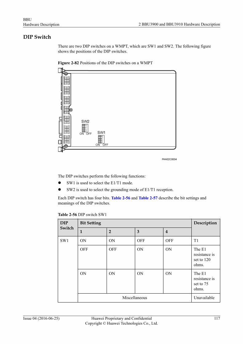
DIP SwitchThere are two DIP switches on a WMPT, which are SW1 and SW2. The following figureshows the positions of the DIP switches.
Figure 2-82 Positions of the DIP switches on a WMPT
The DIP switches perform the following functions:l SW1 is used to select the E1/T1 mode.l SW2 is used to select the grounding mode of E1/T1 reception.
Each DIP switch has four bits. Table 2-56 and Table 2-57 describe the bit settings andmeanings of the DIP switches.
Table 2-56 DIP switch SW1
DIPSwitch
Bit Setting Description
1 2 3 4
SW1 ON ON OFF OFF T1
OFF OFF ON ON The E1resistance isset to 120ohms.
ON ON ON ON The E1resistance isset to 75ohms.
Miscellaneous Unavailable
BBUHardware Description 2 BBU3900 and BBU3910 Hardware Description
Issue 04 (2016-06-25) Huawei Proprietary and ConfidentialCopyright © Huawei Technologies Co., Ltd.
117

Table 2-57 DIP switch SW2
DIPSwitch
Bit Setting Description
1 2 3 4
SW2 OFF OFF OFF OFF Balanced
ON ON ON ON Unbalanced
Miscellaneous Unavailable
2.5.3 GTMUA GTMU is a GSM transmission and timing and management unit. A GTMU can be installedin a BBU3900, and a GTMUb or GTMUc can be installed in a BBU3900 or BBU3910.
Figure 2-83, Figure 2-84, and Figure 2-85 show a GTMU panel, a GTMUb panel, and aGTMUc panel, respectively.
Figure 2-83 GTMU panel
Figure 2-84 GTMUb panel
Figure 2-85 GTMUc panel
BBUHardware Description 2 BBU3900 and BBU3910 Hardware Description
Issue 04 (2016-06-25) Huawei Proprietary and ConfidentialCopyright © Huawei Technologies Co., Ltd.
118

SpecificationsThe GTMU is classified into three types: GTMU, GTMUb, and GTMUc. The following tablelists the transmission port specifications of a GTMU, a GTMUb, and a GTMUc.
Table 2-58 Transmission port specifications of GTMU boards
Board ApplicableMode
Transmission Mode
Quantityof Ports
PortCapacity
Full/Half-Duplex
GTMU,GTMUc, orGTMUb
GSM TDM overE1/T1 or IPover E1/T1
1 Fourchannels
Full-duplex
Transmission over FEoptical ports
1 100 Mbit/s Full-duplex
Transmission over FEelectricalports
1 10 Mbit/s or100 Mbit/s
Full-duplex
The following table lists carrier specifications of a GTMU, a GTMUc, and a GTMUb in aLegacyOM base station.
Table 2-59 Carrier specifications of GTMU boards in a LegacyOM base station
Board Transmission Mode Maximum Number ofSupported Carriers
GTMU TDM 72
IP over FE or IP over E1 36
GTMUb or GTMUc TDM 126
IP over FE 60
IP over E1 48
The following table lists carrier specifications of a GTMUb and a GTMUc in a SingleOMbase station.
BBUHardware Description 2 BBU3900 and BBU3910 Hardware Description
Issue 04 (2016-06-25) Huawei Proprietary and ConfidentialCopyright © Huawei Technologies Co., Ltd.
119
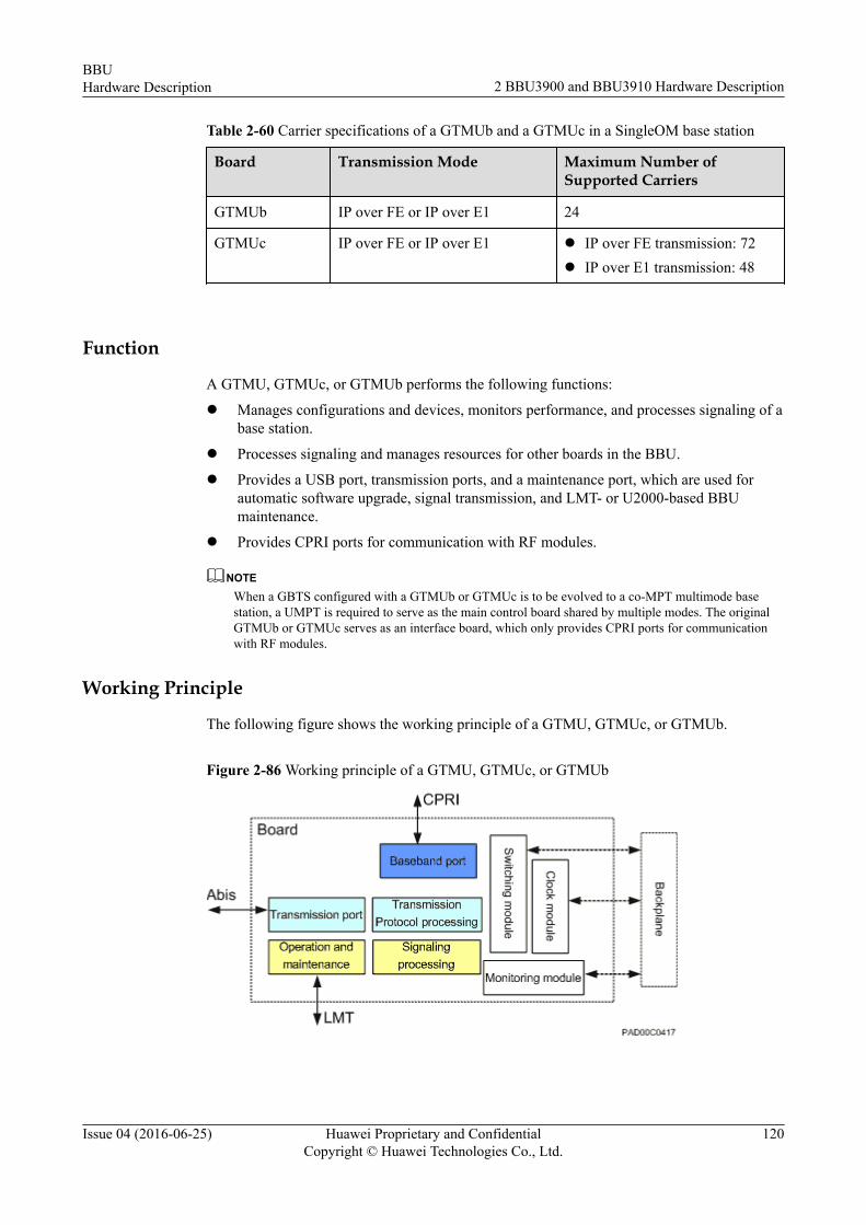
Table 2-60 Carrier specifications of a GTMUb and a GTMUc in a SingleOM base station
Board Transmission Mode Maximum Number ofSupported Carriers
GTMUb IP over FE or IP over E1 24
GTMUc IP over FE or IP over E1 l IP over FE transmission: 72l IP over E1 transmission: 48
Function
A GTMU, GTMUc, or GTMUb performs the following functions:
l Manages configurations and devices, monitors performance, and processes signaling of abase station.
l Processes signaling and manages resources for other boards in the BBU.
l Provides a USB port, transmission ports, and a maintenance port, which are used forautomatic software upgrade, signal transmission, and LMT- or U2000-based BBUmaintenance.
l Provides CPRI ports for communication with RF modules.
NOTEWhen a GBTS configured with a GTMUb or GTMUc is to be evolved to a co-MPT multimode basestation, a UMPT is required to serve as the main control board shared by multiple modes. The originalGTMUb or GTMUc serves as an interface board, which only provides CPRI ports for communicationwith RF modules.
Working Principle
The following figure shows the working principle of a GTMU, GTMUc, or GTMUb.
Figure 2-86 Working principle of a GTMU, GTMUc, or GTMUb
BBUHardware Description 2 BBU3900 and BBU3910 Hardware Description
Issue 04 (2016-06-25) Huawei Proprietary and ConfidentialCopyright © Huawei Technologies Co., Ltd.
120
PortThe following table describes the ports on GTMU boards.
Table 2-61 Ports on GTMU boards
Silkscreen Connector Description
E1/T1 DB26 femaleconnector
E1/T1 signal transmission port
EXT (on aGTMUb)
SFP femaleconnector
Reserved
l FE0 (on theGTMU/GTMUb)
l FE/GE0 (ona GTMUc)
RJ45 connector FE electrical signal transmission port
l FE1 (on aGTMU orGTMUb)
l FE/GE1 (ona GTMUc)
DLC connector FE optical signal transmission port
ETHa RJ45 connector Local maintenance and commissioning port
TSTb USB connector Port for clock signal outputs. The clock signalsare used for testing.
USBc USB connector USB loading port
CPRI0 toCPRI5
SFP femaleconnector
Data transmission ports connected to RFmodules. They support the input and output ofoptical and electrical transmission signals.
RST - Used for resetting the board
a: Before accessing a base station through an ETH port, ensure that an OM port has beenenabled and authorities for accessing the base station through the OM port have beenobtained.b: The USB commission port is used for commissioning the base station rather thanconfiguring and exporting information of the base station.c: The security of the USB port is ensured by encryption, and the USB port can be shutdown using commands.
The following table describes the specifications of CPRI ports on GTMU boards.
BBUHardware Description 2 BBU3900 and BBU3910 Hardware Description
Issue 04 (2016-06-25) Huawei Proprietary and ConfidentialCopyright © Huawei Technologies Co., Ltd.
121

Table 2-62 Specifications of CPRI ports on GTMU boards
Board Quantity of CPRIPorts
CPRI Port Rate(Gbit/s)
Topology Type
GTMU 6 1.25 Star, chain, and ringtopologies
GTMUb or GTMUc 6 1.25 or 2.5 Star, chain, and ringtopologies
DIP SwitchThere are four DIP switches on a GTMU, GTMUc, or GTMUb, which are S1, S2, S4, and S5.Figure 2-87 and Figure 2-88 show the positions of the DIP switches on a GTMU and aGTMUb or GTMUc, respectively.
Figure 2-87 Positions of DIP switches on a GTMU
BBUHardware Description 2 BBU3900 and BBU3910 Hardware Description
Issue 04 (2016-06-25) Huawei Proprietary and ConfidentialCopyright © Huawei Technologies Co., Ltd.
122

Figure 2-88 Positions of DIP switches on a GTMUb or GTMUc
The DIP switches perform the following functions:l S1 is used to select the E1/T1 mode.l S2 is used to select the grounding mode of E1/T1 reception.l S4 is used to select the E1 bypass.l S5 is used to set the timeslot when E1 bypass is selected.
Each DIP switch has four bits. Table 2-63, Table 2-64, Table 2-65, and Table 2-66 describethe bit settings and meanings of the DIP switches.
Table 2-63 DIP switch S1
DIPSwitch
Bit Setting Description
1 2 3 4
S1 ON ON - - The E1 resistance is setto 75 ohms.
OFF ON - - The E1 resistance is setto 120 ohms.
ON OFF - - The T1 resistance is setto 100 ohms.
ON ON OFF OFF The default setting isused.
Miscellaneous Unavailable
BBUHardware Description 2 BBU3900 and BBU3910 Hardware Description
Issue 04 (2016-06-25) Huawei Proprietary and ConfidentialCopyright © Huawei Technologies Co., Ltd.
123

NOTE
The default settings of bits 3 and 4 of DIP switch S1 are used, and onsite setting is not required. Theyshould be set to OFF by default. If the bits are set to ON, set them to OFF.
Table 2-64 DIP switch S2
DIPSwitch
Bit Setting Description
1 2 3 4
S2 OFF OFF OFF OFF All the bits are set toOFF by default in allmodes.
ON ON ON ON When the four RXlinks in E1 75 ohmmode have error bits,all bits of S2 must beset to ON to rectify thefaults on the E1 links.
ON ON ON ON The default setting isused.
Miscellaneous Unavailable
Table 2-65 DIP switch S4
DIPSwitch
Bit Setting Description
1 2 3 4
S4 ON ON ON ON Supporting E1 bypass
OFF OFF OFF OFF Not supporting E1bypass
ON ON ON ON The default setting isused.
Miscellaneous Unavailable
Table 2-66 DIP switch S5
DIPSwitch
Bit Setting Description
1 2 3 4
S5 ON ON ON ON Not supporting E1bypass
BBUHardware Description 2 BBU3900 and BBU3910 Hardware Description
Issue 04 (2016-06-25) Huawei Proprietary and ConfidentialCopyright © Huawei Technologies Co., Ltd.
124

DIPSwitch
Bit Setting Description
1 2 3 4
OFF ON ON OFF Supporting E1 bypassof one level ofcascaded base stations
ON OFF ON OFF Supporting E1 bypassof two levels ofcascaded base stations
OFF OFF ON OFF Supporting E1 bypassof three levels ofcascaded base stations
ON ON OFF OFF Supporting E1 bypassof four levels ofcascaded base stations
OFF ON OFF OFF Supporting E1 bypassof five levels ofcascaded base stations
ON ON ON ON The default setting isused.
Miscellaneous Unavailable
2.5.4 LMPTAn LMPT is an LTE main processing and transmission unit and can be installed in aBBU3900.
The following figure shows an LMPT panel.
Figure 2-89 LMPT panel
SpecificationsThe following table lists the transmission port specifications of an LMPT.
BBUHardware Description 2 BBU3900 and BBU3910 Hardware Description
Issue 04 (2016-06-25) Huawei Proprietary and ConfidentialCopyright © Huawei Technologies Co., Ltd.
125

Table 2-67 Transmission port specifications of an LMPT
Board ApplicableMode
Transmission Mode
Quantityof Ports
PortCapacity
Full/Half-Duplex
LMPT l LTEFDD
l LTETDD
Transmission overFE/GEoptical ports
2 100 Mbit/sor 1000Mbit/s
Full-duplex
Transmission overFE/GEelectricalports
2 10 Mbit/s,100 Mbit/s,or 1000Mbit/s
Full-duplex
The following table lists the signaling specifications of an LMPT working in LTE FDD mode.The BHCA specifications in the following table are based on the smart device traffic model.
Table 2-68 Signaling specifications of an LMPT working in LTE FDD mode
Board Signaling Specifications (BHCA)
LMPT 216000
The following table lists the signaling specifications of an LMPT working in LTE TDD mode.
Table 2-69 Signaling specifications of an LMPT working in LTE TDD mode
Board Signaling Specifications (BHCA)
LMPT 180000
The following table lists the maximum number of UEs in RRC connected mode supported byan LMPT.
Table 2-70 Maximum number of UEs in RRC connected mode
Board Datacard Traffic Model Smart Device Traffic Model
MaximumNumber ofUEs in RRCConnectedMode
MaximumNumber ofUplinkSynchronizedUEs
MaximumNumber ofUEs in RRCConnectedMode
MaximumNumber ofUplinkSynchronizedUEs
LMPT 5400 5400 1200 1200
BBUHardware Description 2 BBU3900 and BBU3910 Hardware Description
Issue 04 (2016-06-25) Huawei Proprietary and ConfidentialCopyright © Huawei Technologies Co., Ltd.
126
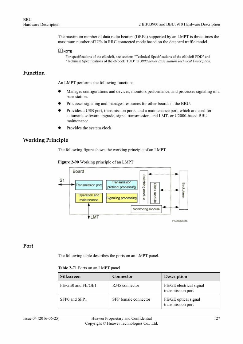
The maximum number of data radio bearers (DRBs) supported by an LMPT is three times themaximum number of UEs in RRC connected mode based on the datacard traffic model.
NOTEFor specifications of the eNodeB, see sections "Technical Specifications of the eNodeB FDD" and"Technical Specifications of the eNodeB TDD" in 3900 Series Base Station Technical Description.
Function
An LMPT performs the following functions:
l Manages configurations and devices, monitors performance, and processes signaling of abase station.
l Processes signaling and manages resources for other boards in the BBU.l Provides a USB port, transmission ports, and a maintenance port, which are used for
automatic software upgrade, signal transmission, and LMT- or U2000-based BBUmaintenance.
l Provides the system clock
Working Principle
The following figure shows the working principle of an LMPT.
Figure 2-90 Working principle of an LMPT
Port
The following table describes the ports on an LMPT panel.
Table 2-71 Ports on an LMPT panel
Silkscreen Connector Description
FE/GE0 and FE/GE1 RJ45 connector FE/GE electrical signaltransmission port
SFP0 and SFP1 SFP female connector FE/GE optical signaltransmission port
BBUHardware Description 2 BBU3900 and BBU3910 Hardware Description
Issue 04 (2016-06-25) Huawei Proprietary and ConfidentialCopyright © Huawei Technologies Co., Ltd.
127

Silkscreen Connector Description
GPS SMA connector Used for receiving GPSsignals
ETHa RJ45 connector Local maintenance andcommissioning port
TSTb USB connector Port for clock signal outputs.The clock signals are used fortesting.
USBc USB connector USB loading port
RST - Used for resetting the board
a: Before accessing a base station through an ETH port, ensure that an OM port has beenenabled and authorities for accessing the base station through the OM port have beenobtained.b: The USB commission port is used for commissioning the base station rather thanconfiguring and exporting information of the base station.c: The security of the USB port is ensured by encryption, and the USB port can be shutdown using commands.
NOTE
l Either SFP0 or FE/GE0 port on an LMPT is used for one GE input.
l Either SFP1 or FE/GE1 port on the LMPT is used for another GE input.
2.5.5 LPMPAn LPMP is an LTE passive intermodulation (PIM) mitigation processing card and can beinstalled in a BBU3900 or BBU3910.
The following figure shows an LPMP panel.
Figure 2-91 LPMP panel
SpecificationsThe following table lists the specifications of an LPMP working in LTE FDD mode.
BBUHardware Description 2 BBU3900 and BBU3910 Hardware Description
Issue 04 (2016-06-25) Huawei Proprietary and ConfidentialCopyright © Huawei Technologies Co., Ltd.
128
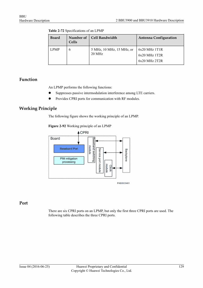
Table 2-72 Specifications of an LPMP
Board Number ofCells
Cell Bandwidth Antenna Configuration
LPMP 6 5 MHz, 10 MHz, 15 MHz, or20 MHz
6x20 MHz 1T1R6x20 MHz 1T2R6x20 MHz 2T2R
FunctionAn LPMP performs the following functions:l Suppresses passive intermodulation interference among LTE carriers.l Provides CPRI ports for communication with RF modules.
Working PrincipleThe following figure shows the working principle of an LPMP.
Figure 2-92 Working principle of an LPMP
PortThere are six CPRI ports on an LPMP, but only the first three CPRI ports are used. Thefollowing table describes the three CPRI ports.
BBUHardware Description 2 BBU3900 and BBU3910 Hardware Description
Issue 04 (2016-06-25) Huawei Proprietary and ConfidentialCopyright © Huawei Technologies Co., Ltd.
129
Table 2-73 Ports on an LPMP
Silkscreen Connector Quantity of Ports Description
CPRI0 to CPRI2 SFP femaleconnector
3 Interconnection datatransmission portsconnecting to RFmodules, whichsupport input andoutput of optical andelectricaltransmission signals
The following table lists the specifications of CPRI ports on an LPMP.
Table 2-74 Specifications of CPRI ports on an LPMP
Board Quantity of CPRIPorts
CPRI Port Rate(Gbit/s)
Topology Type
LPMP 3 1.25, 2.5, or 4.9 Star or chaintopology
The following table describes the mapping between the CPRI port rate and the number ofcells in an LTE FDD scenario.
Table 2-75 Mapping between the CPRI port rate and the number of cells in an LTE FDDscenario
CPRI Port Rate (Gbit/s) Number of 2x2 MIMO Cells
1.25 l 2 (cell bandwidth = 5 MHz)l 1 (cell bandwidth ≤ 10 MHz)
2.5 l 4 (cell bandwidth = 5 MHz)l 2 (cell bandwidth ≤ 10 MHz)l 1 (cell bandwidth = 15 MHz or 20 MHz)
4.9 l 4 (cell bandwidth ≤ 10 MHz)l 2 (cell bandwidth = 15 MHz or 20 MHz)
2.5.6 UBBPA UBBP is a universal baseband processing unit and can be installed in a BBU3900 orBBU3910.
The following figures show UBBP panels.
BBUHardware Description 2 BBU3900 and BBU3910 Hardware Description
Issue 04 (2016-06-25) Huawei Proprietary and ConfidentialCopyright © Huawei Technologies Co., Ltd.
130

NOTE
On the lower left corner of a board, there is a silkscreen indicating its type.
Figure 2-93 UBBPd panel
Figure 2-94 UBBPe panel
SpecificationsNOTE
A license is required to support board specifications.
The following table lists the types of UBBP boards.
Table 2-76 Types of UBBPd boards
Board Applicable Mode
l UBBPd1l UBBPd2
l GSMl UMTSl GU co-BBP
UBBPd3 l GSMl UMTSl LTE FDDl GU co-BBPl GL co-BBP
BBUHardware Description 2 BBU3900 and BBU3910 Hardware Description
Issue 04 (2016-06-25) Huawei Proprietary and ConfidentialCopyright © Huawei Technologies Co., Ltd.
131
Board Applicable Mode
UBBPd4 l GSMl UMTSl LTE FDDl LTE TDDl GU co-BBPl GL co-BBP
UBBPd5 l GSMl UMTSl LTE FDDl GU co-BBPl GL co-BBP
UBBPd6 l GSMl UMTSl LTE FDDl LTE TDDl GU co-BBPl GL co-BBPl UL co-BBPl GUL co-BBP
UBBPd9 LTE TDD
UBBPda LTE FDD
Table 2-77 Types of UBBPe boards
Board Applicable Mode
UBBPe1 l UMTSl LTE FDD
UBBPe2 l UMTSl LTE FDD
UBBPe3 l UMTSl LTE FDDl UL co-BBP
UBBPe4 or UBBPe6 l UMTSl LTE FDDl LTE TDDl UL co-BBP
BBUHardware Description 2 BBU3900 and BBU3910 Hardware Description
Issue 04 (2016-06-25) Huawei Proprietary and ConfidentialCopyright © Huawei Technologies Co., Ltd.
132

Board Applicable Mode
UBBPe5 l UMTSl LTE FDDl UL co-BBP
UBBPe9 LTE TDD
NOTE
Co-BBP enables one baseband processing board to process baseband signals for multiple modes. Co-BBP issupported only in co-MPT base stations. For co-BBP specifications of UBBP boards working in multiplemodes, see Technical Specifications of the Multimode Base Station in 3900 Series Base Station TechnicalDescription.
Specifications of UBBP boards working in GSM mode
The following table lists the number of carriers supported by UBBP boards working in GSMmode.
Table 2-78 Carrier specifications
Board Number of 2R Carriers Number of 4R Carriers
UBBPd1, UBBPd2,UBBPd3, or UBBPd4
24 12
UBBPd5 36 18
UBBPd6 48 24
Specifications of UBBP boards working in UMTS mode
Table 2-79 lists the baseband specifications of UBBP boards working in UMTS mode.
Table 2-79 Baseband specifications
Board Numberof Cellsa
NumberofUplinkCEs
NumberofDownlink CEs
NumberofHSDPACodes
NumberofHSDPAUEs
NumberofHSUPAUEs
UBBPd1 6 384 512 6x15 288 288
UBBPd2 6 512 768 6x15 384 384
UBBPd3 6 384 512 6x15 288 288
UBBPd4 6 512 768 6x15 384 384
UBBPd5 6 768 768 6x15 512 512
UBBPd6 12 1024 1024 12x15 768 768
BBUHardware Description 2 BBU3900 and BBU3910 Hardware Description
Issue 04 (2016-06-25) Huawei Proprietary and ConfidentialCopyright © Huawei Technologies Co., Ltd.
133

Board Numberof Cellsa
NumberofUplinkCEs
NumberofDownlink CEs
NumberofHSDPACodes
NumberofHSDPAUEs
NumberofHSUPAUEs
UBBPe1 6 384 512 6x15 288 288
UBBPe2 6 512 768 6x15 384 384
UBBPe3 12 768 768 12x15 512 512
UBBPe4 12 1024 1024 12x15 768 768
UBBPe5 12 1024 1024 12x15 768 768
UBBPe6 12 1024 1024 12x15 768 768
a: indicates the number of 1T2R cells. The quantity of baseband resources consumed bycells varies depending on cell types, and therefore the number of cells supported by abaseband processing board varies depending on cell types. For details, see chapter"Consumption Principles of Baseband Resources" in NodeB Baseband ResourceManagement Feature Parameter Description by choosing 3900 Series Base StationProduct Documentation > Description > Function Description.
NOTE
For combined signaling specifications of a board, see section "Technical Specifications of the BBU3900s andBBU3910s" in 3900 Series Base Station Technical Description.
Specifications of UBBP boards working in LTE FDD mode
Table 2-80, Table 2-81, and Table 2-82 list the specifications of cells, the maximum numberof UEs in RRC connected mode, and maximum uplink and downlink throughput supported byUBBP boards working in LTE FDD mode, respectively. Table 2-83 lists the signalingspecifications supported by UBBP boards working in LTE FDD mode.
Table 2-80 Cell specifications of a UBBP
Board Number of Cells Cell Bandwidth(MHz)
AntennaConfiguration
UBBPd3 3 1.4/3/5/10/15/20 3x20 MHz 1T1R3x20 MHz 1T2R3x20 MHz 2T2R
UBBPd4 3 1.4/3/5/10/15/20 3x20 MHz 1T1R3x20 MHz 1T2R3x20 MHz 2T2R3x20 MHz 2T4R3x20 MHz 4T4R
BBUHardware Description 2 BBU3900 and BBU3910 Hardware Description
Issue 04 (2016-06-25) Huawei Proprietary and ConfidentialCopyright © Huawei Technologies Co., Ltd.
134

Board Number of Cells Cell Bandwidth(MHz)
AntennaConfiguration
UBBPd5 6 1.4/3/5/10/15/20 6x20 MHz 1T1R6x20 MHz 1T2R6x20 MHz 2T2R3x20 MHz 4T4R
UBBPd6 6 1.4/3/5/10/15/20 6x20 MHz 1T1R6x20 MHz 1T2R6x20 MHz 2T2R6x20 MHz 2T4R6x20 MHz 4T4R
UBBPda 6 1.4/3/5/10/15/20 6x10 MHz 2T4R6x20 MHz 1T1R6x20 MHz 1T2R6x20 MHz 2T2R
UBBPe1 3 1.4/3/5/10/15/20 3x20 MHz 1T1R3x20 MHz 1T2R3x20 MHz 2T2R
UBBPe2 3 1.4/3/5/10/15/20 3x20 MHz 1T1R3x20 MHz 1T2R3x20 MHz 2T2R3x20 MHz 2T4R3x20 MHz 4T4R
UBBPe3 6 1.4/3/5/10/15/20 6x20 MHz 1T1R6x20 MHz 1T2R6x20 MHz 2T2R
UBBPe4 6 1.4/3/5/10/15/20 6x20 MHz 1T1R6x20 MHz 1T2R6x20 MHz 2T2R6x20 MHz 2T4R6x20 MHz 4T4R
UBBPe5 9 1.4/3/5/10/15/20 9x20 MHz 1T1R9x20 MHz 1T2R9x20 MHz 2T2R9x20 MHz 2T4R9x20 MHz 4T4R
BBUHardware Description 2 BBU3900 and BBU3910 Hardware Description
Issue 04 (2016-06-25) Huawei Proprietary and ConfidentialCopyright © Huawei Technologies Co., Ltd.
135
Board Number of Cells Cell Bandwidth(MHz)
AntennaConfiguration
UBBPe6 12 1.4/3/5/10/15/20 12x20 MHz 1T1R12x20 MHz 1T2R12x20 MHz 2T2R12x20 MHz 2T4R12x20 MHz 4T4R
NOTE
l 1R and 2R cells can be configured together in any forms. In hybrid configuration, the total number ofcells cannot exceed the number of 2R cells supported by the eNodeB.
l The UBBPda does not support the hybrid configuration of 1R and 4R cells, or 2R and 4R cells.
l The UBBPd4/UBBPd5 supports hybrid configuration of 1R and 4R cells, or 2R and 4R cells. In hybridconfiguration, a maximum of three cells are supported.
l The UBBPd6 supports hybrid configuration of 1R and 4R cells, or 2R and 4R cells. In hybridconfiguration, a maximum of six cells are supported.
Table 2-81 Maximum number of UEs in RRC Connected mode supported by the UBBP board
Board CellBandwidth
Datacard Traffic Model Smartphone TrafficModel
MaximumNumber ofUEs inRRCConnectedMode
MaximumNumber ofUplinkSynchronized UEs
MaximumNumber ofUEs inRRCConnectedMode
MaximumNumber ofUplinkSynchronized UEs
UBBPd3/UBBPd4
1.4 MHz 504 504 504 504
3 MHz 1080 1080 1080 1080
5 MHz 1800 1800 1500 1500
10/15/20MHz
3600 3600 1500 1500
UBBPd5/UBBPd6/UBBPda
1.4 MHz 1008 1008 1008 1008
3 MHz 2160 2160 2160 2160
5/10/15/20MHz
3600 3600 2200 2200
UBBPe1/UBBPe2
1.4 MHz 504 504 504 504
3 MHz 1080 1080 1080 1080
5 MHz 1800 1800 1500 1500
BBUHardware Description 2 BBU3900 and BBU3910 Hardware Description
Issue 04 (2016-06-25) Huawei Proprietary and ConfidentialCopyright © Huawei Technologies Co., Ltd.
136

Board CellBandwidth
Datacard Traffic Model Smartphone TrafficModel
MaximumNumber ofUEs inRRCConnectedMode
MaximumNumber ofUplinkSynchronized UEs
MaximumNumber ofUEs inRRCConnectedMode
MaximumNumber ofUplinkSynchronized UEs
10/15/20MHz
3600 3600 1500 1500
UBBPe3/UBBPe4
1.4 MHz 1008 1008 1008 1008
3 MHz 2160 2160 2160 2160
5/10/15/20MHz
3600 3600 2400 2400
UBBPe5 1.4 MHz 1512 1512 1512 1512
3 MHz 3240 3240 3000 3000
5/10/15/20MHz
3600 3600 3000 3000
UBBPe6 1.4 MHz 2016 2016 2016 2016
3M Hz 4320 4320 3600 3600
5/10/15/20MHz
4800 4800 3600 3600
Table 2-82 Throughput
Board Maximum DownlinkThroughput (Mbit/s)
Maximum UplinkThroughput (Mbit/s)
UBBPd3 450 225
UBBPd4 600 225
UBBPd5 or UBBPda 600 300
UBBPd6 1200 600
UBBPe1 450 225
UBBPe2 600 300
UBBPe3 600 300
UBBPe4 1200 600
UBBPe5 1200 600
BBUHardware Description 2 BBU3900 and BBU3910 Hardware Description
Issue 04 (2016-06-25) Huawei Proprietary and ConfidentialCopyright © Huawei Technologies Co., Ltd.
137

Board Maximum DownlinkThroughput (Mbit/s)
Maximum UplinkThroughput (Mbit/s)
UBBPe6 2400 1200
Table 2-83 Signaling specifications
Board Signaling Specifications (BHCA)a
UBBPd3/UBBPd4 270000
UBBPd5/UBBPd6/UBBPda 396000
UBBPe1/UBBPe2 324000
UBBPe3/UBBPe4 432000
UBBPe5 540000
UBBPe6 648000
a: The BHCA specifications are based on the smart device traffic model.
The maximum number of data radio bearers (DRBs) supported by a UBBP is three times themaximum number of UEs in RRC connected mode based on the datacard traffic model.
Specifications of UBBP boards working in LTE TDD mode
Table 2-84, Table 2-85, Table 2-86, and Table 2-87 list the specifications of cells, maximumnumber of UEs in RRC connected mode, maximum uplink and downlink throughput, andsignaling specifications supported by UBBP boards working in LTE TDD mode, respectively.
Table 2-84 Cell specifications of a UBBP
Board Number of Cells Cell Bandwidth(MHz)
AntennaConfiguration
UBBPd4 3 5/10/15/20 3x20 MHz 2T2R3x20 MHz 4T4R
UBBPd6 6 5/10/15/20 6x20 MHz 2T2R6x20 MHz 4T4R
UBBPd9 3 10/15/20 3x20 MHz 8T8R
UBBPe4 6 5/10/15/20 6x20 MHz 2T2R6x20 MHz 4T4R
3 10/15/20 3x20 MHz 8T8R
UBBPe6 12 5/10/15/20 12x20 MHz 2T2R12x20 MHz 4T4R
BBUHardware Description 2 BBU3900 and BBU3910 Hardware Description
Issue 04 (2016-06-25) Huawei Proprietary and ConfidentialCopyright © Huawei Technologies Co., Ltd.
138

Board Number of Cells Cell Bandwidth(MHz)
AntennaConfiguration
6 10/15/20 6x20 MHz 8T8R
UBBPe9 12 5/10/15/20 12x20 MHz 2T2R12x20 MHz 4T4R
12 10/15/20 12x20 MHz 8T8R
Table 2-85 Maximum number of UEs in RRC Connected mode supported by the UBBP board
Board CellBandwidth
MaximumNumber of UEsin RRCConnected Mode(Datacard TrafficModel)
Maximum Number of UEs in RRCConnected Mode (SmartphoneTraffic Model)
UBBPd4
5 MHz 1800 900
10/15/20MHz
3600 1500
UBBPd6
5 MHz 1800 1800
10/15/20MHz
3600 2200
UBBPd9
10 MHz 3600 1800
15/20 MHz 3600 2200
UBBPe4
5/10/15/20MHz
3600 2400
UBBPe6/UBBPe9
5/10/15/20MHz
4800 3600
Table 2-86 Throughput
Board Maximum DownlinkThroughput (Mbit/s)
Maximum UplinkThroughput (Mbit/s)
UBBPd4 600 225
UBBPd6 1200 600
UBBPd9 1200 600
UBBPe4 1200 600
BBUHardware Description 2 BBU3900 and BBU3910 Hardware Description
Issue 04 (2016-06-25) Huawei Proprietary and ConfidentialCopyright © Huawei Technologies Co., Ltd.
139

Board Maximum DownlinkThroughput (Mbit/s)
Maximum UplinkThroughput (Mbit/s)
UBBPe6 2400 1200
UBBPe9 2400 1200
Table 2-87 Signaling specifications
Board Signaling Specifications (BHCA)
UBBPd4 270000
UBBPd6 or UBBPd9 396000
UBBPe4 432000
UBBPe6/UBBPe9 648000
NOTE
The signaling specifications for TDD scenarios are the maximum ones for typical scenarios of normalcells.
The maximum number of DRBs supported by a UBBP is three times the maximum number ofUEs in RRC connected mode.
NOTEFor specifications of an eNodeB, see section "Technical Specifications of the BBU3900s andBBU3910s" in 3900 Series Base Station Technical Description.
FunctionA UBBP performs the following functions:l Provides CPRI ports for communication with RF modules.l Processes uplink and downlink baseband signals.l Supports the multiplex of baseband resources among different modes, thereby
implementing multimode concurrency.
Working PrincipleThe following figure shows the working principle of a UBBP.
BBUHardware Description 2 BBU3900 and BBU3910 Hardware Description
Issue 04 (2016-06-25) Huawei Proprietary and ConfidentialCopyright © Huawei Technologies Co., Ltd.
140
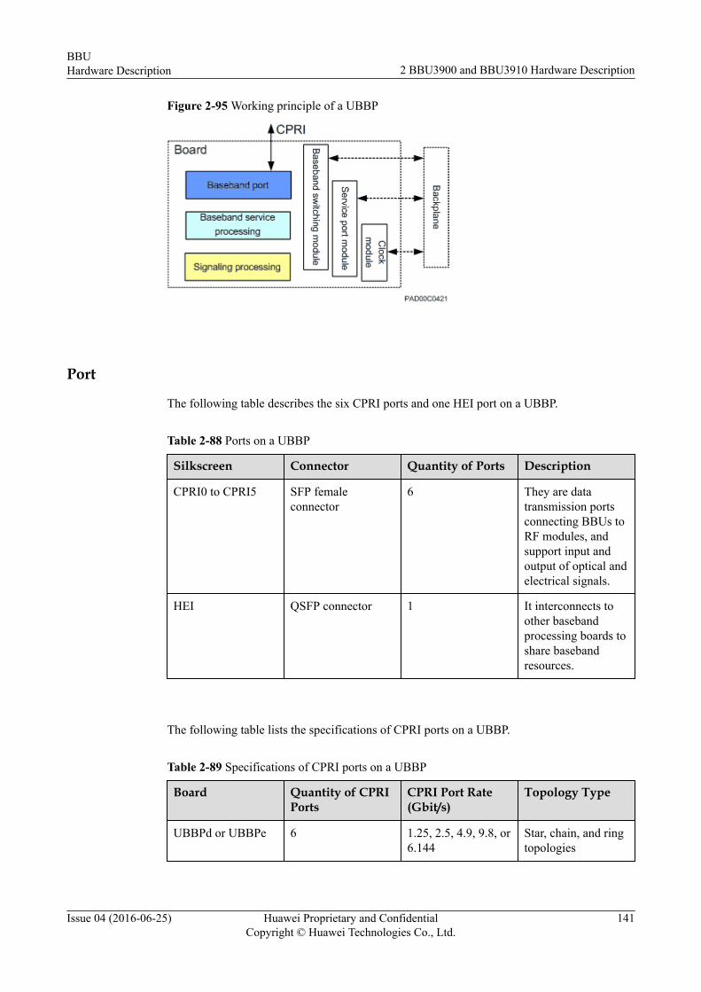
Figure 2-95 Working principle of a UBBP
Port
The following table describes the six CPRI ports and one HEI port on a UBBP.
Table 2-88 Ports on a UBBP
Silkscreen Connector Quantity of Ports Description
CPRI0 to CPRI5 SFP femaleconnector
6 They are datatransmission portsconnecting BBUs toRF modules, andsupport input andoutput of optical andelectrical signals.
HEI QSFP connector 1 It interconnects toother basebandprocessing boards toshare basebandresources.
The following table lists the specifications of CPRI ports on a UBBP.
Table 2-89 Specifications of CPRI ports on a UBBP
Board Quantity of CPRIPorts
CPRI Port Rate(Gbit/s)
Topology Type
UBBPd or UBBPe 6 1.25, 2.5, 4.9, 9.8, or6.144
Star, chain, and ringtopologies
BBUHardware Description 2 BBU3900 and BBU3910 Hardware Description
Issue 04 (2016-06-25) Huawei Proprietary and ConfidentialCopyright © Huawei Technologies Co., Ltd.
141
The following table lists the mapping between the CPRI port rate and the number of carrierssupported by a UBBP working in GSM mode.
Table 2-90 Mapping between the CPRI port rate and the number of carriers
CPRI Port Rate (Gbit/s) Number of 1T2RCarriers
Number of 2T2R or 1T4RCarriers
1.25 24 12
2.5 48 24
4.9 48 24
9.8 48 24
The following table lists the mapping between the CPRI port rate and the number of cellssupported by a UBBP working in UMTS mode.
Table 2-91 Mapping between the CPRI port rate and the number of cells in UMTS scenarios
CPRI Port Rate (Gbit/s) Number of 1T2R Cells Number of 2T2R Cells
1.25 4 4*a
2.5 8 8*a
4.9 16 16*a
6.144 24 24*a
9.8 32 32*a
a: The asterisk (*) in the table indicates that the number of 2T2R cells is halved if the 2T2Rcells support the virtual antenna mapping (VAM) function and the two TX antennas usedby the VAM function are separately connected to two RF modules carried on differentCPRI links.
The following table lists the mapping between the CPRI port rate and the number of cellssupported by a UBBP working in LTE FDD mode.
BBUHardware Description 2 BBU3900 and BBU3910 Hardware Description
Issue 04 (2016-06-25) Huawei Proprietary and ConfidentialCopyright © Huawei Technologies Co., Ltd.
142

Table 2-92 Mapping between the CPRI port rate and the number of cells in an LTE FDDscenario
CPRI Port Rate(Gbit/s)
Number of 2T4Ror 4T4R Cells
Number of 1T2Ror 2T2R Cells
Number of 1T1RCells
1.25 4x4 MIMO cells arenot recommendedbecause thetransmissionbandwidth of CPRIports is limited.
l 4 (cell bandwidth≤ 3 MHz)
l 2 (cell bandwidth≤ 5 MHz)
l 1 (cell bandwidth≤ 10 MHz)
l 8 (cell bandwidth≤ 3 MHz)
l 4 (cell bandwidth≤ 5 MHz)
l 2 (cell bandwidth≤ 10 MHz)
l 1 (cell bandwidth= 15 MHz or 20MHz)
2.5 1 (cell bandwidth ≤10 MHz)
l 4 (cell bandwidth≤ 5 MHz)
l 2 (cell bandwidth≤ 10 MHz)
l 1 (cell bandwidth= 15 MHz or 20MHz)
l 8 (cell bandwidth≤ 5 MHz)
l 4 (cell bandwidth≤ 10 MHz)
l 2 (cell bandwidth= 15 MHz or 20MHz)
4.9 l 2 (cell bandwidth≤ 10 MHz)
l 1 (cell bandwidth= 15 MHz or 20MHz)
l 4 (cell bandwidth≤ 10 MHz)
l 2 (cell bandwidth= 15 MHz or 20MHz)
l 8 (cell bandwidth≤ 10 MHz)
l 4 (cell bandwidth= 15 MHz or 20MHz)
6.144 l 2 (cell bandwidth≤ 10 MHz)
l 1 (cell bandwidth= 15 MHz or 20MHz)
l 5 (cell bandwidth≤ 10 MHz)
l 2 (cell bandwidth= 15 MHz or 20MHz)
l 10 (cellbandwidth ≤ 10MHz)
l 5 (cell bandwidth= 15 MHz or 20MHz)
9.8 l 4 (cell bandwidth≤ 10 MHz)
l 2 (cell bandwidth= 15 MHz or 20MHz)
l 8 (cell bandwidth≤ 10 MHz)
l 4 (cell bandwidth= 15 MHz or 20MHz)
l 16 (cellbandwidth ≤ 10MHz)
l 8 (cell bandwidth= 15 MHz or 20MHz)
The following table lists the mapping between the CPRI port rate and the number of cellssupported by a UBBP working in LTE TDD mode.
BBUHardware Description 2 BBU3900 and BBU3910 Hardware Description
Issue 04 (2016-06-25) Huawei Proprietary and ConfidentialCopyright © Huawei Technologies Co., Ltd.
143

Table 2-93 Mapping between the CPRI port rate and the number of cells in an LTE TDDscenario
CPRI PortRate (Gbit/s)
CPRICompression
Number of8T8R Cells
Number of4T4R Cells
Number of2T2R Cells
2.5 Not in use None l 2 (cellbandwidth =5 MHz)
l 1 (cellbandwidth =10 MHz)
l None (cellbandwidth =15 MHz or20 MHz)
l 4 (cellbandwidth =5 MHz)
l 2 (cellbandwidth =10 MHz)
l 1 (cellbandwidth =15 MHz or20 MHz)
In use None l None (cellbandwidth =5 MHz)
l 1 (cellbandwidth =10 MHz)
l 1 (cellbandwidth =15 MHz or20 MHz)
l None (cellbandwidth =5 MHz)
l 3 (cellbandwidth =10 MHz)
l 2 (cellbandwidth =15 MHz or20 MHz)
4.9 Not in use l None (cellbandwidth =5 MHz)
l 1 (cellbandwidth =10 MHz)
l None (cellbandwidth =15 MHz or20 MHz)
l 4 (cellbandwidth =5 MHz)
l 2 (cellbandwidth =10 MHz)
l 1 (cellbandwidth =15 MHz or20 MHz)
l 8 (cellbandwidth =5 MHz)
l 4 (cellbandwidth =10 MHz)
l 2 (cellbandwidth =15 MHz or20 MHz)
In use l None (cellbandwidth =5 MHz)
l 1 (cellbandwidth =10 MHz)
l 1 (cellbandwidth =15 MHz or20 MHz)
l None (cellbandwidth =5 MHz)
l 3 (cellbandwidth =10 MHz)
l 2 (cellbandwidth =15 MHz or20 MHz)
l None (cellbandwidth =5 MHz)
l 6 (cellbandwidth =10 MHz)
l 4 (cellbandwidth =15 MHz or20 MHz)
BBUHardware Description 2 BBU3900 and BBU3910 Hardware Description
Issue 04 (2016-06-25) Huawei Proprietary and ConfidentialCopyright © Huawei Technologies Co., Ltd.
144

CPRI PortRate (Gbit/s)
CPRICompression
Number of8T8R Cells
Number of4T4R Cells
Number of2T2R Cells
9.8 Not in use l None (cellbandwidth =5 MHz)
l 2 (cellbandwidth =10 MHz)
l 1 (cellbandwidth =15 MHz or20 MHz)
l 8 (cellbandwidth =5 MHz)
l 4 (cellbandwidth =10 MHz)
l 2 (cellbandwidth =15 MHz or20 MHz)
l 16 (cellbandwidth =5 MHz)
l 8 (cellbandwidth =10 MHz)
l 4 (cellbandwidth =15 MHz or20 MHz)
In use l None (cellbandwidth =5 MHz or 15MHz)
l 3 (cellbandwidth =10 MHz)
l 2 (cellbandwidth =20 MHz)
l None (cellbandwidth =5 MHz or 15MHz)
l 6 (cellbandwidth =10 MHz)
l 4 (cellbandwidth =20 MHz)
l None (cellbandwidth =5 MHz or 15MHz)
l 12 (cellbandwidth =10 MHz)
l 8 (cellbandwidth =20 MHz)
2.5.7 WBBPA WBBP is a WCDMA baseband processing unit and can be installed in a BBU3900.
Figure 2-96 shows the exterior of a WBBPa panel.
Figure 2-97 shows the exterior of a WBBPb1, WBBPb2, WBBPb3, or WBBPb4 panel.
Figure 2-98 shows the exterior of a WBBPd1, WBBPd2, or WBBPd3 panel.
Figure 2-99 shows the exterior of a WBBPf1, WBBPf2, WBBPf3, or WBBPf4 panel.
NOTE
l There is no label indicating the board type on the lower left corner of a WBBPa.l On a WBBPb1, a WBBPb2, a WBBPb3, and a WBBPb4, there are silkscreens WBBPb1, WBBPb2,
WBBPb3, and WBBPb4, respectively. Figure 2-97 shows a WBBPb1 panel.l On a WBBPd1, a WBBPd2, and a WBBPd3, there are silkscreens WBBPd1, WBBPd2, and
WBBPd3, respectively. Figure 2-98 shows a WBBPd1 panel.l On a WBBPf1, a WBBPf2, a WBBPf3, and a WBBPf4, there are silkscreens WBBPf1, WBBPf2,
WBBPf3, and WBBPf4, respectively. Figure 2-99 shows a WBBPf1 panel.
Figure 2-96 WBBPa panel
BBUHardware Description 2 BBU3900 and BBU3910 Hardware Description
Issue 04 (2016-06-25) Huawei Proprietary and ConfidentialCopyright © Huawei Technologies Co., Ltd.
145

Figure 2-97 WBBPb panel
Figure 2-98 WBBPd panel
Figure 2-99 WBBPf panel
SpecificationsNOTE
A license is required to support board specifications.
The WBBP is classified into four types, as listed in Table 2-94.
NOTE
The baseband processing board in slot 2 or 3 in a BBU3900 can transfer received CPRI data to otherboards.
Table 2-94 Specifications of the WBBP
Board Numberof Cellsa
Numberof ULCEs
Numberof DLCEs
NumberofHSDPACodesb
NumberofHSDPAUEs
NumberofHSUPAUEs
WBBPa 3 128 256 3x15 96 60
WBBPb1 3 64 64 3x15 64 64
WBBPb2 3 128 128 3x15 128 96
BBUHardware Description 2 BBU3900 and BBU3910 Hardware Description
Issue 04 (2016-06-25) Huawei Proprietary and ConfidentialCopyright © Huawei Technologies Co., Ltd.
146

Board Numberof Cellsa
Numberof ULCEs
Numberof DLCEs
NumberofHSDPACodesb
NumberofHSDPAUEs
NumberofHSUPAUEs
WBBPb3 6 256 256 6x15 144 96
WBBPb4 6 384 384 6x15 144 96
WBBPd1 6 192 192 6x15 128 96
WBBPd2 6 384 384 6x15 144 144
WBBPd3 6 256 256 6x15 144 96
WBBPf1 6 192 256 6x15 144 144
WBBPf2 6 256 384 6x15 192 192
WBBPf3 6 384 512 6x15 256 256
WBBPf4 6 512 768 6x15 384 384
a: indicates the number of 1T2R cells. The quantity of baseband resources consumed bycells varies depending on cell types, and therefore the number of cells supported by abaseband processing board varies depending on cell types. For details, see chapter"Consumption Principles of Baseband Resources" in NodeB Baseband ResourceManagement Feature Parameter Description by choosing 3900 Series Base StationProduct Documentation > Description > Function Description.b: The number of HSDPA codes supported by a WBBPd1 is 6x15, in which 6 is the numberof cells and 15 is the number of HSDPA codes supported by each cell.
NOTEFor combined signaling specifications of a board, see section "Technical Specifications of theBBU3900s and BBU3910s" in 3900 Series Base Station Technical Description.
Functionl A WBBP processes uplink and downlink baseband signals.l A WBBP provides CPRI ports for communication with RF modules.l A WBBPd supports interference cancellation (IC) within the board.l When CPRI cables connect RF modules carrying corresponding cells to a WBBPd, the
WBBPd installed in slot 2 or 3 supports interference cancellation (IC) of uplink data.l A WBBPf installed in slot 2 or 3 supports baseband interconnection between BBUs.
Working PrincipleThe following figure shows the working principle of a WBBP.
BBUHardware Description 2 BBU3900 and BBU3910 Hardware Description
Issue 04 (2016-06-25) Huawei Proprietary and ConfidentialCopyright © Huawei Technologies Co., Ltd.
147

Figure 2-100 Working principle of a WBBP
PortThe following table describes the six CPRI ports on WBBPa and WBBPb panels.
Table 2-95 Ports on WBBPa and WBBPb panels
Board Type Silkscreen Connector Description
WBBPa CPRI0, CPRI1, andCPRI2
SFP femaleconnector
They are datatransmission portsconnecting BBUs toRF modules, andsupport input andoutput of optical andelectrical signals.
WBBPb CPRI0/EIH0,CPRI1/EIH1, andCPRI2/EIH2
Table 2-96 describes the six CPRI ports on a WBBPd.
Table 2-96 Ports on a WBBPd panel
Silkscreen Connector Description
CPRI0, CPRI1,CPRI2, CPRI3/EIH0, CPRI4/EIH1,and CPRI5/EIH2
SFP female connector They are data transmission portsconnecting BBUs to RFmodules, and support input andoutput of optical and electricalsignals.
Table 2-97 describes the six CPRI ports and one HEI port on a WBBPf.
BBUHardware Description 2 BBU3900 and BBU3910 Hardware Description
Issue 04 (2016-06-25) Huawei Proprietary and ConfidentialCopyright © Huawei Technologies Co., Ltd.
148

Table 2-97 Ports on the WBBPf panel
Silkscreen Connector Description
CPRI0, CPRI1,CPRI2, CPRI3,CPRI4, and CPRI5
SFP female connector They are data transmission portsconnecting BBUs to RFmodules, and support input andoutput of optical and electricalsignals.
HEI QSFP connector It interconnects to otherbaseband processing boards toshare baseband resources.
The following table lists the specifications of CPRI ports on a WBBP.
Table 2-98 Specifications of CPRI ports on a WBBP
Board Quantity of CPRIPorts
CPRI Port Rate(Gbit/s)
Topology Type
WBBPa 3 1.25 Star, chain, and ringtopologies
WBBPb1, WBBPb2,WBBPb3, orWBBPb4
3 1.25/2.5 Star, chain, and ringtopologies
WBBPd 6 1.25 or 2.5 Star, chain, and ringtopologies
WBBPf 6 1.25, 2.5, 4.9, or6.144
Star, chain, and ringtopologies
CPRI ports with different data rates support different numbers of cells, as listed in thefollowing table.
Table 2-99 Mapping between CPRI data rate and number of cells supported
CPRI Port Rate (Gbit/s) Number of 1T2R Cells Number of 2T2R Cells
1.25 4 4*a
2.5 8 8*a
4.9 16 16*a
6.144 24 24*a
BBUHardware Description 2 BBU3900 and BBU3910 Hardware Description
Issue 04 (2016-06-25) Huawei Proprietary and ConfidentialCopyright © Huawei Technologies Co., Ltd.
149
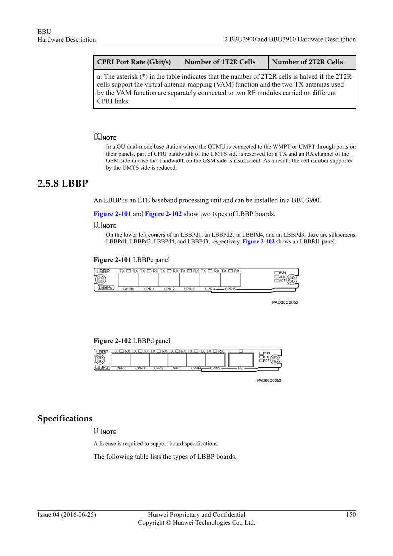
CPRI Port Rate (Gbit/s) Number of 1T2R Cells Number of 2T2R Cells
a: The asterisk (*) in the table indicates that the number of 2T2R cells is halved if the 2T2Rcells support the virtual antenna mapping (VAM) function and the two TX antennas usedby the VAM function are separately connected to two RF modules carried on differentCPRI links.
NOTEIn a GU dual-mode base station where the GTMU is connected to the WMPT or UMPT through ports ontheir panels, part of CPRI bandwidth of the UMTS side is reserved for a TX and an RX channel of theGSM side in case that bandwidth on the GSM side is insufficient. As a result, the cell number supportedby the UMTS side is reduced.
2.5.8 LBBPAn LBBP is an LTE baseband processing unit and can be installed in a BBU3900.
Figure 2-101 and Figure 2-102 show two types of LBBP boards.
NOTEOn the lower left corners of an LBBPd1, an LBBPd2, an LBBPd4, and an LBBPd3, there are silkscreensLBBPd1, LBBPd2, LBBPd4, and LBBPd3, respectively. Figure 2-102 shows an LBBPd1 panel.
Figure 2-101 LBBPc panel
Figure 2-102 LBBPd panel
SpecificationsNOTE
A license is required to support board specifications.
The following table lists the types of LBBP boards.
BBUHardware Description 2 BBU3900 and BBU3910 Hardware Description
Issue 04 (2016-06-25) Huawei Proprietary and ConfidentialCopyright © Huawei Technologies Co., Ltd.
150
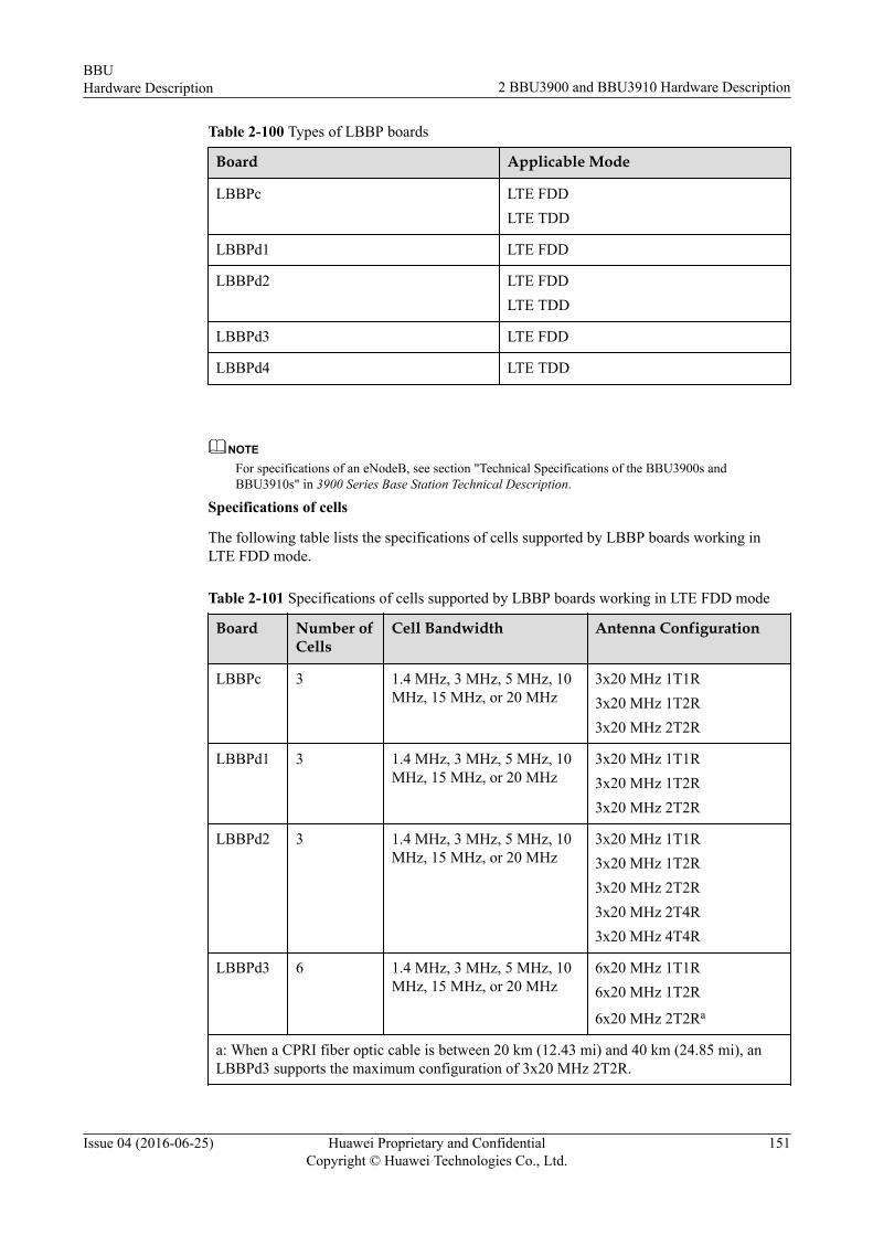
Table 2-100 Types of LBBP boards
Board Applicable Mode
LBBPc LTE FDDLTE TDD
LBBPd1 LTE FDD
LBBPd2 LTE FDDLTE TDD
LBBPd3 LTE FDD
LBBPd4 LTE TDD
NOTEFor specifications of an eNodeB, see section "Technical Specifications of the BBU3900s andBBU3910s" in 3900 Series Base Station Technical Description.
Specifications of cells
The following table lists the specifications of cells supported by LBBP boards working inLTE FDD mode.
Table 2-101 Specifications of cells supported by LBBP boards working in LTE FDD mode
Board Number ofCells
Cell Bandwidth Antenna Configuration
LBBPc 3 1.4 MHz, 3 MHz, 5 MHz, 10MHz, 15 MHz, or 20 MHz
3x20 MHz 1T1R3x20 MHz 1T2R3x20 MHz 2T2R
LBBPd1 3 1.4 MHz, 3 MHz, 5 MHz, 10MHz, 15 MHz, or 20 MHz
3x20 MHz 1T1R3x20 MHz 1T2R3x20 MHz 2T2R
LBBPd2 3 1.4 MHz, 3 MHz, 5 MHz, 10MHz, 15 MHz, or 20 MHz
3x20 MHz 1T1R3x20 MHz 1T2R3x20 MHz 2T2R3x20 MHz 2T4R3x20 MHz 4T4R
LBBPd3 6 1.4 MHz, 3 MHz, 5 MHz, 10MHz, 15 MHz, or 20 MHz
6x20 MHz 1T1R6x20 MHz 1T2R
6x20 MHz 2T2Ra
a: When a CPRI fiber optic cable is between 20 km (12.43 mi) and 40 km (24.85 mi), anLBBPd3 supports the maximum configuration of 3x20 MHz 2T2R.
BBUHardware Description 2 BBU3900 and BBU3910 Hardware Description
Issue 04 (2016-06-25) Huawei Proprietary and ConfidentialCopyright © Huawei Technologies Co., Ltd.
151
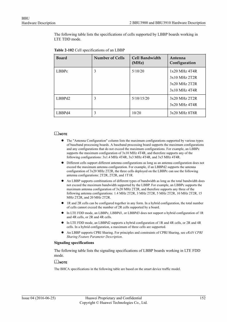
The following table lists the specifications of cells supported by LBBP boards working inLTE TDD mode.
Table 2-102 Cell specifications of an LBBP
Board Number of Cells Cell Bandwidth(MHz)
AntennaConfiguration
LBBPc 3 5/10/20 1x20 MHz 4T4R3x10 MHz 2T2R3x20 MHz 2T2R3x10 MHz 4T4R
LBBPd2 3 5/10/15/20 3x20 MHz 2T2R3x20 MHz 4T4R
LBBPd4 3 10/20 3x20 MHz 8T8R
NOTE
l The "Antenna Configuration" column lists the maximum configurations supported by various typesof baseband processing boards. A baseband processing board supports the maximum configurationsand any configurations that do not exceed the maximum configurations. For example, an LBBPcsupports the maximum configuration of 3x10 MHz 4T4R, and therefore supports any of thefollowing configurations: 3x1.4 MHz 4T4R, 3x3 MHz 4T4R, and 3x5 MHz 4T4R.
l Different cells support different antenna configurations as long as an antenna configuration does notexceed the maximum antenna configuration. For example, if an LBBPd2 supports the antennaconfiguration of 3x20 MHz 2T2R, the three cells deployed on the LBBPc can use the followingantenna configurations: 2T2R, 2T2R, and 1T1R.
l An LBBP supports combinations of different types of bandwidth as long as the total bandwidth doesnot exceed the maximum bandwidth supported by the LBBP. For example, an LBBPc supports themaximum antenna configuration of 3x20 MHz 2T2R, and therefore supports any three of thefollowing antenna configurations: 1.4 MHz 2T2R, 3 MHz 2T2R, 5 MHz 2T2R, 10 MHz 2T2R, 15MHz 2T2R, and 20 MHz 2T2R.
l 1R and 2R cells can be configured together in any form. In a hybrid configuration, the total numberof cells cannot exceed the number of 2R cells supported by a board.
l In LTE FDD mode, an LBBPc, LBBPd1, or LBBPd3 does not support a hybrid configuration of 1Rand 4R cells, or 2R and 4R cells.
l In LTE FDD mode, an LBBPd2 supports a hybrid configuration of 1R and 4R cells, or 2R and 4Rcells. In a hybrid configuration, a maximum of three cells are supported.
l An LBBP supports CPRI Sharing. For principles and constraints of CPRI Sharing, see eRAN CPRISharing Feature Parameter Description.
Signaling specifications
The following table lists the signaling specifications of LBBP boards working in LTE FDDmode.
NOTE
The BHCA specifications in the following table are based on the smart device traffic model.
BBUHardware Description 2 BBU3900 and BBU3910 Hardware Description
Issue 04 (2016-06-25) Huawei Proprietary and ConfidentialCopyright © Huawei Technologies Co., Ltd.
152

Table 2-103 Signaling specifications of LBBP boards
Board Signaling Specifications (BHCA)
LBBPc 63000
LBBPd1/LBBPd2 126000
LBBPd3 144000
The following table lists the signaling specifications of LBBP boards working in LTE TDDmode.
NOTE
The signaling specifications for TDD scenarios are the maximum ones for typical scenarios of normalcells.
Maximum number of UEs in RRC connected mode
The following table lists the maximum number of UEs in RRC connected mode supported byLBBP boards working in LTE FDD mode.
Table 2-104 Maximum number of UEs in RRC Connected mode supported by the LBBPboard
Board CellBandwidth
Datacard Traffic Model Smartphone Traffic Model
MaximumNumber ofUEs in RRCConnectedMode
MaximumNumber ofUplinkSynchronized UEs
MaximumNumber ofUEs in RRCConnectedMode
MaximumNumber ofUplinkSynchronized UEs
LBBPc 1.4 MHz 504 168 350 168
3 MHz 1080 360 350 350
5/10/15/20MHz
1800 600 350 350
LBBPd1/LBBPd2
1.4 MHz 504 300 504 300
3 MHz 1080 1080 700 700
5 MHz 1800 1200(4) 700 700
10/15/20MHz
3600 1200(4) 700 700
LBBPd3 1.4 MHz 1008 600 800 600
3 MHz 2160 1200(4) 800 800
5/10/15/20MHz
3600 1200(4) 800 800
BBUHardware Description 2 BBU3900 and BBU3910 Hardware Description
Issue 04 (2016-06-25) Huawei Proprietary and ConfidentialCopyright © Huawei Technologies Co., Ltd.
153

NOTE
(4): During the configuration of the MaxSyncUserNumPerBbi parameter, the maximum number of uplinksynchronized UEs supported by an LBBPd1, LBBPd2, or LBBPd3 board can reach 3600 when a certaintraffic model is used (for example, datacard traffic model). However, user experience and systemperformance will deteriorate as the number of UEs increases. Therefore, it is recommended that the value ofthis parameter do not exceed 1200.
The following table lists the maximum number of UEs in RRC connected mode supported byLBBP boards working in LTE TDD mode.
Table 2-105 Maximum number of UEs in RRC Connected mode supported by the LBBPboard
Board CellBandwidth
MaximumNumber of UEsin RRCConnected Mode(Datacard TrafficModel)
Maximum Number of UEs in RRCConnected Mode (SmartphoneTraffic Model)
LBBPc 5 MHz 1800 300
10 MHz 1800 350
20 MHz 1800 (2T2R), 1200(4T4R)
350
LBBPd2 5 MHz 1800 700
10/15/20MHz
3600 700
LBBPd4 5 MHz 1800 700
10/15/20MHz
3600 700
Maximum number of DRBs
The maximum number of data radio bearers (DRBs) supported by an LBBP is three times themaximum number of UEs in RRC connected mode based on the datacard traffic model.
Maximum throughput
The following table lists the maximum throughput of LBBP boards.
Table 2-106 Maximum throughput of LBBP boards
Board Maximum Throughput
LBBPc l Downlink: 300 Mbit/sl Uplink: 100 Mbit/s
BBUHardware Description 2 BBU3900 and BBU3910 Hardware Description
Issue 04 (2016-06-25) Huawei Proprietary and ConfidentialCopyright © Huawei Technologies Co., Ltd.
154

Board Maximum Throughput
LBBPd1 l Downlink: 450 Mbit/sl Uplink: 225 Mbit/s
LBBPd2 l Downlink: 600 Mbit/sl Uplink: 225 Mbit/s
LBBPd3 l Downlink: 600 Mbit/sl Uplink: 300 Mbit/s
LBBPd4 l Downlink: 600 Mbit/sl Uplink: 225 Mbit/s
NOTEThe maximum throughput listed in the preceding table is hardware capacities supported by LBBPc andLBBPd boards working LTE TDD mode. The actual uplink and downlink peak throughput depends onuplink-downlink subframe configurations.
Function
An LBBP performs the following functions:l Provides CPRI ports for communication with RF modules.l Processes uplink and downlink baseband signals.
Working Principle
The following figure shows the working principle of an LBBP.
Figure 2-103 Working principle of an LBBP
Port
The following table describes the six CPRI ports on an LBBP.
BBUHardware Description 2 BBU3900 and BBU3910 Hardware Description
Issue 04 (2016-06-25) Huawei Proprietary and ConfidentialCopyright © Huawei Technologies Co., Ltd.
155
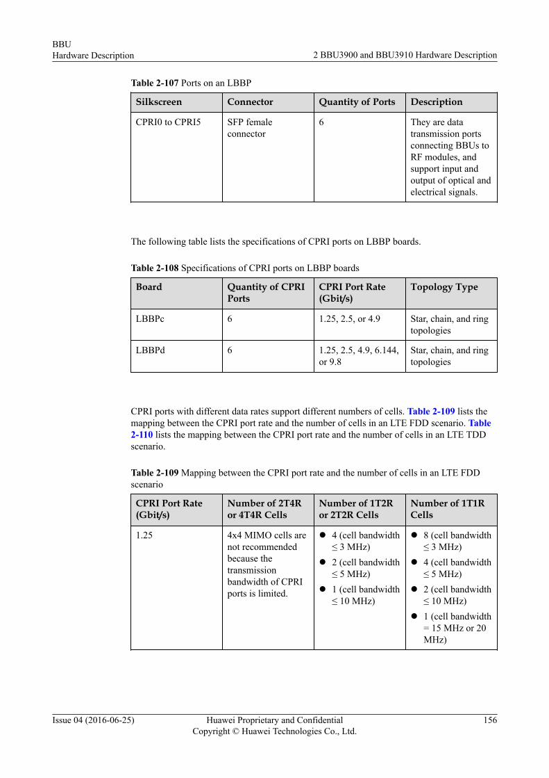
Table 2-107 Ports on an LBBP
Silkscreen Connector Quantity of Ports Description
CPRI0 to CPRI5 SFP femaleconnector
6 They are datatransmission portsconnecting BBUs toRF modules, andsupport input andoutput of optical andelectrical signals.
The following table lists the specifications of CPRI ports on LBBP boards.
Table 2-108 Specifications of CPRI ports on LBBP boards
Board Quantity of CPRIPorts
CPRI Port Rate(Gbit/s)
Topology Type
LBBPc 6 1.25, 2.5, or 4.9 Star, chain, and ringtopologies
LBBPd 6 1.25, 2.5, 4.9, 6.144,or 9.8
Star, chain, and ringtopologies
CPRI ports with different data rates support different numbers of cells. Table 2-109 lists themapping between the CPRI port rate and the number of cells in an LTE FDD scenario. Table2-110 lists the mapping between the CPRI port rate and the number of cells in an LTE TDDscenario.
Table 2-109 Mapping between the CPRI port rate and the number of cells in an LTE FDDscenario
CPRI Port Rate(Gbit/s)
Number of 2T4Ror 4T4R Cells
Number of 1T2Ror 2T2R Cells
Number of 1T1RCells
1.25 4x4 MIMO cells arenot recommendedbecause thetransmissionbandwidth of CPRIports is limited.
l 4 (cell bandwidth≤ 3 MHz)
l 2 (cell bandwidth≤ 5 MHz)
l 1 (cell bandwidth≤ 10 MHz)
l 8 (cell bandwidth≤ 3 MHz)
l 4 (cell bandwidth≤ 5 MHz)
l 2 (cell bandwidth≤ 10 MHz)
l 1 (cell bandwidth= 15 MHz or 20MHz)
BBUHardware Description 2 BBU3900 and BBU3910 Hardware Description
Issue 04 (2016-06-25) Huawei Proprietary and ConfidentialCopyright © Huawei Technologies Co., Ltd.
156
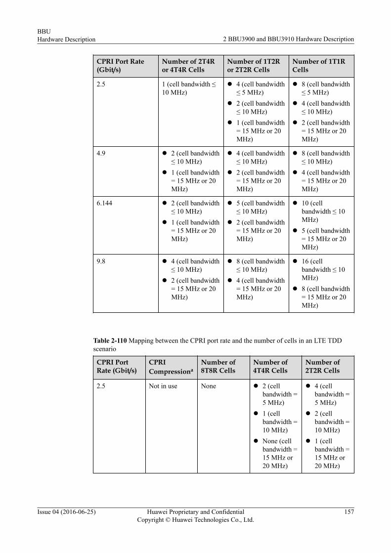
CPRI Port Rate(Gbit/s)
Number of 2T4Ror 4T4R Cells
Number of 1T2Ror 2T2R Cells
Number of 1T1RCells
2.5 1 (cell bandwidth ≤10 MHz)
l 4 (cell bandwidth≤ 5 MHz)
l 2 (cell bandwidth≤ 10 MHz)
l 1 (cell bandwidth= 15 MHz or 20MHz)
l 8 (cell bandwidth≤ 5 MHz)
l 4 (cell bandwidth≤ 10 MHz)
l 2 (cell bandwidth= 15 MHz or 20MHz)
4.9 l 2 (cell bandwidth≤ 10 MHz)
l 1 (cell bandwidth= 15 MHz or 20MHz)
l 4 (cell bandwidth≤ 10 MHz)
l 2 (cell bandwidth= 15 MHz or 20MHz)
l 8 (cell bandwidth≤ 10 MHz)
l 4 (cell bandwidth= 15 MHz or 20MHz)
6.144 l 2 (cell bandwidth≤ 10 MHz)
l 1 (cell bandwidth= 15 MHz or 20MHz)
l 5 (cell bandwidth≤ 10 MHz)
l 2 (cell bandwidth= 15 MHz or 20MHz)
l 10 (cellbandwidth ≤ 10MHz)
l 5 (cell bandwidth= 15 MHz or 20MHz)
9.8 l 4 (cell bandwidth≤ 10 MHz)
l 2 (cell bandwidth= 15 MHz or 20MHz)
l 8 (cell bandwidth≤ 10 MHz)
l 4 (cell bandwidth= 15 MHz or 20MHz)
l 16 (cellbandwidth ≤ 10MHz)
l 8 (cell bandwidth= 15 MHz or 20MHz)
Table 2-110 Mapping between the CPRI port rate and the number of cells in an LTE TDDscenario
CPRI PortRate (Gbit/s)
CPRICompressiona
Number of8T8R Cells
Number of4T4R Cells
Number of2T2R Cells
2.5 Not in use None l 2 (cellbandwidth =5 MHz)
l 1 (cellbandwidth =10 MHz)
l None (cellbandwidth =15 MHz or20 MHz)
l 4 (cellbandwidth =5 MHz)
l 2 (cellbandwidth =10 MHz)
l 1 (cellbandwidth =15 MHz or20 MHz)
BBUHardware Description 2 BBU3900 and BBU3910 Hardware Description
Issue 04 (2016-06-25) Huawei Proprietary and ConfidentialCopyright © Huawei Technologies Co., Ltd.
157

CPRI PortRate (Gbit/s)
CPRICompressiona
Number of8T8R Cells
Number of4T4R Cells
Number of2T2R Cells
In use None l None (cellbandwidth =5 MHz)
l 1 (cellbandwidth =10 MHz)
l 1 (cellbandwidth =15 MHz or20 MHz)
l None (cellbandwidth =5 MHz)
l 3 (cellbandwidth =10 MHz)
l 2 (cellbandwidth =15 MHz or20 MHz)
4.9 Not in use l None (cellbandwidth =5 MHz)
l 1 (cellbandwidth =10 MHz)
l None (cellbandwidth =15 MHz or20 MHz)
l 4 (cellbandwidth =5 MHz)
l 2 (cellbandwidth =10 MHz)
l 1 (cellbandwidth =15 MHz or20 MHz)
l 8 (cellbandwidth =5 MHz)
l 4 (cellbandwidth =10 MHz)
l 2 (cellbandwidth =15 MHz or20 MHz)
In use l None (cellbandwidth =5 MHz)
l 1 (cellbandwidth =10 MHz)
l 1 (cellbandwidth =15 MHz or20 MHz)
l None (cellbandwidth =5 MHz)
l 3 (cellbandwidth =10 MHz)
l 2 (cellbandwidth =15 MHz or20 MHz)
l None (cellbandwidth =5 MHz)
l 6 (cellbandwidth =10 MHz)
l 4 (cellbandwidth =15 MHz or20 MHz)
9.8 Not in use l None (cellbandwidth =5 MHz)
l 2 (cellbandwidth =10 MHz)
l 1 (cellbandwidth =15 MHz or20 MHz)
l 8 (cellbandwidth =5 MHz)
l 4 (cellbandwidth =10 MHz)
l 2 (cellbandwidth =15 MHz or20 MHz)
l 16 (cellbandwidth =5 MHz)
l 8 (cellbandwidth =10 MHz)
l 4 (cellbandwidth =15 MHz or20 MHz)
BBUHardware Description 2 BBU3900 and BBU3910 Hardware Description
Issue 04 (2016-06-25) Huawei Proprietary and ConfidentialCopyright © Huawei Technologies Co., Ltd.
158
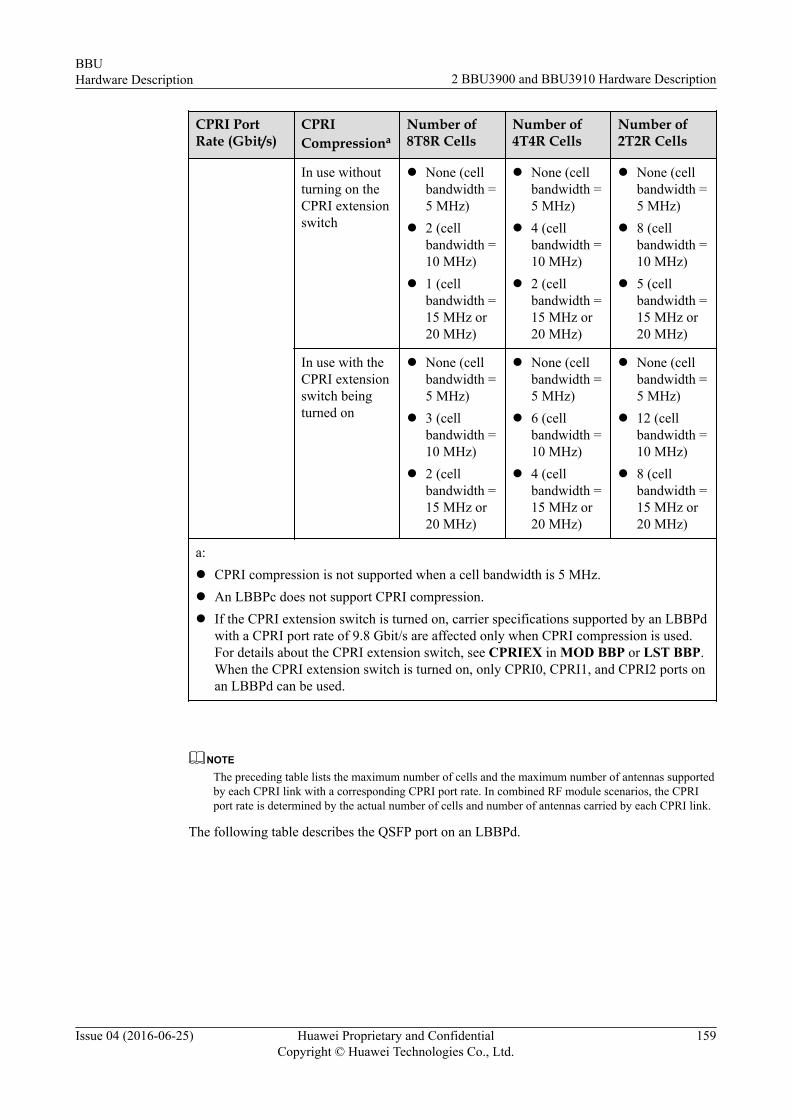
CPRI PortRate (Gbit/s)
CPRICompressiona
Number of8T8R Cells
Number of4T4R Cells
Number of2T2R Cells
In use withoutturning on theCPRI extensionswitch
l None (cellbandwidth =5 MHz)
l 2 (cellbandwidth =10 MHz)
l 1 (cellbandwidth =15 MHz or20 MHz)
l None (cellbandwidth =5 MHz)
l 4 (cellbandwidth =10 MHz)
l 2 (cellbandwidth =15 MHz or20 MHz)
l None (cellbandwidth =5 MHz)
l 8 (cellbandwidth =10 MHz)
l 5 (cellbandwidth =15 MHz or20 MHz)
In use with theCPRI extensionswitch beingturned on
l None (cellbandwidth =5 MHz)
l 3 (cellbandwidth =10 MHz)
l 2 (cellbandwidth =15 MHz or20 MHz)
l None (cellbandwidth =5 MHz)
l 6 (cellbandwidth =10 MHz)
l 4 (cellbandwidth =15 MHz or20 MHz)
l None (cellbandwidth =5 MHz)
l 12 (cellbandwidth =10 MHz)
l 8 (cellbandwidth =15 MHz or20 MHz)
a:l CPRI compression is not supported when a cell bandwidth is 5 MHz.l An LBBPc does not support CPRI compression.l If the CPRI extension switch is turned on, carrier specifications supported by an LBBPd
with a CPRI port rate of 9.8 Gbit/s are affected only when CPRI compression is used.For details about the CPRI extension switch, see CPRIEX in MOD BBP or LST BBP.When the CPRI extension switch is turned on, only CPRI0, CPRI1, and CPRI2 ports onan LBBPd can be used.
NOTEThe preceding table lists the maximum number of cells and the maximum number of antennas supportedby each CPRI link with a corresponding CPRI port rate. In combined RF module scenarios, the CPRIport rate is determined by the actual number of cells and number of antennas carried by each CPRI link.
The following table describes the QSFP port on an LBBPd.
BBUHardware Description 2 BBU3900 and BBU3910 Hardware Description
Issue 04 (2016-06-25) Huawei Proprietary and ConfidentialCopyright © Huawei Technologies Co., Ltd.
159
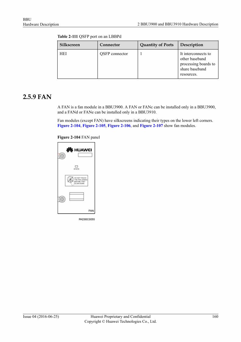
Table 2-111 QSFP port on an LBBPd
Silkscreen Connector Quantity of Ports Description
HEI QSFP connector 1 It interconnects toother basebandprocessing boards toshare basebandresources.
2.5.9 FANA FAN is a fan module in a BBU3900. A FAN or FANc can be installed only in a BBU3900,and a FANd or FANe can be installed only in a BBU3910.
Fan modules (except FAN) have silkscreens indicating their types on the lower left corners.Figure 2-104, Figure 2-105, Figure 2-106, and Figure 2-107 show fan modules.
Figure 2-104 FAN panel
BBUHardware Description 2 BBU3900 and BBU3910 Hardware Description
Issue 04 (2016-06-25) Huawei Proprietary and ConfidentialCopyright © Huawei Technologies Co., Ltd.
160
Figure 2-105 FANc panel
Figure 2-106 FANd panel
BBUHardware Description 2 BBU3900 and BBU3910 Hardware Description
Issue 04 (2016-06-25) Huawei Proprietary and ConfidentialCopyright © Huawei Technologies Co., Ltd.
161
Figure 2-107 FANe panel
FunctionA FAN performs the following functions:l It dissipates heat from other boards in the BBU.l It controls the speed of fans, monitors the temperature of fans, and reports the status,
temperature and in-position signals of fans.l A FANc, FANd, or FANe provides a read/write electronic label.
2.5.10 UPEUA UPEU is a universal power and environment interface unit. A UPEUd can be installed in aBBU3900 and a UPEUa, UPEUb or UPEUc can be installed only in a BBU3900.
Figure 2-108, Figure 2-109, Figure 2-110, and Figure 2-111 show the four types of UPEUboards.
NOTE
l A UPEUc and a UPEUd have silkscreens UPEUc and UPEUd indicating their board types on them,whereas a UPEUa and a UPEUb do not have such silkscreens indicating their board types. A UPEUaand a UPEUb, however, can be distinguished by silkscreens -48V and +24V on them.
l The silkscreen above a power port is in the "A, B" format. A indicates the rated voltage, and Bindicates the rated current. For example, "-48V, 8A".
BBUHardware Description 2 BBU3900 and BBU3910 Hardware Description
Issue 04 (2016-06-25) Huawei Proprietary and ConfidentialCopyright © Huawei Technologies Co., Ltd.
162

Figure 2-108 UPEUa panel
(1) BBU power switch (2) 7W2 connector
Figure 2-109 UPEUb panel
(1) BBU power switch (2) 7W2 connector
Figure 2-110 UPEUc panel
(1) BBU power switch (2) 3V3 connector
BBUHardware Description 2 BBU3900 and BBU3910 Hardware Description
Issue 04 (2016-06-25) Huawei Proprietary and ConfidentialCopyright © Huawei Technologies Co., Ltd.
163

Figure 2-111 UPEUd panel
(1) BBU power switch (2) 3V3 connector
SpecificationsThe following table lists the specifications of a UPEUa, a UPEUc, and a UPEUd.
Table 2-112 Specifications of UPEU boards
Board Output Power (W)
One UPEU Two UPEU Boards(in CurrentEqualization Mode)
Two UPEU Boards(1+1 RedundancyBackup Mode)
UPEUa 300 - 300
UPEUb 250 - 250
UPEUc 360 650 360
UPEUd 650 - 650
NOTE
l 1+1 redundancy backup mode: When power required by a BBU does not exceed power provided bya single UPEU, two UPEUs automatically work in 1+1 backup mode and only one UPEU is workingat a time.
l Current equalization mode: Only UPEUc boards support this mode. When power required by a BBUexceeds the maximum power provided by a single UPEUc, both UPEUc boards provide power.
l A BBU cannot house two UPEU boards of different types. When power required by a BBU exceedspower specifications of the BBU:l If the BBU has been configured with one or two UPEUa boards, replace the boards with two
UPEUc boards.l If the BBU has been configured with one UPEUc board, add a UPEUc board.
l If two UPEUc boards are configured, output power is large and therefore a FANc must beconfigured.
FunctionUPEU boards perform the following functions:
BBUHardware Description 2 BBU3900 and BBU3910 Hardware Description
Issue 04 (2016-06-25) Huawei Proprietary and ConfidentialCopyright © Huawei Technologies Co., Ltd.
164
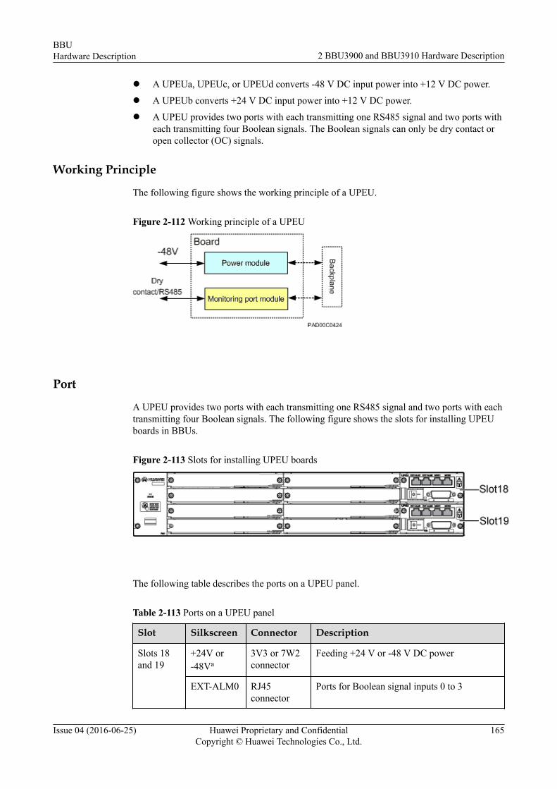
l A UPEUa, UPEUc, or UPEUd converts -48 V DC input power into +12 V DC power.
l A UPEUb converts +24 V DC input power into +12 V DC power.
l A UPEU provides two ports with each transmitting one RS485 signal and two ports witheach transmitting four Boolean signals. The Boolean signals can only be dry contact oropen collector (OC) signals.
Working Principle
The following figure shows the working principle of a UPEU.
Figure 2-112 Working principle of a UPEU
Port
A UPEU provides two ports with each transmitting one RS485 signal and two ports with eachtransmitting four Boolean signals. The following figure shows the slots for installing UPEUboards in BBUs.
Figure 2-113 Slots for installing UPEU boards
The following table describes the ports on a UPEU panel.
Table 2-113 Ports on a UPEU panel
Slot Silkscreen Connector Description
Slots 18and 19
+24V or-48Va
3V3 or 7W2connector
Feeding +24 V or -48 V DC power
EXT-ALM0 RJ45connector
Ports for Boolean signal inputs 0 to 3
BBUHardware Description 2 BBU3900 and BBU3910 Hardware Description
Issue 04 (2016-06-25) Huawei Proprietary and ConfidentialCopyright © Huawei Technologies Co., Ltd.
165
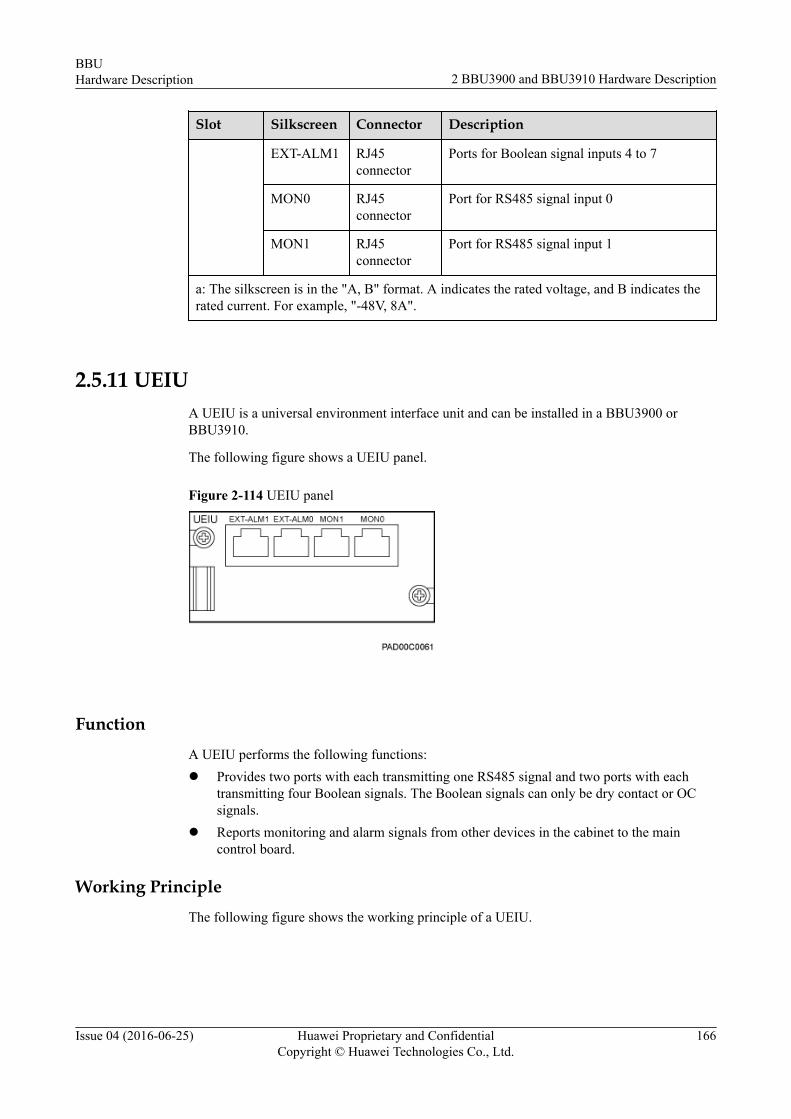
Slot Silkscreen Connector Description
EXT-ALM1 RJ45connector
Ports for Boolean signal inputs 4 to 7
MON0 RJ45connector
Port for RS485 signal input 0
MON1 RJ45connector
Port for RS485 signal input 1
a: The silkscreen is in the "A, B" format. A indicates the rated voltage, and B indicates therated current. For example, "-48V, 8A".
2.5.11 UEIUA UEIU is a universal environment interface unit and can be installed in a BBU3900 orBBU3910.
The following figure shows a UEIU panel.
Figure 2-114 UEIU panel
FunctionA UEIU performs the following functions:l Provides two ports with each transmitting one RS485 signal and two ports with each
transmitting four Boolean signals. The Boolean signals can only be dry contact or OCsignals.
l Reports monitoring and alarm signals from other devices in the cabinet to the maincontrol board.
Working PrincipleThe following figure shows the working principle of a UEIU.
BBUHardware Description 2 BBU3900 and BBU3910 Hardware Description
Issue 04 (2016-06-25) Huawei Proprietary and ConfidentialCopyright © Huawei Technologies Co., Ltd.
166
Figure 2-115 Working principle of a UEIU
Port
The following table describes the ports on a UEIU panel.
Table 2-114 Ports on a UEIU panel
Silkscreen
Connector
Quantity ofPorts
Description
EXT-ALM0
RJ45connector
1 Ports for Boolean signal inputs 0 to 3
EXT-ALM1
RJ45connector
1 Ports for Boolean signal inputs 4 to 7
MON0 RJ45connector
1 Port for RS485 signal input 0
MON1 RJ45connector
1 Port for RS485 signal input 1
2.5.12 UTRPA UTRP is a universal transmission processing unit. A UTRPa or UTRPc can be configuredin a BBU3900 or BBU3910. Other types of UTRP boards can be configured only in aBBU3900.
The following figure shows a UTRP2 panel.
Figure 2-116 UTRP2 panel (with two optical ports)
The following figure shows a UTRP3 or UTRP4 panel.
BBUHardware Description 2 BBU3900 and BBU3910 Hardware Description
Issue 04 (2016-06-25) Huawei Proprietary and ConfidentialCopyright © Huawei Technologies Co., Ltd.
167

Figure 2-117 UTRP3 or UTRP4 panel (with eight E1/T1 channels)
The following figure shows a UTRPb4 panel in GSM mode.
Figure 2-118 UTRPb4 panel (with eight E1/T1 channels)
The following figure shows a UTRP6 panel.
Figure 2-119 UTRP6 panel (with one STM-1 channel)
The following figure shows a UTRP9 panel.
Figure 2-120 UTRP9 panel (with four electrical ports)
The following figure shows a UTRPa panel.
Figure 2-121 UTRPa panel (with eight E1/T1 channels)
BBUHardware Description 2 BBU3900 and BBU3910 Hardware Description
Issue 04 (2016-06-25) Huawei Proprietary and ConfidentialCopyright © Huawei Technologies Co., Ltd.
168

The following figure shows a UTRPc panel.
Figure 2-122 UTRPc panel (with four electrical ports and two optical ports)
Specifications
The following table lists the specifications of UTRP boards.
Table 2-115 Specifications of UTRP boards
Board Sub-board/BoardType
Applicable Mode
TransmissionMode
Quantityof Ports
PortCapacity
Full/Half-Duplex
UTRP2 UEOC UMTS Transmission overFE/GEopticalports
2 10 Mbit/s,100Mbit/s, or1000Mbit/s
Full-duplex
UTRP3 UAEC UMTS ATM overE1/T1
2 Eightchannels
Full-duplex
UTRP4 UIEC UMTS IP overE1/T1
2 Eightchannels
Full-duplex
UTRPb4 Without asub-board
GSM TDM overE1/T1
2 Eightchannels
Full-duplex
UTRP6 UUAS UMTS STM-1/OC-3
1 Onechannel
Full-duplex
UTRP9 UQEC UMTS Transmission overFE/GEelectricalports
4 10 Mbit/s,100Mbit/s, or1000Mbit/s
Full-duplex
UTRPa Without asub-board
UMTS ATM overE1/T1 orIP overE1/T1
2 Eightchannels
Full-duplex
BBUHardware Description 2 BBU3900 and BBU3910 Hardware Description
Issue 04 (2016-06-25) Huawei Proprietary and ConfidentialCopyright © Huawei Technologies Co., Ltd.
169

Board Sub-board/BoardType
Applicable Mode
TransmissionMode
Quantityof Ports
PortCapacity
Full/Half-Duplex
UTRPc Without asub-board
UMTSCo-transmission used bymultiplemodesincludingUMTS(mastermode on aUTRPc)
Transmission overFE/GEelectricalports
4 10 Mbit/s,100Mbit/s, or1000Mbit/s
Full-duplex
Transmission overFE/GEopticalports
2 100 Mbit/sor 1000Mbit/s
Full-duplex
NOTE
For the signaling specifications of a UTRP working in UMTS mode, see section "TechnicalSpecifications of the BBU3900s and BBU3910s" in 3900 Series Base Station Technical Description.
Function
A UTRP performs the following functions:l Provides E1/T1 transmission port over ATM, TDM or IP.l Provides electrical and optical transmission ports.l Supports cold backup.
Working Principle
The following figure shows the working principle of a UTRP.
Figure 2-123 Working principle of a UTRP
Port
The following table describes the ports on a UTRP panel.
BBUHardware Description 2 BBU3900 and BBU3910 Hardware Description
Issue 04 (2016-06-25) Huawei Proprietary and ConfidentialCopyright © Huawei Technologies Co., Ltd.
170

Table 2-116 Ports on a UTRP panel
Board Silkscreen Connector Description
UTRP2 FE/GE0 andFE/GE1
SFP femaleconnector
FE/GE optical signaltransmission port
UTRP3, UTRP4,UTRPb4, or UTRPa
E1/T1 DB26 femaleconnector
E1/T1 signaltransmission port
UTRP6 STM-1/OC-3 SFP femaleconnector
STM-1/OC-3 signaltransmission port
UTRP9 FE/GE0 to FE/GE3 RJ45 connector FE/GE electricalsignal transmissionport
UTRPc FE/GE0 andFE/GE1
SFP femaleconnector
FE/GE optical signaltransmission port
FE/GE2 to FE/GE5 RJ45 connector FE/GE electricalsignal transmissionport
DIP SwitchThere are three DIP switches on a UTRP3, UTRP4, or UTRPb4, and there are two DIPswitches on a UTRPa. Figure 2-124 shows the DIP switches on a UTRP3 or UTRP4. Figure2-125 shows the DIP switches on a UTRPb4. Figure 2-126 shows the DIP switches on aUTRPa.
Figure 2-124 DIP switches on a UTRP3 or UTRP4
BBUHardware Description 2 BBU3900 and BBU3910 Hardware Description
Issue 04 (2016-06-25) Huawei Proprietary and ConfidentialCopyright © Huawei Technologies Co., Ltd.
171

Figure 2-125 DIP switches on a UTRPb4
Figure 2-126 DIP switches on a UTRPa
The DIP switches perform the following functions:
l SW1 and SW2 are used to set whether to ground the receiver end of the E1.
l SW3 is used to set the resistance of the E1 signals.
Each DIP switch has four bits. Table 2-117, Table 2-118, and Table 2-119 describe the bitsettings and meanings of the DIP switches.
Table 2-117 DIP switch SW1
DIPSwitch
Bit Setting Description
1 2 3 4
SW1 OFF OFF OFF OFF Balanced
ON ON ON ON Unbalanced
BBUHardware Description 2 BBU3900 and BBU3910 Hardware Description
Issue 04 (2016-06-25) Huawei Proprietary and ConfidentialCopyright © Huawei Technologies Co., Ltd.
172
DIPSwitch
Bit Setting Description
1 2 3 4
Miscellaneous Unavailable
Table 2-118 DIP switch SW2
DIPSwitch
Bit Setting Description
1 2 3 4
SW2 OFF OFF OFF OFF Balanced
ON ON ON ON Unbalanced
Miscellaneous Unavailable
NOTICESW1 and SW2 are set to OFF by default. SW1 corresponds to No.4 to No.7 E1 channels.SW2 corresponds to No.0 to No.3 E1 channels.
Table 2-119 DIP switch SW3
DIPSwitch
Bit Setting Description
1 2 3 4
SW3 OFF OFF ON ON T1
ON ON OFF OFF The E1resistance isset to 120ohms.
ON ON ON ON The E1resistance isset to 75ohms.
Miscellaneous Unavailable
2.5.13 USCUA USCU is a universal satellite card and clock unit and can be installed in a BBU3900 orBBU3910.
BBUHardware Description 2 BBU3900 and BBU3910 Hardware Description
Issue 04 (2016-06-25) Huawei Proprietary and ConfidentialCopyright © Huawei Technologies Co., Ltd.
173

USCU boards have two types of exteriors, which are shown in Figure 2-127 and Figure2-128.
NOTEA USCUb11 and a USCUb14 have labels USCUb11 and USCUb14 indicating their board types on thelower left corners, respectively.
Figure 2-127 USCUb11 or USCUb14 panel
Figure 2-128 USCUb22 panel
Specifications
The following table describes specifications of the three types of USCU boards.
Table 2-120 Specifications of USCU boards
Board Working Mode Supported Satellite Card
USCUb11 LTE None
USCUb14 GSMUMTSLTE
UBLOX single-satellite card
USCUb22 GSMUMTSLTE
Naviors dual-satellite card
BBUHardware Description 2 BBU3900 and BBU3910 Hardware Description
Issue 04 (2016-06-25) Huawei Proprietary and ConfidentialCopyright © Huawei Technologies Co., Ltd.
174

Function
USCU boards perform the following functions:
l A USCUb11 provides ports for communicating with the RGPS (for example, the RGPSon the reused customer equipment) and BITS equipment. It does not support GPSsignals.
l A USCUb14 does not support RGPS signals. It contains a UBLOX satellite card.
l A USCUb22 does not support RGPS signals. It uses a Naviors satellite card, which mustbe purchased locally and installed onsite.
Working Principle
The following figure shows the working principle of a USCU.
Figure 2-129 Working principle of a USCU
Port
The following table describes the ports on a USCU panel.
Table 2-121 Ports on a USCU panel
Silkscreen Connector Description
GPS SMA connector The GPS ports on a USCUb14 or USCUb22 areused for receiving GPS signals.The GPS port on a USCUb11 is reserved, and itcannot receive GPS signals.
RGPS PCB weldedwiring terminal
The RGPS port on a USCUb11 is used forreceiving RGPS signals.The RGPS ports on a USCUb14 or USCUb22 arereserved, and they cannot receive RGPS signals.
TOD0 RJ45 connector Receives or transmits 1PPS+TOD signals.
TOD1 RJ45 connector Receives or transmits 1PPS+TOD signals, andreceives TOD signals from the M1000.
BBUHardware Description 2 BBU3900 and BBU3910 Hardware Description
Issue 04 (2016-06-25) Huawei Proprietary and ConfidentialCopyright © Huawei Technologies Co., Ltd.
175
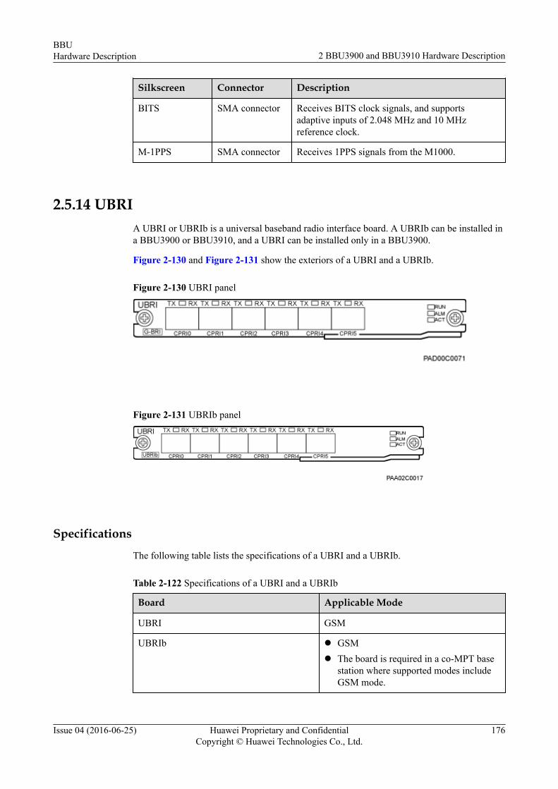
Silkscreen Connector Description
BITS SMA connector Receives BITS clock signals, and supportsadaptive inputs of 2.048 MHz and 10 MHzreference clock.
M-1PPS SMA connector Receives 1PPS signals from the M1000.
2.5.14 UBRIA UBRI or UBRIb is a universal baseband radio interface board. A UBRIb can be installed ina BBU3900 or BBU3910, and a UBRI can be installed only in a BBU3900.
Figure 2-130 and Figure 2-131 show the exteriors of a UBRI and a UBRIb.
Figure 2-130 UBRI panel
Figure 2-131 UBRIb panel
Specifications
The following table lists the specifications of a UBRI and a UBRIb.
Table 2-122 Specifications of a UBRI and a UBRIb
Board Applicable Mode
UBRI GSM
UBRIb l GSMl The board is required in a co-MPT base
station where supported modes includeGSM mode.
BBUHardware Description 2 BBU3900 and BBU3910 Hardware Description
Issue 04 (2016-06-25) Huawei Proprietary and ConfidentialCopyright © Huawei Technologies Co., Ltd.
176

FunctionA UBRI or UBRIb performs the following functions:l A UBRI or UBRIb provides extended CPRI optical or electrical ports.l When a UBRI or UBRIb is working in GSM mode, RF modules process baseband
signals.l A UBRIb receives CPRI signals in a single-mode or multimode base station.l A UBRIb only supports single mode in a separate-MPT base station.
Working PrincipleThe following figure shows the working principle of a UBRI or UBRIb.
Figure 2-132 Working principle of a UBRI or UBRIb
PortThe following table describes the ports on a UBRI or UBRIb.
Table 2-123 Ports on a UBRI or UBRIb
Silkscreen Connector Description
CPRI0 to CPRI5 SFP female connector Connects a BBU to RFmodules.
The following table lists specifications of the CPRI ports on a UBRI and a UBRIb.
BBUHardware Description 2 BBU3900 and BBU3910 Hardware Description
Issue 04 (2016-06-25) Huawei Proprietary and ConfidentialCopyright © Huawei Technologies Co., Ltd.
177
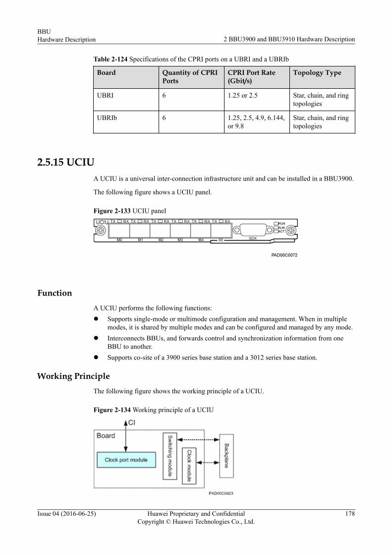
Table 2-124 Specifications of the CPRI ports on a UBRI and a UBRIb
Board Quantity of CPRIPorts
CPRI Port Rate(Gbit/s)
Topology Type
UBRI 6 1.25 or 2.5 Star, chain, and ringtopologies
UBRIb 6 1.25, 2.5, 4.9, 6.144,or 9.8
Star, chain, and ringtopologies
2.5.15 UCIUA UCIU is a universal inter-connection infrastructure unit and can be installed in a BBU3900.
The following figure shows a UCIU panel.
Figure 2-133 UCIU panel
FunctionA UCIU performs the following functions:l Supports single-mode or multimode configuration and management. When in multiple
modes, it is shared by multiple modes and can be configured and managed by any mode.l Interconnects BBUs, and forwards control and synchronization information from one
BBU to another.l Supports co-site of a 3900 series base station and a 3012 series base station.
Working PrincipleThe following figure shows the working principle of a UCIU.
Figure 2-134 Working principle of a UCIU
BBUHardware Description 2 BBU3900 and BBU3910 Hardware Description
Issue 04 (2016-06-25) Huawei Proprietary and ConfidentialCopyright © Huawei Technologies Co., Ltd.
178
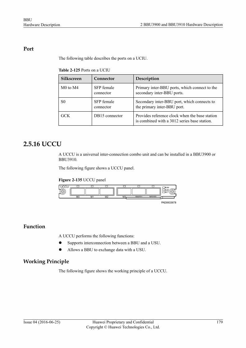
PortThe following table describes the ports on a UCIU.
Table 2-125 Ports on a UCIU
Silkscreen Connector Description
M0 to M4 SFP femaleconnector
Primary inter-BBU ports, which connect to thesecondary inter-BBU ports.
S0 SFP femaleconnector
Secondary inter-BBU port, which connects tothe primary inter-BBU port.
GCK DB15 connector Provides reference clock when the base stationis combined with a 3012 series base station.
2.5.16 UCCUA UCCU is a universal inter-connection combo unit and can be installed in a BBU3900 orBBU3910.
The following figure shows a UCCU panel.
Figure 2-135 UCCU panel
FunctionA UCCU performs the following functions:l Supports interconnection between a BBU and a USU.l Allows a BBU to exchange data with a USU.
Working PrincipleThe following figure shows the working principle of a UCCU.
BBUHardware Description 2 BBU3900 and BBU3910 Hardware Description
Issue 04 (2016-06-25) Huawei Proprietary and ConfidentialCopyright © Huawei Technologies Co., Ltd.
179

Figure 2-136 Working principle of a UCCU
PortThe following table describes the ports on a UCCU.
Table 2-126 Ports on the UCCU
Silkscreen Connector Description
M0 to M3 QSFP connector Primary interconnectionports, which can beconnected to HEI ports onthe baseband processingboard in a BBU
M4/S1
M5/S0 QSFP connector Secondary interconnectionport, which can beconnected to any of thefollowing remote ports:l HEI port on the ULPU in
a USU3910l M5/S0 port on the
UCCU in another BBU
2.5.17 Optical ModulesAn optical module transmits optical signals between an optical port and a fiber optic cable.
BBUHardware Description 2 BBU3900 and BBU3910 Hardware Description
Issue 04 (2016-06-25) Huawei Proprietary and ConfidentialCopyright © Huawei Technologies Co., Ltd.
180
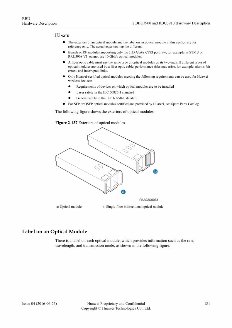
NOTE
l The exteriors of an optical module and the label on an optical module in this section are forreference only. The actual exteriors may be different.
l Boards or RF modules supporting only the 1.25 Gbit/s CPRI port rate, for example, a GTMU orRRU3908 V1, cannot use 10 Gbit/s optical modules.
l A fiber optic cable must use the same type of optical modules on its two ends. If different types ofoptical modules are used by a fiber optic cable, performance risks may arise, for example, alarms, biterrors, and interrupted links.
l Only Huawei-certified optical modules meeting the following requirements can be used for Huaweiwireless devices:
l Requirements of devices on which optical modules are to be installed
l Laser safety in the IEC 60825-1 standard
l General safety in the IEC 60950-1 standard
l For SFP or QSFP optical modules certified and provided by Huawei, see Spare Parts Catalog.
The following figure shows the exteriors of optical modules.
Figure 2-137 Exteriors of optical modules
a: Optical module b: Single-fiber bidirectional optical module
Label on an Optical ModuleThere is a label on each optical module, which provides information such as the rate,wavelength, and transmission mode, as shown in the following figure.
BBUHardware Description 2 BBU3900 and BBU3910 Hardware Description
Issue 04 (2016-06-25) Huawei Proprietary and ConfidentialCopyright © Huawei Technologies Co., Ltd.
181

Figure 2-138 Label on an optical module
(1) Rate (2) Wavelength (3) Transmission mode
Optical Module TypeOptical modules can be divided into single- and multimode optical modules, which can bedistinguished as follows:l The puller of a single-mode optical module is blue and the puller of a multimode optical
module is black or gray.l The transmission mode is displayed as "SM" on the label of a single-mode optical
module and "MM" on the label of a multimode optical module.
2.6 Indicators on BBU BoardsThis chapter describes the indicators on BBU boards.
2.6.1 Status IndicatorsThis section describes the indicators showing the running status of BBU boards.
The following figure shows the indicator status on BBU boards. The following table describesthe meanings of the indicators.
BBUHardware Description 2 BBU3900 and BBU3910 Hardware Description
Issue 04 (2016-06-25) Huawei Proprietary and ConfidentialCopyright © Huawei Technologies Co., Ltd.
182
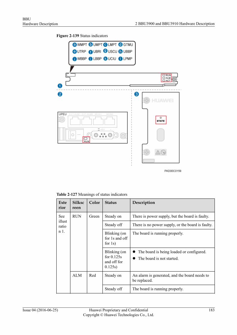
Figure 2-139 Status indicators
Table 2-127 Meanings of status indicators
Exterior
Silkscreen
Color Status Description
Seeillustration 1.
RUN Green Steady on There is power supply, but the board is faulty.
Steady off There is no power supply, or the board is faulty.
Blinking (onfor 1s and offfor 1s)
The board is running properly.
Blinking (onfor 0.125sand off for0.125s)
l The board is being loaded or configured.l The board is not started.
ALM Red Steady on An alarm is generated, and the board needs tobe replaced.
Steady off The board is running properly.
BBUHardware Description 2 BBU3900 and BBU3910 Hardware Description
Issue 04 (2016-06-25) Huawei Proprietary and ConfidentialCopyright © Huawei Technologies Co., Ltd.
183

Exterior
Silkscreen
Color Status Description
Blinking (onfor 1s and offfor 1s)
An alarm is generated, and you need to locatethe fault before determining whether to replacethe board.
ACT Green Steady on l Main control board: The board is serving asan active board.
l UTRP working in GSM mode:– Before the configuration takes effect,
none or more than one E1 port in GSMmode are functional.
– The configuration has taken effect.l Boards other than main control boards: The
boards have been activated and areproviding services.
Steady off l Main control board: The board is notserving as an active board.
l Boards other than main control boards: Theboards have not been activated or are notproviding services.
Blinking (onfor 0.125sand off for0.125s)
l Main control board: The operation andmaintenance link (OML) is disconnected.
l UTRP working in GSM mode: Before theconfiguration takes effect, only one E1 portin GSM mode is functional.
l Boards other than main control boards: N/A
Blinking (onfor 1s and offfor 1s)
l UMPT supporting the UMTS single modeor UMPT deployed with multiple modesincluding UMTS: The board is being tested,for example, going through an RF modulevoltage standing wave ratio (VSWR) test byusing a USB flash drivea.
l WBBPf, LBBPd, or UBRIb: The powersupply for this board is insufficient.
l Other boards: N/A
Blinking (Inevery 4s, theindicator ison for 0.125sand off for0.125s [eighttimes] in thefirst 2s andthen off for2s.)
l UMPT supporting the LTE single mode orUMPT deployed with multiple modesincluding LTE:– All cells configured for the subrack that
houses this board are not activated.– The S1 link is faulty.
l Other boards: N/A
BBUHardware Description 2 BBU3900 and BBU3910 Hardware Description
Issue 04 (2016-06-25) Huawei Proprietary and ConfidentialCopyright © Huawei Technologies Co., Ltd.
184
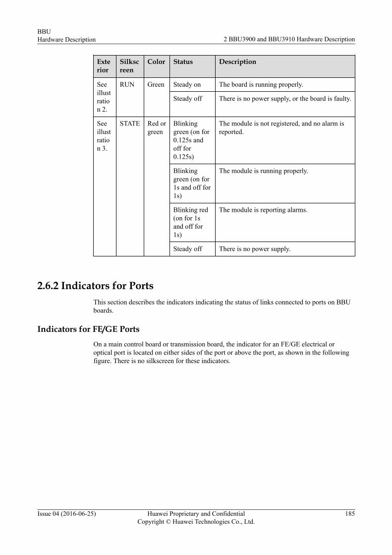
Exterior
Silkscreen
Color Status Description
Seeillustration 2.
RUN Green Steady on The board is running properly.
Steady off There is no power supply, or the board is faulty.
Seeillustration 3.
STATE Red orgreen
Blinkinggreen (on for0.125s andoff for0.125s)
The module is not registered, and no alarm isreported.
Blinkinggreen (on for1s and off for1s)
The module is running properly.
Blinking red(on for 1sand off for1s)
The module is reporting alarms.
Steady off There is no power supply.
2.6.2 Indicators for PortsThis section describes the indicators indicating the status of links connected to ports on BBUboards.
Indicators for FE/GE PortsOn a main control board or transmission board, the indicator for an FE/GE electrical oroptical port is located on either sides of the port or above the port, as shown in the followingfigure. There is no silkscreen for these indicators.
BBUHardware Description 2 BBU3900 and BBU3910 Hardware Description
Issue 04 (2016-06-25) Huawei Proprietary and ConfidentialCopyright © Huawei Technologies Co., Ltd.
185

Figure 2-140 Positions of indicators for FE/GE ports
The following table describes the indicators for FE/GE ports.
Table 2-128 Indicators for FE/GE ports
Exterior
Silkscreen
Color Status Description
Seeillustration 1.
LINK Green Steady on The connection is set up successfully.
Steady off No connection is set up.
ACT Orange Steady on Data is being transmitted or received.
Steady off No data is being transmitted or received.
Seeillustration 2 or3.
TX RX Red orgreen
Steadygreen
The Ethernet link is functioning properly.
Steady red The optical module is transmitting orreceiving faulty.
Blinkingred (on for1s and offfor 1s)
Ethernet negotiation is faulty.
BBUHardware Description 2 BBU3900 and BBU3910 Hardware Description
Issue 04 (2016-06-25) Huawei Proprietary and ConfidentialCopyright © Huawei Technologies Co., Ltd.
186
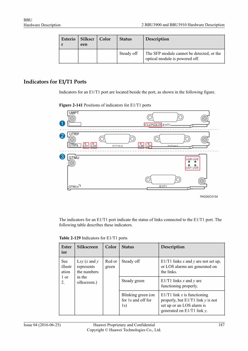
Exterior
Silkscreen
Color Status Description
Steady off The SFP module cannot be detected, or theoptical module is powered off.
Indicators for E1/T1 Ports
Indicators for an E1/T1 port are located beside the port, as shown in the following figure.
Figure 2-141 Positions of indicators for E1/T1 ports
The indicators for an E1/T1 port indicate the status of links connected to the E1/T1 port. Thefollowing table describes these indicators.
Table 2-129 Indicators for E1/T1 ports
Exterior
Silkscreen Color Status Description
Seeillustration1 or2.
Lxy (x and yrepresentsthe numbersin thesilkscreen.)
Red orgreen
Steady off E1/T1 links x and y are not set up,or LOS alarms are generated onthe links.
Steady green E1/T1 links x and y arefunctioning properly.
Blinking green (onfor 1s and off for1s)
E1/T1 link x is functioningproperly, but E1/T1 link y is notset up or an LOS alarm isgenerated on E1/T1 link y.
BBUHardware Description 2 BBU3900 and BBU3910 Hardware Description
Issue 04 (2016-06-25) Huawei Proprietary and ConfidentialCopyright © Huawei Technologies Co., Ltd.
187

Exterior
Silkscreen Color Status Description
Blinking green (onfor 0.125s and offfor 0.125s)
E1/T1 link y is functioningproperly, but E1/T1 link x is notset up or an LOS alarm isgenerated on E1/T1 link x.
Steady red Alarms are generated on E1/T1links x and y.
Blinking red (onfor 1s and off for1s)
An alarm is generated on E1/T1link x.
Blinking red (onfor 0.125s and offfor 0.125s)
An alarm is generated on E1/T1link y.
Seeillustration3.
LIU0 toLIU3
Green Steady on An E1/T1 local alarm is generated.
Blinking (on for 1sand off for 1s)
An E1/T1 remote alarm isgenerated.
Steady off The link is functioning properly.
Indicators for CPRI PortsIndicators for a CPRI port are above the ports, as shown in the following figure.
Figure 2-142 Positions of indicators for CPRI ports
The indicators for a CPRI port indicate the status of links connected to the CPRI port. Thefollowing table describes these indicators.
BBUHardware Description 2 BBU3900 and BBU3910 Hardware Description
Issue 04 (2016-06-25) Huawei Proprietary and ConfidentialCopyright © Huawei Technologies Co., Ltd.
188

Table 2-130 Indicators for CPRI ports
Silkscreen
Color Status Description
TX RX Red orgreen
Steady green The CPRI link is functioning properly.
Steady red An optical module fails to transmit or receivesignals due to one of the following causes:l The optical module is faulty.l The fiber optic cable is broken.
Blinking red (onfor 0.125s and offfor 0.125s)
The RF module connected to the CPRI port hasa hardware fault.
Blinking red (onfor 1s and off for1s)
The CPRI link is out of lock due to one of thefollowing causes:l There is no mutual lock between dual-mode
reference clocks.l The CPRI port rate does not match the rate
of the optical module.l The VSWR alarm is reported on the RF
module connected to the CPRI port when theUSB flash drivea connected to the maincontrol board is under test. (This is only forthe baseband processing board working inUMTS mode.)
Steady off l The optical module cannot be detected.l The CPRI electrical cable is not connected.
a: The security of the USB port is ensured by encryption, and the USB port can be shutdown using commands.
Indicators for Interconnection PortsIndicators for an interconnection port are either above or below the port, as shown in thefollowing figure.
BBUHardware Description 2 BBU3900 and BBU3910 Hardware Description
Issue 04 (2016-06-25) Huawei Proprietary and ConfidentialCopyright © Huawei Technologies Co., Ltd.
189

Figure 2-143 Positions of indicators for interconnection ports
The indicators for an interconnection port indicate the status of links connected to theinterconnection port. The following table describes these indicators.
Table 2-131 Indicators for interconnection ports
Exterior
Silkscreen
Color Status Description
Seeillustration1.
HEIa Red orgreen
Steady green The interconnection link isfunctioning properly.
Steady red An optical module fails to transmitor receive signals due to one of thefollowing causes:l The optical module is faulty.l The fiber optic cable is broken.
Blinking red(on for 1s andoff for 1s)
The interconnection link is out oflock due to one of the followingcauses:l Mutual locking between two
interconnected BBUs fails.l The QSFP port rate does not
match the rate of the opticalmodule.
Steady off The optical module cannot bedetected.
Seeillustration2.
CI Red orgreen
Steady green The interconnection link isfunctioning properly.
BBUHardware Description 2 BBU3900 and BBU3910 Hardware Description
Issue 04 (2016-06-25) Huawei Proprietary and ConfidentialCopyright © Huawei Technologies Co., Ltd.
190
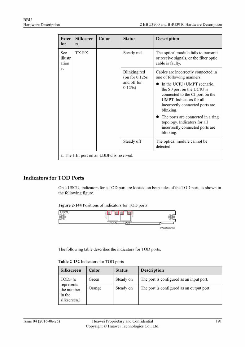
Exterior
Silkscreen
Color Status Description
Seeillustration3.
TX RX Steady red The optical module fails to transmitor receive signals, or the fiber opticcable is faulty.
Blinking red(on for 0.125sand off for0.125s)
Cables are incorrectly connected inone of following manners:l In the UCIU+UMPT scenario,
the S0 port on the UCIU isconnected to the CI port on theUMPT. Indicators for allincorrectly connected ports areblinking.
l The ports are connected in a ringtopology. Indicators for allincorrectly connected ports areblinking.
Steady off The optical module cannot bedetected.
a: The HEI port on an LBBPd is reserved.
Indicators for TOD Ports
On a USCU, indicators for a TOD port are located on both sides of the TOD port, as shown inthe following figure.
Figure 2-144 Positions of indicators for TOD ports
The following table describes the indicators for TOD ports.
Table 2-132 Indicators for TOD ports
Silkscreen Color Status Description
TODn (nrepresentsthe numberin thesilkscreen.)
Green Steady on The port is configured as an input port.
Orange Steady on The port is configured as an output port.
BBUHardware Description 2 BBU3900 and BBU3910 Hardware Description
Issue 04 (2016-06-25) Huawei Proprietary and ConfidentialCopyright © Huawei Technologies Co., Ltd.
191
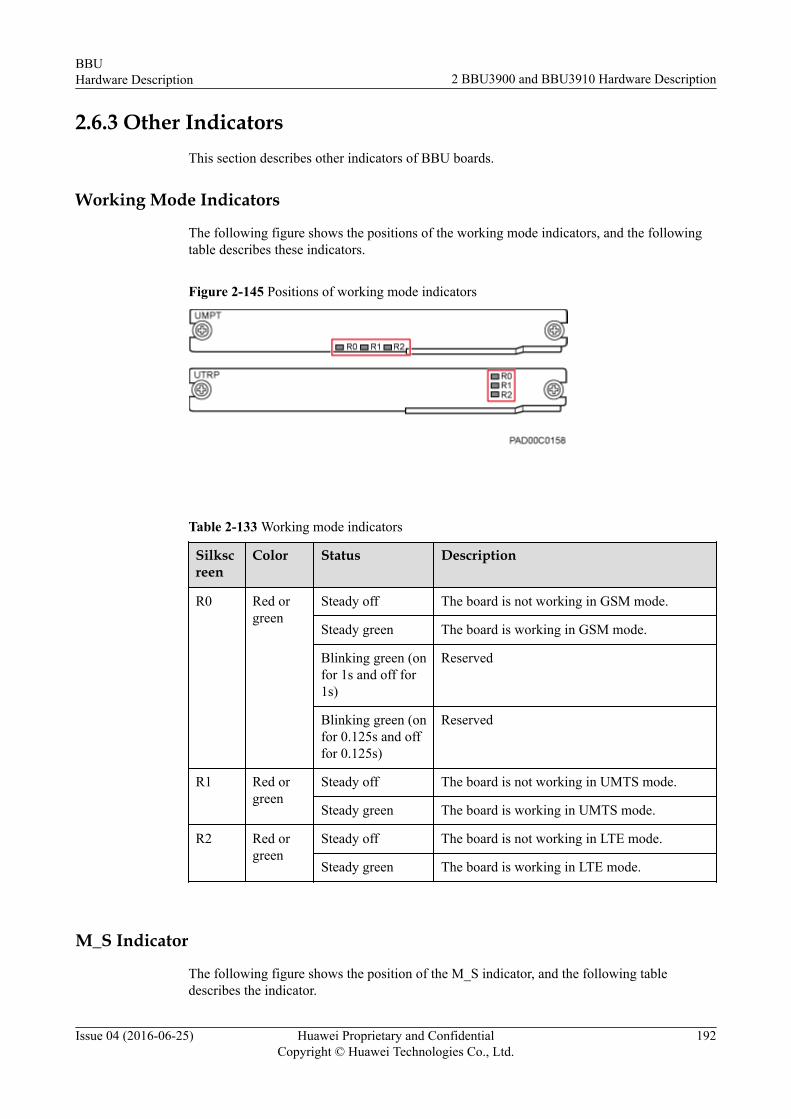
2.6.3 Other IndicatorsThis section describes other indicators of BBU boards.
Working Mode Indicators
The following figure shows the positions of the working mode indicators, and the followingtable describes these indicators.
Figure 2-145 Positions of working mode indicators
Table 2-133 Working mode indicators
Silkscreen
Color Status Description
R0 Red orgreen
Steady off The board is not working in GSM mode.
Steady green The board is working in GSM mode.
Blinking green (onfor 1s and off for1s)
Reserved
Blinking green (onfor 0.125s and offfor 0.125s)
Reserved
R1 Red orgreen
Steady off The board is not working in UMTS mode.
Steady green The board is working in UMTS mode.
R2 Red orgreen
Steady off The board is not working in LTE mode.
Steady green The board is working in LTE mode.
M_S Indicator
The following figure shows the position of the M_S indicator, and the following tabledescribes the indicator.
BBUHardware Description 2 BBU3900 and BBU3910 Hardware Description
Issue 04 (2016-06-25) Huawei Proprietary and ConfidentialCopyright © Huawei Technologies Co., Ltd.
192

Figure 2-146 Position of the M_S indicator
Table 2-134 M_S indicator
Silkscreen
Color Status Description
M_S Green Steady on l LegacyOM mode
l Converted modea
Blinking (on for1s and off for 1s)
SingleOM mode
a: When the board is in this mode, the ACT indicator on the board is steady off.
NOTE
The EXT indicator on the upper left of the GTMUb is reserved.
2.7 BBU39000&BBU3910 Engineering SpecificationsBBU equipment specifications include the input power specifications, dimensions, weight,heat dissipation capabilities, environmental specifications, and surge protection specifications.
Input Power Specifications
The following table lists the input power specifications of a BBU.
Table 2-135 Input power specifications of a BBU
Type Input Power Voltage Range
BBU3900(configured with theUPEUc)
-48 V DC -38.4 V DC to -57 V DC
BBUHardware Description 2 BBU3900 and BBU3910 Hardware Description
Issue 04 (2016-06-25) Huawei Proprietary and ConfidentialCopyright © Huawei Technologies Co., Ltd.
193
Type Input Power Voltage Range
BBU3910(configured with theUPEUd)
-48 V DC -38.4 V DC to -57 V DC
Dimensions and WeightThe BBU3900 and BBU3910 have the same dimensions and weight, as provided in thefollowing table.
Table 2-136 Dimensions and weight of a BBU
Item Specifications
Dimensions(HxWxD)
86 mm x 442 mm x 310 mm
Weight l ≤ 15 kg (full configuration)l ≤ 7 kg (typical configuration)
Heat Dissipation CapabilitiesThe following table lists the heat dissipation capabilities of a BBU.
Table 2-137 Heat dissipation capabilities of a BBU
Type Configuration Specifications
BBU3900 FAN 350 W
FANc 650 W
BBU3910 FANd 1000 W
FANe 1000 W
Environmental SpecificationsThe BBU3900 and BBU3910 have the same environmental specifications, as provided in thefollowing table.
BBUHardware Description 2 BBU3900 and BBU3910 Hardware Description
Issue 04 (2016-06-25) Huawei Proprietary and ConfidentialCopyright © Huawei Technologies Co., Ltd.
194
Table 2-138 Environment specifications of a BBU
Item Specifications
Operatingtemperature
l Long-term operation: -20ºC to +55ºCl Short-term operation: +55ºC to +60ºC
Relative humidity 5% RH to 95% RH
Ingress Protection(IP) rating
IP20
Atmosphericpressure
70 kPa to 106 kPa
Noise sound powerlevel
ETS 300 753 3.1≤ 7.2 bels
StandardsThe following table provides the compliance standards for the BBU3900 and BBU3910.
Table 2-139 Compliance standards for a BBU
Item Standard
Storage environment ETSI EN300019-1-1 V2.1.4 (2003-04) class1.2"Weatherprotected, not temperature-controlled storagelocations"NOTE
l The validity period is one year.
l The product can function properly within the validity period if thestorage environment meets the preceding standards.
BBUHardware Description 2 BBU3900 and BBU3910 Hardware Description
Issue 04 (2016-06-25) Huawei Proprietary and ConfidentialCopyright © Huawei Technologies Co., Ltd.
195
Item Standard
Surge protection l IEC 62305-1 Protection against lightning - Part 1:Generalprinciples
l IEC 62305-3 Protection against lightning - Part 3:Physicaldamage to structures and life hazard
l IEC 62305-4 Protection against lightning - Part4:Electrical and electronic systems within structures
l ITU-T K.35 Bonding configurations and earthing atremote electronic sites
l ITU-T K.56 Protection of radio base stations againstlightning discharges
l ITU-T K.97 Lightning protection of distributed basestations
l ETSI EN 300 253 EnvironmentalEngineering(EE):Earthing and bonding configurationinside telecommunications centers
l YD 2324-2011 Lightning protection requirements and testmethods for Radio Base Stations (RBSs)
l GB/T 50689-2011 Code for design of lightning protectionand earthing engineering for telecommunication bureaus(stations)
BBUHardware Description 2 BBU3900 and BBU3910 Hardware Description
Issue 04 (2016-06-25) Huawei Proprietary and ConfidentialCopyright © Huawei Technologies Co., Ltd.
196

3 BBU3910A Hardware Description
About This Chapter
This chapter describes the exterior, working principles, functions, technical specifications,ports, and indicators of a BBU3910A. BBU3910A modules include the following models:BBU3910A1, BBU3910A2, and BBU3910A3. BBU3910A modules of different models havethe same exterior, working principles, functions, ports, and indicators but different technicalspecifications.
3.1 Exterior of a BBU3910ABBU3910A is an outdoor BBU, which integrates main control and transmission functions.
3.2 Working Principles and Functions of the BBU3910AA BBU3910A is a multimode digital unit that processes signals of a base station.
3.4 Ports on a BBU3910AThis section describes ports on BBU3910A panels, including a bottom panel, a cabling cavitypanel, and an indicator panel.
3.5 Indicators on a BBU3910AThere are 18 indicators on a BBU3910A. They indicate the running status of the BBU3910A.
BBUHardware Description 3 BBU3910A Hardware Description
Issue 04 (2016-06-25) Huawei Proprietary and ConfidentialCopyright © Huawei Technologies Co., Ltd.
197
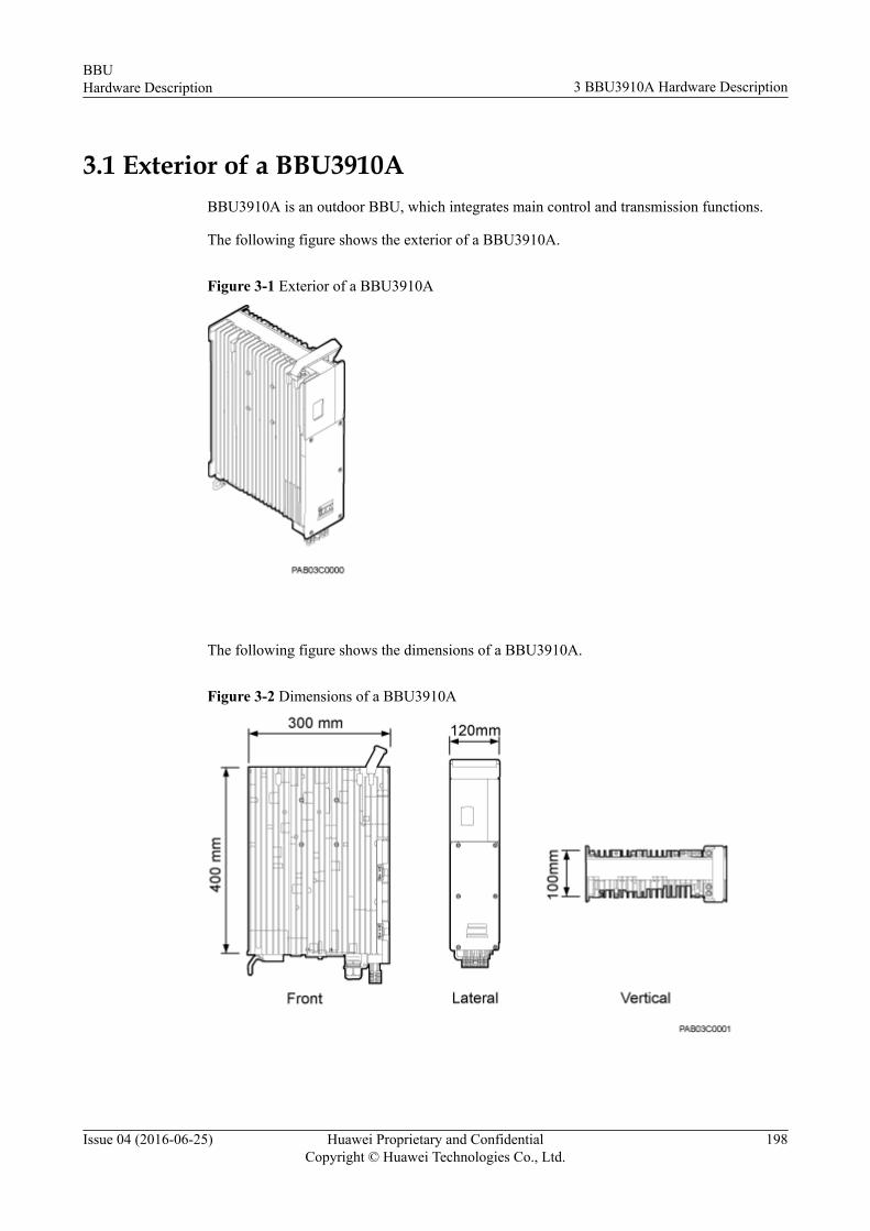
3.1 Exterior of a BBU3910ABBU3910A is an outdoor BBU, which integrates main control and transmission functions.
The following figure shows the exterior of a BBU3910A.
Figure 3-1 Exterior of a BBU3910A
The following figure shows the dimensions of a BBU3910A.
Figure 3-2 Dimensions of a BBU3910A
BBUHardware Description 3 BBU3910A Hardware Description
Issue 04 (2016-06-25) Huawei Proprietary and ConfidentialCopyright © Huawei Technologies Co., Ltd.
198
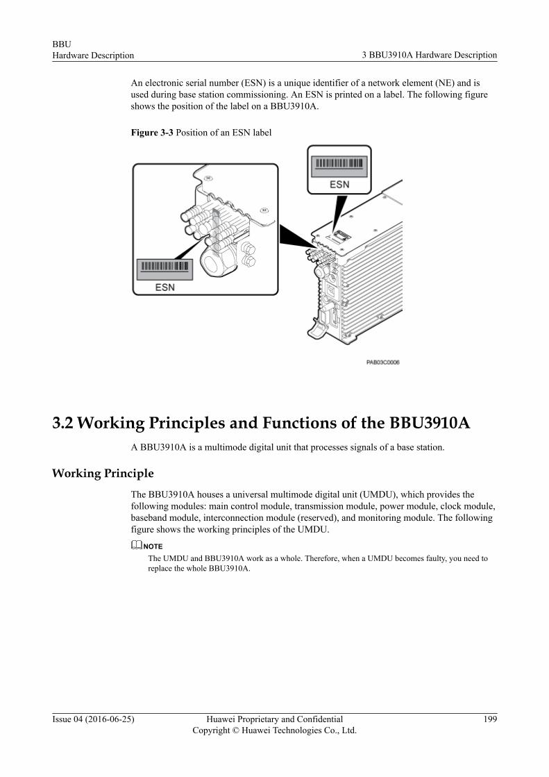
An electronic serial number (ESN) is a unique identifier of a network element (NE) and isused during base station commissioning. An ESN is printed on a label. The following figureshows the position of the label on a BBU3910A.
Figure 3-3 Position of an ESN label
3.2 Working Principles and Functions of the BBU3910AA BBU3910A is a multimode digital unit that processes signals of a base station.
Working PrincipleThe BBU3910A houses a universal multimode digital unit (UMDU), which provides thefollowing modules: main control module, transmission module, power module, clock module,baseband module, interconnection module (reserved), and monitoring module. The followingfigure shows the working principles of the UMDU.
NOTEThe UMDU and BBU3910A work as a whole. Therefore, when a UMDU becomes faulty, you need toreplace the whole BBU3910A.
BBUHardware Description 3 BBU3910A Hardware Description
Issue 04 (2016-06-25) Huawei Proprietary and ConfidentialCopyright © Huawei Technologies Co., Ltd.
199

Figure 3-4 Working principles of the UMDU in a BBU3910A
Function
The BBU3910A performs the following functions in a base station:
l Provides ports for connecting to the transmission equipment, RF modules, USB devicesa,external reference clock, and LMT or U2000 to transmit signals, perform automaticsoftware upgrade, receive reference clock signals, and support BBU maintenance on theLMT or U2000.
l Manages the entire base station system. The management involves the uplink anddownlink data processing, signaling processing, resource management, and operationand maintenance.
NOTE
a: The security of the USB port is ensured by encryption, and the USB port can be shut down usingcommands. The USB commissioning port is used for commissioning a base station rather thanconfiguring and exporting information of the base station.
3.3 BBU3910A Technical SpecificationsThis section describes the technical specifications of a BBU3910A, including capacityspecifications, signaling specifications, specifications of CPRI ports, transmission portspecifications, and engineering specifications.
BBUHardware Description 3 BBU3910A Hardware Description
Issue 04 (2016-06-25) Huawei Proprietary and ConfidentialCopyright © Huawei Technologies Co., Ltd.
200

Capacity Specifications
Table 3-1 provides the capacity specifications of a BBU3910A working in GSM mode.
Table 3-1 Capacity specifications of a BBU3910A working in GSM mode
Module Specifications
BBU3910A1 A single site supports a maximum of 12 cells and each cell supports amaximum of 24 TRXs.l IP over FE transmission: 72 TRXsl IP over E1 transmission: 48 TRXs
BBU3910A2
BBU3910A3
Table 3-2 provides the capacity specifications of a BBU3910A working in UMTS mode.
Table 3-2 Capacity specifications of a BBU3910A working in UMTS mode
Module
Numberof 2RCells
UplinkCE
Downlink CE
NumberofHSDPACodes
NumberofHSDPAUEs
NumberofHSUPAUEs
BBU3910A1
6 512 512 12 x 15 384 384
BBU3910A2
6 768 768 12x15 512 512
BBU3910A3
12 1024 1024 12 x 15 768 768
Table 3-3 provides the capacity specifications of a BBU3910A working in LTE FDD mode.
Table 3-3 Capacity specifications of a BBU3910A working in LTE FDD mode
Module MaximumNumber ofCells per BBU
MaximumThroughputper eNodeBFDD (PacketSize: 550Bytes)
MaximumNumber ofUEs in RRCConnectedMode pereNodeB FDD
MaximumNumber ofDRBs pereNodeB FDD
BBU3910A1
3 cells (2T2R/2T4R/4T4R, 20MHz)
Sum of uplinkand downlinkdata rates at theMAC layer: 825Mbit/s
l Datacardtraffic model:3600
l Smartphonetraffic model:1500
10800
BBUHardware Description 3 BBU3910A Hardware Description
Issue 04 (2016-06-25) Huawei Proprietary and ConfidentialCopyright © Huawei Technologies Co., Ltd.
201
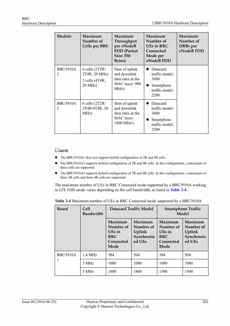
Module MaximumNumber ofCells per BBU
MaximumThroughputper eNodeBFDD (PacketSize: 550Bytes)
MaximumNumber ofUEs in RRCConnectedMode pereNodeB FDD
MaximumNumber ofDRBs pereNodeB FDD
BBU3910A2
6 cells (2T2R/2T4R, 20 MHz)3 cells (4T4R,20 MHz)
Sum of uplinkand downlinkdata rates at theMAC layer: 900Mbit/s
l Datacardtraffic model:3600
l Smartphonetraffic model:2200
BBU3910A3
6 cells (2T2R/2T4R/4T4R, 20MHz)
Sum of uplinkand downlinkdata rates at theMAC layer:1800 Mbit/s
l Datacardtraffic model:3600
l Smartphonetraffic model:2200
NOTE
l The BBU3910A1 does not support hybrid configuration of 2R and 4R cells.
l The BBU3910A2 supports hybrid configuration of 2R and 4R cells. In this configuration, a maximum ofthree cells are supported.
l The BBU3910A3 supports hybrid configuration of 2R and 4R cells. In this configuration, a maximum ofthree 2R cells and three 4R cells are supported.
The maximum number of UEs in RRC Connected mode supported by a BBU3910A workingin LTE FDD mode varies depending on the cell bandwidth, as listed in Table 3-4.
Table 3-4 Maximum number of UEs in RRC Connected mode supported by a BBU3910A
Board CellBandwidth
Datacard Traffic Model Smartphone TrafficModel
MaximumNumber ofUEs inRRCConnectedMode
MaximumNumber ofUplinkSynchronized UEs
MaximumNumber ofUEs inRRCConnectedMode
MaximumNumber ofUplinkSynchronized UEs
BBU3910A1
1.4 MHz 504 504 504 504
3 MHz 1080 1080 1080 1080
5 MHz 1800 1800 1500 1500
BBUHardware Description 3 BBU3910A Hardware Description
Issue 04 (2016-06-25) Huawei Proprietary and ConfidentialCopyright © Huawei Technologies Co., Ltd.
202

Board CellBandwidth
Datacard Traffic Model Smartphone TrafficModel
MaximumNumber ofUEs inRRCConnectedMode
MaximumNumber ofUplinkSynchronized UEs
MaximumNumber ofUEs inRRCConnectedMode
MaximumNumber ofUplinkSynchronized UEs
10 MHz, 15MHz, or 20MHz
3600 3600 1500 1500
BBU3910A2/BBU3910A3
1.4 MHz 1008 1008 1008 1008
3 MHz 2160 2160 2160 2160
5 MHz, 10MHz, 15MHz, or 20MHz
3600 3600 2200 2200
Table 3-5 lists the maximum number of UEs in RRC Connected mode per cell supported by aBBU3910A working in LTE FDD mode.
Table 3-5 Maximum number of UEs in RRC Connected mode per cell supported by aBBU3910A
Cell Bandwidth Maximum Number ofUEs in RRC ConnectedMode per Cell
Maximum Number ofUplink SynchronizedUEs per Cell
1.4 MHz 168 168
3 MHz 360 360
5 MHz 600 600
10 MHz, 15 MHz, or 20MHz
1200 1200
The maximum number of DRBs per UE supported by an eNodeB FDD is 8.
For the uplink and downlink throughput per UE and per cell supported by an eNodeB FDD,see Throughput in Technical Specifications of the eNodeB FDD.
Table 3-6 provides the capacity specifications of a BBU3910A working in LTE TDD mode.
BBUHardware Description 3 BBU3910A Hardware Description
Issue 04 (2016-06-25) Huawei Proprietary and ConfidentialCopyright © Huawei Technologies Co., Ltd.
203
Table 3-6 Capacity specifications of a BBU3910A working in LTE TDD mode
Module MaximumNumber ofCells per BBU
MaximumThroughputper eNodeBTDD (PacketSize: 550Bytes)
MaximumNumber ofUEs in RRCConnectedMode pereNodeB TDD
MaximumNumber ofDRBs pereNodeB TDD
BBU3910A1 3l 4T4R
beamforming: 10 MHz, 15MHz, or 20MHz cellbandwidth
l DL 2x2MIMO: 10MHz, 15MHz, or 20MHz cellbandwidth
l DL 4x4MIMO: 10MHz, 15MHz, or 20MHz cellbandwidth
Sum of uplinkand downlinkdata rates at theMAC layer: 825Mbit/s
l Datacardtrafficmodel: 3600
l Smartphonetrafficmodel: 1500
10800
BBU3910A3 6l 4T4R
beamforming: 10 MHz, 15MHz, or 20MHz cellbandwidth
l DL 2x2MIMO: 10MHz, 15MHz, or 20MHz cellbandwidth
l DL 4x4MIMO: 10MHz, 15MHz, or 20MHz cellbandwidth
Sum of uplinkand downlinkdata rates at theMAC layer:1800 Mbit/s
l Datacardtrafficmodel: 3600
l Smartphonetrafficmodel: 2200
The maximum number of UEs in RRC Connected mode supported by a BBU3910A workingin LTE TDD mode varies depending on the cell bandwidth, as listed in Table 3-7.
BBUHardware Description 3 BBU3910A Hardware Description
Issue 04 (2016-06-25) Huawei Proprietary and ConfidentialCopyright © Huawei Technologies Co., Ltd.
204
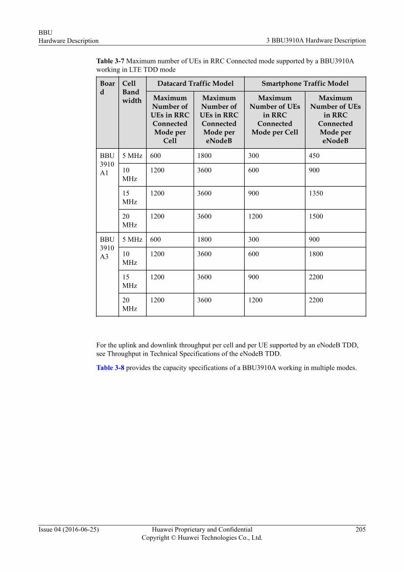
Table 3-7 Maximum number of UEs in RRC Connected mode supported by a BBU3910Aworking in LTE TDD mode
Board
CellBandwidth
Datacard Traffic Model Smartphone Traffic Model
MaximumNumber ofUEs in RRCConnectedMode per
Cell
MaximumNumber ofUEs in RRCConnectedMode pereNodeB
MaximumNumber of UEs
in RRCConnected
Mode per Cell
MaximumNumber of UEs
in RRCConnectedMode pereNodeB
BBU3910A1
5 MHz 600 1800 300 450
10MHz
1200 3600 600 900
15MHz
1200 3600 900 1350
20MHz
1200 3600 1200 1500
BBU3910A3
5 MHz 600 1800 300 900
10MHz
1200 3600 600 1800
15MHz
1200 3600 900 2200
20MHz
1200 3600 1200 2200
For the uplink and downlink throughput per cell and per UE supported by an eNodeB TDD,see Throughput in Technical Specifications of the eNodeB TDD.
Table 3-8 provides the capacity specifications of a BBU3910A working in multiple modes.
BBUHardware Description 3 BBU3910A Hardware Description
Issue 04 (2016-06-25) Huawei Proprietary and ConfidentialCopyright © Huawei Technologies Co., Ltd.
205

Table 3-8 Capacity specifications of a BBU3910A working in multiple modes
Module GU Scenario GL Scenario UL Scenario GUL Scenario
BBU3910A1
GSM G16/16/16+ UMTS 3x2UMTS: 512 CEsin the uplink and768 CEs in thedownlink
GSM G16/16/16+ LTE FDD3x20 MHzLTE FDD:4T4R; sum ofuplink anddownlink datarates at theMAC layer pereNodeB: 900Mbit/s
UMTS 3x2 +LTE FDD 3x20MHzl UMTS: 256
CEs in theuplink and384 CEs inthe downlink
l LTE FDD:2T2R; sumof uplink anddownlinkdata rates atthe MAClayer pereNodeB: 450Mbit/s
Not supported
BBU3910A2
GSM G16/16/16+ UMTS 3x2UMTS: 768 CEsin the uplink and768 CEs in thedownlink
GSM G16/16/16+ LTE FDD3x20 MHzLTE FDD:4T4R; sum ofuplink anddownlink datarates at theMAC layer pereNodeB: 900Mbit/s
UMTS 3x2 +LTE FDD 3x20MHzl UMTS: 384
CEs in theuplink and512 CEs inthe downlink
l LTE FDD:2T2R; sumof uplink anddownlinkdata rates atthe MAClayer pereNodeB: 450Mbit/s
Not supported
BBUHardware Description 3 BBU3910A Hardware Description
Issue 04 (2016-06-25) Huawei Proprietary and ConfidentialCopyright © Huawei Technologies Co., Ltd.
206
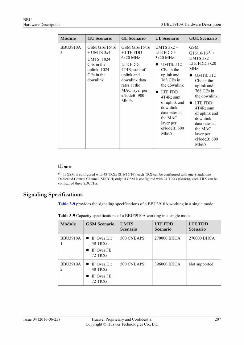
Module GU Scenario GL Scenario UL Scenario GUL Scenario
BBU3910A3
GSM G16/16/16+ UMTS 3x4UMTS: 1024CEs in theuplink, 1024CEs in thedownlink
GSM G16/16/16+ LTE FDD6x20 MHzLTE FDD:4T4R; sum ofuplink anddownlink datarates at theMAC layer pereNodeB: 900Mbit/s
UMTS 3x2 +LTE FDD 33x20 MHzl UMTS: 512
CEs in theuplink and768 CEs inthe downlink
l LTE FDD:4T4R; sumof uplink anddownlinkdata rates atthe MAClayer pereNodeB: 600Mbit/s
GSMG16/16/16(1) +UMTS 3x2 +LTE FDD 3x20MHzl UMTS: 512
CEs in theuplink and768 CEs inthe downlink
l LTE FDD:4T4R; sumof uplink anddownlinkdata rates atthe MAClayer pereNodeB: 600Mbit/s
NOTE
(1): If GSM is configured with 48 TRXs (S16/16/16), each TRX can be configured with one StandaloneDedicated Control Channel (SDCCH) only; if GSM is configured with 24 TRXs (S8/8/8), each TRX can beconfigured three SDCCHs.
Signaling SpecificationsTable 3-9 provides the signaling specifications of a BBU3910A working in a single mode.
Table 3-9 Capacity specifications of a BBU3910A working in a single mode
Module GSM Scenario UMTSScenario
LTE FDDScenario
LTE TDDScenario
BBU3910A1
l IP Over E1:48 TRXs
l IP Over FE:72 TRXs
500 CNBAPS 270000 BHCA 270000 BHCA
BBU3910A2
l IP Over E1:48 TRXs
l IP Over FE:72 TRXs
500 CNBAPS 396000 BHCA Not supported
BBUHardware Description 3 BBU3910A Hardware Description
Issue 04 (2016-06-25) Huawei Proprietary and ConfidentialCopyright © Huawei Technologies Co., Ltd.
207

Module GSM Scenario UMTSScenario
LTE FDDScenario
LTE TDDScenario
BBU3910A3
l IP Over E1:48 TRXs
l IP Over FE:72 TRXs
600 CNBAPS 396000 BHCA 396000 BHCA
Table 3-10 provides the signaling specifications of a BBU3910A working in multiple modes.
Table 3-10 Signaling specifications of a BBU3910A working in multiple modes
Module GU Scenario GL Scenario UL Scenario GUL Scenario
BBU3910A1
GSM 48 TRX +UMTS 200CNBAPS
GSM 48 TRX +LTE 110000BHCA
UMTS 200CNBAPS + LTE110000 BHCA
Not supported
BBU3910A2
GSM 48 TRX +UMTS 200CNBAPS
GSM 48 TRX +LTE 220000BHCA
UMTS 200CNBAPS + LTE110000 BHCA
Not supported
BBU3910A3
GSM 48 TRX +UMTS 300CNBAPS
GSM 48 TRX +LTE 220000BHCA
UMTS 300CNBAPS + LTE110000 BHCA
GSM 36 TRX +UMTS 300CNBAPS + LTE110000 BHCA
Specifications of CPRI PortsTable 3-11 provides specifications of CPRI ports on a BBU3910A.
Table 3-11 Specifications of CPRI ports on a BBU3910A
Module Quantity of CPRIPorts
CPRI Data Rate(Gbit/s)
Topology
BBU3910A1/BBU3910A2/BBU3910A3
6 1.25/2.5/4.9/6.144/9.8
Star, chain, or ring
CPRI ports with different data rates support different numbers of TRXs or cells, as listed inTable 3-12.
BBUHardware Description 3 BBU3910A Hardware Description
Issue 04 (2016-06-25) Huawei Proprietary and ConfidentialCopyright © Huawei Technologies Co., Ltd.
208

Table 3-12 Mapping between the CPRI port rate and the number of TRXs/cells (GSM,UMTS, LTE FDD)
CPRIDataRate(Gbit/s)
GSM UMTS LTE FDD
Number of1T2RTRXs
Number of2T2R or1T4RTRXs
Number of1T2RCells
Numberof 2T2RCells
Number of2T4R or4T4R Cells
Number of1T2R or2T2R Cells
1.25 24 12 4 4(2) 4x4 MIMOcells are notrecommendedbecause thetransmissionbandwidth ofthe CPRI portsis limited.
l 4 (cellbandwidth≤ 3 MHz)
l 2 (cellbandwidth≤ 5 MHz)
l 1 (cellbandwidth≤ 10 MHz)
2.5 48 24 8 8(2) 1 (cellbandwidth ≤10 MHz)
l 4 (cellbandwidth≤ 5 MHz)
l 2 (cellbandwidth≤ 10 MHz)
l 1 (cellbandwidth= 15 MHzor 20MHz)
4.9 48 24 16 16(2) l 2 (cellbandwidth≤ 10 MHz)
l 1 (cellbandwidth= 15 MHzor 20MHz)
l 4 (cellbandwidth≤ 10 MHz)
l 2 (cellbandwidth= 15 MHzor 20MHz)
6.144 — — 24 24(2) l 2 (cellbandwidth≤ 10 MHz)
l 1 (cellbandwidth= 15 MHzor 20MHz)
l 4 (cellbandwidth≤ 10 MHz)
l 2 (cellbandwidth= 15 MHzor 20MHz)
BBUHardware Description 3 BBU3910A Hardware Description
Issue 04 (2016-06-25) Huawei Proprietary and ConfidentialCopyright © Huawei Technologies Co., Ltd.
209

CPRIDataRate(Gbit/s)
GSM UMTS LTE FDD
Number of1T2RTRXs
Number of2T2R or1T4RTRXs
Number of1T2RCells
Numberof 2T2RCells
Number of2T4R or4T4R Cells
Number of1T2R or2T2R Cells
9.8 48 24 32 32(2) l 4 (cellbandwidth≤ 10 MHz)
l 2 (cellbandwidth= 15 MHzor 20MHz)
l 8 (cellbandwidth≤ 10 MHz)
l 4 (cellbandwidth= 15 MHzor 20MHz)
NOTE
(2): The number of 2T2R cells is halved if two TX antennas enabled with the virtual antenna mapping (VAM)function are separately connected to two RF modules carried on different CPRI links.
CPRI ports with different data rates support different numbers of LTE TDD cells, as listed inTable 3-13.
Table 3-13 Mapping between the CPRI port rate and the number of cells (LTE TDD)
CPRI Data Rate(Gbit/s)
CPRICompression(3)
Number of 4T4RCells
Number of 2T2RCells
2.5 Not in use l 2 (cell bandwidth = 5MHz)
l 1 (cell bandwidth =10 MHz)
l None (cell bandwidth= 15 MHz or 20MHz)
l 4 (cell bandwidth = 5MHz)
l 2 (cell bandwidth =10 MHz)
l 1 (cell bandwidth =15 MHz or 20 MHz)
In use l None (cell bandwidth= 5 MHz)
l 1 (cell bandwidth =10 MHz)
l 1 (cell bandwidth =15 MHz)
l 1 (cell bandwidth =20 MHz)
l None (cell bandwidth= 5 MHz)
l 3 (cell bandwidth =10 MHz)
l 2 (cell bandwidth =15 MHz)
l 2 (cell bandwidth =20 MHz)
BBUHardware Description 3 BBU3910A Hardware Description
Issue 04 (2016-06-25) Huawei Proprietary and ConfidentialCopyright © Huawei Technologies Co., Ltd.
210

CPRI Data Rate(Gbit/s)
CPRICompression(3)
Number of 4T4RCells
Number of 2T2RCells
4.9 Not in use l 4 (cell bandwidth = 5MHz)
l 2 (cell bandwidth =10 MHz)
l 1 (cell bandwidth =15 MHz or 20 MHz)
l 8 (cell bandwidth = 5MHz)
l 4 (cell bandwidth =10 MHz)
l 2 (cell bandwidth =15 MHz or 20 MHz)
In use l None (cell bandwidth= 5 MHz)
l 3 (cell bandwidth =10 MHz)
l 2 (cell bandwidth =15 MHz)
l 2 (cell bandwidth =20 MHz)
l None (cell bandwidth= 5 MHz)
l 6 (cell bandwidth =10 MHz)
l 4 (cell bandwidth =15 MHz)
l 4 (cell bandwidth =20 MHz)
9.8 Not in use l 8 (cell bandwidth = 5MHz)
l 4 (cell bandwidth =10 MHz)
l 2 (cell bandwidth =15 MHz or 20 MHz)
l 16 (cell bandwidth =5 MHz)
l 8 (cell bandwidth =10 MHz)
l 4 (cell bandwidth =15 MHz or 20 MHz)
In use l None (cell bandwidth= 5 MHz or 15 MHz)
l 6 (cell bandwidth =10 MHz)
l 4 (cell bandwidth =15 MHz)
l 4 (cell bandwidth =20 MHz)
l None (cell bandwidth= 5 MHz)
l 12 (cell bandwidth =10 MHz)
l 8 (cell bandwidth =15 MHz)
l 8 (cell bandwidth =20 MHz)
NOTE
(3): CPRI compression is not supported when the cell bandwidth is 5 MHz.
Transmission PortTable 3-14 provides specifications of transmission ports on a BBU3910A.
BBUHardware Description 3 BBU3910A Hardware Description
Issue 04 (2016-06-25) Huawei Proprietary and ConfidentialCopyright © Huawei Technologies Co., Ltd.
211

Table 3-14 Transmission port
Module Transmission Port Type Quantity of Ports
BBU3910A1/BBU3910A2/BBU3910A3
E1/T1 port 4 (4 E1s/T1s)
FE/GE electrical port 1
FE/GE optical port 1
Equipment Specifications
Table 3-15 lists the input power specifications of a BBU3910A.
Table 3-15 Input power specifications
Module Input Power Voltage Range
BBU3910A1/BBU3910A2/BBU3910A3
-48 V DC -38.4 V DC to -57 V DC
Table 3-16 lists the dimensions and weight of a BBU3910A.
Table 3-16 Dimensions and weight of a BBU3910A
Module Dimensions (HxWxD) Weight
BBU3910A1/BBU3910A2/BBU3910A3
400 mm x 300 mm x 100mm
≤ 12 kg
Table 3-17 provides the heat dissipation capabilities of a BBU3910A.
Table 3-17 Heat dissipation capabilities of a BBU3910A
Module Specifications
BBU3910A1/BBU3910A2/BBU3910A3 150 W
Table 3-18 lists the environmental specifications of a BBU3910A.
Table 3-18 Environmental specifications
Item Specifications
Operating temperature Without solar radiation: -40°C to +55°C
Relative humidity 5% RH to 100% RH
BBUHardware Description 3 BBU3910A Hardware Description
Issue 04 (2016-06-25) Huawei Proprietary and ConfidentialCopyright © Huawei Technologies Co., Ltd.
212
Item Specifications
Atmospheric pressure 60 kPa to 106 kPa
Table 3-19 lists the surge protection specifications for ports on a BBU3910A.
NOTE
l Unless otherwise specified, the surge protection specifications depend on the surge waveform of 8/20 μs.
l All the surge current items, unless otherwise specified as Maximum discharge current, refer toNominal discharge current.
Table 3-19 Surge protection specifications for ports on a BBU3910A
Port Surge Protection Mode Surge ProtectionSpecifications
-48 V DC port Surge current 20 kA
Table 3-20 lists the compliance standards for a BBU3910A.
Table 3-20 Compliance standards for a BBU3910A
Item Standard
Securitystandards
l IEC 60950-1:2005 (2nd Edition) + A1:2009 + National & GroupDifferences per CB Bulletin Information technology equipment -SafetyPart1:General requirements
l IEC 60950-22:2005 (1st Edition) + National & Group Differences per CBBulletin Information technology equipment - Safety - Part 22:Equipmentinstalled outdoors
l IEC 60215(1987)+A1:1990+A2:1993 + National & Group Differences perCB Bulletin Safety requirement for radio transmitting equipment
IngressProtection(IP) rating
IP65
Operatingenvironment
ETS 300 019-1-4 Class 4.1
Storageenvironment
ETSI EN300019-1-1 V2.1.4 (2003-04) class1.2 "Weatherprotected, nottemperature-controlled storage locations"NOTE
l The validity period is one year.
l The product can function properly within the validity period if the storageenvironment meets the preceding standards.
BBUHardware Description 3 BBU3910A Hardware Description
Issue 04 (2016-06-25) Huawei Proprietary and ConfidentialCopyright © Huawei Technologies Co., Ltd.
213
Item Standard
Transportationenvironment
EUROPEAN ETS 300 019-1-2 Class 2.3 "PUBLIC transportation"
Anti-earthquakeperformance
l IEC 60068-2-57:Environmental testing -Part 2-57:Tests -Test Ff:Vibration-Time-history method
l ETSI EN 300019-1-4: "Earthquake"l YD5083:Interim Provisions for Test of Anti-seismic Performances of
Telecommunications Equipment (telecom industry standard in People'sRepublic of China)
l NEBS GR63 zone4
Protectionstandards
l GB50689-2011, YD2324-2011l ITU-T K.21/44
EMC l R&TTE Directive 1999/5/ECl EN 55022 CLASS Bl ETSI EN 301 489-01l ETSI EN 301 489-23(WCDMA/LTE)l FCC part 15 CLASS B
Surgeprotection
l IEC 62305-1 Protection against lightning - Part 1:General principlesl IEC 62305-3 Protection against lightning - Part 3:Physical damage to
structures and life hazardl IEC 62305-4 Protection against lightning - Part 4:Electrical and electronic
systems within structuresl ITU-T K.35 Bonding configurations and earthing at remote electronic sitesl ITU-T K.56 Protection of radio base stations against lightning dischargesl ITU-T K.97 Lightning protection of distributed base stationsl ETSI EN 300 253 Environmental Engineering(EE):Earthing and bonding
configuration inside telecommunications centersl YD 2324-2011 Lightning protection requirements and test methods for
Radio Base Stations (RBSs)l GB/T 50689-2011 Code for design of lightning protection and earthing
engineering for telecommunication bureaus (stations)
3.4 Ports on a BBU3910AThis section describes ports on BBU3910A panels, including a bottom panel, a cabling cavitypanel, and an indicator panel.
The following figure shows the ports on BBU3910A panels.
BBUHardware Description 3 BBU3910A Hardware Description
Issue 04 (2016-06-25) Huawei Proprietary and ConfidentialCopyright © Huawei Technologies Co., Ltd.
214
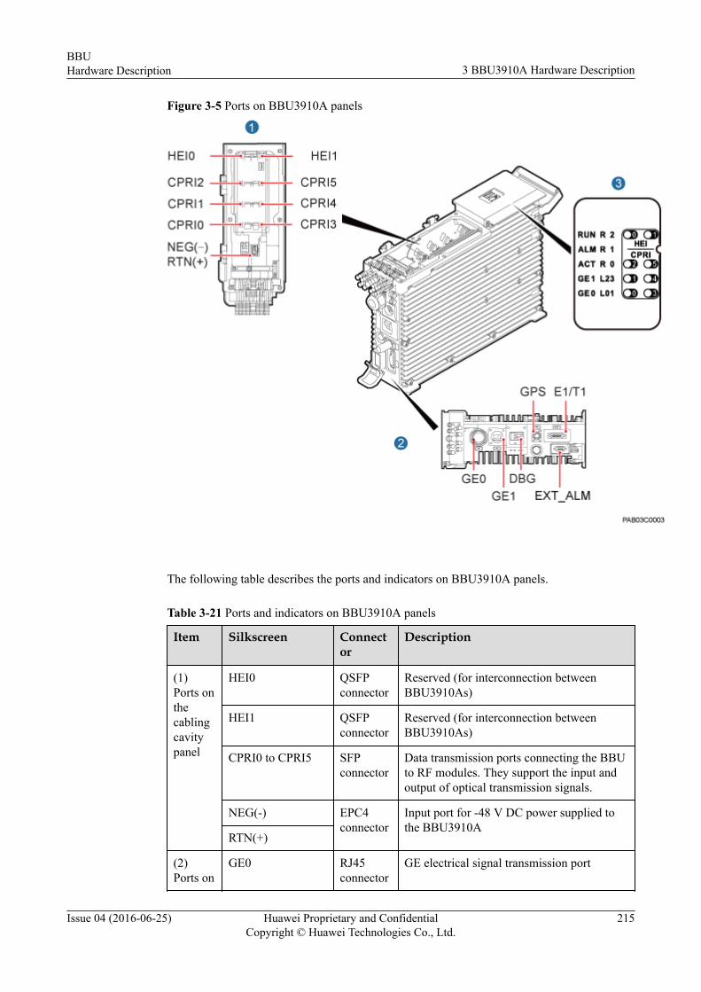
Figure 3-5 Ports on BBU3910A panels
The following table describes the ports and indicators on BBU3910A panels.
Table 3-21 Ports and indicators on BBU3910A panels
Item Silkscreen Connector
Description
(1)Ports onthecablingcavitypanel
HEI0 QSFPconnector
Reserved (for interconnection betweenBBU3910As)
HEI1 QSFPconnector
Reserved (for interconnection betweenBBU3910As)
CPRI0 to CPRI5 SFPconnector
Data transmission ports connecting the BBUto RF modules. They support the input andoutput of optical transmission signals.
NEG(-) EPC4connector
Input port for -48 V DC power supplied tothe BBU3910A
RTN(+)
(2)Ports on
GE0 RJ45connector
GE electrical signal transmission port
BBUHardware Description 3 BBU3910A Hardware Description
Issue 04 (2016-06-25) Huawei Proprietary and ConfidentialCopyright © Huawei Technologies Co., Ltd.
215
Item Silkscreen Connector
Description
thebottompanel
GE1 SFPconnector
GE optical signal transmission port
DBG USBconnector
l Used for the software upgrade of a basestation using a USB flash drive.
l Used as a local maintenance port whenconnecting to a WLAN adapter.
l Port for clock signal outputs. The clocksignals are used for testing.
RJ45connector
Commissioning port, which is connected tothe LMT for commissioning a base station
EXT_ALM DB15femaleconnector
Port for monitoring environmental alarms,which transmits one channel of RS485signals or six channels of dry contact inputsand one channel of dry contact output
E1/T1 DB26femaleconnector
E1/T1 signal transmission port
GPS Type Nfemaleconnector
GPS port for forwarding RF signals from theantenna to the satellite card
(3)Indicators
l RUNl ALMl ACTl GE0, GE1l R0, R1, R2l L01, L23l HEI0, HEI1l CPRI0, CPRI1,
CPRI2, CPRI3,CPRI4, andCPRI5
- For details, see 3.5 Indicators on aBBU3910A.
3.5 Indicators on a BBU3910AThere are 18 indicators on a BBU3910A. They indicate the running status of the BBU3910A.
For the positions of indicators on a BBU3910A, see 3.4 Ports on a BBU3910A.
The following table describes the indicators on a BBU3910A.
BBUHardware Description 3 BBU3910A Hardware Description
Issue 04 (2016-06-25) Huawei Proprietary and ConfidentialCopyright © Huawei Technologies Co., Ltd.
216
Table 3-22 Indicators on a BBU3910A
Silkscreen
Color Status Description
RUN Green Steady on There is power supply.
Steady off l There is no power supply.l The board is faulty.
Blinking (onfor 1s and offfor 1s)
The board is running properly.
Blinking (onfor 0.125s andoff for 0.125s)
l The board is being loaded or configured.l The board is not started.
ALM Red Steady on An alarm is generated, and the board needs to bereplaced.
Steady off The board is running properly.
Blinking (onfor 1s and offfor 1s)
An alarm is generated, and you need to locatethe fault before determining whether to replacethe board.
ACT Green Steady on l The board is serving as an active board.l The board has been activated and is
providing services.
Steady off l The board is not serving as an active board.l The board has not been activated or is not
providing any services.
Blinking (onfor 0.125s andoff for 0.125s)
The operation and maintenance link (OML) isdisconnected.
Blinking (onfor 1s and offfor 1s)
The board is being tested, for example, goingthrough an RRU voltage standing wave ratio(VSWR) test by using a USB flash drive.NOTE
Only the BBU3910A working in UMTS mode has thisindicator status.
Blinking (Inevery 4s, theindicator is onfor 0.125s andoff for 0.125s[eight times] inthe first 2s andthen off for 2s.)
l All cells configured for the subrack thathouses this board are not activated.
l The S1 link is faulty.NOTE
Only the BBU3910A working in LTE mode has thisindicator status.
GE0 Green Steady on The Ethernet link is functioning properly.
BBUHardware Description 3 BBU3910A Hardware Description
Issue 04 (2016-06-25) Huawei Proprietary and ConfidentialCopyright © Huawei Technologies Co., Ltd.
217

Silkscreen
Color Status Description
Steady off The network cable is not connected.
GE1 Red orgreen
Steady green The Ethernet link is functioning properly.
Steady red The optical module is transmitting or receivingfaulty.
Blinking red(on for 1s andoff for 1s)
Ethernet negotiation is faulty.
Steady off The SFP module cannot be detected, or theoptical module is powered off.
R0 Red orgreen
Steady off The board is not working in GSM mode.
Steady green The board is working in GSM mode.
R1 Red orgreen
Steady off The board is not working in UMTS mode.
Steady green The board is working in UMTS mode.
R2 Red orgreen
Steady off The board is not working in LTE mode.
Steady green The board is working in LTE mode.
L01 Red orgreen
Steady off Links 0 and 1 are not set up, or LOS alarms aregenerated on the links.
Steady green Links 0 and 1 are functioning properly.
Blinking green(on for 1s andoff for 1s)
Link 0 is functioning properly, but link 1 is notset up or an LOS alarm is generated on link 1.
Blinking green(on for 0.125sand off for0.125s)
Link 1 is functioning properly, but link 0 is notset up or an LOS alarm is generated on link 0.
Steady red Alarms are generated on links 0 and 1.
Blinking red(on for 1s andoff for 1s)
An alarm is generated on link 0.
Blinking red(on for 0.125sand off for0.125s)
An alarm is generated on link 1.
L23 Red orgreen
Steady off Links 2 and 3 are not set up, or LOS alarms aregenerated on the links.
Steady green Links 2 and 3 are functioning properly.
BBUHardware Description 3 BBU3910A Hardware Description
Issue 04 (2016-06-25) Huawei Proprietary and ConfidentialCopyright © Huawei Technologies Co., Ltd.
218

Silkscreen
Color Status Description
Blinking green(on for 1s andoff for 1s)
Link 2 is functioning properly, but link 3 is notset up or an LOS alarm is generated on link 3.
Blinking green(on for 0.125sand off for0.125s)
Link 3 is functioning properly, but link 2 is notset up or an LOS alarm is generated on link 2.
Steady red Alarms are generated on links 2 and 3.
Blinking red(on for 1s andoff for 1s)
An alarm is generated on link 2.
Blinking red(on for 0.125sand off for0.125s)
An alarm is generated on link 3.
HEI0 Red orgreen
- Reserved
HEI1
CPRI0toCPRI5
Red orgreen
Steady green The CPRI link is functioning properly.
Steady red An optical module fails to transmit or receivesignals due to one of the following causes:l The optical module is faulty.l The fiber optic cable is broken.
Blinking red(on for 0.125sand off for0.125s)
The RF module connected to the CPRI port hasa hardware fault.
Blinking red(on for 1s andoff for 1s)
The CPRI link is out of lock due to one of thefollowing causes:l There is no mutual lock between dual-mode
reference clocks.l The CPRI port rate does not match the rate of
the optical module.l VSWR alarms are reported on the RF
module connected to the CPRI port when aVSWR test is conducted using a USB flashdrivea.
Steady off l The optical module cannot be detected.l The CPRI electrical cable is not connected.
BBUHardware Description 3 BBU3910A Hardware Description
Issue 04 (2016-06-25) Huawei Proprietary and ConfidentialCopyright © Huawei Technologies Co., Ltd.
219

Silkscreen
Color Status Description
a: The security of the USB port is ensured by encryption, and the USB port can be shutdown using commands.
BBUHardware Description 3 BBU3910A Hardware Description
Issue 04 (2016-06-25) Huawei Proprietary and ConfidentialCopyright © Huawei Technologies Co., Ltd.
220


