www.iunet.eu 1
Italian Universities NanoElectronics
Team
ConsorzioNazionale
Interuniversitarioper la
Nanoelettronica
www.iunet.eu 2
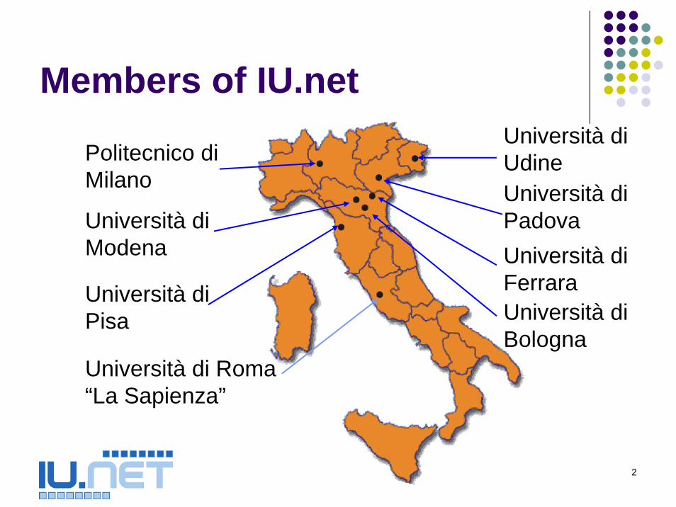
Members of IU.net
Politecnico di Milano
Università di UdineUniversità di PadovaUniversità di
Modena
Università di Pisa
Università di Ferrara
Università di Roma “La Sapienza”
Università di Bologna
www.iunet.eu 3
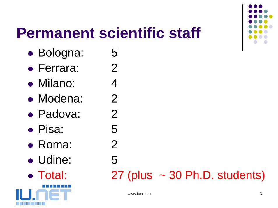
Permanent scientific staffBologna: 5Ferrara: 2Milano: 4Modena: 2Padova: 2Pisa: 5Roma: 2Udine: 5Total: 27 (plus ~ 30 Ph.D. students)

www.iunet.eu 4
Mission of the ConsortiumDevelop collaborative research between associate Universities and other public and private Research centersFoster collaboration with industry to jointly develop new ideas and concepts, and prove them at demonstrator levelPerform studies and research commissioned by private or public entities, by exploiting the means and the know-how of the associate members of IU.netDisseminate and valorize the Consortium know-how and competences by promoting the participation of associate members to national and international research projects

www.iunet.eu 5
Governance• Cor Claeys
IMEC, Leuven, Belgio
• Andrea LacaitaPolitecnico di Milano
• Alessandro PaccagnellaUniversità di Padova
• Luca SelmiUniversità di Udine
• Università di Bologna –Massimo Rudan
• Università di Ferrara –Piero Olivo
• Politecnico di Milano –Alessandro Spinelli
• Università di Modena –Paolo Pavan (Chairman)
• Università di Padova –Andrea Cester
• Università di Pisa –Giuseppe Iannaccone
• Università di Roma LS –Fernanda Irrera
• Università di Udine –David Esseni
Scientific Committee
Enrico Sangiorgi
Director
Assembly
location: via Toffano 2, Bologna

www.iunet.eu 6
Main research lines
Nano-transistors: CMOS and post-CMOSNanoelectronic non-volatile Memories
Providing support to the development of technology platforms for micro- and nano-electronics
www.iunet.eu 7
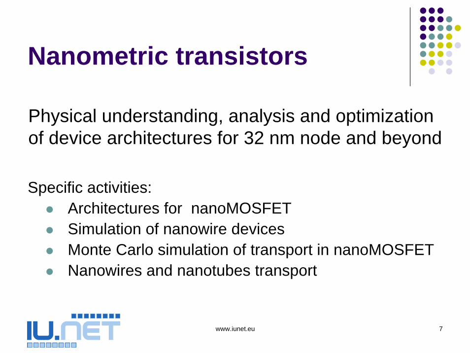
Nanometric transistors
Specific activities:Architectures for nanoMOSFETSimulation of nanowire devicesMonte Carlo simulation of transport in nanoMOSFETNanowires and nanotubes transport
Physical understanding, analysis and optimization of device architectures for 32 nm node and beyond

www.iunet.eu 8
Quasi-ballistic transport in nanoMOSFET
Lucci et al., IEDM 2005
www.iunet.eu 9
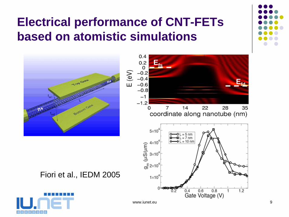
Electrical performance of CNT-FETsbased on atomistic simulations
Fiori et al., IEDM 2005
Efs
Efd

www.iunet.eu 10
Nanoelectronic NV Memories
Specific activities:Flash memoriesPhase-change memoriesNROM and SONOS MemoriesCharacterization and reliability assessmentRadiation effects on NVM performancesTechnology optimization
Assessment of innovative technologies for non-volatile nanoelectronic memories

www.iunet.eu 11
Phase-change memories
2001 2003 2005 2007 2009 2011 201310-3
10-2
10-1
100
32 nm
32 nm
180 nm
180 nm
130 nm
90 nm65 nm
45 nm
130 nm
90 nm
65 nm
45 nm
45 nm
65 nm
90 nm
demonstrator FLASH NOR FLASH NAND PCM
Cel
l siz
e (μ
m2 )
Year
I
V
Lacaita, EPCOS 2005

www.iunet.eu 12
SONOS and NROM memories
Drain Source
NO
Ohe
Gate
Channel
+-
ONO2F
Planar NROM
Larcher et al., TED 2004Arreghini et al.,INFOS 2005

www.iunet.eu 13
Ongoing projects
EC Project PULLNANOEC Project EMMANational Project PNR

www.iunet.eu 14
PULLing the limits of NANOcmos electronicsEC Contract N. 26828Period: 06/2006 - 05/2009Four companies (ST, Freescale, Philips, Infineon, ), four research institution (IMEC, CEA, Fraunhofer, CNRS), seventeen universities/consortia, three SMEsUniBO, UniUD, UniPI and PoliMI participating for IUNET (approx €660 000)Purpose: pulling forward CMOS Technologies: exploratory research; characterization; modelling and advance simulation; demonstration of feasibility of concepts; process modules integration; definition of specifications of advanced new equipment; demonstration of feasibility of a 32nm CMOS logic technology; exploratory action towards the 22nm node
EC Project PULLNANO
www.iunet.eu 15
IU.NET in PULLNANO
Role of IU.NETcoordination of WP/Cluster 6.4 «Advanced modelling and simulation»
Partners of the Cluster:IU.NETETHZTechnical University of WarsawCNRS
www.iunet.eu 16
PULLNANO WP6.4 Objectives
Develop advanced physical models addressing the needs foreseen for the 22nm technology node:
strained siliconadoption of different crystal orientations for the channelhigh-k gate dielectricsfluctuations of dopants, dielectric and silicon layer thickness and effects of line-edge roughness
Implement the developed models in device simulators and compare different device architectures and technological options

www.iunet.eu 17
EC Project EMMAEmerging Materials for Mass-storage ApplicationsPeriod: 09/2006 – 08/2009Two companies (ST, IMEC), two research institution (CNR-MDM, CNRS-L2MP) and two universities/consortia (RWTH Aachen, IUNET)PoliMI, UniPD and UniMORE participating for IUNETPurpose: demonstrating the feasibility of non volatile memories based on resistive switching for mass storage
www.iunet.eu 18
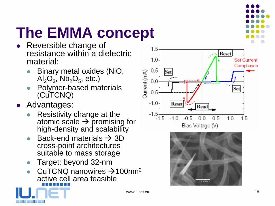
The EMMA conceptReversible change of resistance within a dielectric material:
Binary metal oxides (NiO, Al2O3, Nb2O5, etc.)Polymer-based materials (CuTCNQ)
Advantages:Resistivity change at the atomic scale promising for high-density and scalabilityBack-end materials 3D cross-point architectures suitable to mass storageTarget: beyond 32-nmCuTCNQ nanowires 100nm2
active cell area feasible
www.iunet.eu 19
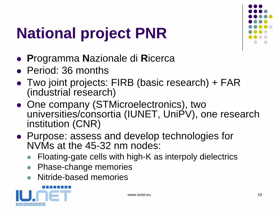
National project PNRProgramma Nazionale di RicercaPeriod: 36 monthsTwo joint projects: FIRB (basic research) + FAR (industrial research)One company (STMicroelectronics), twouniversities/consortia (IUNET, UniPV), one researchinstitution (CNR)Purpose: assess and develop technologies forNVMs at the 45-32 nm nodes:
Floating-gate cells with high-K as interpoly dielectricsPhase-change memoriesNitride-based memories
www.iunet.eu 20
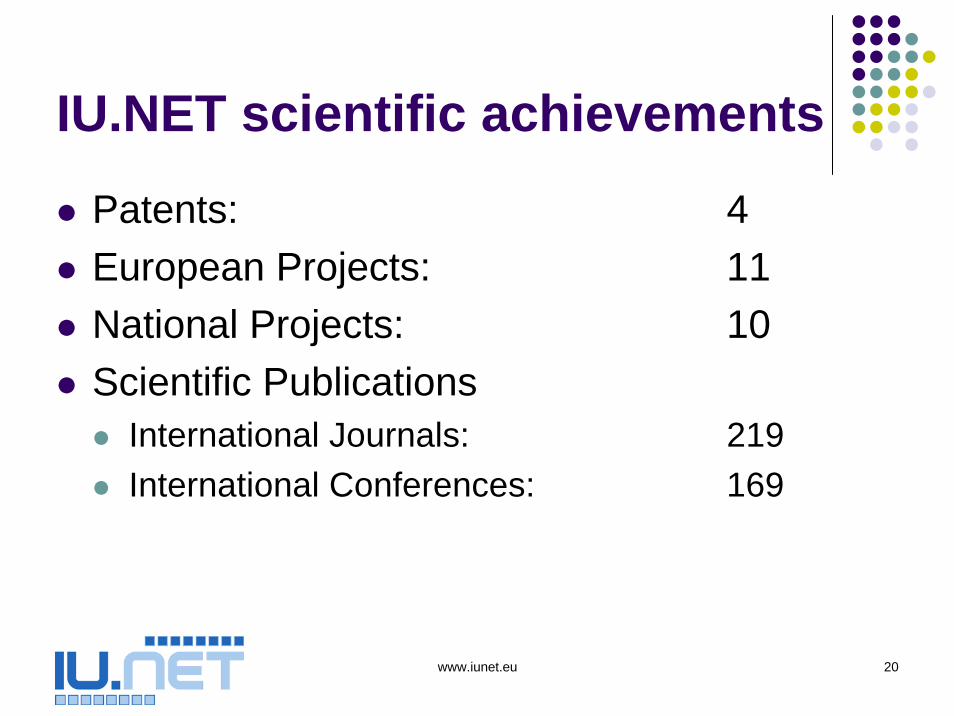
IU.NET scientific achievements
Patents: 4European Projects: 11National Projects: 10Scientific Publications
International Journals: 219International Conferences: 169
www.iunet.eu 21
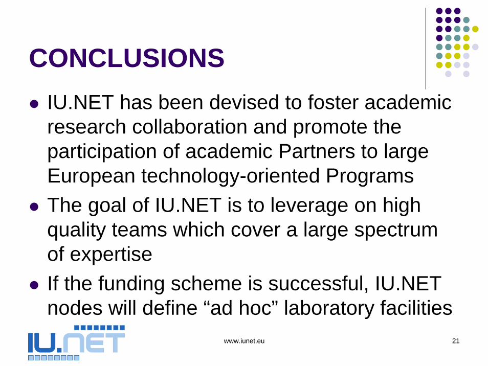
CONCLUSIONSIU.NET has been devised to foster academic research collaboration and promote the participation of academic Partners to large European technology-oriented ProgramsThe goal of IU.NET is to leverage on high quality teams which cover a large spectrum of expertiseIf the funding scheme is successful, IU.NET nodes will define “ad hoc” laboratory facilities


