
FPGA-BASED DIGITAL PHASE-LOCKED LOOP ANALYSIS AND
IMPLEMENTATION
BY
DAN HU
THESIS
Submitted in partial fulfillment of the requirements
for the degree of Master of Science in Electrical and Computer Engineering
in the Graduate College of the
University of Illinois at Urbana-Champaign, 2011
Urbana, Illinois
Advisers:
Professor Steven J. Franke
Visiting Lecturer Christopher D. Schmitz

Abstract
The thesis presents a digital PLL project that will be used as an ECE
463 lab module and serve as a platform for future communication research
projects. Field Programmable Gate Array (FPGA) technology is used for all
digital signal processing tasks. A Direct Digital Synthesizer (DDS) is used
to synthesize analog output, the frequency of which is controlled digitally by
the FPGA. This system is implemented in a way that makes it educational
and suitable for a lab module. Unlike purely digital PLL, this project in-
volves several analog circuits soldered on PCBs, which will help the students
visualize the signal flow in the PLL and get some exposure to mixed-signal
systems.
ii

Contents
1 Introduction . . . . . . . . . . . . . . . . . . . . . . . . . . . 1
2 Theory . . . . . . . . . . . . . . . . . . . . . . . . . . . . . . 32.1 PLL theory . . . . . . . . . . . . . . . . . . . . . . . . . . . . 32.2 Phase detector . . . . . . . . . . . . . . . . . . . . . . . . . . 72.3 DDS theory . . . . . . . . . . . . . . . . . . . . . . . . . . . . 112.4 Figures . . . . . . . . . . . . . . . . . . . . . . . . . . . . . . . 14
3 Implementation and Analysis . . . . . . . . . . . . . . . . 183.1 FPGA . . . . . . . . . . . . . . . . . . . . . . . . . . . . . . . 183.2 Other hardware . . . . . . . . . . . . . . . . . . . . . . . . . . 243.3 Modeling of actual system . . . . . . . . . . . . . . . . . . . . 243.4 Figures . . . . . . . . . . . . . . . . . . . . . . . . . . . . . . . 27
4 Experiment and Characterization . . . . . . . . . . . . . . 344.1 Constant parameters in experiment setup . . . . . . . . . . . . 344.2 Response to step stimulus . . . . . . . . . . . . . . . . . . . . 354.3 Response to sinusoidal stimulus . . . . . . . . . . . . . . . . . 374.4 Processing lag . . . . . . . . . . . . . . . . . . . . . . . . . . . 394.5 Lock range . . . . . . . . . . . . . . . . . . . . . . . . . . . . . 404.6 Figures . . . . . . . . . . . . . . . . . . . . . . . . . . . . . . . 42
5 Conclusion . . . . . . . . . . . . . . . . . . . . . . . . . . . . 47
References . . . . . . . . . . . . . . . . . . . . . . . . . . . . . . 48
iii

1 Introduction
Phase-locked loop (PLL) is a linear feedback control system that can gener-
ate an output signal which has the same frequency and, perhaps, phase as
the input reference signal. It consists of three major components: a phase
detector (PD) that computes the phase error of the output with respect to
the input reference signal, a loop filter that converts the phase error to a con-
trol voltage for the Voltage-Controlled Oscillator (VCO), and a VCO that
generates a sinusoidal output. PLL has been widely used in many radio com-
munication applications. For example, it can be used in a coherent receiver
to recover the carrier frequency that is modulated by the transmitted data.
In this thesis, we address issues that are related to FPGA implementation
of digital PLL and present experimental characterization results of our PLL
project.
Chapter 2 focuses on the theoretical concepts that are needed to under-
stand this PLL project. Section 2.1 summarizes the basic principles and
important characteristics of a generic digital PLL. Section 2.2 presents two
algorithms for phase detector implementation that are used in this project
and examines their limitations. Section 2.3 covers the theory of operation of
DDS, which is used as the digital VCO in our project.
Chapter 3 covers the implementation details of the project, with emphases
on FPGA programming and actual system modeling. Other hardware com-
ponents in this project, such as linear regulators and a ceramic filter, are also
1

introduced in this chapter.
Finally, we characterize various aspects of the real system with several
experiments. Chapter 4 explains the experiment setup and presents the mea-
surement results that are used to verify the validity of the analytical model
developed in Chapter 3.
2

2 Theory
Farhang-Boroujeny discusses the theory of continuous-time PLL and discrete-
time PLL, i.e. digital PLL, extensively in [1]. This chapter summarizes the
theory of digital PLL and addresses issues that are important for FPGA im-
plementation. Section 2.1 derives basic principles and presents mathematical
models that will be used to characterize the system in later chapters. Section
2.2 introduces various algorithms for practical hardware implementation of
phase detectors. Section 2.3 covers the theory of operation of generic DDS
and details related to AD9954, the commercial DDS used in this project.
2.1 PLL theory
Figure 1 (figures are grouped at the end of each chapter) shows the generic
block diagram for digital PLL. We denote input signal as x[n] = cos(2πfcnTs+
θc[n]), output signal as y[n] = cos(2πfonTs + θo[n]), and phase detector out-
put as ε[n] = kD(θc[n] − θo[n]), where kD is the phase detector gain. The
control signal c[n] relates to the VCO phase output by
θo[n+ 1] = θo[n] + c[n]kOTs, (1)
where Ts is duration between two consecutive data samples. The transfer
function of VCO can be written as
3

HV CO(z) =Θo(z)
C(z)=kOTsz − 1
, (2)
where kO is the gain of VCO. At steady state when frequency is locked,
fc = fo. Any small deviation in frequency can be included in the phase
component. The linear model of PLL is given in Figure 2. The phase transfer
function of PLL, which relates PLL input and output phase, is given as
H(z) =Θo(z)
Θc(z)
=L(z)HV CO(z)
1 + L(z)HV CO(z)
=L(z)kOkDTs/(z − 1)
1 + L(z)kOkDTs/(z − 1)
=L(z)kOkDTs
L(z)kOkDTs + z − 1. (3)
For first-order PLL, the loop filter is essentially a constant gain, kL:
L(z) = kL. (4)
Substituting Equation (4) in Equation (3), phase transfer function be-
4
comes
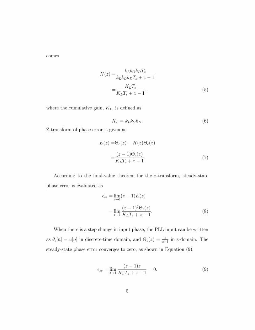
H(z) =kLkOkDTs
kLkOkDTs + z − 1
=KLTs
KLTs + z − 1, (5)
where the cumulative gain, KL, is defined as
KL = kLkOkD. (6)
Z-transform of phase error is given as
E(z) =Θc(z)−H(z)Θc(z)
=(z − 1)Θc(z)
KLTs + z − 1. (7)
According to the final-value theorem for the z-transform, steady-state
phase error is evaluated as
εss = limz→1
(z − 1)E(z)
= limz→1
(z − 1)2Θc(z)
KLTs + z − 1. (8)
When there is a step change in input phase, the PLL input can be written
as θc[n] = u[n] in discrete-time domain, and Θc(z) = zz−1
in z-domain. The
steady-state phase error converges to zero, as shown in Equation (9).
εss = limz→1
(z − 1)z
KLTs + z − 1= 0. (9)
5

When there is a step change in input frequency, the PLL input can be writ-
ten as θc[n] = 2π∆fcTsnu[n] in discrete-time domain, and Θc(z) = 2π∆fcTsz(z−1)2
in z-domain. The steady-state phase error converges to a constant, as shown
in Equation (10).
εss = limz→1
2π∆fcTsz
KLTs + z − 1=
2π∆fcKL
. (10)
For an ideal phase detector that has a linear range from −π2
toπ2, the
maximum frequency deviation allowed at the input is
|∆fc| <KL
4. (11)
A second-order loop PLL is obtained when L(z) is a first-order loop filter.
We examine the case where the loop filter is a proportional-integral (PI) filter,
which can be expressed as
L(z) = kL1 + αz−1
1− z−1, (12)
where kL and α are filter parameters. Substituting Equation (12) in Equation
(3), phase transfer function becomes
H(z) =kLkOkDTs(z + α)
z2 + (kLkOkDTs − 2)z + kLkOkDTsα + 1
=KLTs(z + α)
z2 + (KLTs − 2)z +KLTsα + 1(13)
Z-transform of phase error is given as
6

E(z) =Θc(z)−H(z)Θc(z)
=(z − 1)2Θc(z)
z2 + (KLTs − 2)z +KLTsα + 1(14)
Steady-state phase error is evaluated as
εss = limz→1
(z − 1)E(z)
= limz→1
(z − 1)3Θc(z)
z2 + (KLTs − 2)z +KLTsα + 1(15)
Then we follow the same logic to analyze the steady-state phase errors in
the presence of a step change in input phase and input frequency, respectively.
Results are presented in Equations (16) and (17).
εss = limz→1
(z − 1)2z
z2 + (KLTs − 2)z +KLTsα + 1= 0. (16)
εss = limz→1
(z − 1)2π∆fcTsz
z2 + (KLTs − 2)z +KLTsα + 1= 0. (17)
This second-order PLL has a lock range that goes to infinity since the
phase error always converges to zero.
2.2 Phase detector
Given the in-phase and quadrature (IQ) components of the input signal,
7

the phase of the signal can be computed as
ε[n] = arctan(Q[n]
I[n]), (18)
Figure 3 shows the block diagram of an ideal phase detector and Figure
4 shows the characteristics of an ideal phase detector that has a linear range
of (−π2, π
2). However, an arctan function is difficult to implement on FPGA
due to the limited resources and computation limits of the hardware. In
this section, we present two practical implementations of phase detectors on
FPGA and evaluate their performance.
2.2.1 Modified Costas phase detector
As discussed in [2], arctan(Q[n]I[n]
) can be replaced by its mathematically
equivalent sin−1( Q[n]√Q[n]2+I[n]2
). With small input phase, sin−1( Q[n]√Q[n]2+I[n]2
)
can be approximated by Q[n]√Q[n]2+I[n]2
. The expression√Q[n]2 + I[n]2 is the
square root of the input signal power and can be removed using Automatic
Gain Control (AGC). The Costas phase detector is expressed as ε[n] = Q[n].
The problem of this phase detector is that it has negative slope in the left-
half of the I-Q plane. To correct this, the sign of I[n] is added to flip the
phase detector output about the I axis in the left-half of the I-Q plane, and
then the equation can be given as
ε[n] = sgn(I[n])Q[n]. (19)
8

The gain of phase detector, kD, is defined as the phase detector output
divided by the input phase error. In this case, it is given as
kD =
√Pinsin(ε[n])
ε[n], (20)
where Pin is the input signal power and ε[n] is the input phase error. The
biggest problem for the Modified Costas phase detector is that kD depends
on the input phase error. This type of phase detector is not strictly linear. As
shown in Figure 5, the gain can be assumed roughly linear only when the in-
put phase error is small. This leads to some error in system characterization.
However, since the Modified Costas phase detector is a very computationally
efficient algorithm, it is widely used in FPGA applications.
2.2.2 CORDIC phase detector
The CORDIC algorithm is an iterative method to compute a wide range of
functions, including trigonometric, hyperbolic, and logarithmetic, using only
shift, add, and sign functions. It is employed in our project to implement
the arctan phase detector. Andraka described the theory of the CORDIC
algorithm being used in vectorizing mode in [3]. Below is the brief summary of
the theory and the evaluation of its performance using MATLAB simulation.
In short, the goal is to find the angle of a vector (x,y) given its coordinates
in a Cartesian plane. The CORDIC algorithm rotates the vector to align it
with the x axis, minimizing y. This is done with many iterative steps. At each
9

step, the sign of y indicates which direction to rotate next and z accumulates
the phase change. If it is initialized to zero, the final value will be the angle
of the original vector. Equations for implementation are given below:
xi+1 = xi − 2−iyidi (21)
yi+1 = yi + 2−ixidi (22)
zi+1 = zi − arctan(2−i)di (23)
where di = −sgn(yi), z1 = 0, x1 = x, and y1 = y. As a set of known values,
arctan(2−i) can thus be implemented with a look-up table.
The biggest limitation of the CORDIC algorithm is that there exist up-
per and lower bounds for the output phase. In other words, the CORDIC
algorithm output reaches a plateau after the input phase exceeds a certain
value. The bound is computed mathematically in Equation (24).
|z∞| =i=1∑i=∞
arctan(2−i) = 0.9579 (24)
Figure 6 shows the characteristic of the CORDIC phase detector imple-
mented with 6 iterations. With infinite iterations, the CORDIC phase de-
tector should be perfectly linear within the region specified by its upper and
lower bounds. The jaggedness that appears in Figure 6 is due to quantization
error and can be reduced by increasing the number of iteration cycles. As
shown in Figure 6, its phase detector gain kD is constant as long as the mag-
10

nitude of input phase error does not exceeds 0.9579 radians. To compute the
lock range for first-order PLL implemented with CORDIC phase detector,
Equation (11) should be modified to account for the clipping effect.
−0.9579 < εss =2π∆fcKL
< 0.9579 (25)
Then the lock range is given by
|∆fc| < 0.1525KL (26)
2.3 DDS theory
An Analog Devices AD9954 DDS, configured to operate in single-tone
mode, is used as the digital VCO in our project. This section summarizes
the theory of operation of AD9954 and analyzes its performance in PLL.
Discussion will focus on the aspects of AD9954 that pertain to the project.
As stated in [4], DDS is a technique for using digital data processing
blocks as a means to generate a frequency- and phase-tunable output signal
referenced to a fixed-frequency clock source. Figure 7 shows a generic block
diagram of DDS. To begin with, it is instructive to visualize the sine gen-
erator as a vector rotating around a phase wheel, as shown in Figure 8. A
revolution around the phase wheel corresponds to a cycle in a generated sine
wave. The content of the phase accumulator, referred to as phase register in
Figure 7, corresponds to the points on the phase wheel. At each system clock
11
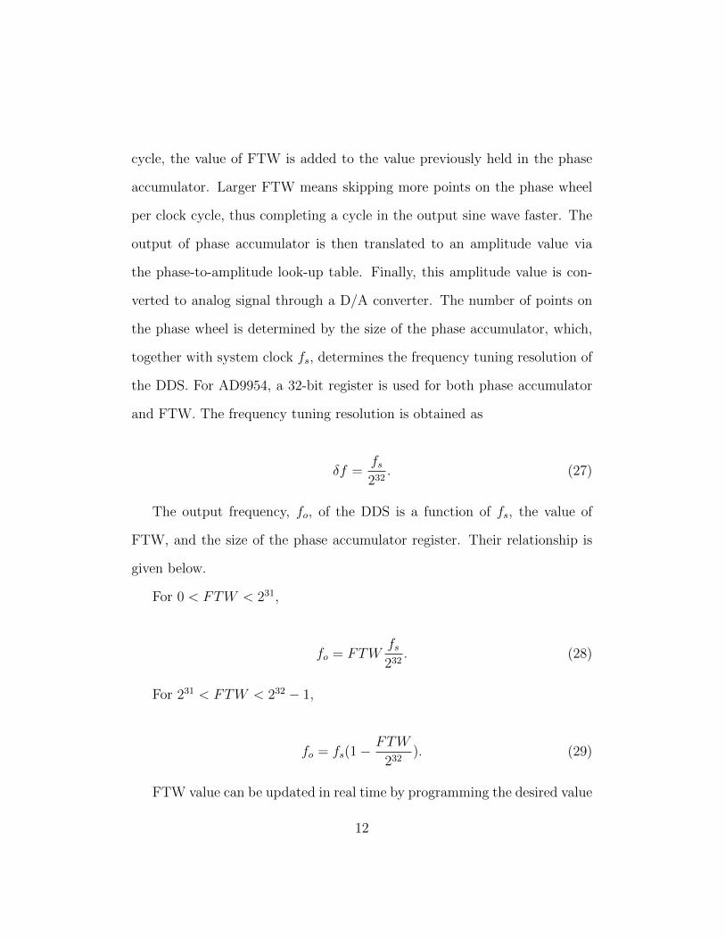
cycle, the value of FTW is added to the value previously held in the phase
accumulator. Larger FTW means skipping more points on the phase wheel
per clock cycle, thus completing a cycle in the output sine wave faster. The
output of phase accumulator is then translated to an amplitude value via
the phase-to-amplitude look-up table. Finally, this amplitude value is con-
verted to analog signal through a D/A converter. The number of points on
the phase wheel is determined by the size of the phase accumulator, which,
together with system clock fs, determines the frequency tuning resolution of
the DDS. For AD9954, a 32-bit register is used for both phase accumulator
and FTW. The frequency tuning resolution is obtained as
δf =fs232
. (27)
The output frequency, fo, of the DDS is a function of fs, the value of
FTW, and the size of the phase accumulator register. Their relationship is
given below.
For 0 < FTW < 231,
fo = FTWfs232
. (28)
For 231 < FTW < 232 − 1,
fo = fs(1−FTW
232). (29)
FTW value can be updated in real time by programming the desired value
12

into the FTW register via DDS serial I/O port. The AD9954 serial I/O is
compatible with most standard serial communication protocols, including
SPI, which is used in this project. This part is elaborated in Section 3.2.
In order to fit DDS into our PLL model, we need to characterize it in
discrete-time domain. The relation between two consecutive output phase
samples can be expressed as
θo[n+ 1] = θ[n] + 2π∆f [n]Ts, (30)
where ∆f [n] is DDS offset from free-running frequency at time n. Comparing
with Equation (1), ∆f [n] relates to c[n] by c[n]kO = 2π∆f [n]. In our project,
DDS is clocked with a 20 MHz external source and the internal system clock
is scaled to 400 MHz by a clock multiplier. Therefore, kO can be computed
as
kO = 2π400M
232= 0.5849. (31)
An intuitive way to interpret this result is that control signal c[n] = 1 corre-
sponds to a 0.5849 rad/s increase in DDS output angular frequency.
AD9954 features precise frequency control with a step size of 0.0931 Hz for
400 MHz system clock. It is robust against component aging and temperature
drift. The amount of output frequency jitter largely depends on the quality
of the reference clock. Any deviation in reference clock frequency will result
in magnified DDS output frequency deviation.
13

2.4 Figures
Figure 1: Generic discrete-time PLL
Figure 2: Linear model of discrete-time PLL
Figure 3: Ideal phase detector
14

Figure 4: Ideal phase detector characteristics
Figure 5: Modified Costas phase detector characteristics
15

Figure 6: CORDIC phase detector characteristics
Figure 7: Generic block diagram of DDS, cited from [4]
16

Figure 8: Phase wheel, cited from [4]
17

3 Implementation and Analysis
3.1 FPGA
3.1.1 NI 5640r hardware
NI 5640r is a very powerful IF transceiver that can be programmed with
LabVIEW graphical programming language. In this chapter, we will cover
the hardware components that are related to our project. More information
on NI PCI-5640r can be found in [5].
As shown in Figure 9, NI PCI-5640r has two analog inputs (AI) with
built-in digital downconverter(DDC), two analog outputs with built-in digital
upconverter (DUC), and seven digital I/O (DIO) lines. In our project, one
AI channel is used to receive the incoming signal at 10.7 MHz and five DIO
lines are used to communicate with the DDS. Incoming signal is sampled at
100 MHz at the front end of ADC and then converted to baseband IQ data
by DDC. IQ data can be processed directly on FPGA using inline processing
or streamed to host using Direct Memory Access (DMA) via PCI interface.
NI PCI-5640r has six available base clocks that can be used to control
the timing of the processes running on FPGA. Figure 10 shows the names
of each clock and Figure 11 shows how each is derived from the source. The
device reference clock that drives all base clocks except Configuration Clk
can be chosen from an internal VCXO of 200 MHz or an external clock.
18
Configuration Clk is the on-board clock used by PCI-DMA operation.
It is fixed at 20 MHz and is independent of other clocks. By default, the
majority of the functions on the FPGA that are not timed explicitly are
compiled to this clock so that their execution time stays constant when other
base clocks are customized to run at various frequencies.
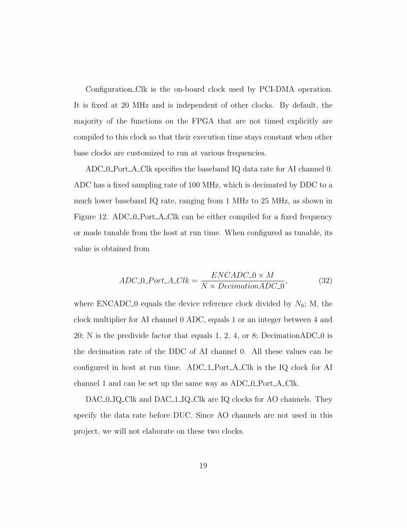
ADC 0 Port A Clk specifies the baseband IQ data rate for AI channel 0.
ADC has a fixed sampling rate of 100 MHz, which is decimated by DDC to a
much lower baseband IQ rate, ranging from 1 MHz to 25 MHz, as shown in
Figure 12. ADC 0 Port A Clk can be either compiled for a fixed frequency
or made tunable from the host at run time. When configured as tunable, its
value is obtained from
ADC 0 Port A Clk =ENCADC 0×M
N ×DecimationADC 0, (32)
where ENCADC 0 equals the device reference clock divided by N0; M, the
clock multiplier for AI channel 0 ADC, equals 1 or an integer between 4 and
20; N is the predivide factor that equals 1, 2, 4, or 8; DecimationADC 0 is
the decimation rate of the DDC of AI channel 0. All these values can be
configured in host at run time. ADC 1 Port A Clk is the IQ clock for AI
channel 1 and can be set up the same way as ADC 0 Port A Clk.
DAC 0 IQ Clk and DAC 1 IQ Clk are IQ clocks for AO channels. They
specify the data rate before DUC. Since AO channels are not used in this
project, we will not elaborate on these two clocks.
19

RTSI Ref Clk, like ADC 0 Port A Clk, can be either compiled as a fixed
frequency or as tunable from host. Its value is equal to the device reference
clock divided by N4, which can be 1, 2, 4, 8, or 16. This clock is usually
customized to be used to control the timing of FPGA programs because it is
configurable and will not affect other hardware functionality.
3.1.2 Main processing loops
We start this section with the introduction of some terminologies that
are widely used to describe LabVIEW FPGA programs. According to [6],
Direct Memory Access (DMA) is defined as a method by which one can
transfer data to computer memory from a device, also called target, or from
computer memory to a device, while the processor remains free for other
tasks. FIFO refers to block memory that implements a first-in-first-out data
exchange policy. Data to be transferred within FPGA can be stored in target-
scoped FIFO; data to be transferred between host and FPGA can be stored
in host-to-target DMA FIFO or target-to-host DMA FIFO depending the
transportation direction.
All digital signal processing is implemented on FPGA within three paral-
lel processing loops. The first loop is called the acquisition loop, as shown in
Figure 13, where IQ data are collected from analog input ports and written
into target-scoped FIFO. Phase detector is implemented in this loop. The
Boolean variable “CORDIC?” controls whether Modified Costas phase detec-
tor or CORDIC phase detector should be used in PLL. For every incoming
20

IQ pair, one phase error value is computed and stored in a local variable.
Then the phase error value is passed to the DIO loop to compute the con-
trol signal c[n]. But most of the phase error values will be discarded due to
the relatively slow execution rate of the DIO loop. The acquisition loop is
a single-cycle timed loop, which means its execution time can be precisely
controlled by the clock wired to the input node. In other words, the user can
slow down the processing rate by skipping samples, regardless of IQ clock
rate. In this case, the loop is clocked with ADC 0 Port A Clk at 1 MHz,
which means every IQ sample acquired is passed through for processing.
Figure 14 shows the data transfer loop, which simply moves data from
target-scoped FIFO to target-to-host DMA FIFO. Simple manipulation of
data, such as scaling, can be done in this loop sample-by-sample before they
are sent to the host. Host will access target-to-host DMA FIFO and retrieve
a large chunk of samples every time. This loop must run faster than the
acquisition loop to make sure that the target-scope FIFO does not overflow.
In our project, this loop is configured to run at 4 MHz.
The third loop is called DIO loop which encloses loop filter L(z) and the
DDS-FPGA interface. As mentioned before, IF-RIO has 7 digital output
lines, 5 of which are used for SPI communication with DDS. See Table 1 for
the pin descriptions.
According to DDS specifications, each communication cycle consists of
two phases. Phase 1 is the instruction cycle, which is the writing of an in-
struction byte, coincident with the first eight SCLK rising edges; phase 2 is
21

Table 1: DIO pin descriptionsPin number function
2 data line (SPI DOUT)3 reset (RESET)4 chip select (CS)5 serial clock (SPI SCLK)6 I/O update
1,7 not used
the actual data transfer between AD9954 and the system controller. The
number of bytes transferred during phase 2 of the communication cycle is a
function of the register being accessed. Most of the time, we only use the
FPGA-DDS interface to update FTW. In this case, the data packet consists
of 8 bits of instruction and 32 bits of FTW value. The following discussion
will be based on 40-bit data packet transfer. At the beginning of each com-
munication cycle, CS is asserted and the first bit in the data packet is loaded
on the data line, entering the WHILE loop. The WHILE loop consists of a
three-step sequence. The first step is intended to allow the data bit to sta-
bilize on the data line. In step 2, SCLK is set high and DDS starts to read
the data bit. SCLK is set low in step 3. The WHILE loop is repeated for
40 times. SCLK rate and duty cycle can be adjusted by changing the loop
timer value in step 1 and wait timer value in step 2. At the completion of a
communication cycle, I/O update is asserted to transfer internal buffer con-
tents into control registers on DDS. Then, CS, SPI DOUT, and I/O update
are set to idle state, waiting for the next communication cycle. The timing
diagram can be found in [7]. Figure 15 shows the implementation of the SPI
22

interface on LabVIEW FPGA. Figure 16 shows an oscilloscope acquisition of
FPGA digital output.
Precise time control of this loop is desirable but not possible because
single-cycle timed loop does not allow WHILE loop nested inside. Fortu-
nately, this does not cause a problem because FPGA programs, once com-
piled, will maintain deterministic execution as long as functions to be per-
formed require constant clock cycles. The WHILE loop placed without timing
defined will run on Configuration Clk of 20 MHz. This argument is supported
by experimental measurement of SPI SCLK. As shown in Figure 17, the du-
ration between two communication cycles, i.e. 40 SPI SCLK cycles followed
by an idle period, is repeatedly measured to be 35.1µs. From the perspective
of system characterization, FTW is updated once per 35.1 µs, meaning that
the sampling rate of the PLL is 135.1 µs
= 28.5 KHz, i.e Ts = 35.1 µs.
Three types of loop filters are implemented in this loop. Two of them
have been described in Section 2.1. The third one is a three-stage Cascaded
integrator-comb (CIC) filter which is introduced to exemplify a computa-
tionally efficient implementation of narrowband lowpass filter. It should be
noted that all quantitative analysis of second-order PLL in the following sec-
tions are based on PI filter. Since FPGA has limited computation ability,
all math related functions must be implemented with fixed-point arithmetic.
The size of each fixed-point variable must be carefully selected to strike a
balance between high throughput and precision. Figures 18, 19, and 20 show
the implementation of each loop filter, respectively.
23

3.2 Other hardware
A PCB-based crystal oscillator with 20 MHz output frequency is used as
the reference clock for AD9954 DDS. As described in [8], the oscillator circuit
consists of a Common-collector BJT in Colpitts configuration and another
BJT as emitter follower to match the output impedance to 50 Ω. A ceramic
filter centered at 10.7 MHz with a bandwidth of 200 KHz is used as IF filter.
It is soldered on the PCB with two L-networks that match its input and
output impedance to 50 Ω. Mini-Circuits ZP-3LH is the mixer that shifts
the input signal from 70 MHz to 10.7 MHz. An Agilent E3648A DC power
supply provides a +12 V DC voltage for BJTs in the crystal oscillator. This
voltage is stepped down to 3.3 V and 1.8 V by two low drop-out (LDO) linear
regulators to provide DC power for AD9954 DDS.
3.3 Modeling of actual system
In this section, we will analyze the actual system and characterize it using
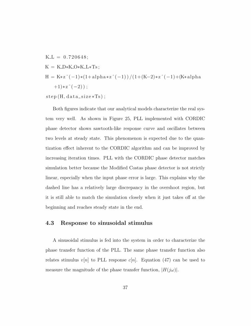
the theoretical model developed in Chapter 2. Figure 21 contains the block
diagram of the actual system.
Incoming analog signal is
x(t) = acos(2πfct+ θc(t)). (33)
It is mixed with the DDS output cos(2πfot + θo(t)) and shifted down to
24

intermediate frequency (IF) and then passed through a bandpass filter (BPF)
that cuts off high frequency components. It becomes
x′(t) = akmkfcos(2π(fc − fo)t+ θc(t)− θo(t)), (34)
where km is the attenuation in voltage of the mixer and kf is the attenuation
in voltage at the passband of the filter.
The signal then is digitized at IF-RIO analog input and converted to
baseband IQ data.
I[n] = akmkfkADCcos(2π(fc − fo − fNCO)nTs + . . .
+θc[n]− θo[n]− θNCO[n]), (35)
Q[n] = akmkfkADCsin(2π(fc − fo − fNCO)nTs + . . .
+θc[n]− θo[n]− θNCO[n]), (36)
where fNCO is the frequency of the Numerically-Controlled Oscillator (NCO)
that is embedded in the NI PCI-5640r AI channel. This value is configurable
from host in real time. In this case, it is set nominally to 10.7 MHz so that the
input signal is shifted from IF to baseband. θNCO is the phase of the NCO. We
define k = akmkfkADC and actual phase error is ε[n] = θc[n]−θo[n]−θNCO[n].
At steady state, when fc = fo + fNCO, Equations (35) and (36) can be
simplified as
25

I[n] = kcos(ε[n]) = kcos(ε[n]), (37)
Q[n] = ksin(ε[n]) = ksin(ε[n]). (38)
The phase detector outputs an estimate of the phase error,ε[n], the ac-
curacy depending on the range of input phase error and the type of phase
detector. For the Modified Costas phase detector, its output is given as
ε[n] = sgn(I[n])Q[n] = kDε[n], (39)
where
kD =ksin(ε[n])
ε[n], for − π
2+ nπ < |ε[n]| < π
2+ nπ, n ∈ Z. (40)
For the CORDIC phase detector, its output is given as
ε[n] =
kDε[n] if |ε[n]| < 0.09579
±0.09579kD else
, (41)
where
kD =215 − 1
π2
= 20860. (42)
26

3.4 Figures
Figure 9: Block diagram of NI 5640r, cited from [5]
27

Figure 10: FPGA base clocks, modified from [6]
Figure 11: IF-RIO clock resources, modified from [6]
28

Figure 12: Analog I/O channel block diagram, cited from [6]
Figure 13: Acquisition loop
29
Figure 14: Data transfer loop
Figure 15: SPI interface
30

Figure 16: Real-time display of FPGA digital output. Channel 1 is SCLK;Channel 2 is the data line.
Figure 17: Measurement of Ts
31

Figure 18: Constant gain
Figure 19: CIC filter
32
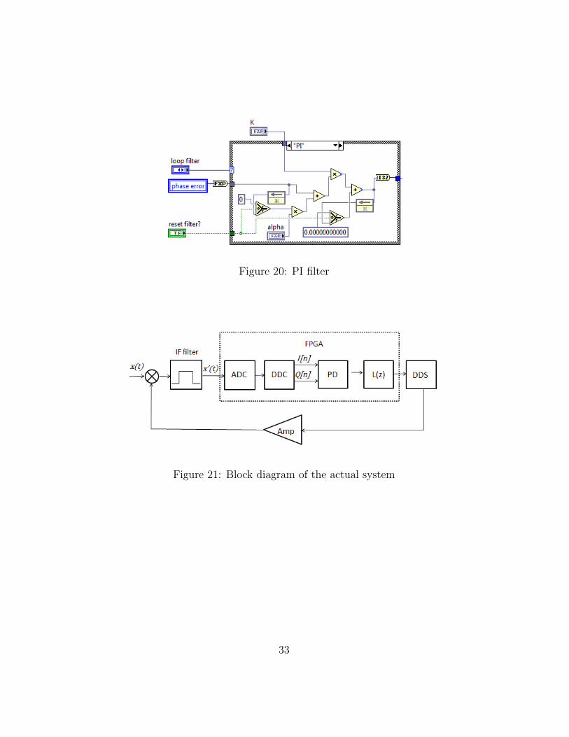
Figure 20: PI filter
Figure 21: Block diagram of the actual system
33

4 Experiment and Characterization
4.1 Constant parameters in experiment setup
A 0 dBm 70 MHz sine wave is used as the input signal. Then a = 12Vpp =
0.3168. Mixer conversion loss is measured to be 5.5 dB at 10.7 MHz, indi-
cating an input output voltage ratio of km = 0.53. IF filter insertion loss is
measured to be 2.8 dB at 10.7 MHz, indicating an input output voltage ratio
of kf = 0.725 at passband. According to [9], full-scale input range of the
NI PCI-5640r is 8.5 dBm at 10 MHz and baseband IQ data are represented
as signed 16-bit numbers. Therefore, kADC = 215−10.8414
= 38943. Combining all
aforementioned gains gives k = akmkfkADC = 4741, which will be used to
compute the gain of Modified Costas phase detector. According to Equations
(39) and (40), the output of the Modified Costas phase detector can be rep-
resented as ε[n] = sgn(I[n])Q[n] = ±akmkfkADCsin(ε[n]) = ±4741sin(ε[n]).
In Section 2.3 and Section 3.1, we have obtained kO = 0.5849 and Ts =
35.1 µs, respectively. Plugging in constants from different stages to Equa-
tions (5) and (13), the phase transfer functions of the actual system are
given as follows:
for first-order PLL with the Modified Costas phase detector,
H(z) =kLkOkDTs
kLkOkDTs + z − 1=
0.0968kLsin(ε[n])
0.0968kLsin(ε[n]) + z − 1; (43)
for first-order PLL with the CORDIC phase detector,
34

H(z) =kLkOkDTs
kLkOkDTs + z − 1=
0.4246kLsin(ε[n])
0.4246kLsin(ε[n]) + z − 1; (44)
for second-order PLL with Modified Costas phase detector,
H(z) =kLkOkDTs(z + α)
z2 + (kLkOkDTs − 2)z + kLkOkDTsα + 1,
=0.0968kLsin(ε[n])(z + α)
z2 + (0.0968kLsin(ε[n])− 2)z + 0.0968kLsin(ε[n])α + 1; (45)
for second-order PLL with CORDIC phase detector,
H(z) =kLkOkDTs(z + α)
z2 + (kLkOkDTs − 2)z + kLkOkDTsα + 1
=0.4246kLsin(ε[n])(z + α)
z2 + (0.4246kLsin(ε[n])− 2)z + 0.4246kLsin(ε[n])α + 1. (46)
4.2 Response to step stimulus
It is instructive to study the PLL response when it is subject to a step
change input in phase. As examined in Section 2.1, if the step deviation is
within lock range, PLL should be able to track the change after a transient
period, the length of which is determined by loop filter parameters.
The most intuitive way to measure the step response is to introduce a
known step change in the input signal and measure the phase response at
the output. However, this method requires measuring the input signal and
the PLL response in the same time domain. A two-channel VSA would be
able to carry out this task. Due to the lack of the above mentioned equipment,
we use an alternative but equivalent way to characterize it.
35

Figure 22 shows the block diagram of the experiment setup. A zero-offset
square wave stimulus with tunable amplitude is added to the control signal
c[n]. In a linear feedback system, this is equivalent to introducing a repeated
step change in the input frequency. The square wave frequency is chosen to
be as low as 14 Hz, so that PLL is guaranteed to reach steady state before
the next step change takes place. The control signal c[n] is measured as the
PLL response phase.
Figures 23 and 24 show a few measured curves with different choices of
loop filter type and parameters. Different kL are chosen for PLL implemented
with the Modified Costas PD and for PLL implemented with the CORDIC
phase detector to offset the effect of their different phase detector gains. As
a result, both PLLs have the same cumulative gain, KL, which is defined as
KL = kLkOkD . Measurement results are graphed together with their corre-
sponding MATLAB simulations to verify how well the models we developed
in the Section 3.3 describe the actual system. The following lines of code,
modified from [10], are used to generate the MATLAB simulation in Figure
24 for the second-order PLL.
d a t a s i z e = length ( measured data ) ;
Ts = 35 .1 e−6;
z = t f ( ’ z ’ , Ts ) ;
alpha = −0.994036
K D = 4741 ;
K O = 0.5849
36
K L = 0.720648 ;
K = K D∗K O∗K L∗Ts ;
H = K∗zˆ(−1)∗(1+ alpha∗zˆ(−1) ) /(1+(K−2)∗zˆ(−1)+(K∗alpha
+1)∗zˆ(−2) ) ;
s tep (H, d a t a s i z e ∗Ts) ;
Both figures indicate that our analytical models characterize the real sys-
tem very well. As shown in Figure 25, PLL implemented with CORDIC
phase detector shows sawtooth-like response curve and oscillates between
two levels at steady state. This phenomenon is expected due to the quan-
tization effect inherent to the CORDIC algorithm and can be improved by
increasing iteration times. PLL with the CORDIC phase detector matches
simulation better because the Modified Costas phase detector is not strictly
linear, especially when the input phase error is large. This explains why the
dashed line has a relatively large discrepancy in the overshoot region, but
it is still able to match the simulation closely when it just takes off at the
beginning and reaches steady state in the end.
4.3 Response to sinusoidal stimulus
A sinusoidal stimulus is fed into the system in order to characterize the
phase transfer function of the PLL. The same phase transfer function also
relates stimulus v[n] to PLL response c[n]. Equation (47) can be used to
measure the magnitude of the phase transfer function, |H(jω)|.
37

|H(jω)| = |C(jω)
V (jω)|. (47)
The experiment setup is similar to the one used in Section 4.2 except
that the stimulus is replaced with a sinusoidal wave generator, which, im-
plemented on FPGA, is simply a look-up table consisting of two periods of
sinusoid pattern. The table size is 1024. The frequency of the sine stimulus
can be represented as nfs512
, where n is the iterator step size, which can be
controlled from host, and fs is the sampling frequency of the PLL. There
are two conditions for n: first, it has to be an integer since it corresponds to
the look-up table address; second, it has to be relatively small since skipping
too many samples leads to severely deformed output waveforms. An obvious
drawback of this method is that the total number of realizable frequency lev-
els is limited. The NI FPGA offers an option to linearly interpolate between
look-up table entries if the input address is a noninteger. But this is not
practical in our system. As mentioned in Section 3.1.2, the sampling fre-
quency of PLL is determined by the execution rate of the WHILE loop that
encloses the loop filter and FPGA-DDS interface. The timing of this loop is
not precisely controlled by any system clocks. Therefore, its execution rate
will be consistent only if every process inside this loop uses constant clock
cycle to execute. However, the execution time of an interpolation-enabled
look-up table varies depending on address input: it takes one clock cycle for
integer addresses and at least two clock cycles for noninteger addresses when
38

interpolation is needed. Nonuniform sample intervals of PLL will result if
the look-up table is operating in interpolation mode.
Figures 26 and 27 show measured phase transfer function curves for first-
order and second-order PLL, respectively, graphed with MATLAB simula-
tions. Data are collected at low frequencies for the reasons mentioned above.
4.4 Processing lag
The experiment described in Section 4.2 can also be used to measure
FPGA processing lag. It can be seen in Figures 28 and 29 that PLL starts
to respond to step stimulus after two samples. Thus processing delay can be
calculated as
τ = 2Ts = 2× 35.1µs = 70.2µs. (48)
Processing delay is inherent to all digital systems. In this case, it is
determined by the amount of operations performed on FPGA and the FPGA
processing speed. To make our system model more accurate, we have to
account for this delay by grouping it with the cumulative gain KL = kLkOkD.
For the first-order PLL, the phase transfer function becomes
H(z) =z−2KLTs(z + α)
z2 + (z−2KLTs − 2)z + z−2KLTsα + 1
=KLTsz
−3 + αz−2KLTsz−4
1− 2z−1 + z−2 +KLTsz−3 +KLTsαz−4(49)
39
We redo the step response simulation in MATLAB with the modified
phase transfer function. As before, the same parameters are used to facilitate
comparison of the two simulations. Simulations of both system functions
are graphed together with measurement data in Figure 30. As shown in
Figure 31, the simulation of the modified phase transfer function has smaller
discrepancy with the measurement data.
4.5 Lock range
In this section, we will present experimental measurement results of the
lock range of different types of PLLs and evaluate how well these values agree
with the theoretical calculation given in Section 2.1.
For PLL with the Modified Costas PD, kL = 0.6. The critical condition
for lock-in status is that the magnitude of steady-state phase error equals π2.
Substituting Equation (40) in Equation (11), we obtain
|∆fc| =ksin(π
2)kOkL
π2· 4
= 264.8 Hz (50)
The lock range was measured to be from −259.2 Hz to 257 Hz, which
agrees with Equation (50) with a 1.8% error.
For PLL with the CORDIC PD, kL = 0.14. The largest frequency offset
that can be tolerated in the PLL before losing lock is given as
|∆fc| = 0.1525KL = 0.1525kDkOkL = 260.5 Hz. (51)
40

The experimental result indicates a lock range from −257.6 Hz to 256.2 Hz,
which agrees with Equation (51) with a 1.5% error.
The statement we made in Section 2.1 that second-order PLL has infinite
lock range has been verified by experiment. In a real system, the limiting
factors that prevent the lock range going to true infinity are the sampling
rate of the system and the size of the register that holds the control signal
c[n].
41

4.6 Figures
Figure 22: Step response block diagram
Figure 23: The step response of first-order PLL
42

Figure 24: The step response of second-order PLL
Figure 25: Zoom-in of Figure 24
43

Figure 26: Magnitude of phase transfer function of first-order PLL
Figure 27: Magnitude of phase transfer function of second-order PLL
44
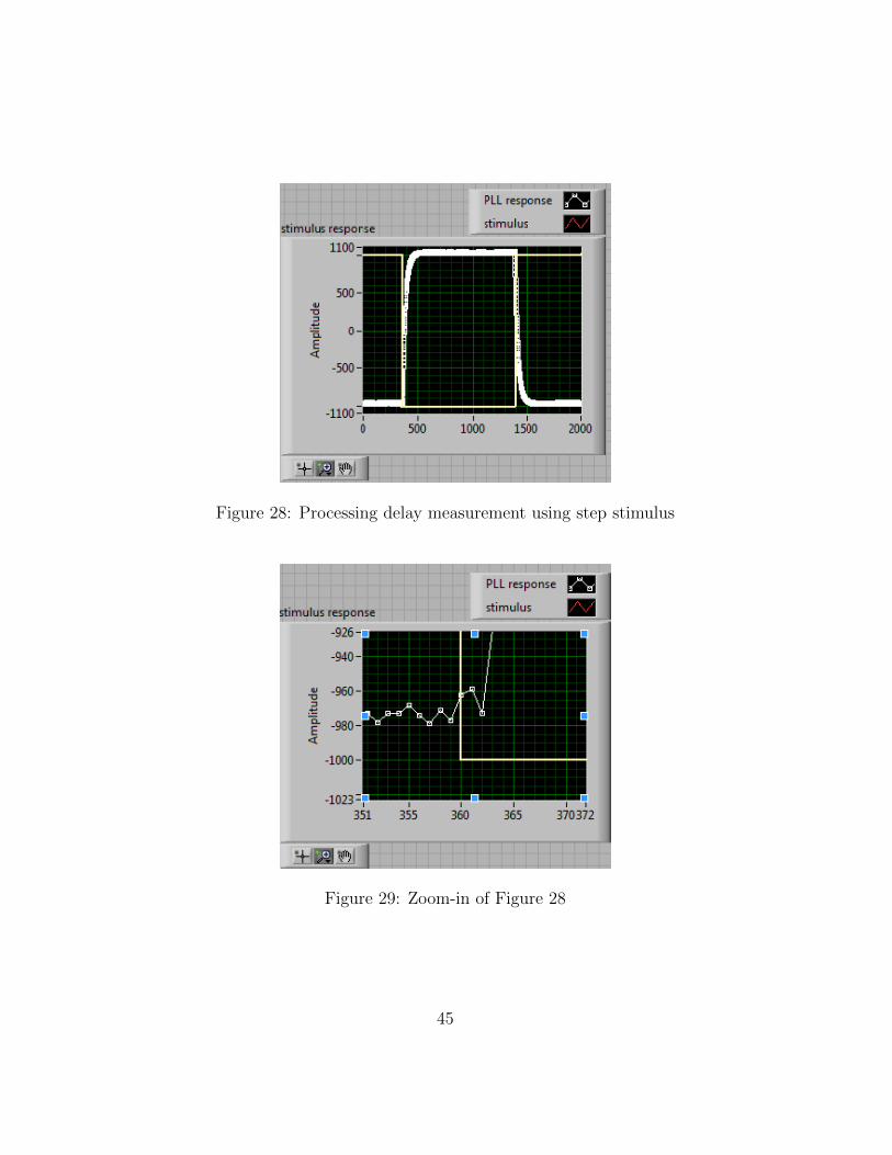
Figure 28: Processing delay measurement using step stimulus
Figure 29: Zoom-in of Figure 28
45

Figure 30: Step response of second order PLL with modified phase transferfunction
Figure 31: Zoom-in of Figure 29
46

5 Conclusion
The thesis presents a working digital PLL with two types of phase detectors
and three types of loop filters. This project is based on the NI PCI-5640r
and programmed with LabVIEW. The AD9954 DDS, used as a digital VCO,
is interfaced with the FPGA of the NI PCI-5640r via serial I/O. The system
is characterized numerically with in-lab measurements, the results of which
are compared with theoretical models to verify that the PLL operates as
expected.
This project will serve as a lab module for ECE 463 in the future. It
can be used in a transmitter to generate stable carrier frequencies and in
a coherent receiver to recover the carrier of the input signal. Furthermore,
the FPGA-DDS interface developed in this project provides a convenient
platform for future research efforts that involve the usage of DDS. DDS can
be easily controlled by programming or in real-time with LabVIEW and the
NI PCI-5640r.
47

References
[1] B. Farhang-Boroujeny, Signal Processing Techniques for Software Ra-dios. Salt Lake City, UT: University of Utah, 2008.
[2] Schmitz, C. (2010, February 23). Phase Detectors. Retrieved from theConnexions Web site: http://cnx.org/content/m14493/1.7/
[3] Ray Andraka, “A survey of CORDIC algorithms for FPGA based com-puters,” in Proceedings of the 1998 ACM/SIGDA sixth internationalsymposium on Field programmable gate arrays, 1998, pp. 191-200.
[4] Analog Devices Technical Staff, A Technical Tutorial on Direct DigitalSynthesizer, Analog Devices, Inc., 1999.
[5] National Instruments Technical Staff, Getting Started with the NI PCI-5640r IF Transceiver and the LabVIEW FPGA Module, National In-struments, 2006.
[6] National Instruments Technical Staff, NI IF Tranceivers Help, NationalInstruments, 2010
[7] AD9954 Data Sheet Rev B, Analog Devices,Inc., 2009
[8] S. J. Franke, Wireless Communication Systems. Class notes for ECE453, Department of Electrical and Computer Engineering, University ofIllinois at Urbana-Champaign, 2011.
[9] NI PCI-5640R Specifications, National Instruments, 2007.
[10] C. D. Schmitz, Phase-Locked Loops: Digital PLL, Loop Controller De-sign. Class notes for ECE 463, Department of Electrical and ComputerEngineering, University of Illinois at Urbana-Champaign, 2011.
48


