
3D sequential integration:
an alternative path towards CMOS scalability
FDSOI
FinFET
1

Outline
What is 3D sequential integration?
Why 3D sequential integration?
Key technological modules
2

Outline
What is 3D sequential integration?
Why 3D monolithic integration?
Key technological modules
3
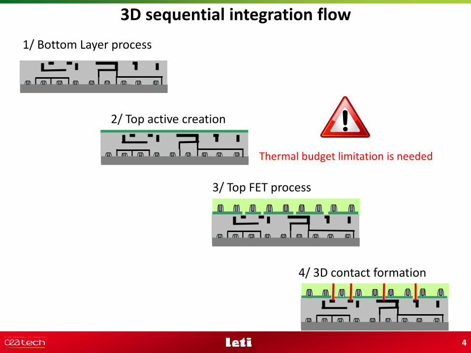
1/ Bottom Layer process
2/ Top active creation
4/ 3D contact formation
3D sequential integration flow
3/ Top FET process
4
Thermal budget limitation is needed

Difference with 3D packaging
Packaging integration (e.g: TSV ) Sequential integration
1/ Wafers processed separately
2/ Stacking and contacting
1/ Bottom Layer process
2/ Top layer process
3/ 3D contact formation
| 5
Packaging integration: stacked MOSFETs processed in separatlySequential integration: stacked MOSFETs processed sequentially

Packaging integration (e.g: TSV ) Sequential integration
Two reasons for the high 3D contact pitch: - Alignment performance- 3D contact process
3D sequential integration: advantage & challenge
3D TSV contact pitch 3-8µm3D contact density 104 -105 /mm2
3D contact pitch <100nm3D contact density > 108 /mm2
Major asset: Highest 3D contact density
Major challenge: Process top MOSFET at low thermal budget
6

Alignment performance with sequential 3D
[2]
Sequential 3D: alignement obtained by lithography. Litho stepper capability ~ 3σ=5nmPackaging 3D:alignment made during bondingBonding stepper capability 3σ~ 1µm
SEQUENTIAL 3D
Blanket top active Standard lithography
PACKAGING3D
Bonding of patterned filmsAlignment & bonding at the same time
~µm
~nm
[2] P. Batude et al., VLSI 2011
[1]
[1]
[1] www.besang.com 7
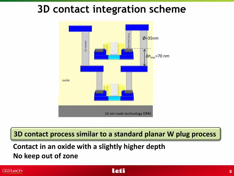
3D contact integration scheme
Contact in an oxide with a slightly higher depthNo keep out of zone
Δhmin=70 nm
Ø=35nm
14 nm node technology DRM
3D contact process similar to a standard planar W plug process
8

[3,4]: P. Garrou et al., Handbook of 3D integration, Vol 1,2 (Wiley ed) / [5]: B. Banijamali, ECTC2011[6]: S-M. Jung et al., VLSI 2005 pp220 / [7]: P. Batude et al, ECS journal 2008, VO16,pp47
3D contact density
65nm node
[3,4]
[6]
[7] D=5x10⁶/mm2
193 nm stepper
D=Density = Number of 3D contacts per mm2
0.01 0.1 1 10
0.01
0.1
1
10A
lig
nm
en
t accu
racy (
µm
)
3D contact width (µm)
SOI TOV
BULK TSV
Packaging
[5]
Sequential
D> 108 /mm 2
D= 105 /mm 2
D= 104 /mm 2
14nm node
9

Parallel 3D
Sequential 3D
GranularityGranularity scalescale
1-Entire core 2-Logic bloc 3-Logic gates 4-Transistors
3D sequential
Partitioning levels
3D packaging
10

Outline
What is 3D sequential integration
Why 3D sequential integration
1-Road map driven by FET performance
2-Road map driven by interconnection delay reduction
3-Opportunities of heterogeneous cointegration
Key technological modules
11

1- Roadmap driven by FET performance
12

1- Roadmap driven by FET performance
28FDSOI
28nm 14nm 10nm 7nm …
14FDSOI
Electrostatic: Non
planar/trigate
10FDSOI
2012 2014 2016 2018 2020
Mobility boostFinfet
Performance boosters are different for N &PFETs
Independant N&P optimization is easier with P/N stacking
13

Enable to choose the best - Material for each transistor
- Gate stack
- Strain
- Orientation
- Architecture
-
[1]: P. Batude et al., VLSI 2009
N/P configuration: boosting FET performance
[1] [2]
[1]
[2]
[2]: P. Batude et al., IEDM 2009 14

The ultimate cointegration III-V and (Si)Ge
nFET III-V and pFET Ge process are highly different:
Dual active etching/ Dual Gate stack/ Dual RSD/ different optimum architecture/ Dual salicidation/Substrate fabrication: dual material (epi with ART or III-V bonding on GeOI)…
T. Irisawa et al., VLSI 2013 (AIST)
Processing independantly n&pFET on distinct levels enable to save a lot of lithography levels and process co-integration challenges.
Additionnaly, III-V and Ge transistorsrequires lower thermal budget process.These devices are well adapted to 3Dsequential integration.
15

ex 1
ex 2 FDSOI
FinFET
Choice of architectures
For bottom level, every existing technology can be used
On top level, all the thin film technology can be used
16

Parallel 3D
Sequential 3D
GranularityGranularity scalescale
1-Entire core 2-Logic bloc 3-Logic gates 4-Transistors
Partitioning levels
Packaging 3D
N/P or P/ N stacking
IC Gain obtained by boosting FET performance
Sequential 3D
17
2- Roadmap driven by interconnection delay
18

2- Roadmap driven by interconnection delay
IC’s performance are strongly limited by interconnection delay
M. Sellier, et al., ISQED 2008
Wirelength must be reduced to benefit from gate delay reduction
19

Parallel 3D
Sequential 3D
GranularityGranularity scalescale
1-Entire core 2-Logic bloc 3-Logic gates 4-Transistors
Partitioning levels
Packaging 3D
CMOS/ CMOS stacking
IC Gain obtained by decreasing wirelength
Sequential 3D
20

CMOS/ CMOS option: Reducing wirelength
L1
1 2
L2
2
1
The 3D contact links blocks of MOSFETs
To avoid routing congestion, introduction of intermediatelines is mandatory
21

PPA gain thanks to wirelength reduction
Top metal layers
local interco W
Metal lines Cu et low-k
3D contact
Study taking into account parasitics / 3 metal line between the 2 stacked layers
Partitioning SRAM memory on bottom level, logic on top
Case of FPGA circuit
14nm planar FDSOI versus 2 stacked 14 nm FDSOI levels
Interlevel metal lines in W
No low k dielectrics
O. Turkylmaz et al. to DAC 2014 22
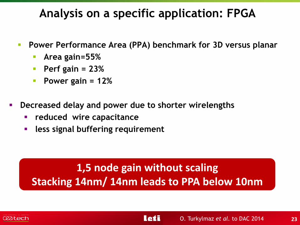
Decreased delay and power due to shorter wirelengths
reduced wire capacitance
less signal buffering requirement
Power Performance Area (PPA) benchmark for 3D versus planar
Area gain=55%
Perf gain = 23%
Power gain = 12%
Analysis on a specific application: FPGA
O. Turkylmaz et al. to DAC 2014
1,5 node gain without scalingStacking 14nm/ 14nm leads to PPA below 10nm
23
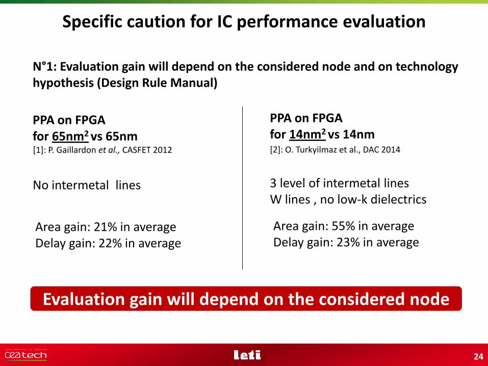
N°1: Evaluation gain will depend on the considered node and on technologyhypothesis (Design Rule Manual)
Specific caution for IC performance evaluation
PPA on FPGAfor 65nm2 vs 65nm
No intermetal lines
PPA on FPGAfor 14nm2 vs 14nm
3 level of intermetal linesW lines , no low-k dielectrics
Area gain: 21% in averageDelay gain: 22% in average
Area gain: 55% in averageDelay gain: 23% in average
[1]: P. Gaillardon et al., CASFET 2012 [2]: O. Turkyilmaz et al., DAC 2014
Evaluation gain will depend on the considered node
24

N°2: No place & route (P&R) tool adapted for 3D
Results provided only for FPGA thanks to it’s regular architecture that can
be achieved with full custom layout
P&R tool enable to optimize the position of the cells to obtain the best
gain (in term of area, timing or power)
Preliminar evaluation via « DIY » P&R tools
Specific caution for IC performance evaluation
Bottom cell
Top cell
S.Bobba et al., ASPDAC 2011
Planar configuration 2D to 3D transformation
Reliable conclusion can’t be provided without dedicated 3D P&R tool
25

Evaluation for ASiCs
45nm node/ 1 intermediate level only / with 2D modified P&R tool
S.Bobba et al., ASPDAC 2011
N°3: PPA Gain will highly depend on the application
Gain depends on the application
26

2- Roadmap driven by interconnection delay : Conclusion
Evaluation on FPGA is feasible thanks to its regular design (Full custom layoutpossible).
FPGA with two 14 nm stacked levels should enable to outperform the 10nm
Stacking more efficient than scaling?
No modification of transistor technology (tool reuse)
Gain obtained only due to wirelength reduction
27

Specific cautions to make a proper PPA benchmark:
# 1: Evaluation for other ICs cannot be properly performed due to the lack of 3D P & R tool work with EDA providers is necessary
#2: The results will greatly depend on the IC (predominance of delay in interconnection delay in the full IC performance)
#3: The result will greatly depend on the considered node(predominance of delay in advanced nodes)
#4: Technology assumptions must be analyzed carefully, particularly the number of intermediate lines authorized as well as the metal and dielectrics chosen.
2- Roadmap driven by interconnection delay : conclusion
28

3- A key technology for heterogeneous co-integration
Advantages of 3D
Independant optimisation of each level
Proximity between stacked functions
Only 3D sequential technology available if 3D contact pitch is smallerthan 1µm
29

Concept: Vertical dissociation of basic pixel operations
Pixel (x,y)
electrons
voltage
photons
Vpixel(x,y)
Y A
dd
ress
ing
X AddressingADC / CDS
2D 3DLight
pixel
Photodiode
Readout
Addressing& Processing
Pixel
Advantages of 3D configuration: Photodetection dedicated material and processes, 100% fill factorReadout transistors optimized process, relaxed geometriesSignal Processing Massively parallel treatment, dense IC integration
Suntharalingam et al., ISSCC 2005
3D integrated CMOS Image Sensors (3D-CIS)
Contribution from P.Coudrain from ST micro 30

TG Pinned
photodiode
Sensing
Node
-Detection-
RST
SF
READ
-Readout-
SOI 2-3 m
ILD
SOI 30nm
3D contacts
PMD
-10
0
10
20
30
40
50
0,1 0,2 0,3 0,4 0,5Dio
de a
rea incre
ase
(%
)3D contact diameter (μm)
1.4µm pitch
pixel
Multiple benefits
• BSI integration high quantum efficiency
• Photodiode area +44% for 1.4µm pitch pixel
Only sequential integration can address these
dimensions
Innovative miniaturized 4T pixels with backside illumination (BSI)[24]
• Bottom layer: pinned photodiode + Transfer Gate
• Top layer with 3 transistors
P.Coudrain et al., IEDM 2008
Miniaturized 3D CMOS Image Sensors
Contribution from P.Coudrain from ST micro 31

The challenge of detecting NEMS resonance: NEMS-CMOS integration schemes
Stand-alone NEMS + off-chip CMOS No density (pads number limitation)Very strong signal attenuation (LP filter)
3D sequential NEMS-CMOS No density limitationno signal attenuation
3D sequential integration of NEMS with CMOS
NEMs = ultra sensitive mass sensors used for gas sensing & mass spectroscopy
MEMS NEMS enable to increase the sensivitybut resonance detection is more complex
Contribution of J. Arcamone from leti
3D sequential NEMS-CMOS co-integration can solvethe NEMS density and detection limitation
32

Moving to NEMS array: i.e each NEMS is individually addressed.
Multiple benefits: increased robustness (redundancy), better SNR (averaging NEMS individual response, provide a spatial response (like an imager), ultra-high density to improve capture efficiency (smaller concentration detection)
3D sequential integration of sensors with CMOS
Analog CMOSsustaining electronics
NEMS plane
CMOS plane
Analog CMOSsustaining electronics
NEMS plane
CMOS plane
n-2 rows
m-1columns
CMOS planeFrequency counter
Vdd Vss
NEMS addressing
At this scale, only 3D sequential integration enable to reach the 3D contact pitch required (NEMS dimensions converge towards CMOS transistors)
Easy integration of NEMS thanks to it low thermal budget.
Rmk: same benefits applicable to other domains such as NEMS-based logic
NEMS array enables novel NEMS-based applications such as mass spectrometry
3D sequential is well adapted for NEMS array
33
Outline
What is 3D sequential integration
Why 3D sequential
1-Road map driven by FET performance
2-Road map driven by interconnection delay reduction
3-Opportunities of heterogeneous cointegration
Key technological modules
1-Maximum top layer thermal budget determination
2-Top active creation
3-Top FET at low temperature process
34

General Integration Flow
Bottom FET process Low temperatureTop active layer
Low temperatureTop FET process
Which thermal budget?
35
1- Maximum top FET thermal budget determination
Part III - Key technological modules
36

Standard FET process TB : up to 1000- 1100°C
Standard FET stability:400°C i.e temperature of BEOL process
Making 3D sequential integration possible
37
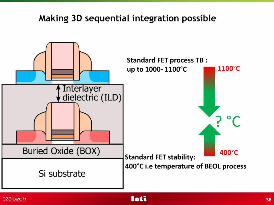
Standard FET process TB : up to 1000- 1100°C
Standard FET stability:400°C i.e temperature of BEOL process
Making 3D sequential integration possible
1100°C
400°C
? °C
38
Bottom FET stability
• Simple method: Annealing of a transistor and observe what
is the critical thermal budget for preserving its performance
• This critical thermal budget will depend of the technology
(BULK, FINFET, FDSOI) and the node analyzed
C. Fenouillet-Beranger et al, ESSDERC 2014 39

FDSOI with implanted Si RSD stability
C. Fenouillet-Beranger et al, ESSDERC 2014
FDSOI with implanted RSD: max thermal budget = 500°C
40

• No impact of the different anneals shown on multiple key electrical parameters such as:
• DIBL, short channel mobility evidencing no additional dopant diffusion
• EOT regrowth and reliability (NBTI & PBTI) evidencing good stability of the gate stack
FDSOI with implanted Si RSD stability
C. Fenouillet-Beranger et al, ESSDERC 2014 41
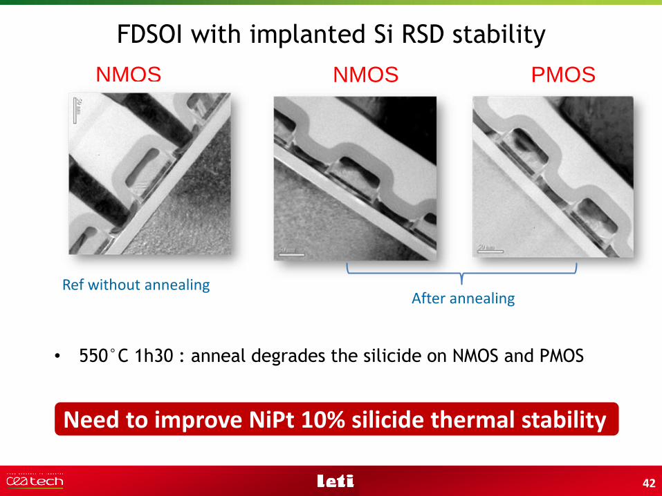
• 550°C 1h30 : anneal degrades the silicide on NMOS and PMOS
NMOS PMOSNMOS
Ref without annealing
FDSOI with implanted Si RSD stability
Need to improve NiPt 10% silicide thermal stability
After annealing
42

Bottom FET stability
P. Batude et al., IWJT 2013
NiPt silicidation associated with W offers higher thermal stability
43

Bottom FET stability
Techno 1: FDSOI [1]-Si channel-Si RSD and implanted source & drain-NiPt 10% salicidation Performance degradation above 500°C,5h
[2] C. Fenouillet- Beranger et al., IEDM 2014
Weak point of MOSFET technologies is salicide stability
Improving salicide stability could relax top FET maximum thermal budget
Techno 2: FDSOI with additional boosters [2]-Si channel for NFET, SiGe for pFET-SiGe:B & SiC:P in situ doped source & drain-NiPt 15% salicidationNo Performance degradation up to 550° 2h & 500°C 5h
Most secure criteria: max thermal budget= 500°C (5h)
[1] C. Fenouillet- Beranger et al., ESSDERC 2014 44
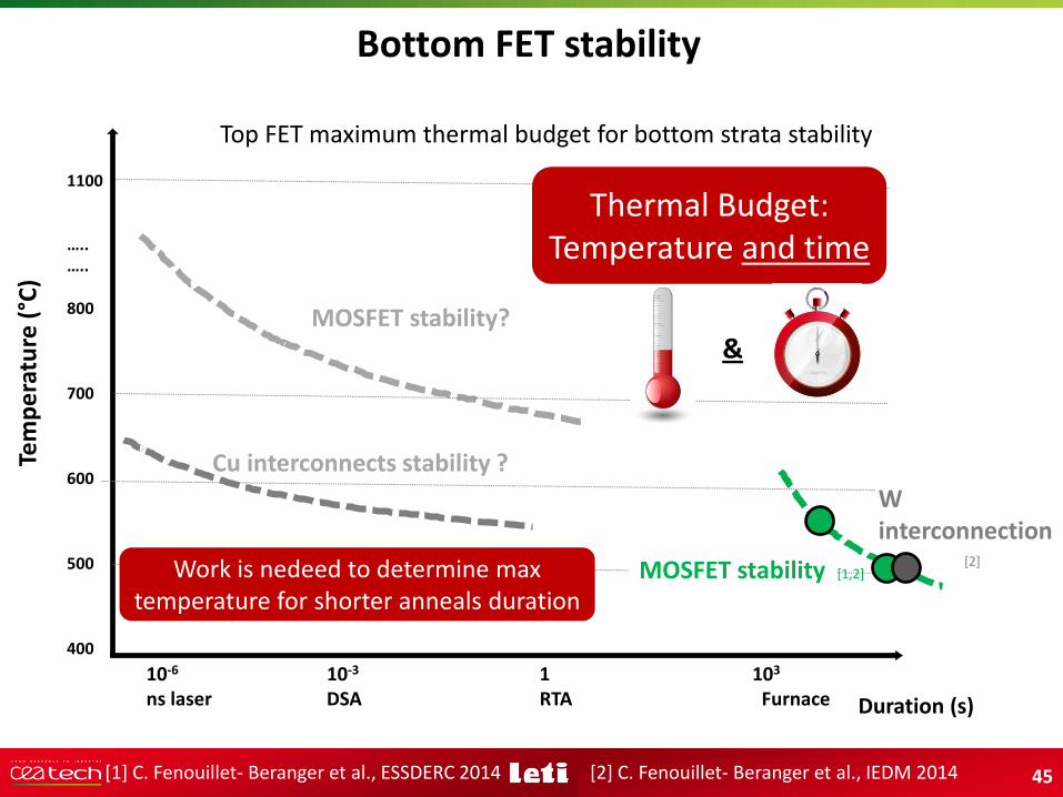
Tem
pe
ratu
re(°
C)
10-6 10-3 1 103
ns laser DSA RTA Furnace
Cu interconnects stability ?
1100
…..…..
800
700
600
500
400
MOSFET stability?
Top FET maximum thermal budget for bottom strata stability
Duration (s)
Bottom FET stability
Thermal Budget: Temperature and time
[1,2]MOSFET stability
[2] C. Fenouillet- Beranger et al., IEDM 2014[1] C. Fenouillet- Beranger et al., ESSDERC 2014
W interconnection
[2]
&
45
Work is nedeed to determine max temperature for shorter anneals duration
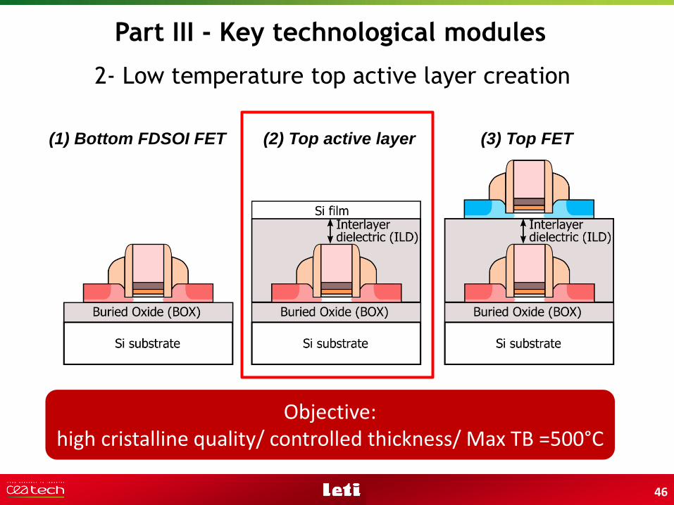
2- Low temperature top active layer creation
Part III - Key technological modules
(1) Bottom FDSOI FET (2) Top active layer (3) Top FET
Objective:high cristalline quality/ controlled thickness/ Max TB =500°C
46

Cristallization of amorphous Silicon
Finding solutions to increase the size of the grains at
temperature compatible with bottom MOSFET integrity
Amorphous silicon Poly silicon
47
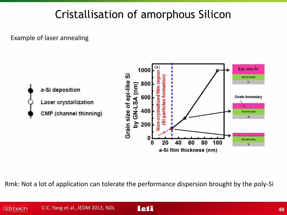
Cristallisation of amorphous Silicon
C-C. Yang et al., IEDM 2013, NDL
Example of laser annealing
Rmk: Not a lot of application can tolerate the performance dispersion brought by the poly-Si
48

“Seed window” techniques
To obtain the control of the grain boundaries position and grain orientation
SW
Cri
stal
line
info
rmat
ion
tra
nsf
er
49

Epitaxy Epitaxy
Lateral epi~650°C, min
amorphous deposition
thermal anneal (600°C,h)
c-Si
c-Si c-Si
a-Si
c-Si
Lateral epitaxy Solid Phase recrystallization
SiO2 SiO2
Liquid Phase recrystallization
Epitaxy
amorphous deposition
laser local fusion (ns)
c-Si
a-Si
c-Si
SiO2
“Seed window” techniques
S-M. Jung et al., VLSI 2007 Y-H. Son et al., VLSI 2007Liu et al., IEDM 2010
Remark: Too high thermal budgets applied to the bottom MOSFET
50
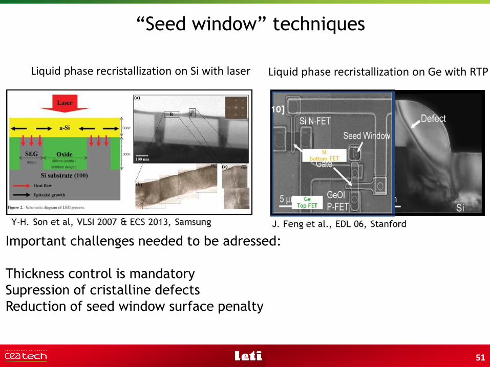
Important challenges needed to be adressed:
Thickness control is mandatory
Supression of cristalline defects
Reduction of seed window surface penalty
“Seed window” techniques
Liquid phase recristallization on Si with laser Liquid phase recristallization on Ge with RTP
51
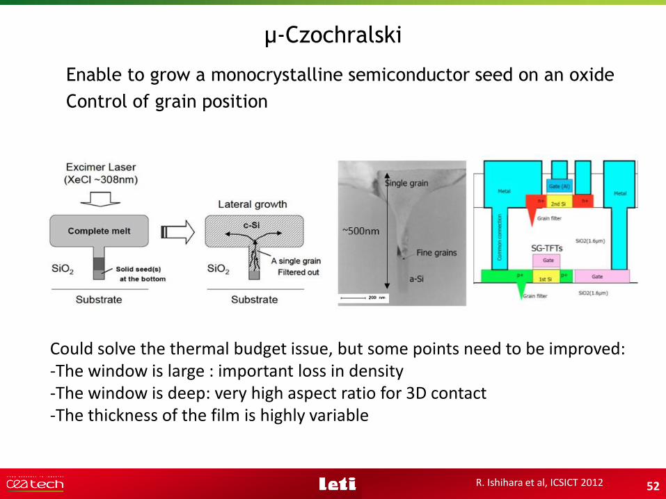
µ-Czochralski
Enable to grow a monocrystalline semiconductor seed on an oxide
Control of grain position
R. Ishihara et al, ICSICT 2012
Could solve the thermal budget issue, but some points need to be improved:-The window is large : important loss in density-The window is deep: very high aspect ratio for 3D contact-The thickness of the film is highly variable
52

Carbon nanotubes
Decoupling high temperature CNT growth and 3D sequential integration
H. Wei et al., IEDM 2009 53

Hydrophilic bonding Thermal anneal (200°C)
Si
CMP planarization
Si
SiBonding
interface
BULK
Bulk
Bonding
interface
Splitting200-500°C
SiO2
Hydrophilic bonding Thermal anneal (200°C)
H+ implant
BULK direct bonding and ion slicing
54

Examples of ion slicing reports on bottom MOSFET level
F. Crnogorac et al., JVSTB 2010, Stanford
D-S. Yu et al., IEDM 2004, Nat'l Chiao-Tung Univ, Taiwan L. Xue et al., TED 2003, Cornell university
Patterned reports might be due to:
-Non perfect CMP
-Bonding done with deposited oxide (whichcontains H20), patterning avoid the defectdue to degassing Solutions described in the following slides
55

Hydrophilic bonding Thermal anneal (200°C)
Si
Selectiveetching
CMP planarization
BOXSi
BOXSiBonding
interface
BOX
Si
BOXSiBonding
interface
Grinding
SiO2
SOI direct bonding
Hydrophilic bonding Thermal anneal (200°C)
56

Blanket Si film on top of a bottom transistor layer:
Stack cross section Top view: Acoustic characterization:
Full transfer on processed 300 mm wafers
High quality top film
57

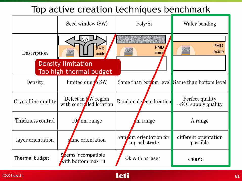
Top active creation techniques benchmark
Seed window (SW) Poly-Si Wafer bonding
Description
Density limited due to SW Same than bottom level Same than bottom level
Crystalline quality Defect in SW region
with controlled location Random defects location
Perfect quality ~SOI supply quality
Thickness control 10s nm range nm range Å range
layer orientation same orientation random orientation for
top substrate different orientation
possible
References [5] [6] [7] [8] [9] [10] [3] [11] [12] [13] [14] [15]
PMD
oxidePMD
oxidePMD
oxideSW
SW
Thermal budgetSeems incompatible with bottom max TB
Ok with ns laser <400°C
58

Top active creation techniques benchmark
Seed window (SW) Poly-Si Wafer bonding
Description
Density limited due to SW Same than bottom level Same than bottom level
Crystalline quality Defect in SW region
with controlled location Random defects location
Perfect quality ~SOI supply quality
Thickness control 10s nm range nm range Å range
layer orientation same orientation random orientation for
top substrate different orientation
possible
References [5] [6] [7] [8] [9] [10] [3] [11] [12] [13] [14] [15]
PMD
oxidePMD
oxidePMD
oxideSW
SW
Thermal budgetSeems incompatible with bottom max TB
Ok with ns laser <400°C
Not compatible with high performance devices
59

Top active creation techniques benchmark
Seed window (SW) Poly-Si Wafer bonding
Description
Density limited due to SW Same than bottom level Same than bottom level
Crystalline quality Defect in SW region
with controlled location Random defects location
Perfect quality ~SOI supply quality
Thickness control 10s nm range nm range Å range
layer orientation same orientation random orientation for
top substrate different orientation
possible
References [5] [6] [7] [8] [9] [10] [3] [11] [12] [13] [14] [15]
PMD
oxidePMD
oxidePMD
oxideSW
SW
Thermal budgetSeems incompatible with bottom max TB
Ok with ns laser <400°C
Density limitation
Too high thermal budget
60
Top active creation techniques benchmark
Seed window (SW) Poly-Si Wafer bonding
Description
Density limited due to SW Same than bottom level Same than bottom level
Crystalline quality Defect in SW region
with controlled location Random defects location
Perfect quality ~SOI supply quality
Thickness control 10s nm range nm range Å range
layer orientation same orientation random orientation for
top substrate different orientation
possible
References [5] [6] [7] [8] [9] [10] [3] [11] [12] [13] [14] [15]
PMD
oxidePMD
oxidePMD
oxideSW
SW
Thermal budgetSeems incompatible with bottom max TB
Ok with ns laser <400°C
Density limitation
Too high thermal budget
61

More details on direct bonding flow
Constraints brought by 3D sequential integration vs std direct bonding:
Deposited oxides
Planarization of topography
Unusual MEOLFEOL flow
Si Bulk
BOX
Si Top active
1- CMP 2- Bonding SOI 3- Start top FET process
OxTH
MEOL FEOL
salicide
PMDDeposited oxide
62

Molecular bonding
Bonding interface
Void
CMP defect
Air pocket creation
particles at the bonding interface
open defect
Importance of perfect CMP and particle free bonding surface
Molecular bonding
Bonding interface
particle
Requirements:
Particle free surface and/or adapted oxide thickness
Perfect CMP
63
Si 750µm
SiN
Si 7nm
BOTTOM MOS stack
TOP MOS stack
Si 750µm
SiN
Si 7nm
BOTTOM MOS stack
TOP MOS stack
Si 750µm
SiN
Si 7nm
BOTTOM MOS stack
TOP MOS stackSiO2
H H
H2H
O O
O O
H H H
PMD
SiO2
Si 750µm
SiN
Si 7nm
BOTTOM MOS stack
TOP MOS stack
H H
O OH20 barrier
layer
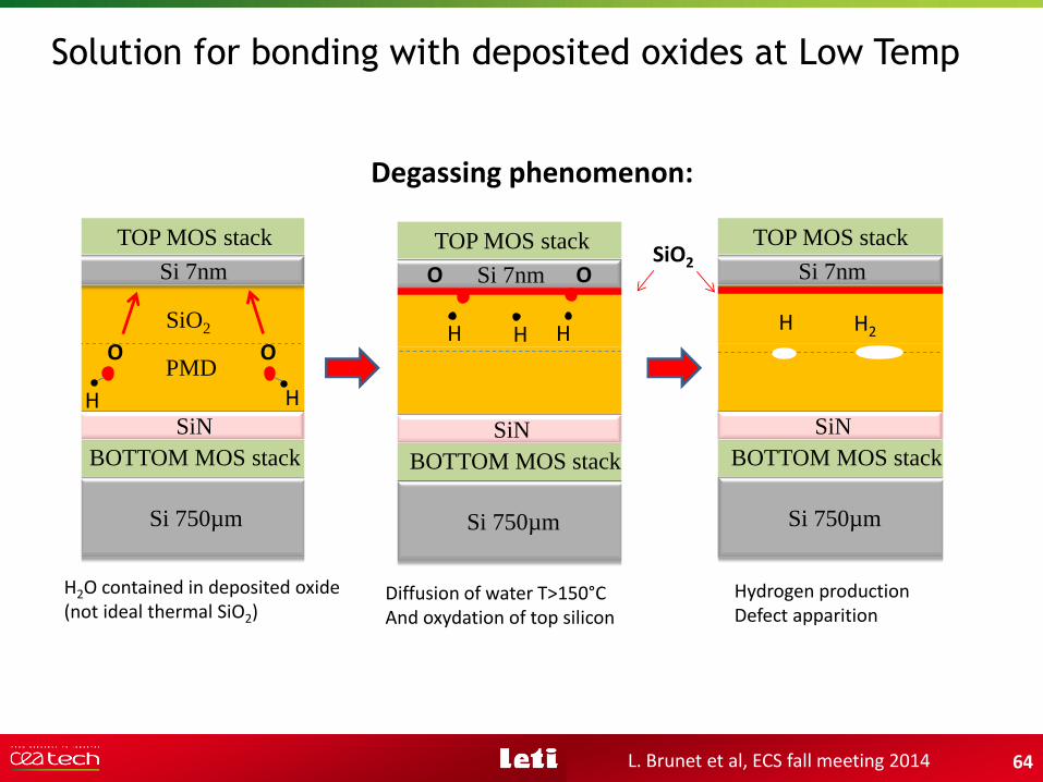
Degassing phenomenon: Solution proposed:
Solution for bonding with deposited oxides at Low Temp
H2O contained in deposited oxide(not ideal thermal SiO2)
Diffusion of water T>150°CAnd oxydation of top silicon
Hydrogen production Defect apparition
L. Brunet et al, ECS fall meeting 2014 64

Solution for bonding with deposited oxides at Low Temp
Solution proposed Si3N4 H2O barrier to avoid Si oxidation
Solution for bonding with deposited oxides at Low Temp
Si 750µm
SiN
Si 7nm
BOTTOM MOS stack
TOP MOS stack
H H
O OH20 barrier
layer
RT 200°C 2h 400°C 2h 600°C 1h
5nm SiN barrier
3nm SiN barrier
L. Brunet et al, ECS fall meeting 2014 65

3-Top FET process at low temperature
Part III - Key technological modules
(1) Bottom FDSOI FET (2) Top active layer (3) Top FET
66
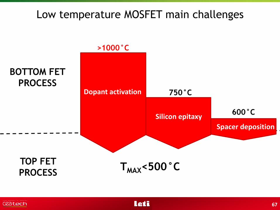
Low temperature MOSFET main challenges
TOP FET
PROCESS
>1000°C
750°C
TMAX<500°C
BOTTOM FET
PROCESSDopant activation
Silicon epitaxy600°C
Spacer deposition
67
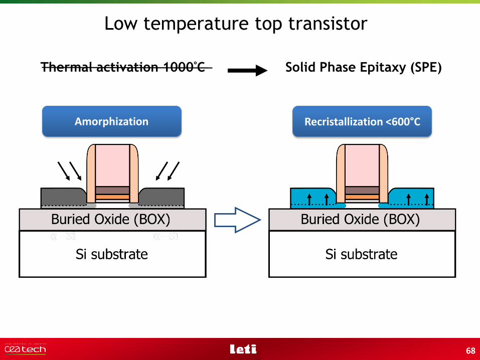
Low temperature top transistor
Solid Phase Epitaxy (SPE)Thermal activation 1000°C
Amorphization Recristallization <600°C
68
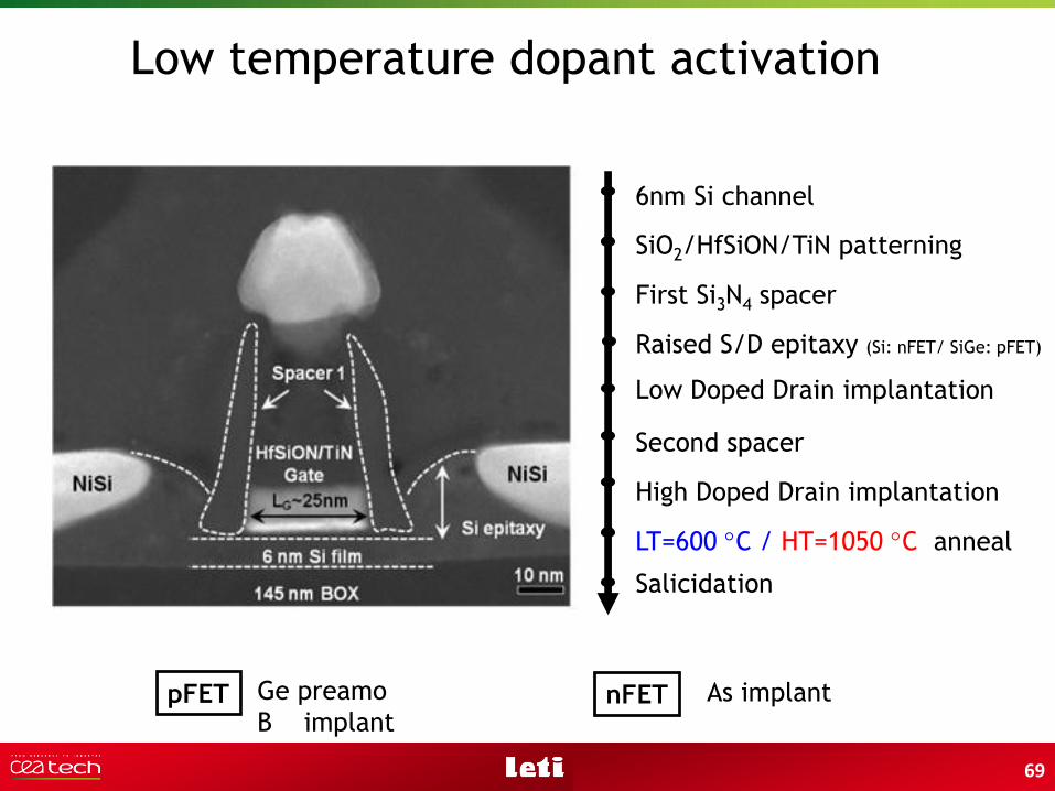
Low temperature dopant activation
6nm Si channel
SiO2/HfSiON/TiN patterning
High Doped Drain implantation
LT=600 C / HT=1050 C anneal
Raised S/D epitaxy (Si: nFET/ SiGe: pFET)
First Si3N4 spacer
Low Doped Drain implantation
Second spacer
Salicidation
Ge preamo
B implantpFET nFET As implant
69

SPER activated FDSOI devices
P. Batude et al., IEDM 2011
W=10µmVDD=1V
SPER process leads to similar performance than High T activation
High dopant activation level with 600°C process
70

Standard drawbacks observed on bulk devices:- Junction leakage increase- Deactivation
SPER FDSOI device do not present same drawbacks, why?
C. Xu et al., VLSI TSA 2012
SPER activated FDSOI devices
71
c-Si
a-Si
a/cinterface
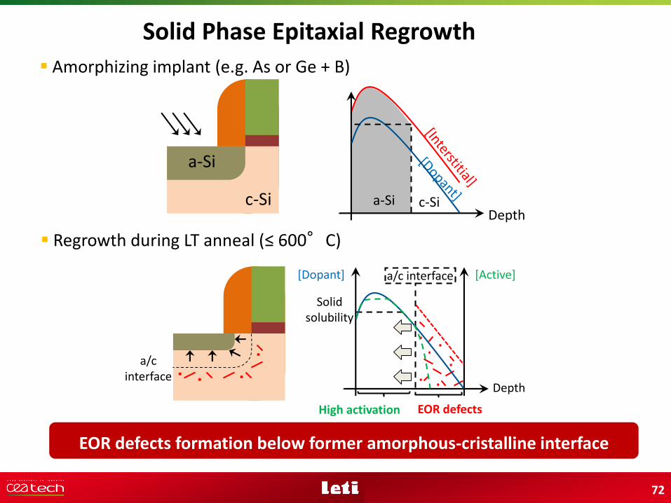
Regrowth during LT anneal (≤ 600°C)
Amorphizing implant (e.g. As or Ge + B)
Deptha-Si c-Si
Solid Phase Epitaxial Regrowth
EOR defects
[Active][Dopant]
Depth
a/c interface
Solid solubility
High activation
EOR defects formation below former amorphous-cristalline interface
72

End of Range (EOR) formation
Two phenomena during anneal:1- Defects growth through an Oswald ripening process
I4
I2
I2 I3
{311}
[In
ters
titi
al]
Depth
ΦSi i
top surface
bottomsurface
2- EOR defects dissolution via recombination at the interfaces
Dislocation loopSMICsinterstitials
BOX= New recombination
interface
73
End of Range defects in FDSOI vs BULK
Deptha-Si c-
Si
BOX
[In
ters
titi
al]
Depth
ΦSi i
BOXΦSi i
[In
ters
titi
al]
Depth
ΦSi i
top surface
(bottom surface)
Deptha-Si c-Si
1-
Du
rin
g im
pla
nta
tio
n BULK FDSOI2
-D
uri
ng
recr
ista
llisa
tio
n
top surface
(bottom surface)
Less interstitials in the c-Si film Less EOR defects
BOX= New recombination interfaceMore EOR dissolution
B. Sklenard et al.,ULIS 2012 74

Junction leakage
Tsi=25nm
Tsi=6nm
Sii sink
1,5
dec D
rain
Cu
rren
t I
D
Gate bias VG
ID,MIN
Sii sink
KMC simulations
Low T activation
For thin channel, no EOR defects at the channel entrance
No junction leakage increase
B. Sklenard et al.,ULIS 2012 75

Boron deactivation for thin SOI and BULK
Rsheet evolution with post activation anneal (spacer, BEOL..)
C. Xu et al.,IWJT 2012
Tamo= 10nm
~BULK case
~FDSOI case
Boron deactivation can be suppressed for Tseed = 5nm
76

EOR evolution with post anneals
BOX BOX
T Si= 21nm T Si= 30nm
Original situation after recristallisation anneal (original EOR reservoir is smaller in thin SOI)
During post anneal: emission of interstitial Si atoms from the EOR joining the closest sink
BOX BOX
T Si= 21nm T Si= 30nm Ф Sii,TOP
Ф Sii,TOP
Ф Sii,TOP
Ф Sii,TOP
T seed
Dopant deactivation in SOI
Scaling Tseed enable to: - reduce original EOR concentration- reduce the Sii flux crossing the highly activated region
avoiding formation of inative Boron interstitials clusters
77

Optimizing the sheet resistance
0
2
4
6
8
10
12
As+
PH
T
As+
PLT
As
LT (
Hig
h D
ose
)
As
LT (
Low
Do
se)
PLT
(H
igh
Do
se)
Rsh
eet
(a.u
.)
+86%
-18%
PLT
(Lo
wD
ose
)
Implanted Dose (1015x at/cm2)5.5 5.5 3 1 1.7 1
- HT : 1050°C spike annealing - LT : 2min 600°C SPER
Applying HT POR implant conditions leads to severe resistance degradation
Reducing implanted dose, Rsheet reduced for both As and P
L. Pasini et al., IWJT 2013
22nm SOI doped by ion implantation
78
Do
pan
t C
hem
ical
Co
nen
trat
ion
Depth
BO
X
Am
orp
ho
us
Si
Cry
stal
line
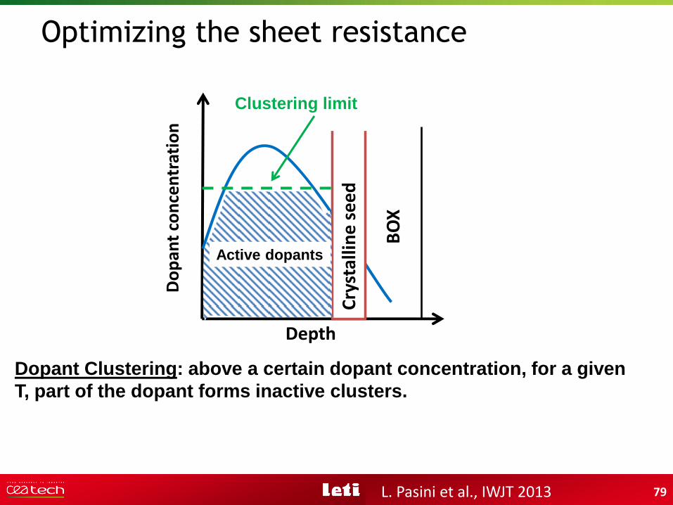
seed
Clustering limit
Dopant Clustering: above a certain dopant concentration, for a given
T, part of the dopant forms inactive clusters.
Active dopants
Optimizing the sheet resistance
L. Pasini et al., IWJT 2013
Do
pan
t co
nce
ntr
atio
n
79

x
sheet dxxµxeC
R)()(
1
Optimizing the sheet resistance
C: active concentration, µ mobility of carriers
extraction by Hall measurements
Implantation with concentration higher than clustering limit degrades either the active level and/ or carrier mobility
L. Pasini et al., IWJT 2013
PAs
Dopant concentration must not exceeds the clusterisation limit
80

• FDSOI is a key asset for low temperature junction
Indeed EOR concentration reduction enable to supress:
– Junction leakage issues
– Boron deactivation phenomenon
• Optimization of dopant concentration is needed in order to avoidimportant clusterization phenomena
• SPER activated devices have similar performance than HT spikeactivated devices
Main learnings from SPER junctions optimization
81
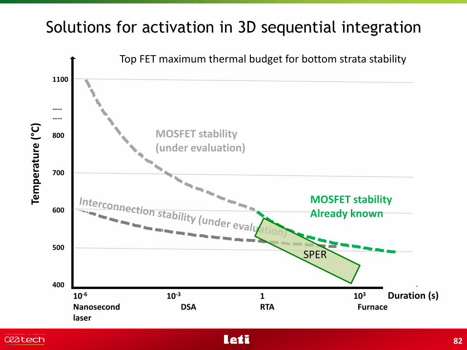
Solutions for activation in 3D sequential integrationTe
mp
era
ture
(°C
)
10-6 10-3 1 103
Nanosecond DSA RTA Furnacelaser
1100
…..…..
800
700
600
500
400
MOSFET stabilityAlready known
MOSFET stability(under evaluation)
SPER
Top FET maximum thermal budget for bottom strata stability
Duration (s)
82

Duration (s)
Tem
pe
ratu
re(°
C)
10-6 10-3 1 103
Nanosecond DSA RTA Furnacelaser
1100
…..…..
800
700
600
500
400
MOSFET stabilityAlready known
MOSFET stabilityTo evaluate
Local anneal region
Solutions for activation in 3D sequential integration
Top FET maximum thermal budget for bottom strata stability
83

Laser activation
B. Rajendran et al., TED 2007, IBM
Lg=4µm
KrF excimer laser 248nmLaser activationThermal anneal 900°C 30min
Efficiency of laser ns anneal to activatedopants proven
Protection of bottom MOSFET during laser anneal validated
BULK transistors with SiO2 poly gate stack
BULK capacitor with SiO2 aluminium gate
Promising techniques for dopant activation
Additionnal work is needed to evaluate its’ interest for 3D sequential integration: Find the laser anneal conditions to have the best gate/source-drain selectivityEvaluation of 3D pattern effect on scaled design rules and versus densityEvaluation on thin SOI devicesCompatibility with scaled ILD thicknesses
Interlayer dielectric =1µm
Some answers to be found in C. Fenouillet IEDM 2014 paper
84

Microwave annealing Equivalent activation level at 150°C lower than SPER
MWA @ 460°C
Yao-Jen Lee et al. (NDL) TED 2014
Dopant diffusion
-150°C
ClusteringphenomenaReducing SPER rate
Promising techniques for dopant activation
Additionnal work is needed to evaluate its’ interest for 3D sequential integration: Evaluation of metal interconnections (temperature depending on conductivity)
85

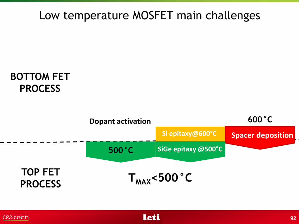
Low temperature MOSFET main challenges
TOP FET
PROCESS
>1000°C
750°C
TMAX<500°C
BOTTOM FET
PROCESSDopant activation
Silicon epitaxy600°C
Spacer deposition
86

Low temperature MOSFET main challenges
TOP FET
PROCESS
500°C
750°C
TMAX<500°C
BOTTOM FET
PROCESSDopant activation
Silicon epitaxy600°C
Spacer deposition
Dopant activation
87

Low temperature MOSFET main challenges
TOP FET
PROCESS
500°C
750°C
TMAX<500°C
BOTTOM FET
PROCESSDopant activation
Silicon epitaxy600°C
Spacer deposition
Dopant activation
88

Low temperature epitaxy
Goal: Obtain a selective epitaxy on the source & drain
Standard process: dichlorosilane and HCl flow together
dichlorosilane : deposition of Si and etch on oxide isolationHCL: etching on nitride spacer
Reasonable deposition rate cannot be obtained at temperature below 750°C
c- Si
89

Step 1- non selective growth Step 2-selective etch steps
Cyclic Deposition Etch (CDE) process
100
101
102
103
0,8 0,9 1 1,1
F(GeH4)/F(H2) = 1.33E-3No GeH4
Si0.7
Ge0.3
Si0.8
Ge0.2
Si (o
r S
iGe)
etc
h r
ate
(nm
min
.-1)
1000/T (K-1
)
F(HCl)/F(H2) = 0.167
P = 20 Torr
Ea = 44 kcal. mol.
-1
Ea = 71.5 kcal. mol.
-1
Use disilane instead of dichlorosilaneenable to increase Si deposition rate
Amorphous-Si Cristalline-Si Cristalline-Si
Low temperature epitaxy
Addition of GeH4 to HCl enableto increase the etching speed
1
10
100
1000
400 600 800 1000
SiH2Cl2SiH4Si2H6
Si g
row
th r
ate
(nm
min
.-1)
Growth temperature (°C)
650°C550°C475°C
P = 20 Torr
90

J-M. Hartmann et al., ECS journal 2014
Low temperature epitaxy
Si epitaxy @600°C SiGe 35% epitaxy @500°CJ-M. Hartmann et al., Semicond. Sci. Technol 2013
Use of new precursor for deposition such as Si3H8 and Cl2 for etching are promising for further thermal budget reduction [M. Bauer et al., Thin Solid fim 2012 ]
Work is still needed to lower the epitaxy down to 500°C
Dramatic decrease of Epitaxy thermal budget is achievable via CDE process
91
Low temperature MOSFET main challenges
TOP FET
PROCESS
500°C
TMAX<500°C
BOTTOM FET
PROCESSDopant activation
Si epitaxy@600°C
600°C
Spacer deposition
Dopant activation
SiGe epitaxy @500°C
92
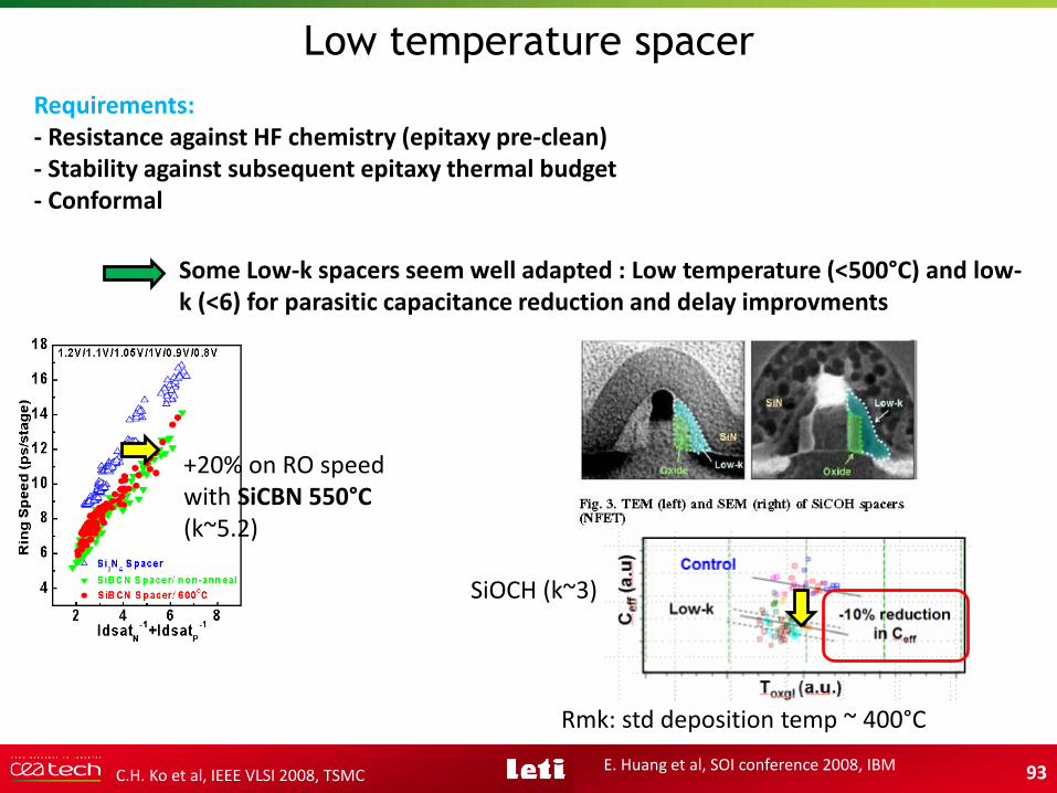
Low temperature spacer
Requirements: - Resistance against HF chemistry (epitaxy pre-clean)- Stability against subsequent epitaxy thermal budget- Conformal
Some Low-k spacers seem well adapted : Low temperature (<500°C) and low-k (<6) for parasitic capacitance reduction and delay improvments
+20% on RO speed with SiCBN 550°C(k~5.2)
C.H. Ko et al, IEEE VLSI 2008, TSMCE. Huang et al, SOI conference 2008, IBM
SiOCH (k~3)
Rmk: std deposition temp ~ 400°C
93

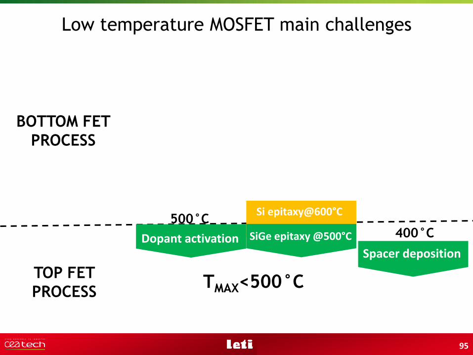
Low temperature MOSFET main challenges
TOP FET
PROCESS
500°C
600°C
TMAX<500°C
BOTTOM FET
PROCESSDopant activation
Silicon epitaxy
600°C
Spacer deposition
Dopant activation
94
Si epitaxy@600°C
SiGe epitaxy @500°C
Low temperature MOSFET main challenges
TOP FET
PROCESS
500°C
TMAX<500°C
BOTTOM FET
PROCESSDopant activation
400°C
Spacer depositionDopant activation
95
Si epitaxy@600°C
SiGe epitaxy @500°C

Some examples of 3D sequential demonstrations
S3 SRAM technology from SamsungDopant activation by high temperature spike anneal *
Top active creation by Selective Epitaxy Growth or laser liquid phase recrystallisation**
*Impossible with intermetal lines** Incompatible with bottom MOSFET stability at advanced nodes and high loss in density due to seed window area penalty
Seed
win
do
w
S-M. Jung et al., VLSI 2007, Samsung
3 level stacking! Seed window configuration
See
dw
ind
ow
SRAM butterfly curves
96

Some examples of 3D structures
Ultimate CMOS technology from AIST (InGaAsOI nFET on SGOI pFET)SBH adaptation with appropriate metallizationTop activate creation by In GaAs Direct Bonding
Full 350°C process for top FET!
Inverter Ring oscillator
T. Irisawa et al., VLSI 2014, AIST Japan 97

Transistor and Memories with vertical channel
Surrounding gate transistor from BesangTop activate creation by direct bondingDopant activation made before wafer report
Technology licensed by Hynix
S-Y. Lee, IMW 2012, Besang 98

Thin Film Transistor (Poly-Si)
Low performance compared to cristalline channel
C-C. Yang et al., IEDM 2013, NDL
High variability due to grain variable orientation and grain boundaries
« Epi-like Si FET » from NDL Dopant activation by thermal activation at unknown temperatureTop activate creation by crystallization of amorphous deposition by laser annealing
99
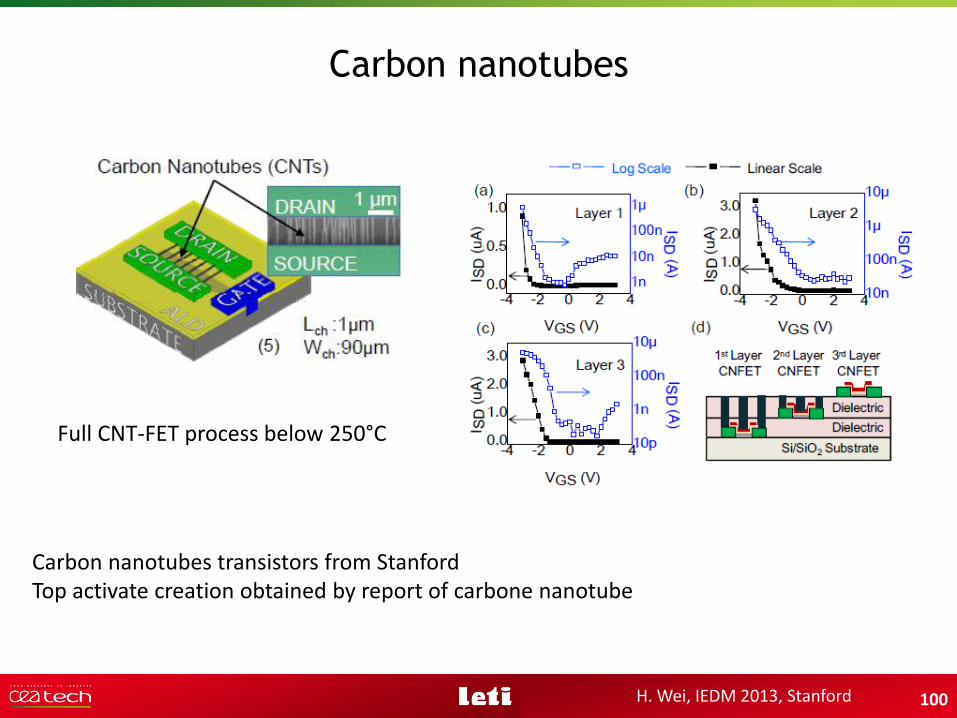
Carbon nanotubes
Full CNT-FET process below 250°C
H. Wei, IEDM 2013, Stanford
Carbon nanotubes transistors from StanfordTop activate creation obtained by report of carbone nanotube
100
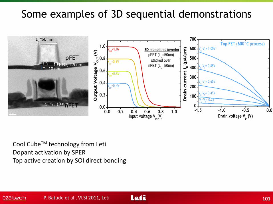
Tsi 10 nmTHFO2 2.5 nmTiN
LG~50 nm
Some examples of 3D sequential demonstrations
Cool CubeTM technology from LetiDopant activation by SPERTop active creation by SOI direct bonding
P. Batude et al., VLSI 2011, Leti
pFET
nFET0.0 0.2 0.4 0.6 0.8 1.0
0.0
0.2
0.4
0.6
0.8
1.0
VDD
=0.4V
VDD
=0.6V
VDD
=0.8V
VDD
=1.0V 3D monolithic inverter
pFET (LG=50nm)
stacked over
nFET (LG=50nm)
Outp
ut
Volt
age V
OU
T (V)
Input voltage VIN(V)
-1.5 -1.0 -0.5 0.00
100
200
300
400
500
600
700Top FET (600°C process)
VG-V
T= 0.25
VG-V
T= 0.45V
VG-V
T= 0.65V
VG-V
T= 0.85V
VG-V
T= 1.05V
Drain
current
I D (
µA/µ
m)
Drain voltage VD (V)
101
Conclusion
Roadmap driven by IC performance: 3D mono CMOS/ CMOSa path for reducing interconnection delay penaltyStacking instead of scaling: Reaching n+1 node with n node technology
Cointegration of heterogeneous functions requiring small grain partitionningHighly miniaturized CMOS image sensors/ NEM with CMOS
Roadmap driven by transistor performance :3D monolithic N/PMain advantage: easier and cheaper way to optimize the transistors’ performancea path for III-V cointegration with Ge
3D sequential integration leads to ultra high 3D contact density1x106/mm2 is demonstrated/ > 1x10⁸/mm2 is achievable with 14 nm technology
102
Conclusion
Bottom transistor preservation:
Preserved at 500°C for hours (FDSOI with NiPt salicide)
Solution might be available to increase salicide stability above to 500°C
Top transistor process:
- Direct bonding enable to achieve top active layer equivalent to bottom substrate
- Dopant activation with SPE activation leads to similar performance than the high temperature standard process
- FDSOI is a crucial asset to achieve high performance LT CMOS (EOR reduction)
-Laser (nanosecond) is a promising option for dopant activation thanks to local annealing of top layer
103

Thank you to all co-authors and colleagues that have been working on Cool CubeTM
B. Sklenard, C. Fenouillet-Beranger, L. Pasini, B. Sklenard, B.Matthieu, L. Brunet, C. Xu, B. Previtali, C. Tabone, F. Ponthenier,N. Rambal, F. Deprat, L. Tosti, L. Hortemel, M-P. Samson, O.Rozeau, O. Billoint, O. Turkyilmaz, H. Sarhan, G. Cibrario, A.Pouydebasque, F. Fournel, L. Benaissa, T. Signamarcheix, A.Seignard, C. Euvrard-Colnat, M. Rivoire, F. Nemouchi, V. Carron,F. Piegas Luce, F. Mazen, P. Besson, A. Royer, C. Agrafeil, P.Coudrain, Julien Arcamone, P-E. Gaillardon, S. Bobba, T. Ernst, C.Deguet, F. Geiger, J-E. Michallet, C. Reita, F. Clermidy, O. Faynotand M. Vinet
This work is partly funded by the ST/IBM/LETI Alliance program and by Qualcomm
Thank YOU for your attention
104


