
ORDER NO.
PIONEER ELECTRONIC CORPORATION 4-1, Meguro 1-Chome, Meguro-ku, Tokyo 153-8654, JapanPIONEER ELECTRONICS SERVICE, INC. P.O. Box 1760, Long Beach, CA 90801-1760, U.S.A.PIONEER ELECTRONIC (EUROPE) N.V. Haven 1087, Keetberglaan 1, 9120 Melsele, BelgiumPIONEER ELECTRONICS ASIACENTRE PTE. LTD. 253 Alexandra Road, #04-01, Singapore 159936 PIONEER ELECTRONIC CORPORATION 1999
FILE-TYPE COMPACT DISC PLAYER
RRV2105
T–ZZR FEB. 1999 Printed in Japan
PD-F1007THIS MANUAL IS APPLICABLE TO THE FOLLOWING MODEL(S) AND TYPE(S).
TypeModel
PD-F1007Power Requirement Remarks
MY AC220-230V
KEYBORDINPUT
1. SAFETY INFORMATION.................................... 22. EXPLODED VIEWS AND PARTS LIST ............. 33. SCHEMATIC DIAGRAM ................................... 104. PCB CONNECTION DIAGRAM ....................... 225. PCB PARTS LIST ............................................. 306. ADJUSTMENT .................................................. 347. GENERAL INFORMATION .............................. 44
7.1 PARTS ....................................................... 447.1.1 IC ....................................................... 447.1.2 DISPLAY ........................................... 47
CONTENTS7.2 DIAGNOSIS ................................................ 48
7.2.1 DISASSEMBLY ................................. 487.2.2 ERROR CCHECK DISPLAY ............. 517.2.3 EXPLANATION OF DISC DETECTION ...................................... 52
7.3 BLOCK DIAGRAM ...................................... 548. PANEL FACILITIES AND SPECIFICATIONS
....................................................... 55

PD-F1007
2
Additional Laser Caution1. Laser Interlock Mechanism
The position of the switch (VSK1011) for detectingloading state is detected by the system microprocessor,and the design prevents laser diode oscillation whenthe switch (VSK1011) is not on CLMP terminal side(CLMP signal is OFF or high level).Thus, the interlock will no longer function if the switch(VSK1011) is deliberatery set to CLMP terminal side. (lowlevel)The interlock also does not function in the test mode * .Laser diode oscillation will continue, if pin 33 ofCXA1782CQ (IC151) on the MOTHER BOARD ASSYis connected to GND, or pin 89 of IC351 (LDON) isconnected to low level (ON), or else the terminals ofQ151 are shorted to each other (fault condition).
2. When the cover is opened, close viewing of theobjective lens with the naked eye will cause exposureto a Class 1 laser beam.
This service manual is intended for qualified service technicians; it is not meant for the casualdo-it-yourselfer. Qualified technicians have the necessary test equipment and tools, and have beentrained to properly and safely repair complex products such as those covered by this manual.Improperly performed repairs can adversely affect the safety and reliability of the product and mayvoid the warranty. If you are not qualified to perform the repair of this product properly and safely, youshould not risk trying to do so and refer the repair to a qualified service technician.
1. SAFETY INFORMATION
IMPORTANTTHIS PIONEER APPARATUS CONTAINSLASER OF CLASS 1.SERVICING OPERATION OF THE APPARATUSSHOULD BE DONE BY A SPECIALLYINSTRUCTED PERSON.
REAR
PD-F1007/MY
LABEL CHECK
∗ Refer to page 35 .
LASER DIODE CHARACTERISTICS MAXIMUM OUTPUT POWER: 7 mw WAVELENGTH: 780 – 785 nm

PD-F1007
3
1
6
8
9
10
11
12
14
4
5
3
2
13
7
2. EXPLODED VIEWS AND PARTS LIST
2.1 PACKING
PACKING PARTS LIST
1 Styrol Protector F PHA13252 Styrol Protector R PHA13263 Packing Case PHG23684 Packing Sheet RHC10235 Polyethylene Bag Z21–038
(0.03 × 230 × 340)
6 Operating Instructions PRD1052(English/French/German/Italian)
7 Operating Instructions PRE1279(Dutch/Swedish/Spanish/Portuguese)
8 Remote Control Unit PWW1139(CD-PD094)
9 Battery Cover AZA7204
NSP 10 Dry Cell Batteries (R6P, AA) VEM–01311 Control Cable (L=1 m) PDE124712 Audio Cable (L=1 m) PDE1248
NSP 13 Warranty Card ARY702214 KEY Board Label PRW1527
NOTES : Parts marked by “ NSP ” are generally unavailable because they are not in our Master Spare Parts List.The mark found on some component parts indicates the importance of the safety factor of the part.Therefore, when replacing, be sure to use parts of identical designation.Screw adjacent to mark on the product are used for disassembly.
Mark No. Description Part No.

PD-F1007
4
B
A
AI
I
H
C
C
D
D
E
EF G
G
F
H
19
8
21
21
20
Refer to " 2.3 EXTERIOR (2/2)".
36
17
615
22
14(1/2)
6
12
16
20
20
20
20
10
20
20
10
23
23
7
411 (2/2)
20
20
20
11 (1/2)
2
20
20 20
20
22
22
22
13
1
14(2/2)
20205
20
Refer to " 2.5 FRONT PANEL ASSY SECTION".
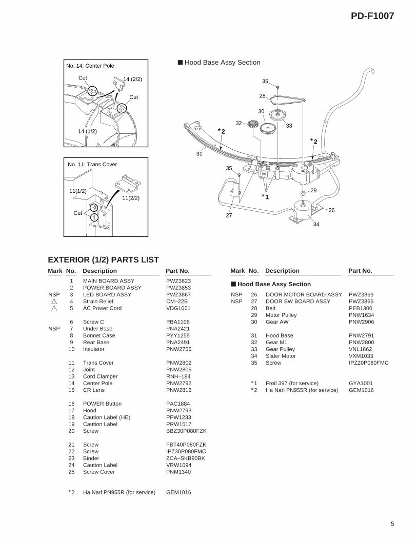
Hood Base Assy
18
24
9
25
∗2
B
2.2 EXTERIOR (1/2)
PD-F1007
5
1 MAIN BOARD ASSY PWZ38232 POWER BOARD ASSY PWZ3853
NSP 3 LED BOARD ASSY PWZ38674 Strain Relief CM–22B5 AC Power Cord VDG1061
6 Screw C PBA1106NSP 7 Under Base PNA2421
8 Bonnet Case PYY12559 Rear Base PNA2491
10 Insulator PNW2766
11 Trans Cover PNW280212 Joint PNW280513 Cord Clamper RNH–18414 Center Pole PNW279215 CR Lens PNW2816
16 POWER Button PAC188417 Hood PNW279318 Caution Label (HE) PPW123319 Caution Label PRW151720 Screw BBZ30P080FZK
21 Screw FBT40P080FZK22 Screw IPZ30P080FMC23 Binder ZCA–SKB90BK24 Caution Label VRW109425 Screw Cover PNM1340
∗2 Ha Narl PN955R (for service) GEM1016
26
34
29
35
∗1
∗2
∗2
32
30
33
28
35
31
27
EXTERIOR (1/2) PARTS LISTMark No. Description Part No.
Hood Base Assy Section
NSP 26 DOOR MOTOR BOARD ASSY PWZ3863NSP 27 DOOR SW BOARD ASSY PWZ3865
28 Belt PEB130029 Motor Pulley PNW163430 Gear AW PNW2906
31 Hood Base PNW279132 Gear M1 PNW280033 Gear Pulley VNL166234 Slider Motor VXM103335 Screw IPZ20P080FMC
∗1 Froil 397 (for service) GYA1001∗2 Ha Narl PN955R (for service) GEM1016
Mark No. Description Part No.
Hood Base Assy Section
Cut 14 (2/2)
No. 14: Center Pole
Cut
14 (1/2)
Cut
11(2/2)11(1/2)
No. 11: Trans Cover

PD-F1007
6
2.3 EXTERIOR (2/2)
A
A
B
C
B
C
52
52
53
11
52
40
3344
44
44
Refer to " 2.4 FLOAT BASEASSY SECTION".
52
52
20
15
52
28
30
37
47
32
32
32 34
32
19
32
32
32
52
5
43
2
31
41
50
39
38
652
5236
35
51
10
9
1
42
821
44
45
44
46
44
50
7
∗1
∗1
∗1
∗1
∗1
∗1
∗1
∗1
∗2

PD-F1007
7
NSP 1 SENSOR BOARD ASSY PWZ3781NSP 2 SELECT BOARD ASSY PWZ3785NSP 3 LOADING BOARD ASSY PWZ3788NSP 4 LOADING SW BOARD ASSY PWZ3790NSP 5 RADIATE BOARD ASSY PWZ3791
NSP 6 RECEIVE BOARD ASSY PWZ3792NSP 7 VOLUME BOARD ASSY PWZ3866
8 Clamp Spring ABH71079 Loading Belt AEB7029
10 Gear Pulley B ANW7062
11 Roller B ANW7075NSP 12 Arm Spring PBH1225
13 L Arm Spring PBH122614 Sheet PED102815 Clamper PNW2743
16 Gear 1 PNW281917 Gear 2 PNW282018 Gear Holder PNW282219 Slider Cam PNW282320 Clamp Support PNW2826
21 Clamp Holder PNW282722 Drive Arm PNW2829
NSP 23 Link PNW2830NSP 24 L Slider PNW2831NSP 25 L Arm PNW2832
26 Guide L PNW283327 Guide R PNW283428 Link L PNW284429 Drive Cam PNW287330 Lock Plate PNA2438
31 Motor Pulley PNW163432 Roller PNW264733 Disc Rack PNW279034 Rack Base PNW283535 ST Gear 0.6 PNW2836
36 ST Gear 1.0 PNW283737 Disc Divider PNW283838 Guide Support L PNW283939 Guide Support R PNW284040 Disc Guard PNW2841
41 Sensor Stay PNW284242 Guide Roller PNW284343 Slider Motor VXM103344 Rack Label PAM177045 S Label PAM1771
46 +1 Label PRW150747 Screw BBZ30P080FZK48 Screw BMZ26P040FZK49 Screw BPZ26P060FMC50 Screw BPZ30P100FCU
51 Screw IPZ20P080FMC52 Screw PPZ30P080FMC53 Arm Assy PXA1615
∗1 Froil 397 (for service) GYA1001∗2 Ha Narl PN955R (for service) GEM1016
EXTERIOR (2/2) PARTS LISTMark No. Description Part No.
a
a
b
bNote) Tightening Torque: 2 kg·cm
52
23
25
12
24
26
2214
29
51
9
10
4916
17
13
18
3
43
31
48
4
27
∗1
∗2 [ Apply the Guide R (No. 27) also at the same position.]
PD-F1007
8
18
20
23
12
6
11
7
1
8
9
22
21
4
16
3
2
5
10
17
14
15
24
2519
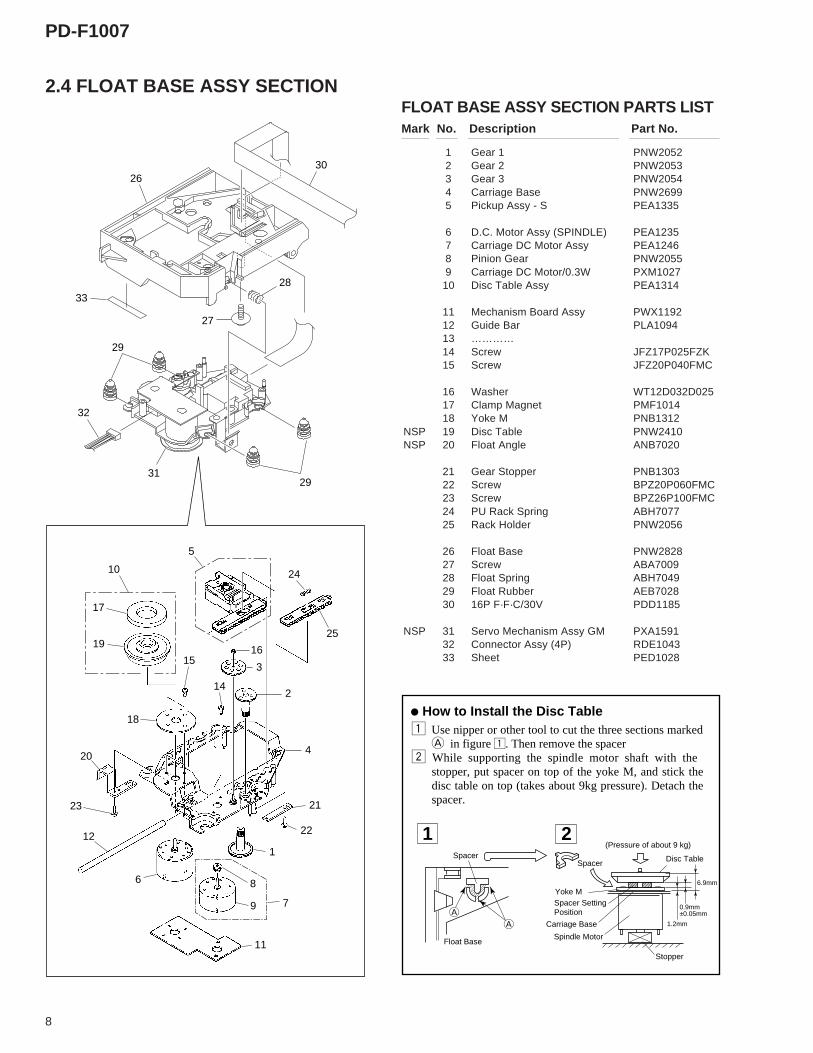
SpacerSpacer
(Pressure of about 9 kg)
Disc Table
1.2mm
6.9mm
0.9mm±0.05mm
Yoke M
Spindle Motor
Carriage Base
Stopper
Spacer SettingPosition
21
1 Use nipper or other tool to cut the three sections marked A in figure 1. Then remove the spacer
2 While supporting the spindle motor shaft with the stopper, put spacer on top of the yoke M, and stick the disc table on top (takes about 9kg pressure). Detach the spacer.
¶ How to Install the Disc Table
AA
Float Base
29
29
28
3026
33
27
31
32
1 Gear 1 PNW20522 Gear 2 PNW20533 Gear 3 PNW20544 Carriage Base PNW26995 Pickup Assy - S PEA1335
6 D.C. Motor Assy (SPINDLE) PEA12357 Carriage DC Motor Assy PEA12468 Pinion Gear PNW20559 Carriage DC Motor/0.3W PXM102710 Disc Table Assy PEA1314
11 Mechanism Board Assy PWX119212 Guide Bar PLA109413 …………14 Screw JFZ17P025FZK15 Screw JFZ20P040FMC
16 Washer WT12D032D02517 Clamp Magnet PMF101418 Yoke M PNB1312
NSP 19 Disc Table PNW2410NSP 20 Float Angle ANB7020
21 Gear Stopper PNB130322 Screw BPZ20P060FMC23 Screw BPZ26P100FMC24 PU Rack Spring ABH707725 Rack Holder PNW2056
26 Float Base PNW282827 Screw ABA700928 Float Spring ABH704929 Float Rubber AEB702830 16P F·F·C/30V PDD1185
NSP 31 Servo Mechanism Assy GM PXA159132 Connector Assy (4P) RDE104333 Sheet PED1028
FLOAT BASE ASSY SECTION PARTS LISTMark No. Description Part No.
2.4 FLOAT BASE ASSY SECTION

PD-F1007
9
811
7
12
18
2122
20
19
1
4
19
14
19
9
16
10
15
17 13
5
3
6
2
19
19
2.5 FRONT PANEL ASSY SECTION
1 DISPLAY BOARD ASSY PWZ3840NSP 2 FUNCTION BOARD ASY PWZ3847NSP 3 HEADPHONE BOARD ASSY PWZ3860
4 18P F·F·C/30V PDD11885 MODE Button PAC1880
6 PLAY Button PAC18817 Jog Dial PAC18828 ENTER Button PAC18839 Name Plate PAM1776
10 Display Window PAM1796
11 Enter Spring PBH122812 Jog Sheet PEC1042
FRONT PANEL ASSY SECTION PARTS LISTMark No. Description Part No.
13 FC Cover PNM132314 PCB Cover PNM132415 LED Lens PNW2019
16 Operation Panel PNW290917 Sensor Lens PNW280418 Rotary Knob RAC190319 Screw PPZ30P100FMC20 KEY BOARD ASSY PWZ3836
21 Screw PPZ30P050FMC22 Cord clamper RNH-184
Mark No. Description Part No.

PD-F1007
10
A
B
C
D
1 2 3 4
1 2 3 4
Note : When ordering service parts, be sure to refer to "EXPLODED VIEWS and PARTS LIST" or "PCB PARTS LIST".
Large sizeSCH diagram
Guide page
Detailed page
A-a
A-a
A-a
A-cA-b
A-b
A-b
A-d
SERVO MECHANISM ASSY(PXA1591)
MECHANISMBOARD ASSY(PWX1192)
PIC
KU
P A
SS
Y(P
EA
1335
)
A
DOOR MOTORBOARD ASSY(PWZ3863)
BDOOR SWBOARD ASSY(PWZ3865)
C
LED BOARD ASSY(PWZ3867)
D
KCN207
KCN205
KCN208
KCN202
SPINDLEMOTORASSY
PEA1235
DOOR MOTORVXM1033
CARRIADGEMOTORASSY
PEA1246
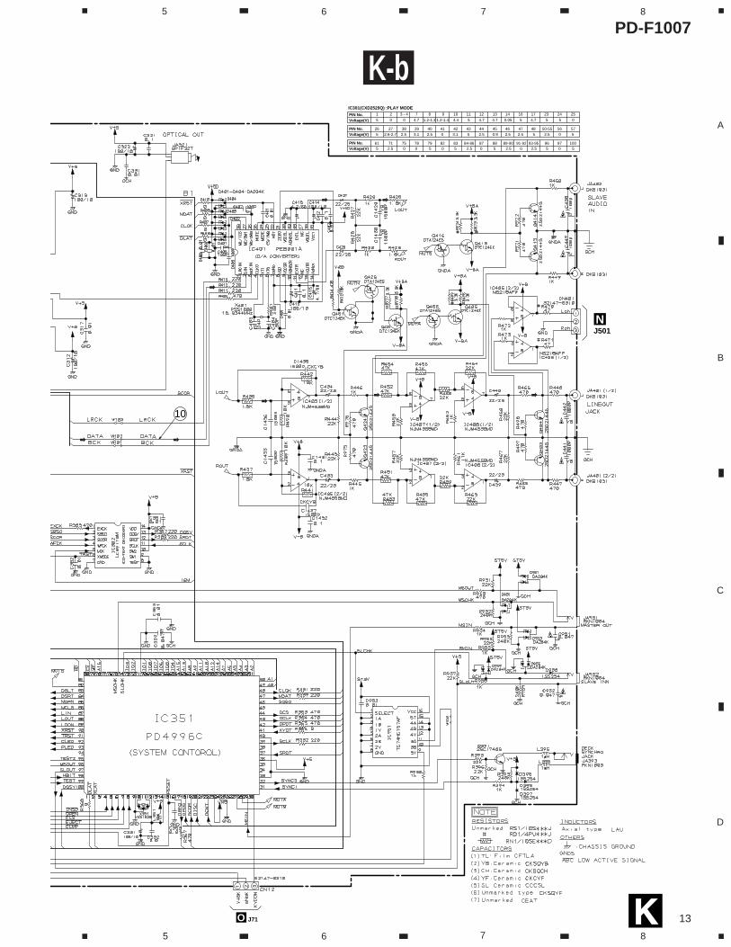
3.1 MECHANISM BOARD, DOOR MOTOR BOARD, DOOR SW BOARD, LED BOARD and PICKUP ASSEMBLIES
(T)
(T)
(F)
(F)
SIGNAL ROUTE: FOCUS SERVO LOOP: TRACKING SERVO LOOP: CARRIAGE SERVO LOOP: SPINDLE DRIVE
(S)
(C)
(T)
(F)
3. SCHEMATIC DIAGRAM

PD-F1007
11
A
B
C
D
1 2 3 4
1 2 3 4
LOADING SW ASSY(PWZ3790)
E
VOLUME BOARD ASSY(PWZ3866)
P
LOADINGBOARDASSY(PWZ3788)
F
RECIEVEBOARDASSY(PWZ3792)
H
SELECTBOARDASSY(PWZ3785)
J
RADIATEBOARDASSY(PWZ3791)
I
SENSOR BOARDASSY(PWZ3781)
G
SELECT MOTORVXM1033
LOADING MOTORVXM1033
22k
D20
PD
Y03
10E
J605
1.5k
100k
100k
150
J604D20PDY0315E
VR601
CN605 CN60452147–0310 ×2
REAF SWVSK1011
KCN203
KCN204
3.2 LOADING SW, LOADING BOARD, SENSOR BOARD, RECIEVE BOARD, RADIATE BOARD and SELECT BOARD ASSEMBLIES

PD-F1007
12
A
B
C
D
1 2 3 4
1 2 3 4
K-a
MAINBOARDASSY(PWZ3823)
K
BJ631
JJ601
FJ651
A
CN
610
to P
ICU
P A
SS
Y
DJ1601
O J11 L J701
1.8V
1.8V
-0.7V
1.6V
1.6V
0V
1.6V
1.6V
0V
1.7V
1.7V
0.2V
0V
0V
0V
0V
0V
0V
CAUTION : FOR CONTINUED PROTECTION AGAINST RISK OF FIRE, REPLACE ONLY WITH SAME TYPE NO. ICP-N10, MFD BY ROHM CO., FOR IC35 AND IC36.
2SD2144S
SIGNAL ROUTE: AUDIO SIGNAL : EFM SIGNAL: FOCUS SERVO LOOP: TRACKING SERVO LOOP: CARRIAGE SERVO LOOP: SPINDLE DRIVE: LOADING DRIVE: DOOR DRIVE: SELECT DRIVE
(S)
(C)
(T)
(F)
(D)
(SEL)
(L)
(S)
(S)
(S)
(F)
(F)
(F)
(F)
(F)
(F)
(T)
(T)
(T)
(T)
(C)
(L)
(L)
(L)
(SEL)
(SEL)
(SE
L)
(D)
(D)
(D)
(F)
(T)
(C)
(F)
(F)
(F)
(F)
(T)
(T)
7
5
6
8
2 2343
33
53
18
19 16
23
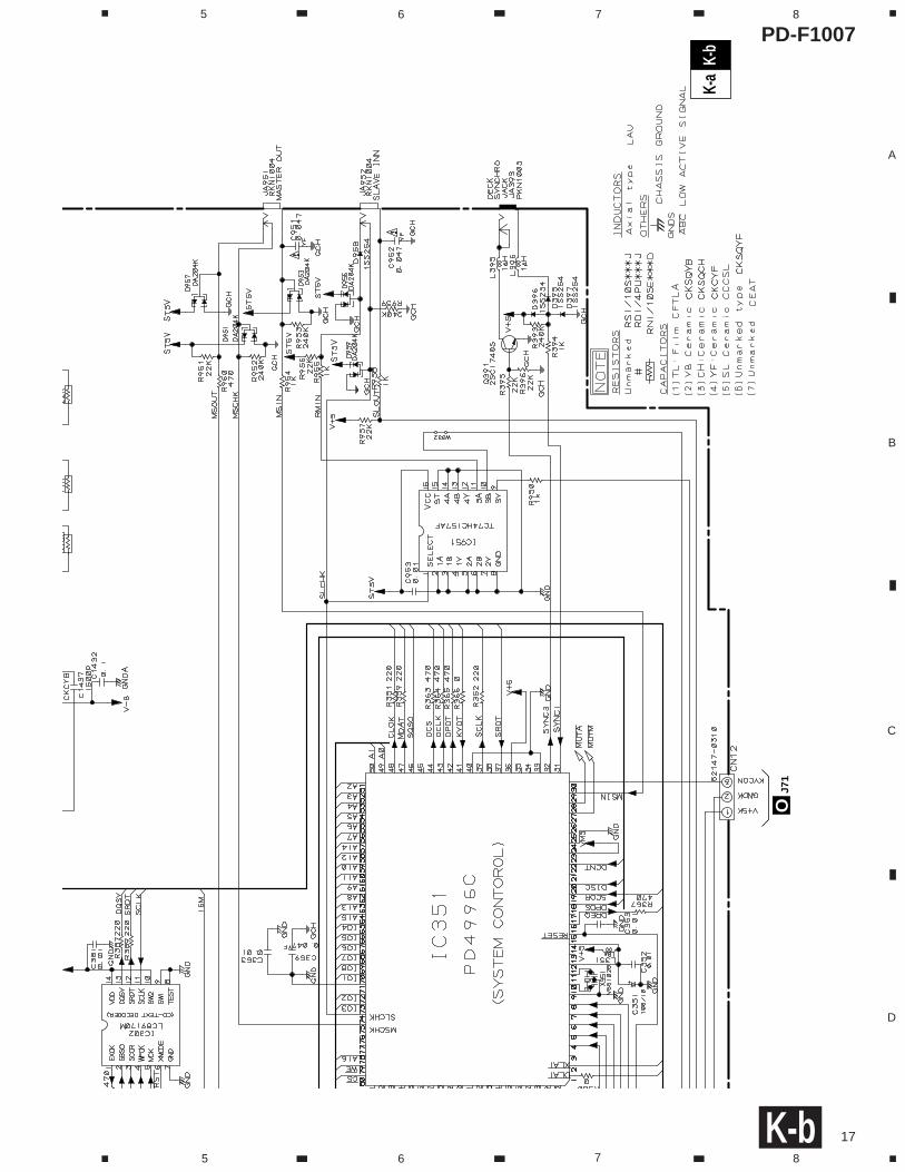
3.3 MAIN BOARD ASSY
PD-F1007
13
A
B
C
D
5 6 7 8
5 6 7 8
K-b
O J71
NJ501
IC301(CXD2529Q) :PLAY MODE
PIN No.Voltage(V)
PIN No.Voltage(V)
PIN No.Voltage(V)
1 2 3 - 4 7 8 9 10 11 12 13 14 16 17 23 24 25
26 27 38 39 40 41 42 43 44 45 46 47 48 50-55 56 57
61 71 75 78 79 82 83 87 88 89-9084-86 91-92 93-95 9796 100
5
5
5
5 5
5 5 5 50 00
0 0 5 0 5 0 5 0 5 0 5
0 50
4.7
2.5
2.5 2.5 2.5 2.5
3.1 3.12.5 2.5 0.9 2.5 2.5 2.5
4.4 4.7 4.7 4.71.2-1.41.2-1.3
2.6-2.7
0.05
10

PD-F1007
14
A
B
C
D
1 2 3 4
1 2 3 4
MA
INB
OA
RD
AS
SY
(PW
Z38
23)
K
FJ6
51
ACN610 to PICUP ASSY
1.8V
1.8V
-0.7
V
1.6V
1.6V
0V
1.6V
1.6V
0V
1.7V
1.7V
0.2V
0V
0V
0V
CA
UT
ION
: F
OR
CO
NT
INU
ED
PR
OT
EC
TIO
N A
GA
INS
T R
ISK
OF
FIR
E,
RE
PLA
CE
ON
LY W
ITH
SA
ME
TY
PE
NO
. IC
P-N
10, M
FD
BY
R
OH
M C
O.,
FO
R IC
35 A
ND
IC36
.
(S)
(S)
(S)
(F)
(F)
(F)
(F)
(F)
(F)
(T)
(T)
(T)
(T)
(C)
(L)
(L)
(L)
(SE
L)
(SE
L)
(SEL)
(F)
(F)
(F)
(F)
(F)
(T)
(T)
7
5
6 8
223
43
33
53 18 1916
K-b
K-a
K-a

PD-F1007
15
A
B
C
D
5 6 7 8
5 6 7 8
BJ6
31
JJ6
01FJ6
51
DJ1
601
OJ1
1L
J701
0V
0V
0V
2SD
2144
S
SIG
NA
L R
OU
TE
: AU
DIO
SIG
NA
L : E
FM
SIG
NA
L: F
OC
US
SE
RV
O L
OO
P: T
RA
CK
ING
SE
RV
O L
OO
P: C
AR
RIA
GE
SE
RV
O L
OO
P: S
PIN
DLE
DR
IVE
: LO
AD
ING
DR
IVE
: DO
OR
DR
IVE
: SE
LEC
T D
RIV
E
)))) ) L))
(SE
L)
(SE
L)
(SEL)
(D)
(D)
(D)
(F)
(T)
(C)
23
K-b
K-a
K-a

PD-F1007
16
A
B
C
D
1 2 3 4
1 2 3 4
N J501
IC30
1(C
XD
2529
Q)
:PL
AY
MO
DE
PIN
No
.V
olt
age(
V)
PIN
No
.V
olt
age(
V)
PIN
No
.V
olt
age(
V)
12
3 -
47
89
1011
1213
1416
1723
2425
2627
3839
4041
4243
4445
4647
4850
-55
5657
6171
7578
7982
8387
8889
-90
84-8
691
-92
93-9
5 97
9610
0
5 5 5
55
55
55
00
0 00
50
50
50
50
5
05
0
4.7
2.5
2.5
2.5
2.5
2.5
3.1
3.1
2.5
2.5
0.9
2.5
2.5
2.5
4.4
4.7
4.7
4.7
1.2-
1.4
1.2-
1.3
2.6-
2.7
0.05
10
K-b
K-a
K-b
PD-F1007
17
A
B
C
D
5 6 7 8
5 6 7 8
OJ7
1
K-b
K-a
K-b
PD-F1007
18
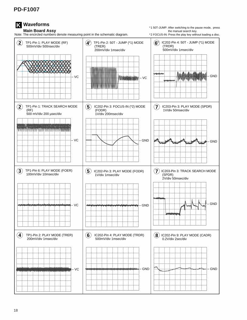
Note: The encircled numbers denote measuring point in the schematic diagram.
∗1 50T-JUMP: After switching to the pause mode, press the manual search key.∗2 FOCUS-IN: Press the play key without loading a disc.
TP1-Pin 1: PLAY MODE (RF) 500mV/div 500nsec/div
IC202-Pin 9: PLAY MODE (CADR) 0.2V/div 2sec/div
2
2 5
5 7
7
864
3
6'4'
TP1-Pin 1: TRACK SEARCH MODE (RF) 500 mV/div 200 µsec/div
TP1-Pin 6: PLAY MODE (FOER) 100mV/div 10msec/div
TP1-Pin 2: PLAY MODE (TRER) 200mV/div 1msec/div
TP1-Pin 2: 50T - JUMP (*1) MODE (TRER) 200mV/div 1msec/div
IC202-Pin 3: FOCUS-IN (*2) MODE (FODR) 1V/div 200msec/div
IC202-Pin 3: PLAY MODE (FODR) 1V/div 1msec/div
IC202-Pin 4: PLAY MODE (TRDR) 500mV/div 1msec/div
IC202-Pin 4: 50T - JUMP (*1) MODE (TRDR) 500mV/div 1msec/div
IC203-Pin 3: PLAY MODE (SPDR) 1V/div 50msec/div
IC203-Pin 3: TRACK SEARCH MODE (SPDR) 2V/div 50msec/div
– VC – VC
– VC
– VC
– VC – GND
– GND
– GND
– GND
– GND
– GND
– GND
Waveforms Main Board AssyK

PD-F1007
19
IC301-Pin 38 : PLAY MODE (PCO) 2V/div 10 µsec/div
53
33
19
23
10
18
168 IC202-Pin 9: TRACK SEARCH MODE (CADR) 2V/div 200msec/div
IC301-Pin 86 : PLAY MODE (1kHz) (LOUT 1) 1V/div 200msec/div
IC301-Pin 54 : PLAY MODE (1kHz) (BCK) 2V/div 500nsec/div
IC301-Pin 50 : PLAY MODE (1kHz) (LRCK) 2V/div 10 µsec/div
IC301-Pin 52 : PLAY MODE (1kHz) (PCMD) 2V/div 500nsec/div
TRACK SEARCH MODE Upper : TP1-Pin 1 (RF) 1V/div Lower : IC151-Pin 23 (C.OUT) 2V/div 50 µsec/div
IC301-Pin 27 : PLAY MODE (MDP) 2V/div 2 µsec/div
– GND
– GND
– GND
– GND
– GND
– GND
– GND– GND
– GND

PD-F1007
20
A
B
C
D
1 2 3 4
1 2 3 4
DISPLAY BOARD ASSY(PWZ3840)
LK CN351
DISPLAY BOARD ASSYS701 : MODES702 : CLEARS703 : PROGRAMS704 : RANDOMS705 : TIME/CHARAS706 : POWERS707 : SINGLE LOADER ACCESSS708 : SINGLE LOADER PLAY
3.4 DISPLAY BOARD, FUNCTION BOARD, HEADPHONE BOARD and POWER BOARD ASSEMBLIES
Q
J801

PD-F1007
21
A
B
C
D
1 2 3 4
1 2 3 4
HEADPHONEBOARD ASSY(PWZ3860)
N
FUNCTION BOARD ASSY(PWZ3847)
M
POWER BOARD ASSY(PWZ3853)
O
KCN11
KCN12
KCN401
To
AC
PO
WE
R C
OR
D
NE
UT
RA
L
LIVE
FUNCTION BOARD ASSYS751–S760 : DIRECT CUSTOM (1–10)S761 : Track/Manual search (reverse direction)S762 : Track/Manual search (forward direction)S763 : TITLE/DISPLAYS764 : TITLE/SEARCHS765 : OPEN/CLOSES766 : UNLOADS767 : Play/PauseS768 : StopS769 : ENTERS770 : TITLE/INPUTS771 : Jog dial
L
KEY BOARD ASSY(PWZ3836)
Q
CN
702
Q

PD-F1007
22
A
B
C
D
1 2 3 4
1 2 3 4
NOTE FOR PCB DIAGRAMS:1. Part numbers in PCB diagrams match those in the schematic diagrams.2. A comparison between the main parts of PCB and schematic diagrams is shown below.
3. The parts mounted on this PCB include all necessary parts for several destination. For further information for respective destinations, be sure to check with the schematic diagram.
4. Viewpoint of PCB diagrams
Symbol in PCBDiagrams
Symbol in SchematicDiagrams Part Name
Transistor
Transistorwith resistor
Field effecttransistor
Resistor array
3-terminalregulator
B C E
B C E
B C E
D G S
B C E
B C E B C E
D G S D G S
CapacitorConnector
P.C.Board Chip Part
SIDE A
SIDE B
MECHANISM BOARD ASSYA
DOOR MOTOR BOARD ASSYB
DOOR SW BOARD ASSYC
LED BOARD ASSYD
CARRIAGEMOTOR
MSPINDLEMOTOR
M
INSIDE
K CN207
K CN205
K CN208
(PNP1239-C)
(PNP1451-D)
(PNP1451-D )
(PNP1451-D)
4.1 MECHANISM BOARD, DOOR MOTOR BOARD, DOOR SW BOARD and LED BOARD ASSEMBLIES
SIDE A
4. PCB CONNECTION DIAGRAM

PD-F1007
23
A
B
C
D
1 2 3 4
1 2 3 4
KCN203
KCN204
LOADING BOARD ASSYF
RADIATE BOARD ASSYI
SENSOR BOARD ASSYG
SELECT BOARD ASSYJ
RECIEVEBOARD ASSYH
VOLUMEBOARD ASSYP
LOADING SW ASSYE
(PNP1452-B)(PNP1452-B)
(PNP1452-B)
(PNP1452-B)
(PNP1452-B)
(PNP1452-B)
(PNP1451-D)
4.2 LOADING SW, LOADING BOARD, SENSOR BOARD, RECIEVE BOARD, RADIATE BOARD, SELECT BOARD and VOLUME BOARD ASSEMBLIES
SIDE A

PD-F1007
24
A
B
C
D
1 2 3 4
1 2 3 4
IC25 Q351 IC36IC35IC23
IC32IC31
IC201IC202
IC203 IC34 Q391
VR152 VR153VR156VR151VR155VR154
Q151IC21
OJ11
LCN701
J J601
A CN610
To PICKUP ASSY
MAIN BOARD ASSYK4.3 MAIN BOARD ASSY, HEADHONE and KEY BOARD ASSY
SIDE A

PD-F1007
25
A
B
C
D
5 6 7 8
5 6 7 8
VR153
Q151 Q414 Q413 Q424 Q403 Q423Q404
D J1601 B J631
F J651
L
CN702
HEADPHONE BOARD ASSYN
KEY BOARD ASSYQ
(PNP1450-A)
(PNP1451-D)
SIDE A
Q
PD-F1007
26
A
B
C
D
1 2 3 4
1 2 3 4
MAIN BOARD ASSYK
KEY BOARD ASSYQ
Q451 IC341IC401
Q425 Q405 Q415 IC301 Q152 ICQ426
IC405IC407IC408IC406
Q471Q470
(PNP1450-A)
SIDE B
SIDE B
Q

PD-F1007
27
A
B
C
D
5 6 7 8
5 6 7 8
IC301 Q152 IC331 IC151 Q406 Q416 Q362Q381
IC351IC352
Q363Q382
SIDE B

PD-F1007
28
A
B
C
D
1 2 3 4
1 2 3 4
DISPLAY BOARD ASSYL
FUNCTION BOARD ASSYM
KCN351
QJ801
(PNP1451-D)
(PNP1451-D)
4.4 DISPLAY BOARD and FUNCTION BOARD ASSEMBLIES
SIDE A
PD-F1007
29
A
B
C
D
1 2 3 4
1 2 3 4
KCN11
POWER BOARD ASSYO
To
AC
PO
WE
R C
OR
D
NEUTRAL
LIVE
(PNP1451-D)
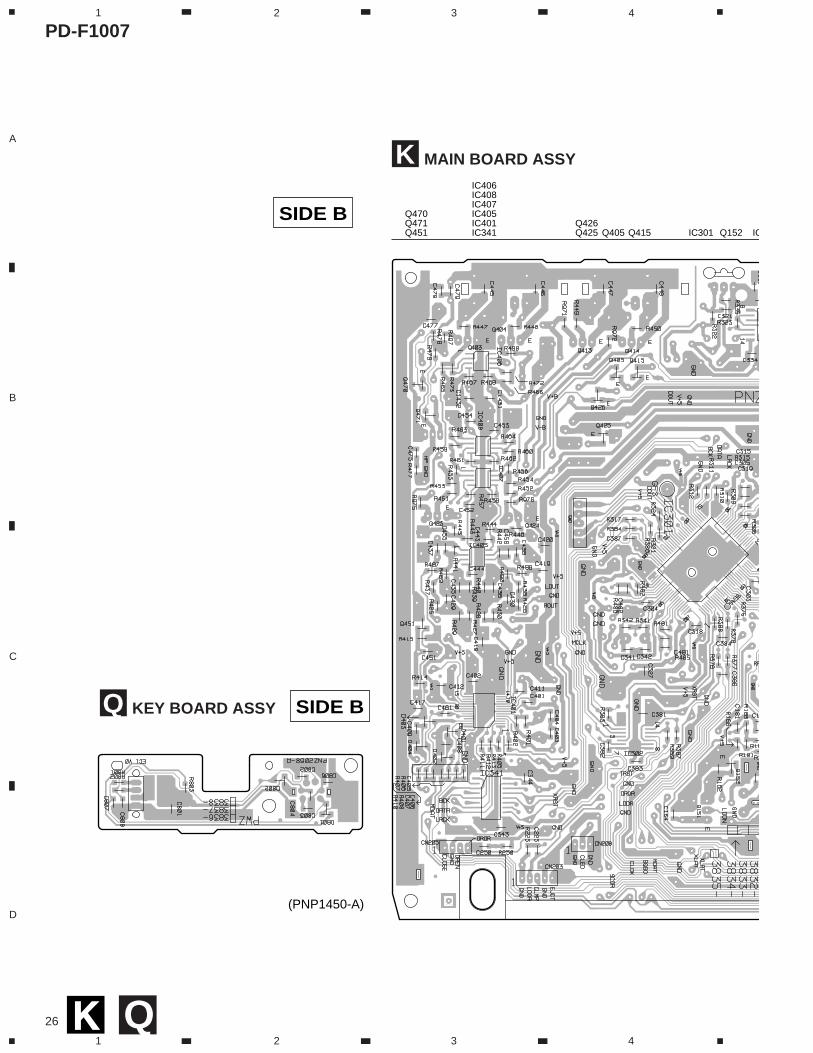
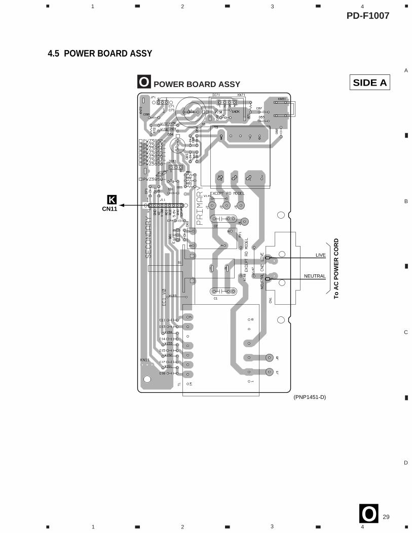
4.5 POWER BOARD ASSY
SIDE A

PD-F1007
30
LIST OF PCB ASSEMBLIESNSP MOTHER BOARD ASSY PWM2253
MAIN BOARD ASSY PWZ3823 KEY BOARD ASSY PWZ3836
NSP MECHANISM BOARD ASSY PWX1572NSP SENSOR BOARD ASSY PWZ3781NSP SELECT BOARD ASSY PWZ3785NSP LOADING BOARD ASSY PWZ3788NSP LOADING SW BOARD ASSY PWZ3790NSP RADIATE BOARD ASSY PWZ3791NSP RECIEVE BOARD ASSY PWZ3792
NSP SUB BOARD ASSY PWX1577 DISPLAY BOARD ASSY PWZ3840
NSP FUNCTION BOARD ASSY PWZ3847 POWER BOARD ASSY PWZ3853
NSP HEADPHONE BOARD ASSY PWZ3860NSP DOOR MOTOR BOARD ASSY PWZ3863NSP DOOR SW BOARD ASSY PWZ3865NSP VOLUME BOARD ASSY PWZ3866NSP LED BOARD ASSY PWZ3867
NSP SERVO MECHANISM ASSY GM PXA1591 MECHANISM BOARD ASSY PWX1192
MECHANISM BOARD ASSYSWITCHES AND RELAYS
S610 DSG1016
OTHERSCN610 MT CONNECTOR 173979-4
SENSOR BOARD ASSYSEMICONDUCTORS
Q604 2SC1740SQ601, Q602 DTC124ESD601, D602 GP1S58V
RESISTORSAll Resistors RD1/4PU J
Mark No. Description Part No. Mark No. Description Part No.
5. PCB PARTS LISTParts marked by "NSP" are generally unavailable because they are not in our Master Spare Parts List.The mark found on some component parts indicates the importance of the safety factor of the part.Therefore, when replacing, be sure to use parts of identical designation.When ordering resistors, first convert resistance values into code form as shown in the following examples.Ex.1 When there are 2 effective digits (any digit apart from 0), such as 560 ohm and 47k ohm (tolerance is shown by J=5%, and K=10%).
Ex.2 When there are 3 effective digits (such as in high precision metal film resistors).
5 6 14 7 3
R 5 01 R 0
5 6 2 1
NOTES:
56047k 0.51
RD1/4PU JRD1/4PU JRN2H KRS1P K
56 x 101
47 x 103 R501R0
561473
5.62k RN1/4PC F562 x 101 5621
OTHERS CABLE HOLDER 51048-0300 CABLE HOLDER 51048-0700J603 3P JUMPER WIRE D20PDD0310EJ602 7P JUMPER WIRE D20PDD0725EJ605 3P JUMPER WIRE D20PDY0310E
SELECT BOARD ASSYOTHERS
CABLE HOLDER 51048-0700 CABLE HOLDER 51048-0900J601 9P JUMPER WIRE D20PDY0930G
LOARDING BOARD ASSYOTHERS
CABLE HOLDER 51048-0300 CABLE HOLDER 51048-0500J652 3P JUMPER WIRE D20PDD0310EJ651 5P JUMPER WIRE D20PDY0530E
LOARDING SW BOARD ASSYOTHERS
CABLE HOLDER 51048-0300 REAF SWITCH VSK1011
RADIATE BOARD ASSYSEMICONDUCTORS
D611 GL381J
OTHERS CABLE HOLDER 51048-0300 L.E.D. HOLDER RNK1795

PD-F1007
31
Mark No. Description Part No. Mark No. Description Part No.
RECIEVE BOARD ASSYSEMICONDUCTORS
Q621 PT381FBC
OTHERS CABLE HOLDER 51048-0300J604 3P JUMPER WIRE D20PDY0315E
MAIN BOARD ASSYSEMICONDUCTORS
IC151 CXA1782CQIC301 CXD2529QIC35, IC36 (0.4A/50V) ICP-N10IC203 LA6517IC201, IC202 LA6520
IC302 LC89170MIC406 M5218AFPIC352 M5M51008BFP-70LLIC405, IC407, IC408 NJM4558MDIC23 NJM79M05FA
IC351 PD4996CIC21 PQ05RR12IC401 PE8001AIC25 S-806EIC951 TC74HC157AF
Q151 2SA854SQ391 2SC1740SQ362, Q381 2SC2412KQ351, Q403, Q404, Q413, Q414 2SD2144SQ423, Q424 2SD2144S
Q152, Q363, Q382, Q406, Q416 DTA124EKQ426 DTA124EKQ405, Q415, Q425, Q451 DTC124EKD351, D352, D395– D397, D958 1SS133D401– D404, D951, D953, D956 DA204K
D957, D959 DA204KD54 MTZJ24BD11– D14, D52 S5688GD218 UDZS6.2B
COILS AND FILTERSL351 LAU100JL395, L396 LAU1R0J
CAPACITORSC449, C450 CCCSL101J50C181 CCSQCH100D50C361, C386, C405– C407 CCSQCH101J50C315 CCSQCH221J50C403 CCSQCH240J50
C404 CCSQCH300J50C171, C175, C27, C29 CEAT101M10C301, C302, C311– C314, C316 CEAT101M10C322, C351, C365, C413, C414 CEAT101M10C51 CEAT101M35
C52 CEAT101M50C427, C428, C433, C434, C439, C440 CEAT220M25C131–C133, C211, C212 CEAT330M16C169, C170, C415, C416 CEAT4R7M50C22 CEATR22M50
C309 CEATR47M50C954 CFTLA104J50C441, C442 CKCYB102K50C1429, C1430, C1435– C1438 CKCYB152K50C317 CKCYF103Z50
C359, C951, C952 CKCYF473Z50C163 CKSQYB102K50C156, C161, C164, C168, C218 CKSQYB103K50C153– C155, C158, C230, C250 CKSQYB104K25C176, C306 CKSQYB152K50
C305 CKSQYB222K50C162 CKSQYB332K50C160 CKSQYB333K25C167 CKSQYB472K50C152, C307 CKSQYB473K25
C151 CKSQYB682K50C157 CKSQYB823K25C159, C185, C191, C205, C210 CKSQYF103Z50C215, C219, C303, C308, C318 CKSQYF103Z50C331, C352, C353 CKSQYF103Z50
C362, C363, C381, C382, C401 CKSQYF103Z50C402, C408, C409, C461, C953 CKSQYF103Z50C321, C411, C412, C1431,C1432 CKSQYF104Z50C354 (0.1F/5.5V) PCH1133C25, C26 (4700µF/16V) PCH1135
RESISTORSR56– R59 RD1/4PU241JR52– R54 RD1/4PU272JR496, R499, R973, R974 RD1/4PU332JR977, R978 RD1/4PU332JR163, R164, R470, R471 RD1/4PU470J
R441, R442, R489, R490 RN1/10SE1002DR437, R438 RN1/10SE1801DR459, R460, R463, R464 RN1/10SE2202DR451– R456 RN1/10SE4702DVR153, VR155 (10kΩ) VCP1156
VR151, VR152, VR154 (22kΩ) VCP1158VR156 (220kΩ) VCP1164Other Resistors RS1/10S J
OTHERSCN207 MT 4P CONNECTOR 173981-4CN12 3P JUMPER CONNECTOR 52147-0310CN208, CN401 3P JUMPER CONNECTOR 52147-0310CN205 4P JUMPER CONNECTOR 52147-0410CN203 5P JUMPER CONNECTOR 52147-0510CN11, CN204 9P JUMPER CONNECTOR 52147-0910

PD-F1007
32
Mark No. Description Part No. Mark No. Description Part No.
JA401, JA402 2P JACK DKB1031JA321 OPTICAL LINK OUT GP1F32TCN351 CONNECTOR HLEM18S-1JA393 JACK PKN1005X401 XTAL. RES. (16.9344MHz) PSS1008
JA951, JA952 JACK REMOTE RKN1004CN201 CONNECTOR 6P RKP-533CN202 CONNECTOR SLW16S-1C7 PCB BINDER VEF1040 SCREW PLATE VNE1948
X351 CERAMIC RES.(4.19MHz) VSS1028
DISPLAY BOARD ASSYSEMICONDUCTORS
IC701 PD4997AQ702– Q705 DTC124ESD701– D705 1SS254D751 SLR-343VC
SWITCHES AND RELAYSS701– S705, S707, S708 VSG1009
CAPACITORSC706 CEAL100M50C701, C702 CEAL101M6R3C710, C711 CEAT100M50C703 CKCYF103Z50C704, C705 CKPUYF103Z25
C707, C708 CKPUYF104Z50
RESISTORSAll Resistors RD1/4PU J
OTHERS CABLE HOLDER(14P) 51048-1400 CABLE HOLDER(13P) 51048-1300 CABLE HOLDER(12P) 51063-1205J701 JUMPER WIRE D15A12-400-2651 REMOTE RECEIVER UNIT GP1U28X
CN701 CONNECTOR 18P HLEM18R-1CN702 CONNECTOR 4P 52151-0410V701 FL INDICATOR TUBE PEL1096X701 CERAMIC RES.(4.19MHz) VSS1028J702 EARTH LEAD WIRE DE010WE0
FUNCTION BOARD ASSYSWITCHES AND RELAYS
S771 PSX1002S751– S770 VSG1009
CAPACITORSC751, C752 CKPUYF103Z25
OTHERS CABLE HOLDER(12P) 51063-1205
POWER BOARD ASSYSEMICONDUCTORS
IC61 NJM78M56FAIC71 PQ05RA1Q61 DTC124ESD63 1SS133D61, D71, D72 S5688G
SWITCHES AND RELAYSS1 RSA1001RY1 PSR1003
CAPACITORSC1, C2 (10000pF/250V) ACG7020C74 CCCSL101J50C65, C72 CEAT101M10C71 CEAT332M16C64 CEAT471M25
C11, C13– C17, C61– C63 CKCYF103Z50
RESISTORSAll Resistors RD1/4PU J
OTHERS CABLE HOLDER 51048-0900T2 POWER TRANSFORMER ATT1193J11 JUMPER WIRE D20PDY0925GJ71 JUMPER WIRE D20PDY0315ET1 POWER TRANSFOMER PTT1349
CN2 AC CORD SOCKET RKP1751 3P CABLE HOLDER 51048-0300 SCREW PLATE VNE1948KN11 EARTH METAL FITTING VNF1084 CAPACITOR COVER REC-150
HEAT SINK RNE1011
HEADRHONE BOARD ASSYCOILS AND FILTERS
L501, L504, L505 LAU1R0J
CAPACITORSC501, C502 CKCYF103Z50C503 CGCYX473K25
RESISTORSVR501 (0.5kΩ– B) PCS1003

PD-F1007
33
Mark No. Description Part No.
OTHERS 3P CABLE HOLDER 51048-0300J501 JUMPER WIRE D20PDY0355GJA501 JACK RKN1002
DOOR MOTOR BOARD ASSYOTHERS
3P CABLE HOLDER 51048-0300 4P CABLE HOLDER 51048-0400J631 JUMPER WIRE D20PDY0445G
DOOR SW BOARD ASSYOTHERS
3P CABLE HOLDER 51048-0300J632 3P JUMPER WIRE D20PDD0315E REAF SWITCH VSK1011
VOLUME BOARD ASSYRESISTORS
VR601 (22kΩ) VCP1158
OTHERSCN604, CN605 3P JUMPER CONNECTOR 52147-0310KN601 JUMPER TERMINAL PKX1001
LED BOARD ASSYSEMICONDUCTORS
D1601– D1603 SLR-343YC
RESISTORSAll Resistors RD1/4PU J
OTHERS 3P CABLE HOLDER 51048-0300J1601 JUMPER WIRE D20PDY0325E
SEMICONDUCTORSD801, D802 DA204K
CAPACITORSC805 CEAL101M6R3C801– C804, C806 CKSQYF104Z50
RESISTORSR801– R803 RS1/10S0R0J
OTHERSJ801 4P JUMPER WIRE D20PWY0455E
NSP J802 LEAD WIRE UNIT PDF1012JA801 MIN DIN 6P SOCKET RKN1038
KEY BOARD ASSYQ

PD-F1007
34
6. ADJUSTMENT6.1 PREPARATIONS
6.1.1 Jigs and Measuring Instruments
6.1.2 Necessary Adjustment PointsWhen Adjustment points
Exchange
PICKUP
Exchange
MAIN BOARD ASSY
Exchange
SPINDLE MOTOR
1.2.3.4.5.6.7.8.9.10.11.12.13
ADJ = Page 8
CD TEST DISC(YEDS-7)
8 cm DISC(With at last about 20
minutes recording) screwdriver
(small)
Precisescrewdriver
screwdriver(medium)
screwdriver(large)
39 kΩ
0.001µF
Low-frequencyoscillator
Digital multi meterDual-trace
oscilloscope(10 : 1 probe)
Low pass filter 1(39 kΩ + 0.001µF)
56 kΩ
0.001µF
Low pass filter 2(56 kΩ + 0.001µF)
Ball point hexagon wrench(size: 1.5mm)
GGK1002
= Page 36 - 43
2.4.6.7.8.9.10.11.12.13
= Page 38 - 43
Exchange
SERVO MECH ASSY1.2.3.4.5.6.7.8.9.10.11.12.13
= Page 36 - 43
Remove
FRONT PANEL ASSY
1. = Page 36 - 37
1. = Page 36 - 37
V+B
V-B
0.01
0.01
+
+
–
+
33/16
22k
470k
470INPUT
from TP601(VOLUME BOARD ASSY) 33/16
47
SW 0.1 0.1CQM or CFTX
OUTPUT
Jig(Peak hold circuit)
M5238(2/2)M5238(1/2)(Peak hold OUT)
+
–

PD-F1007
35
MODE
TEST MODE : ON
TEST MODE : PLAY
TEST MODE : STOP = CANCEL
6.2.1 How to Start/Cancel Test Mode
6.2.2 Adjustment Location
6.2 ADJUSTMENT
Short Point
MAIN BOARD ASSYW
275
W27
2
TEST DISC : YEDS-7
inwards outwards
Pickup MoveFocus servo : CLOSE
Power Switch : ON
6
Spindle motor : STARTSpindle servo : CLOSE
6 6
Tracking servo :
CLOSE OPEN
7
STOP all operations.
PICKUP ASSY
Adjustment screw(Tangential tilt direction)
Adjustment screw(Radial tilt direction)
FRONT
Grating adjustment
Upper
Disc Rack No.1
POWER
Short Point
MAIN BOARD ASSY
W27
5W
272
TP16.FE5.FI4.VC3.TI2.TE1.RF
CN201
123456
W27
5W
272
V152FO. GAIN
1CN201
6
V156FO. BEST
V151TR. GAIN
V155TR. BAL
V154FO. OFS
V153RF LEVEL
MAIN BOARD ASSYVOLUME BOARD ASSY
VR601
TP601

PD-F1007
36
VOLUME BOARD ASSY
Digital multi meter
GND(Under Base)
GND
INPUT
GND
V+B
V-B
SW
OUTPUT
MAIN BOARD ASSY
JIG(Peak hold circuit)
W24
3 V
+B W34
2 G
ND
W23
3 V
-B
VR601
TP601
Photocell for detection
1. Disc-detect Circuit Adjustment
6.2.3 Check and Adjustment
Peak hold voltage (mV) to 840 840 to 860 860 to 900
900 to 11501150 to 12901290 to 15001500 to 18201820 to 22002200 to
Revised voltage (mV)+20+10+ 5OK- 5-10-20-30-40
A

PD-F1007
37
Step 1: Connect all equipment as shown in the diagram.
Step 2: Turn on the power of the CD player. Put the test
disc in the no. 1 disc slot.
Step 3: Turn the test mode on.
Step 4: Press the MODE key.
Step 5: Turn the VR601 on the VOLUME BOARD ASSY
until the meter on the Digital Multi Meter reads
800± 5mV.
Step 6: Turn off the power of the CD player.
Step 7: Switch the connector that goes from the Digital
Multi Meter to the Jig from input to output.
Step 8: Turn on the power of the CD player.
Step 9: Press the OPEN/CLOSE key twice. The 300 CD
rack will spin around once.
Step 10: While the test disc is spinning around(A section),
press the switch on the jig and look at the Digital
Multi Meter and record the number it is
registering. After the CD rack has made a full
rotation it will continue on slightly and return to
the starting position. A second number will
appear on the Digital Multi Meter, but you can
ignore this number. If the number that appears on
the meter while the rack is moving (the first
number) is the important one. If it is between
900-1150 mV you can stop the process, no
correction is necessary.
Step 11: Switch the connection input between the Digital
Multi Meter and the Jig back to input.
Step 12: Turn the test mode on.
Step 13: Press the MODE key.
Step 14: Turn the VR601 on the VOLUME BOARD ASSY
to match the first number on the Digital Multi
Meter with the chart provided below.
Step 15: Do steps 6-10 again. In step 10, the number that
appears on the Digital Multi Meter should be
between 900-1150 mV. If it is you have
completed the correction.
PD-F1007
38
42
6
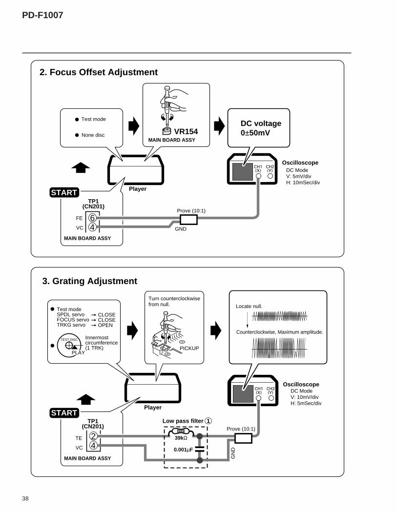
2. Focus Offset Adjustment
Test mode
None disc VR154MAIN BOARD ASSY
DC voltage0±50mV
OscilloscopeDC ModeV: 5mV/divH: 10mSec/div
Prove (10:1)
GND
STARTTP1
(CN201)
Player
3. Grating Adjustment
OscilloscopeDC ModeV: 10mV/divH: 5mSec/div
Player
FE
VC
STARTTP1
(CN201)
TE
VC
Locate null.
Counterclockwise, Maximum amplitude.
39kΩ
0.001µF
Prove (10:1)
GN
D
Low pass filter 1
MAIN BOARD ASSY
MAIN BOARD ASSY
4
Test modeSPDL servoFOCUS servo TRKG servo
= = =
CLOSECLOSEOPEN
TEST DISC Innermostcircumference(1 TRK)
PLAY
Turn counterclockwisefrom null.
PICKUP

PD-F1007
39
1
42
4. Tracking Error Balance Adjustment
Probe (10:1)
VR155
A=B
OscilloscopeDC ModeV: 10mV/divH: 5mSec/div START
TP1(CN201)
Player
TE
VC
39kΩ
0.001µF
Low pass filter 1
Test modeSPDL servoFOCUS servo TRKG servo
= = =
CLOSECLOSEOPEN
TEST DISC
PLAY
Innermostcircumference(1 TRK)
VC
A
B
GND
GN
D
Player
TP1(CN201)
RF
VC
START
Probe (10:1)
OscilloscopeAC ModeV: 20mV/divH: 200nSec/div
NG
OK (Smooth)Eye pattern
5. Pickup 1Radial/ 2Tangential Direction Tilt Adjustment
MAIN BOARD ASSY
MAIN BOARD ASSY
MAIN BOARD ASSY
TEST DISC
PLAY
Test modeSPDL servoFOCUS servo TRKG servo
= = =
CLOSECLOSECLOSE
4
Remove lock tight.
TEST DISC
12
2
1
Position where the screw is visible through the adjustment hole of the float base after moving toward the outer peripheral.

PD-F1007
40
114
6. RF Level Adjustment
VR153
1.2VP-P±0.1V
OscilloscopeAC ModeV: 50mV/divH: 10mSec/div
STARTTP1
(CN201)
Player
RF
VC GND
Prove (10:1)
7. Focus Best Adjustment
OscilloscopeDC ModeCH1: 5mV/divCH2: 20mV/div H: 200ns/div
Prove(10:1)
PlayerSTART TP1(CN201)
RF
VC
MAX
GN
D
Prove(10:1)FE 6
14
GN
D
Adjust the RF level to maximum, with thefocus error voltage within ±150mV.
MAIN BOARD ASSY
MAIN BOARD ASSY
MAIN BOARD ASSY
Test modeSPDL servoFOCUS servo TRKG servo
= = =
CLOSECLOSECLOSE
TEST DISC
PLAY
Innermostcircumference(1 TRK)
VR156MAIN BOARD ASSY
Test modeSPDL servoFOCUS servo TRKG servo
= = =
CLOSECLOSECLOSE
TEST DISC
PLAY
Innermostcircumference(1 TRK)

PD-F1007
41
114
8. RF Level Adjustment
1.2VP-P±0.1V
OscilloscopeAC ModeV: 50mV/divH: 10mSec/div START
TP1(CN201)
Player
RF
VC GND
Prove (10:1)
9. Focus Servo Loop Gain Adjustment
UNDER
OscilloscopeX-Y ModeX: 20mV/divY: 5mV/div
GND
Prove (10:1)
PlayerSTARTTP1
(CN201)
FI
VC
UPPER
JUST
Low-frequencyoscillator
1.2kHz1Vp-p
GN
DG
ND
Prove (10:1)
56kΩ
0.001µF
Low pass filter 2
100kΩ
FE
Make adjustment ifthe value exceedsthe specified range.
Check
654
Lissajous Waveform
MAIN BOARD ASSY
MAIN BOARD ASSY
VR153MAIN BOARD ASSY
Test modeSPDL servoFOCUS servo TRKG servo
= = =
CLOSECLOSECLOSE
TEST DISC
PLAY
Innermostcircumference(1 TRK)
Test modeSPDL servoFOCUS servo TRKG servo
= = =
CLOSECLOSECLOSE
TEST DISC
PLAY
Innermostcircumference(1 TRK) VR152
MAIN BOARD ASSY

PD-F1007
42
11. Focus Servo Loop Gain Adjustment
10. Focus Best Adjustment
OscilloscopeDC ModeCH1: 5mV/divCH2: 20mV/div H: 200ns/div
Prove (10:1)
PlayerSTART TP1(CN201)
RF
VC
MAX
GN
D
Prove (10:1)FE 6
14
GN
D
Readjust ifadjustment is incorrect.
Adjust the RF level to maximum, withthe focus error voltage within ±150mV.
MAIN BOARD ASSY
VR156MAIN BOARD ASSY
Test modeSPDL servoFOCUS servo TRKG servo
= = =
CLOSECLOSECLOSE
TEST DISC
PLAY
Innermostcircumference(1 TRK)
UNDER
OscilloscopeX-Y ModeX: 20mV/divY: 5mV/div
GND
Prove (10:1)
PlayerSTARTTP1
(CN201)
FI
VC
UPPER
JUST
Low-frequencyoscillator
1.2kHz1Vp-p
GN
DG
ND
Prove (10:1)
56kΩ
0.001µF
Low pass filter 2
100kΩ
FE 654
Lissajous Waveform
MAIN BOARD ASSY
Test modeSPDL servoFOCUS servo TRKG servo
= = =
CLOSECLOSECLOSE
TEST DISC
PLAY
Innermostcircumference(1 TRK) VR152
MAIN BOARD ASSY
Check

PD-F1007
43
12. Focus Best Adjustment
OscilloscopeDC ModeCH1: 5mV/divCH2: 20mV/div H: 200ns/div
Prove (10:1)
PlayerSTART TP1(CN201)
RF
VC
MAX
GN
D
Prove (10:1)FE 6
14
GN
D
Adjust the RF level to maximum, withthe focus error voltage within ±150mV.
Adjust this point only if adjustment was made in item 10.
MAIN BOARD ASSY
VR156MAIN BOARD ASSY
Test modeSPDL servoFOCUS servo TRKG servo
= = =
CLOSECLOSECLOSE
TEST DISC
PLAY
Innermostcircumference(1 TRK)
13. Tracking Servo Loop Gain Adjustment
UNDER
OscilloscopeX-Y ModeX: 20mV/divY: 10mV/div
GND
Prove (10:1)
PlayerSTARTTP1
(CN201)
TI
VC
UPPER
JUST
Low-frequencyoscillator
1.2kHz1Vp-p
GN
DG
ND
Prove (10:1)
100kΩ
TE 234
Lissajous Waveform
MAIN BOARD ASSY
Test modeSPDL servoFOCUS servo TRKG servo
= = =
CLOSECLOSECLOSE
TEST DISC
PLAY
Innermostcircumference(1 TRK) VR151
MAIN BOARD ASSY

PD-F1007
44
No. Symbol Name I/O Description
32 P11/ANI1 KBDAT I Keyboard communication datatransmission and reception
33 P10/ANI0 Not used O Open
34 AVDD AVDD – +5V
35 AVREF AVREF – GND
36 P03/INTP3 DCS I Serial communication timing inputfrom the main microcomputer
37 P02/INTP2 KBCLK I Keyboard communication data clockinput
38 P01/INTP0 JOG1 I JOG input 1
39 P00/INTP0/TI0 RMDT I Remote control data input
40 VSS VSS – GND
41 P74| | Not used O OPEN
44 P71
45 P70 JOG2 I JOG input 2
46 VDD VDD – +5V
47 P127/FIP52 STBL O STANDBY–LED
48 P126/FIP51 S36| | | O
54 P120/FIP45 S30
55 P117/FIP44 S29| | | O
62 P110/FIP37 S22Segment output for FL drive
63 P107/FIP36 S21| | | O
70 P100/FIP29 S14
71 P97/FIP28 S13| | | O
78 P90/FIP21 S6
79 VLOAD VLOAD – –30V
80 P87/FIP20 S5| | | O Segment output for FL drive
84 P84/FIP16 S1
85 P83/FIP15 G16| | | O
87 P80/FIP13 G14DIGIToutput for FL drive
88 FIP12 G13| | | O
100 FIP0 G1
No. Symbol Name I/O Description
1 VDD VDD – +5V
2 P37 Not used OOpen
3 P36/BUZ Not used O
4 P35/PCL KD5 I
5 P34/TI2 KD4 I
6 P33/TI1 KD3 IKey data input
7 P32/TO2 KD2 I
8 P31/TO1 KD1 I
9 P30TO0 KD0 I
10 RESET RESET I CPU reset (L: Reset)
11 X2 X2 – Connected to System clock oscillator(4.19 MHz)
12 X1 X1 –
13 IC IC – GND
14 XT2 XT2 – Not Connect (open)
15 P04/XT1 Not used O Only for input: Input of GND
16 VDD VDD – +5V
17 P27/SCK0 Not used O
18 P26/SO0/SB1 Not used OOpen
19 P25/SI0/SB0 Not used O
20 P25/BUSY Not used O
21 P23/STB DREQ O Completion of transmission settingto the main microcomputer
22 P22/SCK1 DCLK I Clock input for serial communicationwith the main microcomputer
23 P21/SO1 KYDT O Serial data output to the main micro-computer
24 P20/SI1 DPDT I Serial data input from the main micro-computer
25 AVSS AVSS – GND
26 P17/ANI7| | Not used O OPEN
30 P13/ANI3
31 P12/ANI2 ACRY O Main microcomputer power ON/OFF
7. GENERAL INFORMATION7.1 PARTS7.1.1 IC
¶ The information shown in the list is basic information and may notcorrespond exactly to that shown in the schematic diagrams.
PD4997A (IC701: DISPLAY BOARD ASSY) Display Control Micro-computer Pin Function

PD-F1007
45
No. Symbol Name I/O Description
31 P16/ANI6 SYNC1 I Synchronization input(pull-up required)
32 P17/ANI7 SYNC3 O Synchronization output
33 AVSS AVSS – GND
34 P130/AN00 Not usedO Output of "L"
35 P131/AN01 Not used
36 AVref1 AVref1 – VDD
37 P70/SI2/RxD SRDT I CD TEXT data input
38 P71/SO2/TxD Not used O Output of "L"
39 P71/SCK2/ASCK SCLK O CD TEXT data fetch clock output
40 Vss Vss – GND
41 P20/SI1 KYDT I Communication data input in regard to the SUB microcomputer
42 P21/SO1 DPDT O Communication data output in regardto the SUB microcomputer
43 P22/SCK1 DCLK O Communication clock in regard tothe SUB microcomputer
44 P23/STB DCS O Communication request output inregard to the SUB microcomputer(H = L: Communication request)
45 P24/BUSY Not used O Output of "L"
46 P25/SI0/SB0 SQSO I Q data serial input (combined use forFCOK/GFS/SENS)
47 P26/SO0/SB1 MDAT O LSI control data serial output
48 P27/SCK0 CLOK O Serial clock
49 P80/A0 A0| | | O
56 P87/A7 A7
57 P40/AD0 A4 O
58 P41/AD1 A12 O
59 P42/AD2 A10 O External RAM address line
60 P43/AD3 A11 O
61 P44/AD4 A9 O
62 P45/AD5 A8 O
63 P46/AD6 A13 O
64 P47/AD7 A15 O
65 P50/A8 IO4| | | O
69 P54/A12 IO8 External RAM data Input/Output
70 P55/A13 IO1 O
PD4996C(IC351: MAIN BOARD ASSY) System Control Micro-computer
No. Symbol Name I/O Description
1 P120/RTP0 DLAT O DAC control data, latch pulse output
2 P121/RTP1 XLAT O LSI control data, latch pulse output
3 P122/RTP2 Not used O Output of "L"
4 P123/RTP3 INSD I Slider INSIDE switch input (L: INSIDE)
5 P124/RTP4 OPEN I Hood open switch input(L: Opening completed)
6 P125/RTP5 CLS I Hood close switch input(L: Closing completed)
7 P126/RTP6 EJCT I Loading out switch input(L: Ejection completed)
8 P127/RTP7 CLMP I Loading mechanism clamping switchinput (L: Clamping completed)
9 IC IC – GND
10 X2 X2 Connected to System clock oscillator– (4.19 MHz)
11 X1 X1
12 VDD VDD – +5V
13 XT2 XT2 – Not Connect (open)
14 P07/XT1 Not used I Input of 5 V (only for input)
15 RESET RESET I CPU reset (L: Reset)
16 P00/INTP0/TI00 DREQ I Communication start request inputfrom the SUD microcomputer(L: Communication start)
17 P01/INTP1/TI01 Not used O Output of "L"
18 P02/INTP2 DPOS I Pulse input for disc position detection
19 P03/INTP3 SCOR I Subcode synchronization S0 + S1 input
20 P04/INTP4 DISC I Disc detection pulse input(L: Disc present)
21 P05/INTP5 Not used O Not used
22 P06/INTP6 DCNT2 I Disc count pulse input 2
23 AVdd AVdd – VDD
24 AVref0 AVref0 – GND
25 P10/ANI0 Not used O Output of "L"
26 P11/ANI1 MUTM O Master side mute output (L: Mute)
27 P12/ANI2 MUTA O Audio muting output (L: Mute)
28 P13/ANI3 Not used O Output of "L"
29 P14/ANI4 MSIN I Master input (response from the slave)
30 P15/ANI5 KYCON O Keyboard power supply control(H: Power ON)
Pin Function

PD-F1007
46
No. Symbol Name I/O Description
71 Vss Vss – GND
72 P56/A14 IO2O External RAM data Input/Output
73 P57/A15 IO3
74 P60 SCHK I Input for slave judgment (L: Slave)
75 P61 MCHK I Input for master judgment (L: Master)
76 P62 Not usedO Output of "L"
77 P63 Not used
78 P64/RD A16 O External RAM address line
79 P65/WR WE O Write control output (L: Write)
80 P66/WAIT CS O External RAM chip selection output(H: Standby)
81 P67/ASTB RD O Read control output (L: Read)
82 P100/TI5/TO5 MUTS O Slave side mute output (L: Mute)
83 P101/TI6/TO6 DSLT O Selector outputCount-up (DSRT: L, DSLT: H)
84 P102 DSRT O Count-down (DSRT: H, DSLT: L)Stopped (DSRT: L, DSLT: L)
85 P103 MOPN O Door motor outputOpen (MOPN: H, MCLS: L)
86 P30/TO0 MCLS O Close (MOPN: L, MCLS: H)Stop (MOPN: L, MCLS: L)
No. Symbol Name I/O Description
87 P31/TO1 LIN O Output for loading motorIN (LIN: H, LOUT: L)
88 P32/TO2 LOUT O OUT (LIN: L, LOUT: H)Stop (LIN: L, LOUT: L)
89 P33/TI1 LDON O Laser diode output (H: ON, L: OFF)
90 P34/TI2 XRST O Reset output for each LSI
91 P35/PCL TRST O CD TEXT decoder IC reset output(L: Reset)
92 P36/BUZ CLED O Center LED lighting control (H: Lit)
93 P37 PLED O Sensor output for disc detection(H: Lit)
94 P90 Not used O Output of "L"
95 P91 TRST I Test mode input for checker (H: Test)
96 P92 MSOT O Master control output (control of theslave)
97 P93 SLOT O Slave output (response to the master)
98 P94 HBIT I Hi-bit correspondence switchinginput (H: Hi-bit correspondence)
99 P95 TEST I Test mode switching input(H: Test mode)
100 P96 DQSY I CD TEXT data timing input
M5M51008BFP–70LL (IC352: MAIN BOARD ASSY) S-RAM
Block Diagram
3128 A
ddre
ss In
put B
uffe
r
Row
Dec
oder 131072 Words
× 8 bits
1024 Rows× 128 Columns
× 8 Blocks Out
put B
uffe
r
Sen
se A
mp.
A4A5A6A7
A12A14A16A15A13
8765432
21
191817151413
20
29
2230
24
DQ1DQ2DQ3DQ4DQ5DQ6DQ7DQ8
A8
32 VCC (5V)
16 GND (0V)
OE
S1S2
27
1012
Add
ress
Inpu
tB
uffe
rA
ddre
ss In
put
Buf
fer
A0A2A3 9
A10 23
2526
11
Col
umn
Dec
oder
Blo
ckD
ecod
er
Clock Generator
Dat
a In
put B
uffe
r
A1A11A9
W

PD-F1007
47
98 50
1 49
1–1
1–2
1–3
1–4
1–5
1–6
1–7
2–1
2–2
2–3
2–4
2–5
2–6
2–7
3–1
3–2
3–3
3–4
3–5
3–6
3–7
4–1
4–2
4–3
4–4
4–5
4–6
4–7
5–1
5–2
5–3
5–4
5–5
5–6
5–72a 1a
3a 2a 1a 3a 2a 1a 3a col 2a 1a
1f 1b1g
1e 1c1d
(1G to 12G)
1G 2G
15G 14G 13G
3G 4G 5G 6G 7G 8G 9G 10G 11G 12G
P1
1G to 12G 13G 14G 15G 16G
P2
P3
P4
P5
P6
P7
P8
P9
P10
P11
P12
P13
P14
P15
P16
P17
P18
1–1
2–1
3–1
4–1
5–1
1–2
2–2
3–2
4–2
5–2
1–3
2–3
3–3
4–3
5–3
1–4 –––
–––
2–4
3–4
1d
1e
1c
1g
1f
1b
1a
1d
1e
1c
1g
1f
1b
1a
1d
1e
1c
1g
1f
1b
1a 1d
1e
1c
1g
1f
1b
1a
col
2d
2e
2c
2g
2f
2b
2a
2d
2e
2c
2g
2f
2b
2a
2d
2e
2c
2g
2f
2b
2a
3d
3e
3d
3e
3d
3e
2d
2e
P19
1G to 12G 13G 14G 15G 16G
P20
P21
P22
P23
P24
P25
P26
P27
P28
P29
P30
P31
P32
P33
P34
P35
P36
4–4
5–4
1–5
2–5
3–5
4–5
5–5
1–6
2–6
3–6
4–6
5–6
1–7
2–7
3–7
4–7
5–7
–––
–––
–––
–––
–––
–––
–––
–––
–––
–––
–––
–––
–––
–––
–––
–––
–––
–––
–––
–––
–––
–––
–––
–––
–––
–––
–––
–––
–––
–––
–––
–––
–––
–––
–––
–––
–––
–––
–––
–––
–––
–––
3c
3g
3f
3b
3a
3c
3g
3f
3b
3a
3c
3g
3f
3b
3a
2c
2g
2f
2b
2a
Pin ConnectionPin Assignment
Grid Assignment
Anode Connection
PIN NO.
CONNECTION
98
97
96
95
94
93
92
91
90
89
88
87
86
85
84
83
82
81
80
79
78
77
76
75
74
73
72
71
70
69
68
67
66
F1
F1
F1
F1
NP
NP
13G
12G
11G
10G
P36
P35
P34
9G
8G
7G
6G
5G
4G
3G
2G
1G
NX
NX
NX
NX
NX
NX
NX
NX
NX
NX
NC
PIN NO.
CONNECTION
65
64
63
62
61
60
59
58
57
56
55
54
53
52
51
50
49
48
47
46
45
44
43
42
41
40
39
38
37
36
35
34
33
P33
P12
P11
P10
16G
15G
14G
NX
NX
NX
NX
NX
NX
NX
NX
NX
NX
P9
P8
P7
P6
P5
P4
P3
P2
P1
IC
NP
NP
F1
F1
F1
F1
P32
P31
P30
P29
P28
P27
P26
P25
P24
P23
P22
P21
P20
P19
P18
P17
P16
P15
P14
P13
NP
NP
NP
NP
F2
F2
F2
F2
F2
F2
F2
F2
PIN NO.
CONNECTION
32
31
30
29
28
27
26
25
24
23
22
21
20
19
18
17
16
15
14
13
12
11
10 9 8 7 6 5 4 3 2 1
Note 1) F1, F2 ...... Filament 5) DL .................... Datum Line2) NP ............ No Pin 6) 1G to 16G ........ Grid3) NX ............ No extend Pin 7) IC ..................... Internal Connection4) NC ........... No Connection
7.1.2 DISPLAY PEL1096 (V701: DISPLAY BOARD ASSY) Vacuum Fluorescent Display

PD-F1007
48
7.2 DIAGNOSIS7.2.1 DISASSEMBLY
3
3
3
22
CN401
CN205CN203
CN208
CN202
CN207
CN204 CN11
CN351
MAIN BOARD ASSY
Screw A (× 6)
Screw A
Screw A
Screw A
Rear Base
Screw A3
4
Hook
Hood
Open
Center Pole
Screw B (× 5)
5
5Arm Assy
Screw C
Link D
Screw C
Front
Removal of the Servo Mechanism Assy GM
1 Remove the Bonnet. (Left and rightside: ×2, rear side: ×3)
2 Remove the wires from the MAINBOARD Assy. (9 places)
3 Remove the screws A (10 screws), andremove the MAIN BOARD Assy.
Note) When the screws (6 screws) areremoved in this condition, themechanical unit can be removed asone entity. Refer to "2. EXPLODEDVIEWS AND PARTS LIST".
4 Open the Hood, remove the screws B
(5 screws), disconnect the hooks ofFront Panel Assy and Hood (3 places),and remove the Center Pole.
5 Remove the screws C (3 screws),remove the link section D, and removethe Arm Assy.

PD-F1007
49
6
Front
Disc Guard Screw E(× 4)
Connector Assy (4P)
Flexible Flat Cable
Screw G
Float Spring
Float Base AssyFloat Base
Float Rubber
Servo MechanismAssy GM
10 8
89
11
6 Remove the screws E (4 screws), and then remove the Disc Guard.7 Remove the Float Base Assy and Clamp Holder.
8 Remove the Flexible Flat Cableand the Connector Assy (4P)from the Float Base.
9 Remove the screw G.0 Remove the float spring.
(To install this part, line up thefloat angle side of the ServoMechanism ASSY GM first, andpress down on the float base side.)
- Remove the float rubber fromthe Servo Mechanism ASSYGM. At this time the FloatRubber should remain on theFloat Base side. (To install it onthe Float Base when it has beenremoved, push it into place witha thin cylindrical object.
7
7
Front
Clamp Support
Clamp Holder
ClampSpring
Float Base Assy

PD-F1007
50
Disc Rack
Screw A (× 2)
Gear Holder Assy
2
3
Front Panel Assy
Hood
Disconnectthe Hook
Hood Base Assy
Screw B
3
2
Screw B
2
Screw B
2
Disconnect the Hook
Disconnectthe Hooks
1 Perform the steps 1 to 6 of " Removal of the Servo MechanismAssy GM ".
2 Remove the screws A (2 screws), and then remove the Gear HolderAssy.
3 Remove the Disc Rack.
Removal of the Gear Holder Assy and the Disc Rack
1 Perform the steps 1 to 6 of " Removal of theServo Mechanism Assy GM ". and the steps 2 and3 of " Removal of the Gear Holder Assy and theDisc Rack".
2 Remove the screws B (3 screws), and then removethe Front Panel Assy.
3 Slide the Hood to the left side and remove it.4 Remove the screws C (2 screws) and remove the
Hood Base Assy.
Removal of the Hood and HoodBase Assy
Hood Base Assy
4Screw C
(× 2)
PD-F1007
51
UserDisplay Display Contents
None • Disc playing was tried after loading, butthe disc could not be detected becausethere was no disc,the disc was upside down,the disc was dirty, disc loading had notbeen completed, etc.
• Focus was lost during disc playingbecause of disc scratches, dirt, etc.
None • At the time of track selection during play,or when trying to play, the servomechanism could not move to the positionof the intended track within a fixed time.
• Disc loading was tried, but loading wasnot possible within a fixed time. (The discwas not brought from the rack.)
• It was tried to return the disc to the rack,but the disc could not be returned withina fixed time.
• At the time of disc selection during play,or at the start of play from stoppedcondition, the selection mechanism couldnot move to the position of the intendeddisc within a fixed time.
• After initialization of the selectionmechanism, after selection mechanismNG, etc., forced rack section positiondetection is performed for the selectionmechanism, but detection was notpossible within a fixed time.
None • Playing was tried after disc loading, butnormal disc rotation was not possiblebecausethe disc was upside down,the disc was dirty,disc loading had not been completed, etc.
• During play normal rotation was notpossible because of disc scratches, dirt,etc.
Display Contents
During spindle stop operation
During disc return
During disc selection (during clamping operationat the time of 26)
During setup
During CDR setup operation
During TOC reading
During search operation on the disc
During play operation
During pause operation
During manual search
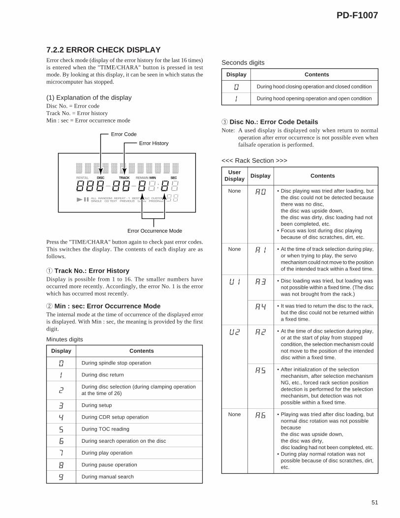
7.2.2 ERROR CHECK DISPLAY
Error Code
Error History
Error Occurrence Mode
Error check mode (display of the error history for the last 16 times)is entered when the "TIME/CHARA" button is pressed in testmode. By looking at this display, it can be seen in which status themicrocomputer has stopped.
(1) Explanation of the displayDisc No. = Error codeTrack No. = Error historyMin : sec = Error occurrence mode
Press the "TIME/CHARA" button again to check past error codes.This switches the display. The contents of each display are asfollows.
1 Track No.: Error HistoryDisplay is possible from 1 to 16. The smaller numbers haveoccurred more recently. Accordingly, the error No. 1 is the errorwhich has occurred most recently.
2 Min : sec: Error Occurrence ModeThe internal mode at the time of occurrence of the displayed erroris displayed. With Min : sec, the meaning is provided by the firstdigit.
Minutes digits
Display Contents
During hood closing operation and closed condition
During hood opening operation and open condition
Seconds digits
3 Disc No.: Error Code DetailsNote: A used display is displayed only when return to normal
operation after error occurrence is not possible even whenfailsafe operation is performed.
<<< Rack Section >>>

PD-F1007
52
UserDisplay Display Contents
None • When the position of the selectionmechanism just before switching to discselection operation os DCNT terminal ="L". (Normally, DCNT terminal = "H"exists when the selection mechanism isstopped, so that it can be assumed thatthe position of the mechanism hasdeviated for some reason. There is thepossibility that a position deviation of themechanism can cause a defect of themechanism.)
None • At the time of movement of the selectionmechanism, a deviation has occurredbetween the present position of the discand the disc position according to positiondetection. (It can be assumed that thewaveform at the DCNT terminal and/orat the DPOS terminal has beenmiscounted. When a miscount occurs, adiscrepancy occurs between thedisplayed disc No. and the counted discposition.)
None • When the position of the mechanismbecame DCNT terminal = "L" during discloading. (Normally, DCNT terminal = "H"exists when the selection mechanism isstopped, so that it can be assumed thatthe position of the mechanism hasdeviated for some reason. There is thepossibility that a position deviation of themechanism can cause a defect of themechanism.)
None • At the time of shifting to a different discafter play completion, the pickup doesnot return to the innermost circumference.
<<< Rack section >>>
UserDisplay Display Contents
The hood did not open within a fixed time.The hood switch was broken.
The hood did not close within a fixed time.The hood switch was broken.
None It was tried to force the closed hood open.The hood switch was broken.
<<< Hood Section >>>
7.2.3 EXPLANATION OF DISC DETECTION1. Detection of the rack positionThere are two types of slits on the rear of the rack, and theircombination is used to find which disc has been selected duringrack rotation. The input ports (DCNT, DPOS) are as follows.
Disc No. 3 4 5 6 7 8 9 10 11 12 13 14 15 16 17 181 2DCNTDPOS
Disc No. 21 22 23 24 25 26 27 28 29 30 31 32 33 34 35 3619 20DCNTDPOS
Disc No. 39 40 41 42 43 44 45 46 47 48 49 50 51 52 53 5437 38DCNTDPOS
Disc No. 57 58 59 60 61 62 63 64 65 66 67 68 69 70 71 7255 56DCNTDPOS
Disc No. 75 76 77 78 79 80 81 82 83 84 85 86 87 88 89 9073 74DCNTDPOS
Disc No. 93 94 95 96 97 98 99 100 101 102 103 104 105 106 107 10891 92DCNTDPOS
Disc No. 111 112 113 114 115 116 117 118 119 120 121 122 123 124 125 126109 110DCNTDPOS
Disc No. 129 130 131 132 133 134 135 136 137 138 139 140 141 142 143 144127 128DCNTDPOS
Disc No. 147 148 149 150 151 152 153 154 155 156 157 158 159 160 161 162145 146DCNTDPOS
Disc No. 165 166 167 168 169 170 171 172 173 174 175 176 177 178 179 180163 164DCNTDPOS
Disc No. 183 184 185 186 187 188 189 190 191 192 193 194 195 196 197 198181 182DCNTDPOS
Disc No. 201 202 203 204 205 206 207 208 209 210 211 212 213 214 215 216199 200DCNTDPOS

PD-F1007
53
Disc No. 219 220 221 222 223 224 225 226 227 228 229 230 231 232 233 234217 218DCNTDPOS
Disc No. 237 238 239 240 241 242 243 244 245 246 247 248 249 250 251 252235 236DCNTDPOS
Disc No. 255 256 257 258 259 260 261 262 263 264 265 266 267 268 269 270253 254DCNTDPOS
Disc No. 273 274 275 276 277 278 279 280 281 282 283 284 285 286 287 288271 272DCNTDPOS
Disc No. 291 292 293 294 295 296 297 298 299 300 301 302 303 S.L
S.L (304): SINGLE LODER
305 306289 290DCNTDPOS
Disc No. 2 3 4 5 6 7 8 9 10 11 12 13 14 15 16 17307 1DCNTDPOS
1 The microcomputer looks every 1 msec at the status (H or L) ofthe two inputs DCNT and DISC.
2 8 msec (A in the figure) after the drop of DCNT (C in the figure),the last 17 DISC inputs (B in the figure) are checked.A disc is assumed to be resent when even one of them is "L".
3 No disc is assumed when DISC was "H" all 17 times (B in thefigure) in 2.
Note: In regard to the drop ( ) of DCNTFor looking at the drop or rise of DCNT, it is necessary to checkDCNT every 1 msec for "H" or "L".
"H" = "L" means a drop ( )."L" = "H" means a rise ( ).
For the timing, either one of the following A and B can be assumed.Accordingly, the point where a drop is found differs by max. 1 msecfor A and B.Thus, using the above figure, it can be said that the time fromfinding that a drop has occurred until starting to check for discpresence (A in the above figure) becomes 8 to 9 msec.
Relation between input port DCNT, DPOSand position of the mechanism
2. Position relation between position of the rackmechanism and photocell for disc detection
The relation between these two positions is as follows.
Fig.: The rack seen from above
The position of the mechanism and the photocell for detection areoffset by a distance corresponding to 9 discs. Accordingly, thephotocell for detection sees the disc number 9 discs before theposition of the mechanism.
Example: Disc No. at the rack position : Disc No. 100Disc No. seen by the photocell for detection
: Disc No. 91
Note: The rack has 307 slits, but the slits 301 to 303 and 304 to 307are the space for the side of the single loader and are not used.Disc detection also is not performed for them.
3. Disc Detection Method3-1 In Regard to the Disc Detection Method
Disc detection is performed after stabilization of the rotationspeed after rack rotation start and completion of acceleration.(After start of rotation, detection starts after feed of 20 discs.)The input ports DCNT and DISC of the microcomputer are usedfor disc detection.
Port Explanation : DCNT : As described above.DISC : Input of the disc detection result
by the photocell for disc detection.Input value "H" : No disc,
"L" : Disc present
3-2 In Regard to the Disc Detection Timing
C
DCNT
DISC
A(8msec)
B(16msec)
A B
"H" "L" "H" "L"
1msec 1msec
Photocell for detection
Position of themechanism

PD-F1007
54
7.3 BLOCK DIAGRAM
PICKUPAssembly
SERVOCONTROLLER
IC151CXA1782CQ
DECODER+ DACIC301
CXD2529Q
S-RAMIC352
M5M51008BPF-70LL
LPFIC405
NJM4558D-DLINEOUT
CPUIC351
PD4996C
AMP
IC201IC202
LA6520SpindleCarriageLoadingDisc Select
FocusTracking
M
DISPLAYFUNCTION KEY POWER SUPPLY
.
.
.
.
.
.TEXT ENCODER
IC302LC89170M
CPUDISPLAY CONTROL
IC701PD4997A
BufferIC407, IC408NJM4558D-D
H.P. BufferIC406
M5218AFP
SLAVEAUDIO IN
PD-F1007
55
KEYBORDINPUT
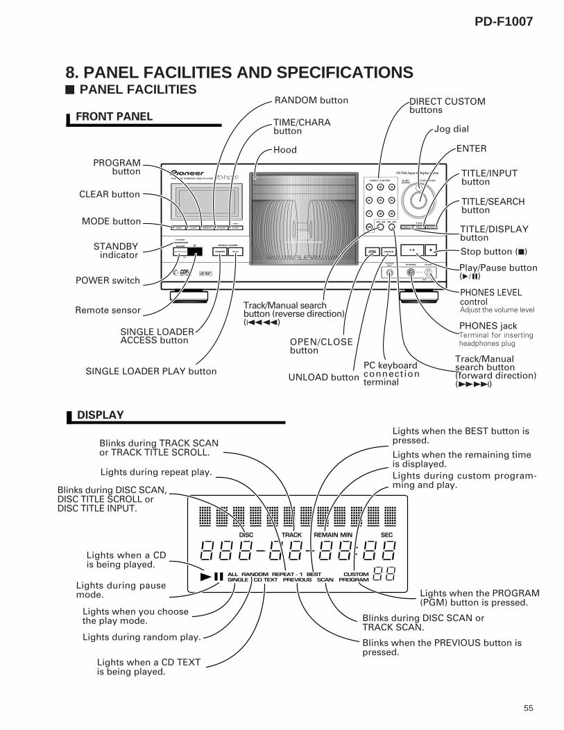
8. PANEL FACILITIES AND SPECIFICATIONS PANEL FACILITIES
FRONT PANEL
Lights when the BEST button ispressed.
Lights when the remaining timeis displayed.
Lights during random play.
Lights during repeat play.
Lights when the PROGRAM(PGM) button is pressed.
Lights when a CDis being played.
Lights during pausemode.
Blinks when the PREVIOUS button ispressed.
Blinks during DISC SCAN,DISC TITLE SCROLL orDISC TITLE INPUT.
Lights during custom program-ming and play.
Lights when you choosethe play mode.
DISPLAY
POWER switch
SINGLE LOADERACCESS button
Hood
Remote sensor
PROGRAMbutton
PHONES jackTerminal for insertingheadphones plug
PHONES LEVELcontrolAdjust the volume level
Track/Manualsearch button(forward direction)(¡¢)
RANDOM button
OPEN/CLOSEbutton
UNLOAD button
MODE button
CLEAR button
SINGLE LOADER PLAY button
STANDBYindicator Stop button (7)
Play/Pause button(6)
Track/Manual searchbutton (reverse direction)(41)
TITLE/DISPLAYbutton
TITLE/SEARCHbutton
TITLE/INPUTbutton
TIME/CHARAbutton Jog dial
DIRECT CUSTOMbuttons
Blinks during TRACK SCANor TRACK TITLE SCROLL.
Blinks during DISC SCAN orTRACK SCAN.
Lights when a CD TEXTis being played.
ENTER
PC keyboardconnectionterminal

PD-F1007
56
SPECIFICATIONS3. INPUT Output terminalAudio line outputCD • DECK SYNCHRO jackOptical digital output jackHeadphone jack with volume controlMASTER/SLAVE Control input/output jackSLAVE Audio inputPC keyboard input jack
4. Accessories÷ Remote control unit .................................................................. 1÷ Size AA/R6P dry cell batteries ................................................... 2÷ Audio cable ............................................................................... 1÷ Control cable ............................................................................. 1÷ Keyboad label ............................................................................ 1÷ Operating instructions ............................................................... 1
Note!!
Specifications and design subject to possible modification withoutnotice, due to improvements.
1. GeneralType ...........................................Compact disc digital audio systemPower requirements ................................ AC 220V-230V, 50/60 HzPower consumption ................................................................. 16WPower consumption in standby mode ....................................... 2WOperating temperature ............................................... +5°C - +35°C
(+41°F - +95°F)Weight ( without package ) ................................. 8.0 kg (17 lb 6 oz.)External dimensions ......................... 420(W) X 433(D) X 193(H) mm
16-9/16(W) X 17-1/16(D) X 7-5/8(H) in.
2. Audio sectionFrequency response ................................................... 2 Hz - 20 kHzS/N ratio ........................................................ 105 dB or more (EIAJ)Dynamic range ................................................ 96 dB or more (EIAJ)Harmonic distortion ....................................... 0.003 % or less (EIAJ)Level difference between channels ................. 1.0 dB or less (EIAJ)Output voltage .................................................. 2 ± 0.3 Vrms (EIAJ)Wow and flutter ............................... less than ±0.001 % (W.PEAK)
( below measurable level ) (EIAJ)Channels ............................................................ 2-channel ( stereo )
Remote control unit x 1(CD-PD094)(PWW1139)
Size AA/R6P dry cellbatteries x 2
Audio cable x 1(PDE1248) (L=1 m)
Control cable x 1(PDE1247) (L=1 m)
Other included items÷ Keyboad label÷ Warranty card÷ Operating Instructions
Accessories
White
RedBlack


