
Ferroelectric HfO2 Thin Films May 12th, 2015 JACKSON ANDERSON
ELECTRICAL AND MICROELECTRONIC ENGINEERING
ROCHESTER INSTITUTE OF TECHNOLOGY

Outline Introduction ◦Background ◦ Project Objectives
Experimental Results ◦Deposition of Doped HfO2 Thin Films ◦CV Measurements ◦Hysteresis Measurements
Conclusions and Future Research
2/5/2016 JACKSON ANDERSON - FERROELECTRIC HFO2 THIN FILMS 2

Outline Introduction Experimental Results Conclusions and Future Research
2/5/2016 JACKSON ANDERSON - FERROELECTRIC HFO2 THIN FILMS 3

What is Ferroelectricity?
2/5/2016 JACKSON ANDERSON - FERROELECTRIC HFO2 THIN FILMS 4

Measurements of Ferroelectricity
2/5/2016 JACKSON ANDERSON - FERROELECTRIC HFO2 THIN FILMS 5
Pr-
Pr+
Vc+ Vc-
Remnant Polarization: ◦ Polarization in ferroelectric
material when no bias applied
Coercive Voltage/Field: ◦ Voltage/E-field when no
polarization is present

Benefits of Ferroelectric Memory (FeFET)
Sub-100ns read/write times (Yurchuk, 2014)
Smaller footprint than DRAM ◦ 1T vs 1T1C
Potential for use in non-volatile applications ◦ Memory window of over 1V shown after 10 days (HfO2) (Yurchuk, 2014)
◦ 10 year memory window projected for HfO2 and traditional materials (ITRS, 2013)
◦ Lower write voltages than floating gate or charge-trap memories ◦ 4-6 V vs 10-15 V required for floating gate (Yurchuk, 2014)
Non-charge based
2/5/2016 JACKSON ANDERSON - FERROELECTRIC HFO2 THIN FILMS 6
Arimoto, 2004

Challenges with Traditional Ferroelectric Materials
Lead zirconate titanate (PZT) and strontium bismuth tantalate (SBT) most common ferroelectric films
These films likely not scalable beyond 22 nm node ◦ Low coercive field requires thick ferroelectric layer to obtain useful memory
window ◦ Thick buffer layer required between ferroelectric gate and channel to limit
inter-diffusion ◦ Depolarization field caused by buffer layer decreases retention time
2/5/2016 JACKSON ANDERSON - FERROELECTRIC HFO2 THIN FILMS 7
ITRS, 2013

Why HfO2? Higher coercive field allows for thin ferroelectric layer, enabling continued scaling of FeFETs
Doesn’t require thick buffer layer – decreases depolarization field, increasing theoretical retention time
Familiar material – can leverage high-k metal gate (HKMG) process knowledge
2/5/2016 JACKSON ANDERSON - FERROELECTRIC HFO2 THIN FILMS 8
Yurchuk et al, 2014.
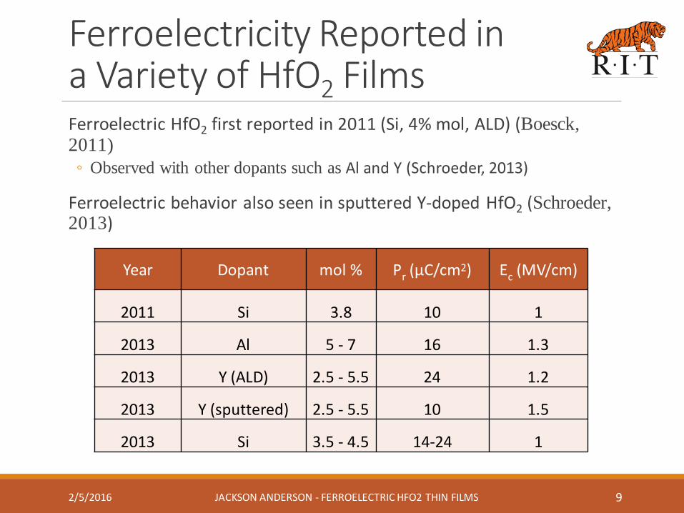
Ferroelectricity Reported in a Variety of HfO2 Films
Ferroelectric HfO2 first reported in 2011 (Si, 4% mol, ALD) (Boesck, 2011) ◦ Observed with other dopants such as Al and Y (Schroeder, 2013)
Ferroelectric behavior also seen in sputtered Y-doped HfO2 (Schroeder, 2013)
2/5/2016 JACKSON ANDERSON - FERROELECTRIC HFO2 THIN FILMS 9
Year Dopant mol % Pr (μC/cm2) Ec (MV/cm)
2011 Si 3.8 10 1
2013 Al 5 - 7 16 1.3
2013 Y (ALD) 2.5 - 5.5 24 1.2
2013 Y (sputtered) 2.5 - 5.5 10 1.5
2013 Si 3.5 - 4.5 14-24 1

Project Objectives
1. Develop a process for fabrication of ferroelectric HfO2 devices using tools available in the RIT Semiconductor and Microsystems Fabrication Laboratory (SMFL)
◦ Sputtered HfO2 film (no Atomic Layer Deposition)
2. Enable in-house characterization of ferroelectric films through the installation and qualification of a newly purchased ferroelectric test system
2/5/2016 JACKSON ANDERSON - FERROELECTRIC HFO2 THIN FILMS 10

Outline Introduction Experimental Results Conclusions and Future Research
2/5/2016 JACKSON ANDERSON - FERROELECTRIC HFO2 THIN FILMS 11

Previous RIT Work
2/5/2016 JACKSON ANDERSON - FERROELECTRIC HFO2 THIN FILMS 12
M. Witulski, Senior Design 2014.

CV Window Changes with Sweep Speed
Window in CV likely caused by charges rather than ferroelectricity
2/5/2016 JACKSON ANDERSON - FERROELECTRIC HFO2 THIN FILMS 13

HfO2/Al Sandwich Approach for More Uniform Doping
HfO2/Al deposited via alternating sputter without breaking vacuum
Some devices exhibited mechanical failure of film stack after anneal ◦ Additional layers added stress to the system ◦ Additional interfaces provided more points for failure
2/5/2016 JACKSON ANDERSON - FERROELECTRIC HFO2 THIN FILMS 14
Al
Al 10 nm
15 nm
600 nm

Al Solid Source Doping Revisited
10 nm TiN Reactive Sputter (D1,D2) 15 nm HfO2 Reactive Sputter (all wafers) 5 nm Aluminum Layer ◦ Evaporation (D1, D4) ◦ Sputtering (D2, D3)
Sputter & Lift-off Top 10 nm TiN (half of each wafer) Anneal – RTA or Furnace Evaporate & Lift-off Top Al (600 nm) Evaporate Back Al (600 nm)
2/5/2016 JACKSON ANDERSON - FERROELECTRIC HFO2 THIN FILMS 15
Al
TiN
Si p-type (100)
Al HfO2
Al
Al
TiN
Si p-type (100)
Al HfO2
Al
TiN
Al
Si p-type (100)
Al
HfO2
Al
TiN
Al
Si p-type (100)
Al
HfO2
Al
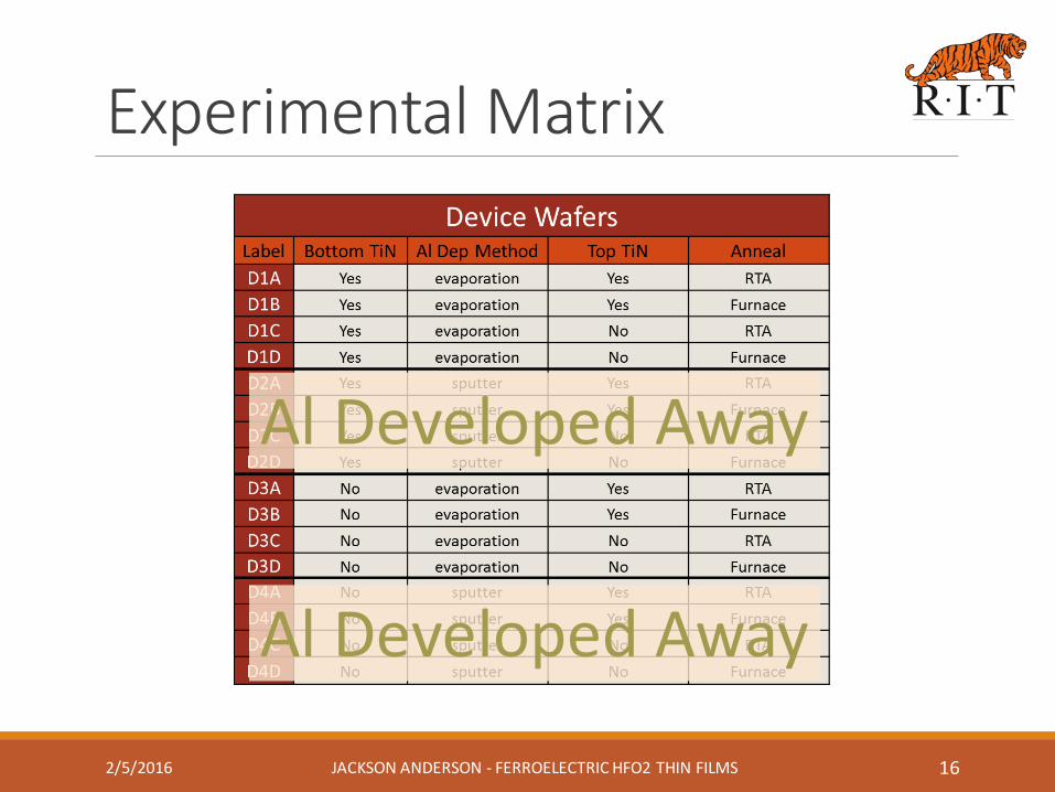
Experimental Matrix
2/5/2016 JACKSON ANDERSON - FERROELECTRIC HFO2 THIN FILMS 16
Al Developed Away
Al Developed Away

Promising Results Seen in Samples with TiN Cap
2/5/2016 JACKSON ANDERSON - FERROELECTRIC HFO2 THIN FILMS 17
Furnace - 1hr 600°C
RTA - 20s 850°C
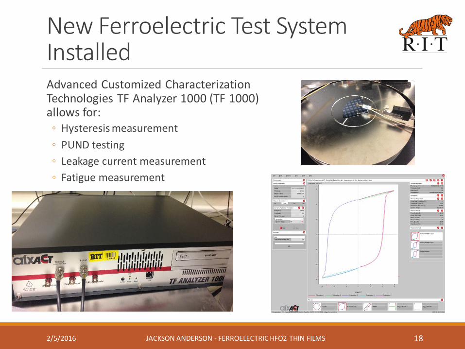
New Ferroelectric Test System Installed
Advanced Customized Characterization Technologies TF Analyzer 1000 (TF 1000) allows for: ◦ Hysteresis measurement ◦ PUND testing ◦ Leakage current measurement ◦ Fatigue measurement
2/5/2016 JACKSON ANDERSON - FERROELECTRIC HFO2 THIN FILMS 18

Discrete Component Measurement
2/5/2016 JACKSON ANDERSON - FERROELECTRIC HFO2 THIN FILMS 19
Evans, 2008

NaMLab Ferroelectric and Antiferroelectric HfO2
2/5/2016 JACKSON ANDERSON - FERROELECTRIC HFO2 THIN FILMS 20
Voltage (V)
-3 -2 -1 0 1 2 3
Pol
ariz
atio
n uC
/cm
2
-30
-20
-10
0
10
20
308 GE AFE Sample 200Hz 3V
Voltage (V)
-3 -2 -1 0 1 2 3
Pol
ariz
atio
n uC
/cm
2
-25
-20
-15
-10
-5
0
5
10
15
20
259 GE FE Sample 100Hz 3V
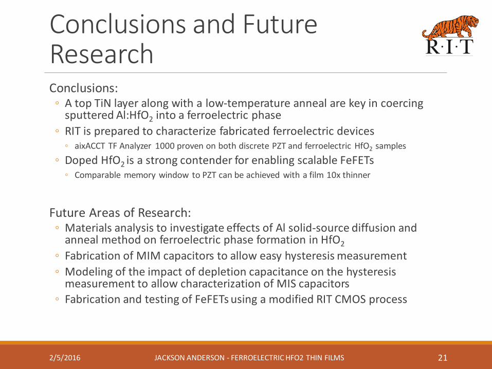
Conclusions and Future Research
Conclusions: ◦ A top TiN layer along with a low-temperature anneal are key in coercing
sputtered Al:HfO2 into a ferroelectric phase ◦ RIT is prepared to characterize fabricated ferroelectric devices
◦ aixACCT TF Analyzer 1000 proven on both discrete PZT and ferroelectric HfO2 samples
◦ Doped HfO2 is a strong contender for enabling scalable FeFETs ◦ Comparable memory window to PZT can be achieved with a film 10x thinner
Future Areas of Research: ◦ Materials analysis to investigate effects of Al solid-source diffusion and
anneal method on ferroelectric phase formation in HfO2 ◦ Fabrication of MIM capacitors to allow easy hysteresis measurement ◦ Modeling of the impact of depletion capacitance on the hysteresis
measurement to allow characterization of MIS capacitors ◦ Fabrication and testing of FeFETs using a modified RIT CMOS process
2/5/2016 JACKSON ANDERSON - FERROELECTRIC HFO2 THIN FILMS 21

Acknowledgements Karine Florent and Dr. Santosh Kurinec
Dr. Dale Ewbank and Dr. Robert Pearson
Dr. Uwe Schroeder, NaMLab
Dr. Lutz Wilde, Fraunhofer Institute for Photonic Microsystems (IPMS)
Dr. Stephan Tiedke, President aixACCT Systems GmbH
Matt Filmer, Dr. Michael Jackson, and Dr. Karl Hirschman
The entire SMFL Staff
2/5/2016 JACKSON ANDERSON - FERROELECTRIC HFO2 THIN FILMS 22
This work was supported in part by the National Science Foundation, Grant # ECCS-1541090 Any opinions, findings, and conclusions or recommendations expressed in this material are those of the author(s) and do not necessarily reflect the views of the National Science Foundation.
References [1] E. Yurchuk, et al., "Impact of Scaling on the Performance of HfO2-Based Ferroelectric Field Effect Transistors,"Ieee Transactions on Electron Devices, vol. 61, pp. 3699-3706, Nov 2014.
[2] ITRS Emerging Research Devices, pp. 12, 2013 http://www.itrs.net/Links/2013ITRS/2013Chapters/2013ERD.pdf
[3] Y. Arimoto and H. Ishiwara, "Current status of ferroelectric random-access memory," Mrs Bulletin, vol. 29, pp. 823-828, Nov 2004.
[4] T. S. Boescke, J. Muller, D. Brauhaus, U. Schroder, and U. Bottger, "Ferroelectricity in hafnium oxide thin films," Applied Physics Letters, vol. 99, p. 3, Sep 2011.
[5] U. Schroeder, S. Mueller, J. Mueller, E. Yurchuk, D. Martin, C. Adelmann, et al., "Hafnium Oxide Based CMOS Compatible Ferroelectric Materials," Ecs Journal of Solid State Science and Technology, vol. 2, pp. N69-N72, 2013.
[6] Evans, Joe T. “Typical Performance of Packaged ‘AB’ Capacitors,” Radiant Technologies, Inc. 2008.
2/5/2016 JACKSON ANDERSON - FERROELECTRIC HFO2 THIN FILMS 23

Thank You.
2/5/2016 JACKSON ANDERSON - FERROELECTRIC HFO2 THIN FILMS 24

Backup
2/5/2016 JACKSON ANDERSON - FERROELECTRIC HFO2 THIN FILMS 25

Dynamic Hysteresis Measurement (DHM)
2/5/2016 JACKSON ANDERSON - FERROELECTRIC HFO2 THIN FILMS 26

Discrete Ferroelectric Capacitor Structure
2/5/2016 JACKSON ANDERSON - FERROELECTRIC HFO2 THIN FILMS 27
Evans, 2008
100 nm Pt Electrode
150 nm Pt Electrode 255 nm PZT
Ferroelectric Film 250 nm PZT for protection
500nm SiO2 as a foundation
550 µm Si Wafer

Doped Capacitors After Anneal
2/5/2016 JACKSON ANDERSON - FERROELECTRIC HFO2 THIN FILMS 28
850°C 20s
1000°C 20s

Undoped Shadow Mask Reference Capacitors
P-type 111 wafers
Anneal ◦ Wafer 1: 1000 C ◦ Wafer 2: 870 C (850 target) ◦ Wafer 3: 740 C (700 target)
2/5/2016 JACKSON ANDERSON - FERROELECTRIC HFO2 THIN FILMS 29
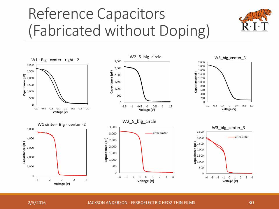
Reference Capacitors (Fabricated without Doping)
2/5/2016 JACKSON ANDERSON - FERROELECTRIC HFO2 THIN FILMS 30
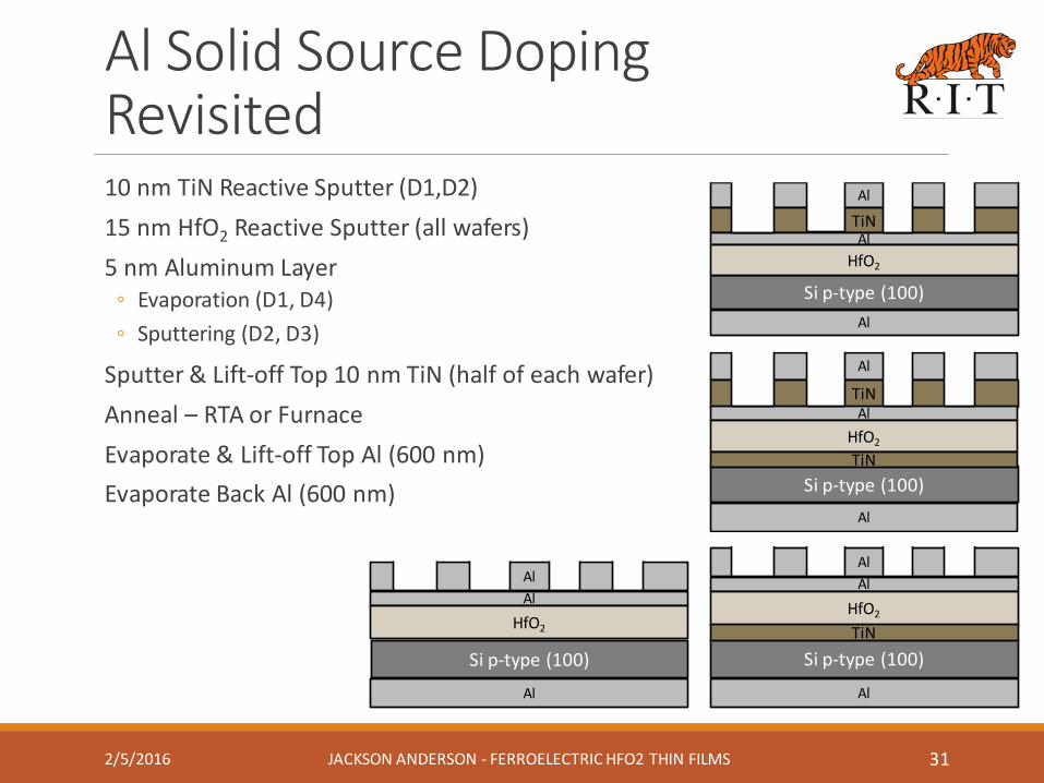
Al Solid Source Doping Revisited
10 nm TiN Reactive Sputter (D1,D2) 15 nm HfO2 Reactive Sputter (all wafers) 5 nm Aluminum Layer ◦ Evaporation (D1, D4) ◦ Sputtering (D2, D3)
Sputter & Lift-off Top 10 nm TiN (half of each wafer) Anneal – RTA or Furnace Evaporate & Lift-off Top Al (600 nm) Evaporate Back Al (600 nm)
2/5/2016 JACKSON ANDERSON - FERROELECTRIC HFO2 THIN FILMS 31
Al
TiN
Si p-type (100)
Al HfO2
Al
Al
TiN
Si p-type (100)
Al HfO2
Al
TiN
Al
Si p-type (100)
Al
HfO2
Al
TiN
Al
Si p-type (100)
Al
HfO2
Al

CV Results
2/5/2016 JACKSON ANDERSON - FERROELECTRIC HFO2 THIN FILMS 32
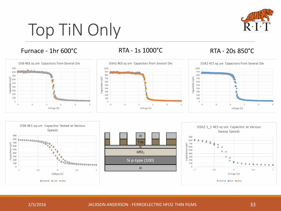
Top TiN Only
2/5/2016 JACKSON ANDERSON - FERROELECTRIC HFO2 THIN FILMS 33
Furnace - 1hr 600°C
RTA - 1s 1000°C
RTA - 20s 850°C

Top and Bottom TiN
2/5/2016 JACKSON ANDERSON - FERROELECTRIC HFO2 THIN FILMS 34
Furnace - 1hr 600°C
RTA - 1s 1000°C
RTA - 20s 850°C


