
FABRICATION AND PROPERTIES OF NANOSCALE MULTIFERROIC
HETEROSTRUCTURES FOR APPLICATION IN
MAGNETO-ELECTRIC RANDOM ACCESS MEMORY (MERAM) DEVICES
by
GUNWOO KIM
ARUNAVA GUPTA, COMMITTEE CHAIR
ROBERT W. SCHARSTEIN
JEFF JACKSON
SUSHMA KOTRU
GREGORY B. THOMPSON
A DISSERTATION
Submitted in partial fulfillment of the requirements
for the degree of Doctor of Philosophy
in the Department of Electrical and Computer Engineering
in the Graduate School of
The University of Alabama
TUSCALOOSA, ALABAMA
2012

Copyright Gunwoo Kim 2012
ALL RIGHTS RESERVED

ii
ABSTRACT
Magnetoelectric random access memory (MERAM) has emerged as a promising new
class of non-volatile solid-state memory device. It offers nondestructive reading along with low
power consumption during the write operation. A common implementation of MERAM involves
use of multiferroic tunneling junctions (MFTJs), which besides offering non-volatility are both
electrically and magnetically tunable. Fundamentally, a MFTJ consists of a heterostructure of an
ultrathin multiferroic or ferroelectric material as the active tunneling barrier sandwiched between
ferromagnetic electrodes. Thereby, the MFTJ exhibits both tunnel electroresistance (TER) and
tunnel magnetoresistance (TMR) effects with application of an electric and magnetic field,
respectively.
In this thesis work, we have developed two-dimensional (2D) thin-film multiferroic
heterostructure METJ prototypes consisting of ultrathin ferroelectric BaTiO3 (BTO) layer and a
conducting ferromagnetic La0.67Sr0.33MnO3 (LSMO) electrode. The heteroepitaxial films are
grown using the pulsed laser deposition (PLD) technique. This oxide heterostructure offers the
opportunity to study the nano-scale details of the tunnel electroresistance (TER) effect using
scanning probe microscopy techniques. We performed the measurements using the MFP-3D
(Asylum Research) scanning probe microscope. The ultrathin BTO films (1.2 – 2.0 nm) grown
on LSMO electrodes display both ferro- and piezo-electric properties and exhibit large tunnel
resistance effect.
We have explored the growth and properties of one-dimensional (1D) heterostructures,

iii
referred to as multiferoric nanowire (NW) heterostructures. The ferromagnetic/ferroelectric
composite heterostructures are grown as sheath layers using PLD on lattice-matched template
NWs, e.g. MgO, that are deposited by chemical vapor deposition utilizing the vapor-liquid-solid
(VLS) mechanism. The one-dimensional geometry can substantially overcome the clamping
effect of the substrate present in two-dimensional structures because of the reduced volume of
the template. This leads to minimum constraint of displacements at the interface and thereby
significantly enhances the magnetoelectric (ME) effect. We characterized the nanostructures
using scanning electron microscopy (SEM) and transmission electron microscopy (TEM).
The results of our studies utilizing multiferroic 2-D thin films and 1-D NW architectures
clearly demonstrate the potential of these heterostructures for future device applications, such as
in MERAM, data storage, magneto-electric field sensors, etc.

iv
DEDICATION
SCRIPTURE
His Strength
Isaiah 41:10
So do not fear, for I am with you,
do not be dismayed, for I am your God.
I will strengthen you and help you,
I will uphold you with my righteous right hand.

v
LIST OF ABBREVIATIONS AND SYMBOLS
Rp Parallel magnetization
Rap Antiparallel magnetization
Magnetic susceptibility
TC Curie Temperature
TN Neel Temperature
K Kelvin Temperature
Magnetic induction
Magnetic field
Electric field
Mr Remanent magnetic polarization
Pr Remanent electric polarization
MS Saturation magnetic moment
E Magnetoelectric voltage coefficient
f.u Formula unit
µC micro Coulomb
Psi angle ranging from 0o to 90
o
Phi angle ranging from 0o to 360
o
Wavelength of X-ray (Equal to 1.5405 Å for Cu K X-ray)

vi
B Bohr magneton (Equal to 0.92710-20
erg/Oe)
Torr Non-Si unit of pressure (760 Torr = 1 atmosphere)

vii
ACKNOWLEDGMENTS
I am heartily thankful to my advisor, Professor Arunava Gupta, whose wisdom,
supervision and support from the preliminary to the concluding level enabled me to develop an
understanding of the research subjects. When I experienced a serious medical issue, he had kept
in touch with me and given me an opportunity to continue pursuing my Ph.D program. Without
his encouragement, I would not have been able to complete my degree. I am sincerely grateful to
my co-advisor Professor Robert W. Scharstein, for his guidance throughout my dissertation
writing. I am truly thankful to my committee members, Professor Jackson, Professor Kotru and
Professor Thompson. They truly prayed for my recovery and guided me to complete my degree
with their invaluable support and input. I sincerely thank Professor Subhadra Gupta for her warm
heartedness. I am also thankful to Professor Haskew for his prayers for my recovery. I am
especially thankful to Professor Bruce Kim. He offered me an opportunity to seek the Ph.D
degree program at The University of Alabama.
I would like to thank former and present group members; Dr. Prahallad Padhan, Dr.
Dipanjan Mazumdar, Dr. Vilas Shelke, Dr. Ningzhong Bao, Dr Liming Zhen, Dr. Krishna Chetry,
Dr. Yu-Hsiang A. Wang, Neha Pachauri and Mehmet Yurtişigi who gave me valuable help and
support for my research. I am obliged to the staff at the Center for Materials for Information
Technology (MINT). They gave me their endless support, love and prayers.

viii
I also thank church members in Korean Presbyterian Church at Tuscaloosa. They stayed
overnight with me at the hospital and prayed for my recovery.
I would also specially thank Professor Lee, Kyoo-Hyung at the Asan medical center in
Korea. Without his medical care, I could not complete this degree program and even not able to
be alive.
I am truly thankful to my parents for their endless love and care. My mother, KyungHa
Kim, donated her bone marrow to her son and gave me life twice. My father, WonSik Kim, made
many sacrifices to save his son.
Finally, I am truly and heartily thankful to my wife, Gimin Nam. Without the support of
Gimin, I could not have survived and this work would never have been possible. She never
stopped her sacrifice and encouraging me to persist. I love Gimin so much. I will be truly forever
thankful to you. I am also thankful to my daughter, Christine Chae-Min Kim. She grew up
without my support for a few years but she became a great child. I love you, Chae-Min.
Lastly, I thank God. He never gave me up when I had walked through the darkest valley
and showed me His love through my salvation.
ix
CONTENTS
ABSTRACT ................................................................................................ ii
DEDICATION ........................................................................................... iv
LIST OF ABBREVIATIONS AND SYMBOLS ........................................v
ACKNOWLEDGMENTS ........................................................................ vii
LIST OF TABLES .................................................................................... xii
LIST OF FIGURES ................................................................................. xiii
1. INTRODUCTION ...................................................................................1
2. LITERATURE REVIEW ........................................................................7
2.1 Memory devices ................................................................................7
2.1.1 Ferroelectric memory ...................................................................7
2.1.2 Ferromagnetic memory ..............................................................10
2.1.3 Magneto-Electric Random Access Memory (MERAM) ...........13
2.2 Multiferroic compositions ...............................................................16
2.3 Multiferroic nanowires ....................................................................21
3. FABRICATION AND CHARACTERIZATION TECHNIQUES AND
REVIW OF SELECTED MATERIALS ................................................23
3.1 Fabrications .....................................................................................23
3.1.1 Pulsed laser Deposition (PLD) ..................................................23
3.1.2 Chemical Vapor Deposition (CVD) ..........................................24
3.1.3 Electron beam (E-beam) lithography ......................................26

x
3.2 Characterizations .............................................................................28
3.2.1 X-ray diffraction (XRD) ............................................................28
3.2.2 Transmission electron microscopy (TEM) ................................30
3.2.3 Piezoresponse force microscopy (PFM) ..................................32
3.2.4 Conducting atomic force microscopy (C-AFM) .......................33
3.2.5 Other characterization methods .................................................35
3.3 Review of selected materials ..........................................................36
3.3.1 Barium titanate (BaTiO3, BTO) ................................................36
3.3.2 Nickel ferrite (NiFe2O4, NFO) ................................................37
3.3.3 Lanthanum strontium manganite (LaSrMnO3, LSMO) ............39
4. MAGNESIUM OXIDE (MgO) and MULTIFERROIC NANOWIRES
(NWs) .........................................................................................................40
4.1 Introduction .....................................................................................40
4.2 Random arrangement of NWs on MgO and Si substrates ...............41
4.2.1 Morphologies .............................................................................41
4.2.2 Histograms of MgO NWs and gold nanoparticles ....................45
4.3 Systematic pattern array of MgO NW on MgO substrate ...............47
4.3.1 Square cross-section pattern ......................................................47
4.3.2 Single dot pattern .......................................................................49
4.4 Multiferroic nanowires ....................................................................53
4.4.1 Thin BaTiO3 and NiFe2O4 films ................................................55
4.4.2 Single phase BaTiO3 or NiFe2O4 coated NWs ..........................58
4.5 Summary .........................................................................................63

xi
5. NANOSCALE ELECTRORESISTANCE PROPERTIES OF ALL-
OXIDE MAGNETO-ELECTRIC TUNNEL JUNCTION WITH ULTRA-
THIN BARIUM TITANATE BARRIER . ................................................64
5.1 Introduction .....................................................................................64
5.2 Experimental results and discussion ................................................67
5.2.1 Piezoelectric properties of the ultrathin BaTiO3 films...............67
5.2.2 Conductive properties of the ultrathin BaTiO3 films .................71
5.3 Summary .........................................................................................79
6. CONCLUSION AND FUTURE WORK .............................................80
7. REFERENCES ......................................................................................83
BIBLIOGRAPHY ......................................................................................89
APPENDIX A ............................................................................................ 90

xii
LIST OF TABLES
2.2.1 Multiferroic compositions .................................................................20
4.3.1 Tabulation of the absolute number and density of the grown
nanowires at different patterned area, along with the number of gold
catalyst particles formed at the growth temperature. (Reproduced with
permission from ref. [81]) ..........................................................................51
4.4.1 Lattice parameter (a) and lattice mismatches (%) for each material.53
5.1.1 Comparison of properties of three different conductive tips. ...........66
5.2.1 Theoretical values calculated by Brinkman equation fit using three
different conductive tips. ...........................................................................78

xiii
LIST OF FIGURES
2.1 (a) Perovskite structure of BaTiO3 where a small cation (O) at the
center of an octahedron of oxygen anions with large cations (Ba) at the
unit cell corners, and (Ti4+
) metal ions placed at a center of the unit cell.
(b) and (c) illustration of a transition phase after Ti4+
movements,
Up/Down. Typical hysteresis loop is shown between (b) and (c)
(Adapted from ref. [3]). ...............................................................................8
2.2 Schematic of the principle concept of ferroelectric tunnel junction
(FTJ) and three fundamental mechanisms (a-c) that can lead to electric
tunnel resistance. (Reproduced with permission from ref. [32]) .................9
2.3 Schematic illustration of density of states in different metal oxide
materials. 3d and 4s densities in first-row transition metals and electron
spin up and down densities of states. The horizontal lines indicate the
Fermi levels in ferrite materials, Zn, Cu, Ni, Co, Fe, and Mn. (Adapted
from ref. [37]) ............................................................................................11
2.4 Schematic illustrating principle of magnetoresistance (MR) due to the
combination of electro spins. (a) Low resistance state with parallel spins
direction of the two ferromagnetic layers. (b) High resistance state with
anti-parallel spins direction of the two ferromagnetic layers... ..................12
2.5 Two fundamental layer structures to configure MERAM. (a) Single FE
layer is sandwiched by two FM layers. (b) Two FM layers are separated
by a single-phase multiferroic with combined properties of ferroelectricity
(FE) and ferromagnetism (FM)/antiferromagnetism (AFM). ....................14
2.6 Schematic of the layer structures of MERAM. (a) Two ferromagnetic
layers (blue color) are aligned. Low or high resistance state owing to the
magnetization configuration (parallel or antiparallel) of the ferromagnetic
layers. (b) A bottom ferromagnetic layer is on the multiferroic layer. If
magnetoelectric coupling (MEH) is strong enough by the ferroelectric
polarization in the multiferroic layer the electron spins rotates to reset the
magnetization configuration change of the bottom ferromagnetic layer,
resulting parallel to antiparallel combination of the two ferromagnetic
electrodes (Reproduced with permission from ref. [13]). ..........................16

xiv
3.1.1 Schematic of a PLD system used in this study. It consists of a high
vacuum-high vessel combined with a load lock and process chamber, a
circular disk for rotating multiple targets, a load arm to insert a substrate
into the process chamber, heating elements, gas delivery ports, optical lens
and quartz window to guide Excimer laser beam into the process chamber.24
3.1.2 Schematic of a typical CVD system for synthesizing nanowires
(NWs). It consists of a quartz reaction tube, a furnace to provide required
high temperature, gas inlet/outlet ports, precursor source and a substrate
where NWs are grown. ..............................................................................25
3.1.3 Schematic diagram illustrating the growth sequence of MgO
nanowires. The square gold regions are patterned using e-beam
lithography. Gold nanoparticles are formed within the square region at a
critical annealing temperature (925oC). Single free-standing MgO NWs
are grown on the substrate with the gold particles being lifted up.
Reproduced with permission from ref. [81]) ............................................26
3.1.4 Schematic illustrating the process of E-beam Lithography. Two
kinds of patterning processes are described depending on properties of
resists, positive and negative films as shown in case (I) and (II). As an
initial preparation, E-beam resist is spin coated on silicon wafer as shown
in the middle figure. (a) E-beam penetrates through the pattern mask. (b)
Exposed resist changes chemical structure to become more soluble in the
developer. (c) After developing, exposed region is removed in the case of
positive resist and retained in the case of negative resist. (d) Thin gold film
is deposited using e-beam evaporator. (e) After stripping to remove
unexposed resist, final patterns with gold thin film remains. ....................27
3.2.1 Schematic diagram illustrating Bragg's law, where n is an integer,
is the wavelength of X-ray, d is the lattice spacing, and is the diffraction
angle. ..........................................................................................................28
3.2.2 Theoretical method to determine the film thickness using X-ray
reflectivity (XRR) technique. (a) Oscillation curves (b) Symbols indicate
the calculated data points using Eq. (2). Linear fit is applied to determine
the value of slope, providing the film thickness ........................................29
3.2.3 Schematic providing a view of tilt and rotation angles for pole figure
measurement. Here tilt, psi () ranges from 0o to 90
o, and rotation phi (),
ranges from 0o to 360
o. is an incident angle of X-ray beam with respect
to substrate surface .....................................................................................30
3.2.4 Schematic of the TEM image modes. (a) Bright-field image mode,
(b) Dark-field image mode. (Adapted from ref. [72]) ...............................32

xv
3.2.5 Schematic of typical PFM measurement system. The phase
deformation of a sample is occurred by biased initial tip scans. Then the
AFM tip (dashed and solid) indicates the electromechanical displacement
while scanning over the surface and visualizes the phase image through
imaging processes. .....................................................................................33
3.2.6 Schematic diagram for conducting AFM measurement. A conductive
tip senses the different conductivity and detects current while scanning the
surface of a sample.....................................................................................34
3.2.7 Schematic of the basic configuration of a RHEED system. An
incident electron beam at a shallow angle is diffracted from the sample
surface and projects diffraction patterns on the screen. A sample is placed
in an ultrahigh vacuum vessel and can be rotated 360 degrees, leading to
various diffraction patterns owing to different crystal orientations. ..........36
3.3.1 Schematic of BaTiO3 (BTO) crystal structure. The BTO material is
deformed from cubic to tetragonal structure by an application of an
applied electric field at room temperature. ................................................37
3.3.2 Schematic of inverse spinel NiFe2O4 structure consisting of
tetrahedral A sites and octahedral B sites. The cubic structure is
configured by combining these two sites in a FCC oxygen lattice.
(Adapted from ref. [37]). ...........................................................................38
4.2.1 (a) SEM images showing the growth of vertically aligned MgO
nanowires on a (001)-oriented MgO substrate. The inset shows an image
of the gold particles formed by heating the gold film on the MgO substrate
to the growth temperature and then cooled down without actual growth of
the nanowires. (b) SEM image showing MgO nanowires grown on a
(001)-oriented Si substrate for a total deposition period of 60 minutes. The
wires grow in random directions exhibiting a basket-weave-like
morphology. The inset shows the gold particles formed by heating the
gold film on the Si substrate to the growth temperature and then cooled
down without actual growth of the nanowires. The marker for both inset
images is 100 nm. (Reproduced with permission from ref. [81] ...............43
4.2.2 (a) TEM diffraction pattern and bright field image of a single MgO
nanowire grown on the MgO substrate indicating (001) growth direction.
(b) MgO nanowire showing a cubic-rod shape morphology; the image to
the right has the cube edges highlighted. (c) TEM bright field image of a
MgO nanowire with the gold catalyst on top, which has been grown on an
MgO substrate. (d) TEM bright field image of MgO nanowires grown on
Si substrate. Note the rectangular shape of the nanowires and
interconnection of the wires to each other in different directions. This type
of interconnection is not evident in the MgO nanowires grown on the

xvi
MgO substrate. (Reproduced with permission from ref. [81]) ..................44
4.2.3 Histograms comparing the diameter of MgO nanowire grown on (a)
MgO (001) and (b) Si (001) substrates. (Reproduced with permission from
ref. [81]) .....................................................................................................46
4.2.4 Histograms comparing the size of gold nanoparticles formed using a
1 nm thick gold film on (a) MgO (001) and (b) Si (001) substrates.
(Reproduced with permission from ref. [81]) ............................................48
4.3.1 SEM images showing different patterned regions of the MgO
nanowires. The bright spot on the top of each nanowire is the gold catalyst
particle. [(a) and (d)] 0.25m2, [(b) and (e)] 1m
2, and [(c) and (f)] 4m
2.
A blanket gold film of 1 nm thickness is deposited and patterned using e-
beam lithography for the selective growth of the nanowires. (Reproduced
with permission from ref. [81]) ..................................................................50
4.3.2 Histogram of the size distribution of gold nanoparticles formed
within the 1m2 patterned regions on an MgO (001) substrate. The
average nanoparticle size is 20 nm. (Reproduced with permission from ref.
[81])............................................................................................................51
4.3.3 SEM images of a single MgO NW (a) Gold dot pattern in 10 x10
arrays. The diameter of dots is approximately 200 nm. (b) Single MgO
NW grown within each dot array. The height is around 5-10m. .............52
4.4.1 Schematic of multiferroic nanowire. (a) Template MgO NWs
produced by VLS growth mechanism in a typical CVD process. NWs are
vertically oriented. (b)-(c) „core-shell‟ type multiferroic nanowire
consisting of ferrite (yellow)-ferroelectric (purple) thin film deposited on
the template post of MgO NW by PLD technique. (d) Cross section view
of the muliferroic nanowire .......................................................................54
4.4.2 (a) -2 X-ray diffraction spectra for a single-phase NFO and BTO
film on MgO substrate. Peaks are close to the angular positions of the
(004) and the (002) reflection of NFO and BTO. (b)-(c) Rocking curves
for NFO and BTO films. The vertical solid lines indicate the bulk NFO
and BTO 2 peak positions. Here, makers, *, , and , indicate MgO bulk
peak, NFO and BTO film peaks. ..............................................................55
4.4.3 Phi scans of (311) reflection of bilayers of NFO and BTO films on
MgO. Four symmetric peaks spaced 90 degrees apart are observed. ........56
4.4.4 RHEED patterns along [100] for epitaxial growth of BTO and NFO
thin films on (100)-oriented MgO substrate. (a) RHEED image of MgO
substrate prior to deposition. (b)-(c) RHEED image of BTO and NFO

xvii
films. ..........................................................................................................57
4.4.5 SEM images of nanowires. (a) Template MgO NWs. Gold balls
lifted up and positioned on top of MgO NWs during a growth. (b) Single-
phase BTO NWs. (c) Single-phase NFO NWs. .........................................59
4.4.6 TEM images of BaTiO3 NWs. (a) Bright field TEM image showing
single-BTO NW. Insert image shows a diffraction pattern, indicating well
crystallized structure. (b) BTO NW has a cubic structure and <001>
growth direction same as the template MgO. (c) HRTEM images
displaying lattice spacing at the boundary of MgO and BTO layers. (d)
EDS analysis indicates presence of Ba, Ti, Mg, and O. ...........................60
4.4.7 TEM images of NiFe2O4 NWs. (a) Bright field TEM image showing
single-NFO NW. Insert image shows a diffraction pattern, indicating well
crystallized structure. (b) NFO NW has a cubic structure and <001>
growth direction, same as the template MgO. (c) HRTEM image
displaying lattice spacing of MgO and NFO layers. The lattice spacing‟s
cannot be resolved because MgO and NFO are isostructural with very
similar lattice parameters. (d) EDS analysis indicates presence of Ni, Fe,
Mg, and O. .................................................................................................62
5.2.1 AFM surface topology image of BTO film of thickness 2 nm. RMS
roughness of the film is 0.2 nm. .................................................................68
5.2.2 Schematic for generating polarization pattern (a) and a polarized
image showing UA logo with an elephant (b). Black color zone is written
using a tip voltage, Vtip = - 3V and white color is zone is written using a
tip voltage, Vtip = + 3V. .............................................................................69
5.2.3 Hysteresis loop corresponding to polarization switching of BTO
film. (a) Phase map in degree and (b) amplitude map exhibiting a butterfly
loop. ...........................................................................................................70
5.2.4 Schematic illustration for creating different polarization state
regions. (a-1) 2m × 2m square zone poled by a negative voltage. (a-2) 1
m × 1m center region poled by a positive voltage. (a-3) is re-poled area
by a positive voltage after 6 hours. (b) PFM image after initial polarization
resulting from steps (a-1) and (a-2). (c) Re-read PFM image after step (a-
3). ...............................................................................................................71
5.2.5 Schematic of configurations for polarization orientation. (a)
Polarization pointing upward by application of a positive sample bias. (b)
Current map while scanning the region. (c) Polarization pointing
downward by application of a negative sample bias. (d) Current map while
scanning the same region. For the measurements the tip is grounded and

xviii
the current is measured using an amplifier. ...............................................73
5.2.6 I-V curves measured with different polarization states, upward or
downward, corresponding to switch ON or OFF state. The black lines
represent I-V curves fits using the Brinkman model. Insert shows the TER
and ON/OFF ratio. .....................................................................................74
5.2.7 I-V curves and TER values measured by DPER 18 (a)-(b), and PtSi
(c)-(d) commercial tips at different polarization states, upward or
downward, corresponding to switch ON or OFF state. .........................76
5.2.8 Comparison of barrier heights of polarization ON and OFF states
due to applied different commercial tips. ..................................................78
Appendix A1 SEM images of four point contact pads fabricated by using
E-beam lithography. (a) First designed pads where four legs are clearly
patterned. (b) Secondly designed pads where single NW is successfully
placed on the four legs. ..............................................................................91

1
CHAPTER 1
INTRODUCTION
Ferroelectric and ferromagnetic oxide materials have been used in a wide range of
applications such as sensors, transducers, microwave components, and data storage [1, 2].
Among these applications, ferroelectric random access memory (FRAM) [3] and magnetic
random access memory (MRAM) [4] have received a great deal of attention as an alternative to
traditional semiconductor-based memory (RAM). These types of memory are capable of non-
volatility arising from spontaneous and switchable polarization or magnetization. FRAM offers
fast access speed (~5 ns) and lower power consumption, while MRAM has very good data access
speed and endurance. As a tradeoff, data destruction in the readout process is a drawback for
FRAM because of the displacement current, and writing energy for magnetization switching is a
handicap of MRAM [5]. These weaknesses ultimately limit the performance of the memory
devices. Therefore, a new type of the memory device is required to provide nondestructive
reading and low power consumption in write operations. Multiferroic memory has recently
emerged as a potential device because it meets these requirements.
The term “multiferroic” was first used by H. Schmid in 1994 to denote the exhibition of
two or more ferroic order parameters, which are ferroelectricity, ferromagnetism, and
ferroelasticity in the same phase [6]. A multiferroic material was originally discovered by
Röntgen [7], who reported that a moving dielectric became magnetized when placed in an
electric field and reverse-polarized in a magnetic field. Debye called this phenomenon the
magnetoelectric (ME) effect [8, 9].

2
The ME effect is achieved by the combination of two different control mechanisms as
represented in the symbolic relationships [10]
.
In MEE, magnetization is controlled by the electric field [11]; when an electric field is applied to
a multiferroic composite, the piezoelectric phase changes its direction of electrical polarization
resulting in mechanical deformation. It is then transferred to the magnetic phase, producing
magnetization. In MEH, it is the reversed effect; electric polarization results from a magnetic
field [12].
Multiferroic random access memory (MERAM) using the MEE control method has been
proposed [13] as a novel technique for the practical application of ME effect. This type of
memory operates via the combination of electromagnetic polarization and tunneling at an
interface between a ferroelectric and ferromagnetic/anti-ferromagnetic film, which provide a
multiferroic composite. The memory device writes and reads information bits by using the
combination of ferroelectric tunnel junction (FTJ) and magnetic tunnel junction (MTJ) [14],
respectively. The FTJ provides low power consumption and high data access speed and MTJ
offers nondestructive reading operations in spintronics [15]. Spintronics exploits the
phenomenon of magnetoresistance (MR) [16] rather than magnetic induction ( ) for spin
rotations owing to scaling down in device areas.
Although MERAM promises a new route to memory devices, practical fabrication of the
device remains at an early stage because of technical obstacles. The development of ultrathin
3
ferroic tunnel barriers, which have stable and switchable polarization for writing information bits
at room temperature, is especially challenging because of the disappearance of the ferroic
properties below a critical thickness [17]. A few groups have reported that ultrathin ferroelectric
films act as tunnel barriers as a key configuration of ferroelectric tunnel junctions (FTJ) in a
small number of unit cells [18, 19, 20].
Fabricating multiferroic composites in one dimension (1-D) geometry, which makes it
possible to scale down to nanometer size device, presents another challenging obstacle. The
geometry may resolve a drawback of two-dimensional (2-D) geometry, which has a large in-
plane constraint on clamping condition at the substrate, resulting in poor ME response [21]. It is
necessary to configure the low dimensional multiferroic using nano materials such as
nanowires/tubes in order to pursue the alternative geometry, but these structures have not yet
been realized because of their complexity and technical difficulty in preparation. These
challenges require better methods of state-of-the-art multiferroic architecture for new memory
devices or other multifunctional applications characterized by the unique properties of
multiferroics.
This study has two major objectives. First, we studied a low dimensional multiferroic,
which is also referred to as one-dimensional (1-D) heterostructure multiferroic nanowire. This
type of geometry would overcome the clamping condition exhibited in 2-D geometry because a
reduced volume is expected, leading to minimum constraint at the interface of the films and
substrate. Initially, we were strongly motivated by a report of Petrov et al. [22], who presented a
theoretical model comparing the ME voltage coefficient for three different geometries: 2-D thin
film, nanopillar, and nanowire (NW). They found that a NW structure displays a higher ME
voltage coefficient than 2-D thin films because of the reduced volume of the 1-D template
4
substrate, minimizing the surface-clamping effect at the interface. The NW structures acting
primarily as low dimensional elements have gained much attention because of their unique
properties. Flexibility and preferable geometry give rise to nano scale devices, logic circuits, and
bio-chemical (or medical) sensors [23, 24]. Functional NWs consisting of ferroelectric or ferrite
material have also attracted interest because of the polarization/magnetization behavior that
offers switchable device applications in memory and sensors controlled by electric and/or
magnetic fields [25]. For these reasons, one-dimensional multiferroic NW structures offer
opportunities to explore a wide range of applications in nano science.
Secondly, by taking advantage of coupled multiferroic layer architecture [26], which
relaxes the composition limitations of material selection by combining ferroelectric/piezoelectric
and ferromagnetic materials with a large magnetostriction, we developed coupled multiferroic
composites composed of barium titanate (BaTiO3, BTO) and lanthanum manganese ferrite
(La0.67Sr0.33MnO3, LSMO). These coupled multiferroic composites enabled us to study magneto-
electric tunnel junctions (METJ), [27] combined tunneling magnetoresistance and tunnel
electroresistance (TMR-TER). The principal idea comes from tunnel resistance, which is
configured in a ferromagnetism (FM)/spacer/ferromagnetism (FM) sandwich structure. Two FM
films separated by a spacer layer can lead to magnetoresistance (MR) effect because of a
resistance difference between parallel and antiparallel configuration of magnetization. The
spacer is an insulator material that serves as a barrier layer. In this study, we selected a BTO
ultrathin film because it is widely used as a ferroelectric and piezoelectric material and is a good
candidate as a junction barrier, consistent with the principle of ferroelectric tunnel junction (FTJ).
We characterized the ultrathin BTO films using scanning probe microscopy to investigate the
property of the tunnel barrier and characterize the ferroelectric and piezoelectric properties.

5
Based on the results of these characterizations, we propose that a novel oxide multiferroic
ultrathin film of BTO deposited on ferromagnetic LSMO will be suitable to design novel
prototype devices for a wide range of applications, including MERAM, data storage, and
magneto-electric field sensors.
To pursue these two objectives, we combined chemical vapor deposition (CVD) and
pulsed laser deposition (PLD) techniques to synthesize magnesium oxide (MgO) nanowires as
template posts and deposit sheath layers, coupling ferroic thin films onto the nanowires in a core-
shell structure [28] to form 1-D structure configuration. Methods of characterization included
microscopic images, crystallinity, and histogram of nanowires using scanning electron
microscopy (SEM) and transmission electron microscopy (TEM). Based on these results, we
propose that the synthesis method is applicable for forming multiferroic nanowires
heterostructures.
We designed four-point contact pads using electron beam (e-beam) lithography and
placed a single nanowire onto this structure, allowing the measurement of current (resistance)
changes of single multiferroic nanowire as a function of externally applied magnetic field. The
detail is described in an appendix.
We also used the PLD technique to grow bilayers of ultrathin films, which were then
characterized in terms of their crystallinity. Local ferroelectric properties were studied using
piezoresponse force microscopy (PFM) and conducting atomic force microscopy (C-AFM) for
phase deformation and current-voltage (I-V) characteristics of ultrathin ferroelectric films.
This dissertation is divided into six sections including this introductory chapter. Chapter
2 contains a literature review of the physical and engineering aspects of ferroelectric,
ferromagnetic, and multiferroic memory as well as a theoretical model for multiferroic

6
nanowires as the motivation of this study. Chapter 3 is a detailed technical review of fabrication
and characterization methods and reviews of selected materials used in this work. Chapter 4
describes the synthesis of template MgO nanowires, BaTiO3 or NiFe2O4 film-coated nanowires
as an intermediate step toward multiferroic nanowires. Chapter 5 describes multiferroic ultrathin
films of BaTiO3 deposited heteroepitaxially on LaSrMnO3 to form ferroelectric tunnel junctions
(FTJ) and investigation of the tunneling properties. Finally, Chapter 6 concludes with suggested
future work along with recommendations for the applications of the developed devices for
memory and storage.

7
CHAPTER 2
LITERATURE REVIEW
2.1 Memory Devices
2.1.1 Ferroelectric memory
Ferroelectric oxide materials exhibit switchable and spontaneous polarization reversal by
an applied electric field, piezoelectric behavior involving conversion of mechanical energy to
electric energy, and large static dielectric permeability. These unique material properties make
the ferroelectric oxide materials attractive for a wide range of device applications such as data
storage, electromechanical transducers like piezoelectric actuators and capacitors [29].
Ferroelectric random access memory (FRAM) is one of the well-known devices offering non-
volatile memory. In addition to non-volatility, the memory offers in recent technology
generations fast access time (5 ns) and lower power consumption and competes with traditional
semiconductor random access memory (RAM).
Some oxides of the perovskite family of compounds can be electrically polarized and are
ferroelectric, retaining the polarization when the electric field is removed. When an external
electric field is applied across the structure, there is a phase transition from cubic to tetragonal
crystal orientation by physical displacement of a transition metal ion up or down in the unit cell
along the field axis direction, resulting in non-centrosymmetry of the perovskite structure. A
spontaneous polarization is then derived largely due to the dipole moment arising from the shift.
Fig. 2.1 illustrates the structural distortion by the movement of a transition metal ion (Ti4+
) in
case of BaTiO3 and a hysteresis loop corresponding to the phase changes.

8
Figure 2.1 Perovskite structure of BaTiO3 where a small cation (O) at the center of an octahedron
of oxygen anions with large cations (Ba) at the unit cell corners, and (Ti4+
) metal ions placed at a
center of the unit cell. (b) and (c) illustration of a transition phase after Ti4+
movements,
Up/Down. Typical hysteresis loop is shown between (b) and (c) (Adapted from ref. [3]).
As described in Fig. 2.1, this polarization behavior makes the FRAM attractive as non-volatility
memory.
A ferroelectric tunnel junction (FTJ) utilizes a very thin ferroelectric layer as an active
barrier (spacer). In a FTJ, electrons are transported across the insulating ferroelectric barrier from
one conductive electrode to another by quantum mechanical tunneling [19]. The concept was
first proposed by Frenkel in 1930 [30] and its practical applicability was discussed by Esaki later
in 1971 [31]. Fig. 2.2 depicts a schematic of a ferroelectric tunnel junction [32]. As illustrated in
Fig. 2.2(a), because of incomplete screening at the ferroelectric barrier-electrode interface,
polarization reversal of the barrier may have an effect on the conductance of FTJ, resulting in

9
tunneling electroresistance (TER) effect (ref. [32]). In addition, two effects can contribute to the
tunnel current: a microscopic interface effect because of the shifting transition metal ion and
strain resulting from piezoelectric effect, as seen Fig. 2.2(b) and (c), respectively.
In order to achieve the tunneling phenomena, the tunnel barrier should be an ultrathin
film; otherwise electrons will not pass through the barrier because of exponentially decreasing
tunneling probability with thickness and also scattering effects. Fabricating ultrathin ferroelectric
layers is challenging not only because of defect formation but also due to the intrinsic loss of
ferroelectric behavior below a critical thickness [33]. There are a few reports that take account of
the thickness limit in terms of number of unit cells, above which ferroelectric BaTiO3 or BiFeO3
ultrathin films display ferroelectric and piezoelectric properties [34, 35].
Figure 2.2 Schematic of the principle concept of ferroelectric tunnel junction (FTJ) and three
fundamental mechanisms (a-c) that can lead to electric tunnel resistance. (Reproduced with
permission from ref. [32]).

10
2.1.2 Ferromagnetic memory
Ferromagnetic oxide materials have been used in a broad range of magnetic-based data
storage media, such as recording tapes for audio/video, hard disk head/write drivers, etc., [36]
because of their unique properties such as spontaneous magnetization and ferromagnetic
behavior. To explain the magnetization and ferromagnetism, Curie-Weiss‟s law and Stoner band
theories generally use the phenomenon of the spin and orbital momentum of electrons developed
in quantum physics [37]. Curie-Weiss law states that magnetic susceptibility () at Curie
temperature is given by
, (1)
where TC is the Curie temperature related to a molecular field and C is the Curie constant. Below
the Curie temperature, the molecular field defined by a magnetic moment enables a substance to
be magnetized by a parallel alignment of electron spins to each other. On the other hand, Stoner
band theory describes electrons partially coupling 3d and 4s orbital and different band energies
required to reverse their state because of narrow (3d) or broad (4s) density of states at the Fermi
level, as illustrated in Fig. 2.3. These different densities of state effect the exchange interaction
for electrons, predicting easier spin reversal for the increased alignment of spins in 3d than in 4s
bands to be ferromagnetic.
The physical understanding of the spin motion of electrons provides the basis of
numerous innovations related to magnetic-based recording devices. Initially, write/read heads for
hard disks were operated using magnetic induction ( ). However, the induction field is too weak
to be used as a signal generator when the storage bit size became smaller. As an alternative,
magnetoresistance (MR) techniques were used to produce more sensitive read head component.

11
Figure 2.3 Schematic illustration of density of states in different metal oxide materials. 3d and 4s
densities in first-row transition metals and electron spin up and down densities of states. The
horizontal lines indicate the Fermi levels in ferrite materials, Zn, Cu, Ni, Co, Fe, and Mn.
(Adapted from ref. [37]).
The first read head using MR was fabricated by IBM in 1991, which was configured utilizing
anisotropic magnetoresistance (AMR), originally introduced by William Thomson in 1856. Since
IBM‟s introduction of MR heads in hard disk drives, the data density of recording media has
kept increasing each year. For instance, the data density in 1991 was 0.1Gbit/in2 and the density
in 2003 was 100Gbit/in2. Now, recording density of up to 1Tbit/in
2 is available [15]. The
discovery of the giant magnetoresistance (GMR) and tunneling magnetoresistance (TMR) in
place of AMR triggered this technical trend [38, 39]. The GRM is configured as a sandwich
structure where two ferromagnetic electrode layers are separated by a non-magnetic metallic
spacer layer. In GMR, the current flowing across the metallic layer varies depending on the
relative magnetic configuration of the two ferromagnetic layers because of spin-dependent
transport. Fig. 2.4 schematically illustrates resistive changes owing to spin alignment of the two
electrodes (Fig. 2.4 adopts the CPP (current perpendicular to the plane) GMR structure). If the
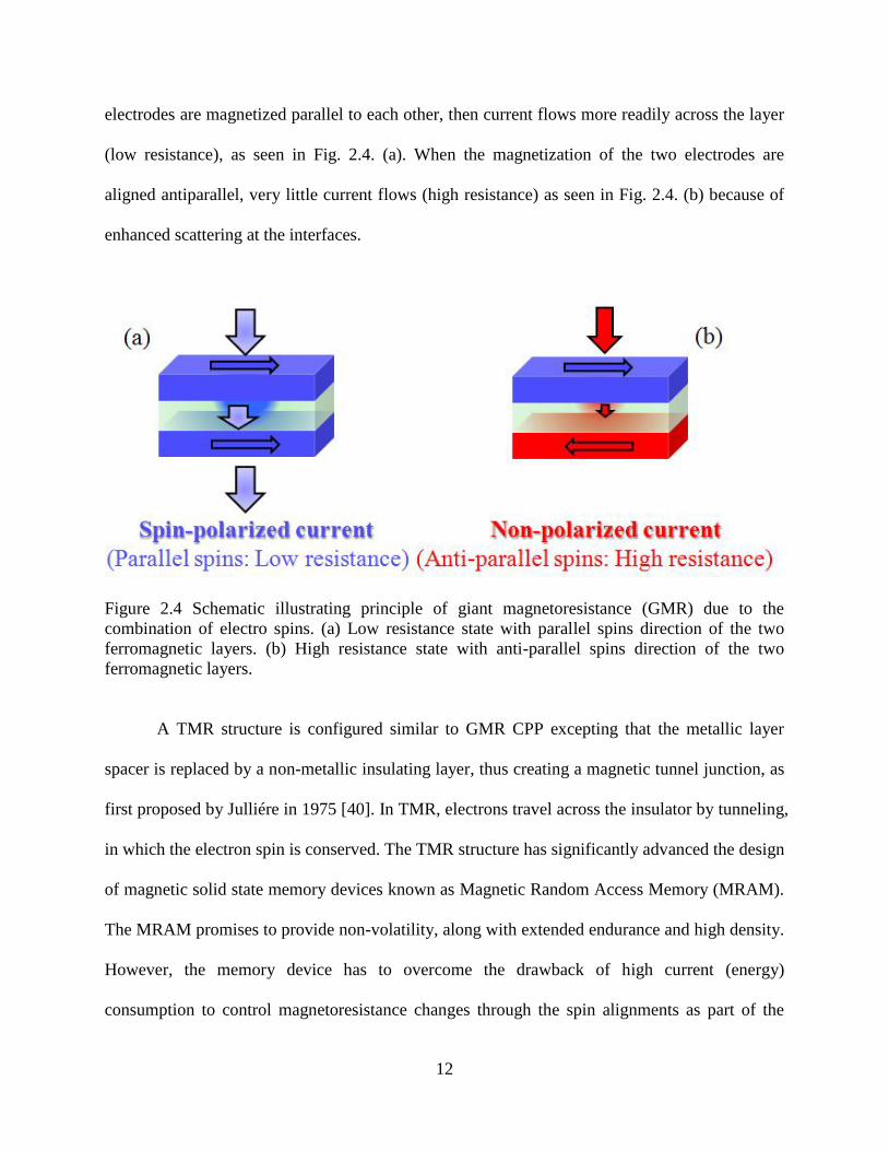
12
electrodes are magnetized parallel to each other, then current flows more readily across the layer
(low resistance), as seen in Fig. 2.4. (a). When the magnetization of the two electrodes are
aligned antiparallel, very little current flows (high resistance) as seen in Fig. 2.4. (b) because of
enhanced scattering at the interfaces.
Figure 2.4 Schematic illustrating principle of giant magnetoresistance (GMR) due to the
combination of electro spins. (a) Low resistance state with parallel spins direction of the two
ferromagnetic layers. (b) High resistance state with anti-parallel spins direction of the two
ferromagnetic layers.
A TMR structure is configured similar to GMR CPP excepting that the metallic layer
spacer is replaced by a non-metallic insulating layer, thus creating a magnetic tunnel junction, as
first proposed by Julliére in 1975 [40]. In TMR, electrons travel across the insulator by tunneling,
in which the electron spin is conserved. The TMR structure has significantly advanced the design
of magnetic solid state memory devices known as Magnetic Random Access Memory (MRAM).
The MRAM promises to provide non-volatility, along with extended endurance and high density.
However, the memory device has to overcome the drawback of high current (energy)
consumption to control magnetoresistance changes through the spin alignments as part of the

13
writing information of the bits. The drawback can be more critical when the device size is scaled
down to nanometer scale to achieve high data density because the large current, besides high-
energy consumption, can be the source of device heating and the destruction of information bits.
Therefore, it is a challenge to overcome this limitation.
2.1.3. Magneto-Electric Random Access Memory (MERAM)
Multiferroic memory, also referred to as magneto-electric random access memory
(MERAM), has emerged as an attractive candidate that provides nondestructive reading and low
power consumption in write operations [13]. Zhuravlev et al. first predicted the principle of
MERAM utilizing magneto-electric tunnel junctions (METJ) [27], which combines the tunnel
electroresistance (TER) and tunnel magnetoresistance (TMR) effects.
MERAM fundamentally consists of a sandwich layer structure as shown in Fig. 2.5. A
thin insulating active layer is sandwiched between two ferromagnetic (FM) electrodes. Here, two
types of sandwich layer can be chosen. One is a ferroelectric (FE) layer, as shown in Fig. 2.5(a),
and the other is a single-phase multiferroic layer with combined properties of ferroelectricity
(FE) and ferromagnetism (FM)/antiferromagnetism (AFM), as shown in Fig. 2.5(b). The layer
configuration leads to changes in the tunnel current by manipulation of the magnetization
parallel (Rp) or antiparallel (Rap) between the two ferromagnetic electrodes. Moreover, the
magnetization of the bottom ferromagnetic electrode can be electrically switched by changing
the polarization of the underlying FE layer (ref. chapter 1)
Fig. 2.6 depicts a schematic layer structure of possible MERAM device (ref [13]). First,
two ferromagnetic layers, top and bottom (blue color), are separated by a barrier. As expected in
the TMR effect, there is a low or high resistance state depending on the magnetization
configuration (or spin alignment) of the two ferromagnetic layers, parallel or antiparallel.

14
Figure 2.5 Two fundamental layer structures to configure MERAM. (a) Single FE layer is
sandwiched by two FM layers. (b) Two FM layers are separated by a single-phase multiferroic
with combined properties of ferroelectricity (FE) and ferromagnetism (FM)/antiferromagnetism
(AFM).
Secondly, the bottom ferromagnetic layer is positioned on a multiferroic FE/AFM layer. When
an electric field is applied across the multiferroic layer, the ferroelectric polarization is reversed.
If the magnetoelectric coupling (MEE) (electric control for magnetization response) is strong
enough by the reversed ferroelectric polarization field, electron spins rotate to reverse the spin
state at the interface of the AFM, causing a magnetization configuration change of the bottom
ferromagnetic electrode, with resulting parallel to antiparallel combination of the two
ferromagnetic electrodes. The change in magnetization configuration results in a resistance
change of the junction from low to high. Here, it is important to note that an electric field is used
to manipulate the relative spin alignment (parallel antiparallel) instead of a larger current, as
required in MRAM. This concept of “ferroelectric control of spin polarization” is thus attractive
for low energy switching of spintronic devices.
Another concept of ferroelectric control of tunneling was first demonstrated by Garcia et
al. in an experiment probing the spin polarization of electrons tunneling between metallic
electrodes through a thin ferroelectric BaTiO3 (BTO) tunnel barrier [41]. To demonstrate this

15
effect experimentally, they used half-metallic LaSrMnO3 (LSMO) bottom electrode as a spin
detector. Thereby the BTO/LSMO bilayer artificially provides a multiferroic tunnel junction
(MFTJ). They measured the TMR effect by manipulating the ferroelectric polarizations and TER
behavior through the BTO tunnel barrier at low temperature (4.2K).
The coexistence of TMR and TER effects in the MFTJ offers the potential of MERAM
device combined with MRAM and FRAM to read/write binary information. Furthermore, the
MERAM device offers a four-state resistance with the combination of two electric polarization
(P) and magnetization (M) states [42].
The key to the success of this type of device is the development of an ultrathin ferroic
film acting as the tunnel barrier that retains ferroelectric properties [17]. The recent discovery of
ferroelectric properties being retained in ultrathin ferroelectric layers has opened ways to explore
this novel layer architecture [43]. Indeed, a few groups have reported the development and
characterization of ultrathin ferroic films to demonstrate potential for magnetoelectric random
access memory devices [44].

16
Figure 2.6 Schematic of the layer structures of MERAM. (a) Two ferromagnetic layers (blue
color) are aligned. Low or high resistance state owing to the magnetization configuration
(parallel or antiparallel) of the ferromagnetic layers. (b) A bottom ferromagnetic layer is on the
multiferroic layer. If magnetoelectric coupling (MEE) is strong enough by the ferroelectric
polarization in the multiferroic layer the electron spins rotates to reset the magnetization
configuration change of the bottom ferromagnetic layer, resulting parallel to antiparallel
combination of the two ferromagnetic electrodes (Reproduced with permission from ref. [13]).
2.2 Multiferroic compositions
After discovery of the first multiferroic material nickel iodine boracite, Ni2B7O13I [45],
various bulk single-phase ceramic multiferroics have been extensively investigated in the 20th
century. In particular, perovskite-type RMnO3 oxides, where R is rare-earth materials like Y, Bi,
Ho, La, and Nd, Mn=manganites, have received much attention [46]. There are, for instance,
yttrium manganite YMnO3 (YMO) and bismuth Bi-based compounds such as BiMnO3 (BMO)
and BiFeO3 (BFO), which exhibit ferroelectrictiy and anti-ferromagnetism.

17
Such single-phase materials are, however, very limited. The critical issue is that a
limited number of single-phase compounds exist in nature because of the inconsistency of
coexistence of ferroelectricity requiring an insulator and ferromagnetism needing a non-d0
transition metal in the same phase at room temperature [47].
As alternative, Van Suchtelen [48] proposed the concept of a two-phase ceramic
composite in 1972 and predicted that the ME response of the material could result from elastic
coupling between the ferromagnetic and ferroelectric phases. Based on his theory, scientists in
Philips Laboratory synthesized the two-phase ceramic composite of BaTiO3-Ni(Co, Mn)Fe2O4
[49]. In the early 1990, other two-phase ceramic multiferroics using ceramic composites of
ferrites and Pb(ZrTi)O3 (PZT) were studied by typical sintering processes [50]. The experiments
motivated theoretical studies [51]. Both experimental and theoretical work encouraged scientists
to study various families of bulk two-phase ceramics. However, the two-phase ceramics still
have limitations for practical devices because of their drawbacks such as porosity, uncontrolled
dispersion or brittle and high eddy current loss at the interface, resulting in low ME effect.
From the last several years, various film techniques like pulsed laser deposition (PLD),
sputtering and molecular beam epitaxy (MBE) have been employed to synthesize multiferroic
films [52, 53, 54]. BiMnO3 (BMO), BiFeO3 (BFO), and YMnO3 (YMO) films were actively
studied [55, 56, 57]. Even though bulk film composites have received considerable attention,
there is a significant negative aspect, which is large strain in films because of the much thicker
substrate, resulting in a low ME coefficient.
Nanostructured thin films designed by a coupling of ferroelectric (FE) and ferromagnetic
(FM) layers have been introduced because the structure can offer more degrees of freedom such
as potential porosity, lattice strain and interlayer interaction which were drawbacks presented in

18
previous multiferroic compositions. As the first successful work, a vertical heterostructure was
experimentally reported in a structure of nanopillar geometry and proved theoretically later [58,
59]. The structure was synthesized by a self-assembly method involving magnetic spinel,
CoFe2O4 (CFO), implanted into a ferroelectric perovskite matrix, BaTiO3 (BTO), using pulsed
laser deposition. The vertical nanopillar structure displayed high remanent magnetic polarization
(Mr) close to 300emu/cm3 and low remanent electric polarization (Pr) of approximately
10C/cm2. However, the vertical structure showed a critical drawback, which is leakage through
the interfaces of the nanopillar matrix, leading to low resistance. The leakage problem ultimately
reduces ME effect, limiting device applications. Years later, a horizontal heterostructure was
experimentally and theoretically studied coupling bilayers with ferroelectric, BTO and
ferromagnetic, NiFe2O4 (NFO) or CFO, films [60]. The horizontal structure reduces the leakage
problem found in the vertical structure by being a ferroelectric layer acting as insulator to cut off
current flow. The structure however exhibits weak magnetoelectric (ME) effect because of
clamping condition owing to the large two-dimensional substrate thickness and lattice strain at
interface between films and substrate. Therefore, it is still challenging to resolve the weak ME
coefficient and the constraint.
As another coupled multiferroic, the combination of ferromagnetic (FM) and dual ferroic
order materials combined with ferroelectricity/antiferromagnetism (FE/AFM) has been
investigated. Lanthanum barium manganite (LaBaMnO3, LBMO) and yttrium manganite
(YMnO3, YMO) have been studied. However, there materials are not very attractive because of
the coexistence of the coupled ferroic properties only at low temperatures [16, 61], which is
undesirable for practical applications. As another choice, bismuth ferrite (BiFeO3, BFO) has

19
been extensively studied as a potential candidate because of the appearance of the binary ferroic
orders (AFM /FE) at room temperature [62].
These types of multiferroics have received great attention as emerging materials for use
in magneto-electro random access memory (MERAM) devices because of the dual principal
mechanisms to store and retrieve information by using magneto electric tunnel junction (METJ).
However, it is challenging to obtain the strong coupling of ferroelectricity and ferromagnetism
(or antiferromagnetism) in an ultrathin film, a few unit cells. A few groups have reported the
development and characterization of the coupled multiferroic thin films [35, 44, 63]. Table 2.2.1
briefly summarizes the multiferroics discussed above.

20
TABLE 2.2.1 Multiferroic compositions
Type Materials Properties Reference
Bulk
Ceramic
Single-Phase
RMnO3 :
YMnO3
BiMnO3
BiFeO3
Ferroelectricity (TC=600-900K, 5.5 μC/cm2)
Antiferromagnetism(TN<80K),
Ferromagnetism(TC=105K), Ferroelectricity (TC=750K)
Antiferromagnetism(TN<653K), Ferroelectricity (TC=1083K)
45
Two-Phase
BaTiO3 + Ni (Co, Mn)Fe2O4
CoFe2O4 + Pb(ZrTi)O3(PZT)
ME coefficient 0.3mV/cm Oe
Easy and cost effective, Lower ME coefficients,
48
49
Ni, Co + (La, Ca)MnO3 Low-frequency magnetoelectric (ME) 50
Bulk Film Single Phase
BiMnO3 Ferromagnetism(TN=105K), Ferroelectricity (TC=450K) 54
BiFeO3 High spontaneous polarization at ~60C/cm2 55
YMnO3 Antiferromagnetism(TN=70-130K), Ferroelectricity (Tc=570-
990K). 56
Nano-
structured
Film
Ferroelectricity +
Ferromagnetism
Vertical:
BaTO3+CoFe2O4
Nanopillar geometry, High Mr, 300emu/cm3
Low Pr, 10µC/cm3
, leakage problem
57
Horizontal:
BaTiO3 + NiFe2O4
Weak ME effect, Eliminate a leakage problem
Clamping effect owing to two-dimensional substrate 59
Ferroelectricity/
Antiferromagnetism
+ Ferromagnetism
Horizontal:
BiFeO3+LaSrMnO3
Effective MEE - electric controlled for magnetization
Exchange bias (EB) is expected 61

21
2.3 Multiferroic nanowires
Two-dimensional (2-D) geometry has been normally used as a substrate template where
desired materials are deposited to form multiferroic films. The 2-D structure morphology
however results in clamping effect because of the significantly larger volume of the substrate as
compared to the film. The clamping effect significantly diminishes the piezoelectric behavior
associated with ferroelectricity, which is critical to influencing the magnetization in multiferroic
composites. Therefore, it is necessary to reduce or minimize the clamping condition to enhance
the magnetoelectric (ME) response.
One-dimensional (1-D) geometry nanostructures, such as nanorods or nanotubes, could
be a good candidate as substrate template. Nanowires (NW) and nanotubes (NT) offer significant
advantages in novel semiconductor applications including logic circuit devices and memory,
field effect switchers, transistors, chemical and biomedical sensors [23]. They can help enhance
the sensitivity and array density of nanodevices. Therefore, research has been performed on the
synthesis, structure morphology characterization, and integration of NW elements using various
materials such as magnesium oxide (MgO) [64], zinc oxide (ZnO), silicon (Si), gallium nitride
(GaN), etc [65].
In addition, functional NWs containing ferroelectric or ferrite properties have been
receiving much interest recently. The functional NWs offer electric and magnetic device
applications with multifunctional properties such as polarization, phase deformation,
photoelectricity, etc. Ferroelectric and ferrite functional NWs such as BaTiO3 and MgO/Fe2O4
core-shell have been reported [66, 67].
Moreover, one-dimensional nanostructures based on template post can open
opportunities to explore a wide-range of nanowire material, which encapsulate desired functional

22
materials in the post [28]. The nanostructure will reduce volume interaction at the interface of
films and the substrate, resulting in minimized clamping effect as compared to 2-D structures.
For instance, Rao et al. reported a synthesis method to fabricate functionalized nanowires, which
have magnetic properties by encapsulating iron (Fe) with carbon nanotubes [68]. Petrov et al.
also presented a theoretical model for a multiferroic nanowire consisting of a ferroelectric and
ferrimagnetic film on template MgO NW [22]. They showed that the NW composite could
exhibit high magnetoelectric (ME) response because of the reduced clamping effect resulting
primarily from the reduced substrate volume. The theoretical study motivated us to develop a
new geometry of multiferroic structure.
In order to fabricate the multiferroic nanowire structure, there are challenges related to
well-controlled growth conditions onto a template NW and high crystalline quality of both
ferroelectric and ferrite films without any cracks or defects. Therefore, it requires more studies
for successful fabrication of the heterostructure multiferroic nanowires.

23
CHAPTER 3
FABRICATION AND CHARACTERIZATION TECHNIQUES AND REVIW OF
SELECTED MATERIALS
3.1 Fabrications
3.1.1 Pulsed laser Deposition (PLD)
Thin films were deposited by pulsed laser deposition (PLD). In this technique [52] a
pulsed laser beam strikes a source material, resulting in species such as ions, electrons, radicals,
and molecules to be ejected off in a plasma plume. These active species react over the heated
surface of substrate with background gases to nucleate and grow the film. A schematic diagram
of PLD system used in this study is depicted in Fig 3.1.1.
The system has a dual vacuum vessel consisting of a load lock and process chamber. The
process chamber is usually locked and only unlocked while moving samples through the load
lock chamber. Thus our deposition system is maintained under high vacuum (less than 10-6
Torr)
condition without any significant contamination. A magnetic vacuum chuck is used to load and
unload samples. A focused laser beam from a KrF Excimer laser (Lambda Physik, Model
Compex Pro., wavelength =248nm) is directed through a quartz window and ablates a ceramic
target material of interest for film growth. The resulting plasma plume transports the ablated
species to the substrate placed on a heater maintained at a specific temperature for film growth.
Prior to introduction of the substrate into the process chamber, it is cleaned in a
sonicator with organic solvents (acetone and isopropyl alcohol for 10 minutes each) to eliminate
any potential organic contamination. Silver paste is used to glue the substrate to the heater plate.

24
High-density ceramic disk targets of BaTiO3, NiFe2O4, and LaSrMnO3 are placed in the process
chamber and rotated during ablation process to induce uniform removal of material from the
selected target material.
Figure 3.1.1 Schematic of a PLD system used in this study. It consists of a ultra-high vacuum
vessel combined with a load lock and process chamber, a circular disk for rotating multiple
targets, a load arm to insert a substrate into the process chamber, heating elements, gas delivery
ports, optical lens and quartz window to guide Excimer laser beam into the process chamber.
3.1.2 Chemical Vapor Deposition (CVD)
Magnesium oxide nanoiwres (MgO NWs) were synthesized by chemical vapor
deposition (CVD). The NWs grow following a gas-phase production method, referred to as
vapor-liquid-solid (VLS) mechanism. This method was originally discovered by Wagner and
Ellis [69] who produced micrometer-sized silicon (Si) whiskers in the 1960. They found that the
vaporized silicon precursor after reduction nucleated on nanosized liquid droplets of Au-Si alloy

25
that acts as a catalyst. The incoming Si from decomposition of the precursor freezes after
entering the liquid. With continuation of the process the alloy droplet is displaced and rides on
top of the growing single crystalline Si nanorod. Fig. 3.1.2 provides a schematic of the CVD
system used in our study. It consists of a quartz tube as a reaction vessel, a furnace, a
temperature controller, and a delivery system to introduce reaction gases. During the process,
(001)-MgO substrate is placed downstream from a quartz boat containing the magnesium nitride
(Mg3N2) powder precursor inside the quartz reaction tube. A fixed flow rate of 100 standard
cubic centimeter per minute (sccm) ultra-pure argon gas is mixed with a 60 sccm flow of 0.98%
Ar/0.02% O2 mixture and introduced at atmospheric pressure into the reaction tube placed inside
the furnace. The furnace temperature is then raised to 925oC, whereby Mg3N2 volatizes and
decomposes into its constituent elements. Argon acts as a carrier gas to transfer the elemental
magnesium produced by decomposition onto gold catalyst covered substrates for the growth of
the MgO NWs by oxidation, as shown in the schematic diagram of Fig. 3.1.3.
Figure 3.1.2 Schematic of a typical CVD system for synthesizing nanowires (NWs). It consists
of a quartz reaction tube, a furnace to provide required high temperature, gas inlet/outlet ports,
precursor source and a substrate where NWs are grown.

26
Figure 3.1.3 Schematic diagram illustrating the growth sequence of MgO nanowires. The square
gold regions are patterned using e-beam lithography. Gold nanoparticles are formed within the
square region at a critical annealing temperature (925oC). Single free-standing MgO NWs are
grown on the substrate with the gold particles being lifted up. (Reproduced with permission from
ref. [81])
3.1.3 Electron beam (e-beam) lithography
Electron beam (e-beam) lithography is a widely used technique for patterning nanoscale
features that are below the range for optical lithography [70]. When a high resolution e-beam
emitted from an electron gun is exposed to a spin-coated resist film (PMMA: Poly(methyl
methacrylate), a positive resist), the exposed region will be removed from the wafer after a
developing process. (In the case of a negative resist, e.g., Fox-12, the exposed region remains
after the developing process). A schematic diagram describing steps in the e-beam lithography
process is shown in Fig. 3.1.4.
Exposed regions are patterned in concave or convex shapes depending on the film type;
positive or negative resist. Electron beam evaporation or sputtering is used to fill the patterned
zone with a desired material (gold thin film is used as a contact element in this work). Then, a
lift-off process removes the remaining resist film. Contact patterns ultimately appear as shown in
the Fig. 3.1.4(e) after rinsing with acetone, isopropyl alcohol (IPA), and deionized water.
In this study, the e-beam lithography technique was applied to pattern three different
square arrays of dimensions 0.25, 1, and 4 µm2 and 10 x 10 dot arrays a couple of hundreds
nanometer in radius. In addition, four-point contact pads for measuring the magneto-electric

27
response of a single multiferroic nanowire were fabricated. In this study, a JEOL-7000F FEG-
scanning electron microscope (SEM) equipped with Nabity electron beam lithography was used
to produce these patterns.
Figure 3.1.4 Schematic illustrating the process of E-beam Lithography. Two kinds of patterning
processes are described depending on properties of resists, positive and negative films as shown
in case (I) and (II). As an initial preparation, E-beam resist is spin coated on silicon wafer as
shown in the middle figure. (a) E-beam penetrates through the pattern mask. (b) Exposed resist
changes chemical structure to become more soluble in the developer. (c) After developing,
exposed region is removed in the case of positive resist and retained in the case of negative resist.
(d) Thin gold film is deposited using e-beam evaporator. (e) After stripping to remove unexposed
resist, final patterns with gold thin film remains.

28
3.2 Characterization
3.2.1 X-ray diffraction (XRD)
XRD is a powerful technique for studying crystal properties of samples ranging from
powders to thin films [71]. The XRD instrument generally consists of x-ray source and a detector.
The x-ray beam emitted from the source strikes a crystal in the -2 plane and produces a
diffracted beam following Bragg's law, which describes interference of incident and diffracted x-
ray beams at certain angles in the crystal. A schematic diagram describing Bragg's law is
provided in Fig. 3.2.1. The x-ray beam enters the regularly arrayed atoms of the crystal and
generates diffraction through different travel paths. Analysis of these diffraction beams
determines crystal properties such as atomic structure, chemical bonds, and disorders.
Figure 3.2.1 Schematic diagram illustrating Bragg's law, where n is an integer, is the
wavelength of X-ray, d is the lattice spacing, and is the diffraction angle.
The condition of interference determined from Bragg‟s condition is
. (1)
The angle is obtained from a XRD scan and corresponds to the plane of the crystal, and then
the lattice spacing d can be calculated from the Bragg‟s equation.

29
X-ray reflectivity (XRR) is a useful method to estimate thickness of thin films. When x-
ray is incident at a small angle to the thin film, intensity oscillations are observed in the reflected
beam as shown in Fig. 3.2.2 (a) because of interference of the reflections at the interfaces of
air/film and film/substrate. By adopting Bragg‟s law, eq. (1) can be re-written by forming
y=m(x) as
. (2)
The terms are defined such as n equals y, d equals m, and equals x. In addition, nx is
given as the nth oscillations from XRR as shown in Fig. 3.2.2(a). All critical numbers
including and are known except d, which is given by the slope, i.e., the film thickness as
shown in Fig. 3.2.2 (b). In this instance, the thickness is estimated to be approximately 50 nm.
Figure 3.2.2 Theoretical method to determine the film thickness using X-ray reflectivity (XRR)
technique. (a) Oscillation curves (b) Symbols indicate the calculated data points using Eq. (2).
Linear fit is applied to determine the value of slope, providing the film thickness.
30
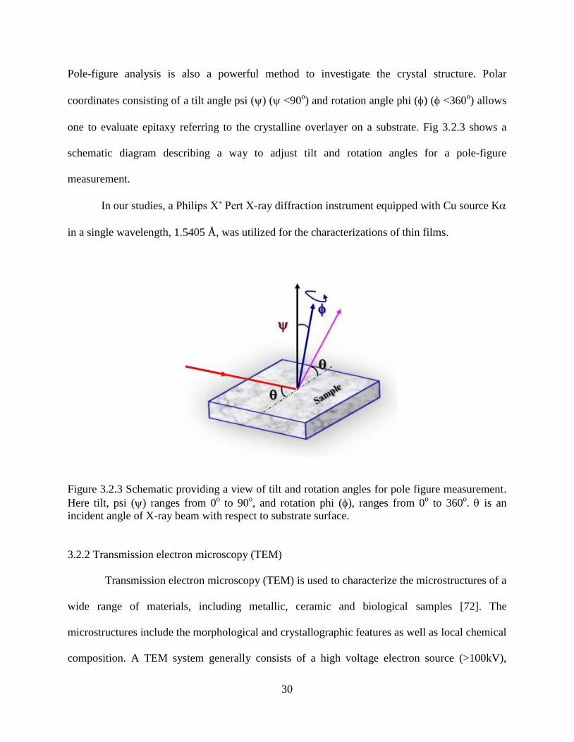
Pole-figure analysis is also a powerful method to investigate the crystal structure. Polar
coordinates consisting of a tilt angle psi () ( <90o) and rotation angle phi () ( <360
o) allows
one to evaluate epitaxy referring to the crystalline overlayer on a substrate. Fig 3.2.3 shows a
schematic diagram describing a way to adjust tilt and rotation angles for a pole-figure
measurement.
In our studies, a Philips X‟ Pert X-ray diffraction instrument equipped with Cu source K
in a single wavelength, 1.5405 Å, was utilized for the characterizations of thin films.
Figure 3.2.3 Schematic providing a view of tilt and rotation angles for pole figure measurement.
Here tilt, psi () ranges from 0o to 90
o, and rotation phi (), ranges from 0
o to 360
o. is an
incident angle of X-ray beam with respect to substrate surface.
3.2.2 Transmission electron microscopy (TEM)
Transmission electron microscopy (TEM) is used to characterize the microstructures of a
wide range of materials, including metallic, ceramic and biological samples [72]. The
microstructures include the morphological and crystallographic features as well as local chemical
composition. A TEM system generally consists of a high voltage electron source (>100kV),

31
electromagnetic focal lenses, a series of lenses to view TEM images, and a columnar ultrahigh
vacuum vessel. The electrons emitted from the source (filament) are accelerated by the high
voltage source and focused through the electromagnetic focal lenses onto a specimen. The
electron beams are scattered by the specimen and then the diffracted beams are brought to focus
by objective lenses on its back focal lens and form a diffraction pattern. Finally, a TEM image or
diffraction pattern can be produced on the fluorescent viewing screen by a series of lenses such
as an objective, intermediate and projection lens.
The TEM imaging and diffraction techniques include TEM bright or dark field, electron
diffraction, high-resolution TEM, and energy-dispersive x-ray spectroscopy (EDS). The bright
field (BF) image is formed by the electrons transmitted through an objective aperture, which is
inserted at the back focal plane of the objective lens. The BF images are used to determine the
size and shape of a specimen. On the other hand, the dark field (DF) image is formed by the
electrons diffracted at the objective aperture. The DF image provides better contrast than BF
image but suffers from low light intensity. Fig. 3.2.4 shows schematics of both BF and DF TEM
imaging modes. The high-resolution (HRTEM) image provides detail information such as a high
magnification image of a specimen down to nanoscale and crystallographic features such as
lattice spacing of the material specimen. The high-energy electrons in TEM cause electron
excitations of the atoms in the specimen. The EDS technique uses the excitation electrons to
provide chemical information of the specimen.
A FEI Tecnai F20-200 keV TEM system was utilized to characterize the microstructures
of MgO nanowries and BaTiO3 or NiFe2O4 coated nanowires in our studies.

32
Figure 3.2.4 Schematic of the TEM image modes. (a) Bright-field image mode (b) Dark-field
image mode. (Adapted from ref. [72]).
3.2.3 Piezoresponse force microscopy (PFM)
PFM is an instrument used to determine local ferroelectric and piezoelectric properties
on the nanoscale [73]. This method images the phase angle from 0o to 180
o as part of
electromechanical response under an externally applied electric field. An AFM tip coated with a
conductive material, e.g., platinum (Pt), scans over a piezoelectric film surface in contact mode
to sense the phase deformation arising from contraction and expansion of the film as a function
of DC bias of the tip. Fig. 3.2.5 is a schematic diagram depicting how the phase deformation is
imaged while the tip is scanned over the surface and senses the degree of displacement. The
sensing signal detected by a photodiode is transmitted to a lock in amplifier to create PFM
images.
Local switching properties are also characterized. For the measurement, a saw tooth-
shaped bias is swept while the tip contacts a local point zone. The phase and amplitude hysteresis

33
loops are obtained owing to local polarization changes corresponding to the sweep voltages.
In this study, MFP-3D (Asylum Research) equipped with conventional atomic force
microscopy (AFM) to acquire surface topography was used to observe ferroelectric polarization
and local switching characteristics of ultrathin films.
Figure 3.2.5 Schematic of typical PFM measurement system. The phase deformation of a sample
is occurred by biased initial tip scans. Then the AFM tip (dashed and solid) indicates the
electromechanical displacement while scanning over the surface and visualizes the phase image
through imaging processes.
3.2.4 Conducting atomic force microscopy (C-AFM)
Conducting AFM (C-AFM) is a technique that provides nanoscale current-voltage (I-V)
characterization of ferroelectric (FE) ultrathin films. During the measurement, a tip serves as a
counter electrode to the bottom metallic electrode so that the basic configuration is tip/FE
barrier/metallic electrode, providing an asymmetric electrode configuration. Fig. 3.2.6 depicts a
schematic of the C-AFM measurement. As seen in the Fig. 3.2.6 a conductive AFM tip scans the
surface of a sample with an applied bias voltage. The tip thereby detects a high or low
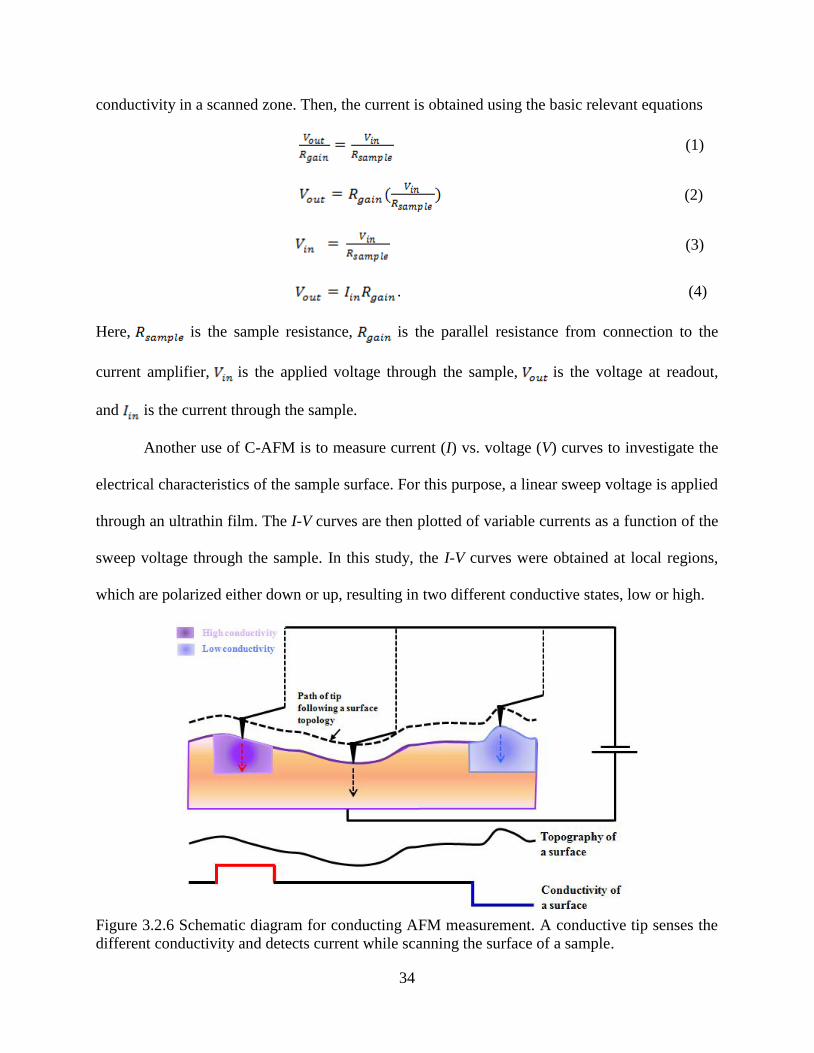
34
conductivity in a scanned zone. Then, the current is obtained using the basic relevant equations
(1)
(2)
(3)
. (4)
Here, is the sample resistance, is the parallel resistance from connection to the
current amplifier, is the applied voltage through the sample, is the voltage at readout,
and is the current through the sample.
Another use of C-AFM is to measure current (I) vs. voltage (V) curves to investigate the
electrical characteristics of the sample surface. For this purpose, a linear sweep voltage is applied
through an ultrathin film. The I-V curves are then plotted of variable currents as a function of the
sweep voltage through the sample. In this study, the I-V curves were obtained at local regions,
which are polarized either down or up, resulting in two different conductive states, low or high.
Figure 3.2.6 Schematic diagram for conducting AFM measurement. A conductive tip senses the
different conductivity and detects current while scanning the surface of a sample.

35
3.2.5 Other characterization methods
Scanning Electron Microscopy (SEM) is a universal technique for studying surface
topology and chemical composition of samples. A SEM system usually consists of an electron
source emitted from a filament, a detector, and a vacuum vessel. The operation is based on
electron interaction with the surface atoms where secondary and back-scattered electrons are
emitted. The detector collects the emitted electrons to visualize images using analysis software.
In this study, a JEOL-7000F FEG-SEM was used for observing the morphology and density of
nanowires.
Reflection High Energy Electron Diffraction (RHEED) is a powerful technique to
investigate the crystal structures of the surface of a sample during film growth. RHEED is
especially used to characterize the diffraction (scatter) pattern on the surface owing to wavelike
properties of electrons as described by quantum physics. The diffraction images help one
determine the crystalline quality of the growing film and growth modes of films, such as layer-
by-layer vs. island mode on a substrate. The RHEED system generally consists of an electron
gun, a detector screen, and an ultra-clean sample. In principle, the electron gun operated in the
range of 10 to 60keV generates electrons, which strike the sample at a low incident angle and the
electrons diffract from the atoms at the surface of the sample. The diffracted electrons create a
diffraction pattern on the detection screen. Fig. 3.2.7 shows the schematic of the RHEED system
A RHEED system equipped with a 30 KeV electron gun (Staib Instruments) was used to perform
the in-situ growth characterization of thin films in our studies.
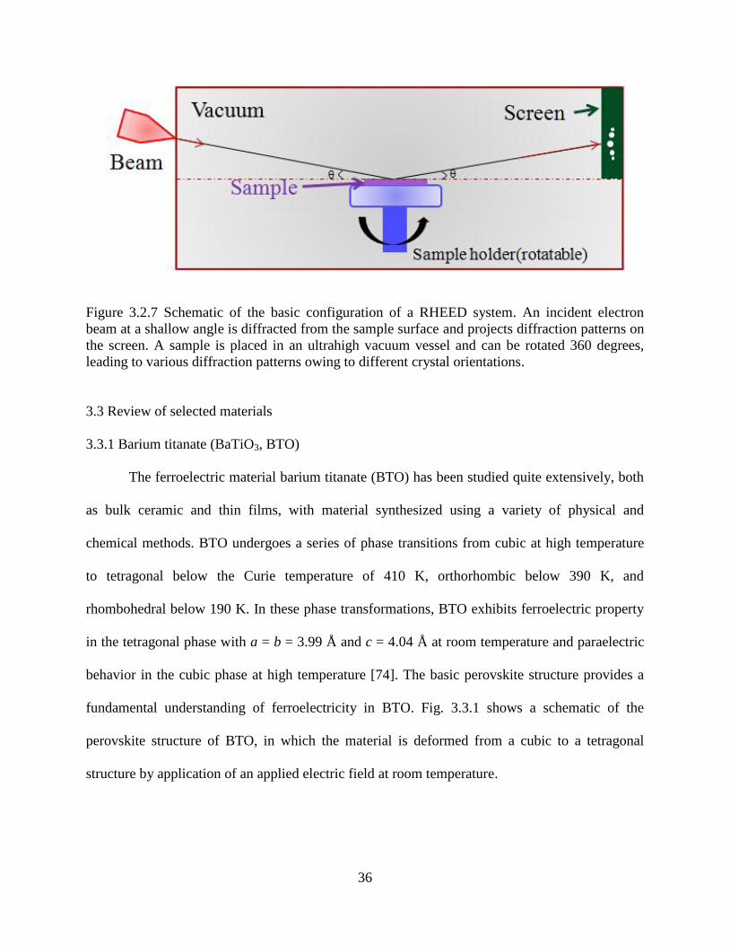
36
Figure 3.2.7 Schematic of the basic configuration of a RHEED system. An incident electron
beam at a shallow angle is diffracted from the sample surface and projects diffraction patterns on
the screen. A sample is placed in an ultrahigh vacuum vessel and can be rotated 360 degrees,
leading to various diffraction patterns owing to different crystal orientations.
3.3 Review of selected materials
3.3.1 Barium titanate (BaTiO3, BTO)
The ferroelectric material barium titanate (BTO) has been studied quite extensively, both
as bulk ceramic and thin films, with material synthesized using a variety of physical and
chemical methods. BTO undergoes a series of phase transitions from cubic at high temperature
to tetragonal below the Curie temperature of 410 K, orthorhombic below 390 K, and
rhombohedral below 190 K. In these phase transformations, BTO exhibits ferroelectric property
in the tetragonal phase with a = b = 3.99 Å and c = 4.04 Å at room temperature and paraelectric
behavior in the cubic phase at high temperature [74]. The basic perovskite structure provides a
fundamental understanding of ferroelectricity in BTO. Fig. 3.3.1 shows a schematic of the
perovskite structure of BTO, in which the material is deformed from a cubic to a tetragonal
structure by application of an applied electric field at room temperature.

37
Figure 3.3.1 Schematic of BaTiO3 (BTO) crystal structure. The BTO material is deformed from
cubic to tetragonal structure by an application of an applied electric field at room temperature.
In the perovskite structure, barium (Ba2+
) ions occupy the unit cell corners and are
surrounded by 12 nearest neighbor oxygen anions (O2-
). The titanium (Ti4+
) metal ion is
positioned at the center of the structure and has six oxygen anions in octahedral coordination as
seen in Fig. 3.3.1(a). When an electric field is applied, the off-center distortion of Ti4+
gives rise
to an electron dipole and phase deformation follows as shown in Fig. 3.3.1(b). Through the
structural transition, BTO exhibits a ferroelectric property with a remnant polarization of value
of 26C/cm2 measured in single crystals.
3.3.2 Nickel ferrite (NiFe2O4, NFO)
Nickel ferrite (NFO) is a well-known insulating and high permeability magnetic material
that is commonly used in transformer cores and microwave applications [75]. The material
possesses a cubic structure (a=8.34 Å) consisting of tetrahedral A sites whose corners are
occupied by oxygen ions and octahedral B sites in which oxygen ions occupy the corners of an
octahedron. Fig. 3.3.2 illustrates the structure in the inverse spinel where divalent ions occupy

38
the B site and trivalent ions are equally split between A and B sites. The net magnetization
(2B/f.u. or 300emu/cm3) in this material is due to the existence of two magnetic sublattices that
results in ferrimagnetic behavior.
Figure 3.3.2 Schematic of inverse spinel NiFe2O4 structure consisting of tetrahedral A sites and
octahedral B sites. The cubic structure is configured by combining these two sites in a FCC
oxygen lattice (Adapted from ref. [37]).

39
3.3.3 Lanthanum strontium manganite (LaSrMnO3, LSMO)
LaSrMnO3 (LSMO) is a half-metallic ferromagnetic material and has a pseudocubic
perovskite structure with lattice parameters a=b=c=3.87 Å. The general formula of the
perovskite is ABO3, where A site is occupied La and Sr ions and B site is occupied by Mn
ions. The magnetic moment of LSMO is approximately 620 emu/cm3
at low temperatures. Its
half-metallic property allows for conduction of spin-polarized electrons. Therefore, LSMO is
widely used a magnetic electrode in combination with an insulating space layer to configure a
TMR system in spintronics [76].

40
CHAPTER 4
MAGNESIUM OXIDE (MgO) and MULTIFERROIC NANOWIRES (NWs)
Reproduced in part with permission from [G. Kim, R. L. Martens, G. B. Thompson, B. C. Kim,
and A. Gupta, J. Appl. Phys., 102 104906 2007]. Copyright [2012] American Physics Society.
4.1 Introduction
We have grown single crystalline MgO nanowires (NWs) both on (001)-orientated
single crystalline MgO and Silicon (Si) substrates. We selected magnesium oxide (MgO)
because of its attractive features for use as the NW template, such as its thermal stability,
chemical inertness, and excellent electrical insulating characteristics.
We employed two methods for nanowire growths: a high-density array and patterned
arrays. The high density array of NWs is produced using a blanket gold thin film as a catalyst.
However, the random placement of the NWs with the high density is a challenge for the
subsequent functionalization and selective placement of the NWs. In contrast, array pattern
formations, such as square cross-section and single dots, offer control over the density of NWs
and have potential for device fabrication. For both the random arrangement and patterned array
methods, a 1 nm thin gold film was electron-beam evaporated onto MgO and Si substrates. For
patterning the gold layer, a positive resist (polymethy methacrylate, PMMA) was spin-coated
onto the substrate surface. The resist-coated layer was patterned in three different square arrays
of dimension 0.25, 1, and 4 µm2 by e-beam lithography. For single dot patterns, a negative e-
beam resist (Fox-12) was spin-coated on a thin gold film deposited on silicon wafer then 10 x 10
arrays were patterned by lithography. Post-patterning, the substrates were ion milled to remove

41
the gold layer except the zone of patterned dot arrays. Final lift-off of the resist on the dots was
accomplished using dilute HF (<1%). Afterwards, single gold dots remained, acting as catalyst
for MgO nanowire growth.
A good correlation was observed between the density, average diameter, and distribution
of the NWs with those of the initial Au catalyst islands formed at the deposition temperature.
Unlike growth with random orientations and sizes on Si, the wires grew vertically on MgO
substrate and exhibited a more uniform size and shape distribution. The latter appear particularly
promising for the selective growth of NWs in pre-patterned regions using electron beam
lithography. As an ultimate objective, the MgO NWs were used as template posts to form core-
shell NWs, BaTiO3 or NiFe2O4 coated nanowires. The successful coated BaTiO3 or NiFe2O4
nanowires propose an appearance of multiferroic nanowire heterostructures.
4.2 Random arrangement of NWs on MgO and Si substrates
4.2.1 Morphologies
The random array of gold nanoparticles generated on the surface of MgO and Si
substrates upon heating, along with the subsequent growth of nanowires (NWs) on these surfaces,
generates two distinct morphologies of NWs, as seen in Fig. 4.2.1. The NWs grow vertically off
from the MgO substrate. In contrast, the NWs on the Si substrate form a „basket-weave‟ like
morphology, being intertwined and at various non-vertical growth directions. The inset images of
Fig. 4.2.1 show the morphology and density of gold nanoparticles, which are formed from the
ultrathin gold film and act as the catalyst for the vapor-liquid-solid (VLS) growth mechanism of
the MgO NWs. These particles form a discontinuous array of semicircular-shaped nanometer-
sized particles because of overall reduction of the surface tension at this high temperature. The
average length of the MgO nanowire grown on MgO substrate is ~1 m for a deposition period

42
of 60 minutes. On the other hand, the wires grown for the same time period on Si substrate are
significantly longer. The overall reaction leading to the formation of the MgO nanowires from
the precursor can be represented by the chemical reaction
2Mg3N2(g) → 6Mg(g) + 2N2(g) + 3O2 (g, added) + Ar (g, added) → 6MgO(s) + 2N2(g) + Ar(g).
The small added concentration of oxygen with the argon carrier gas is likely adsorbed on
the surface of the gold catalyst and reacts with the magnesium vapor to form the initial nuclei
that results in the growth of MgO NWs. For Si NWs, Kodambaka et al. [77] have reported that
the ambient oxygen concentration reduces the gold diffusion along the sidewalls during growth
process enabling the NW to grow longer and have an untapered geometry. On the other hand,
Kazuki et al. [78], based on their MgO NW growth experiments using PLD, have suggested that
the total ambient pressure (either argon or oxygen) and not the actual oxygen content which gets
incorporated into the MgO wires is critical for enhancing the NW growth. Nonetheless, they
observed that the oxygen concentration is critical for the degree of crystallinity of the MgO wires.
The Au nanoparticle usually „rides‟ atop the growing structure and its size remains essentially
unchanged during the entire process of the wire growth, as has been previously observed in other
VLS grown structures [79]. However, under non-optimal growth conditions, the gold catalyst
can diffuse away during growth and the wire‟s height can be shunted [80]. The SEM images of
Fig. 4.2.1 show gold particles at the tip of the longer wires indicating limited gold catalyst
diffusion away from the tip of the wire under our operating conditions. TEM images and
diffraction patterns, shown in Fig. 4.2.2, indicate that the NWs have a rectangular cross-section
with <001> growth direction. This growth direction is to be expected based upon the
homoepitaxy between the MgO NW and the MgO (001) substrate at these processing
temperatures.

43
Figure 4.2.1 SEM images showing the growth of vertically aligned MgO nanowires on a (001)-
oriented MgO substrate. The inset shows an image of the gold particles formed by heating the
gold film on the MgO substrate to the growth temperature and then cooled down without actual
growth of the nanowires. (b) SEM image showing MgO nanowires grown on a (001)-oriented Si
substrate for a total deposition period of 60 minutes. The wires grow in random directions
exhibiting a basket-weave-like morphology. The inset shows the gold particles formed by
heating the gold film on the Si substrate to the growth temperature and then cooled down without
actual growth of the nanowires. The marker for both inset images is 100 nm. (Reproduced with
permission from ref. [81])
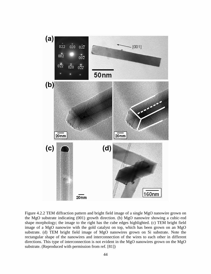
44
Figure 4.2.2 TEM diffraction pattern and bright field image of a single MgO nanowire grown on
the MgO substrate indicating (001) growth direction. (b) MgO nanowire showing a cubic-rod
shape morphology; the image to the right has the cube edges highlighted. (c) TEM bright field
image of a MgO nanowire with the gold catalyst on top, which has been grown on an MgO
substrate. (d) TEM bright field image of MgO nanowires grown on Si substrate. Note the
rectangular shape of the nanowires and interconnection of the wires to each other in different
directions. This type of interconnection is not evident in the MgO nanowires grown on the MgO
substrate. (Reproduced with permission from ref. [81])

45
Unlike the MgO substrate, the nanowires are not epitaxially anchored onto the (001) Si substrate.
Moreover, a pristine Si surface is not presented during the growth since the partial pressure of
oxygen, particularly at these processing temperatures, will enhance the natural oxidation of the
Si surface. As the MgO wires nucleate and grow in length, the lowest surface energy facets will
dominate and preferentially grow in which every direction they are formed. All the NWs that we
have imaged, grown to different heights and on different substrates, exhibit the square rod shape.
In general, the {001} facets in rock-salt-crystals, such as MgO, have the lowest surface energy
[82], allowing the wires to maintain the cubic shape facets perpendicular to the axial growth
direction of the wires on MgO substrate. In contrast, since the nucleation of nanowires is not
fixed to any particular direction from the Si substrate, as Colli et al. [83] have reported for ZnO
nanowires on Si, they grow outwardly in multiple directions and develop the basket-weave
morphology.
4.2.2 Histograms of MgO NWs and gold nanoparticles
The cube-length of the rectangular nanowires, termed “diameter,” has been measured
from the TEM images. A comparison of the wire diameters in Fig. 4.2.3 shows that the average
diameter is 19 ± 5 nm and 29 ± 13 nm for the MgO and Si substrates, respectively. Additionally,
the Si substrate shows a greater wire-to-wire diameter variability.
A histogram comparing the initial gold particle sizes between the two substrates is
graphed in Fig. 4.2.4. The average gold particle diameters were found to be 23 ± 7 nm and 51 ±
11 nm and for the MgO and Si substrates, respectively. Similar to the wire variability, the Si
substrate gold particles show a wider size distribution. This is likely due to differences in the
surface tension between liquid Au-Si and liquid Au-MgO interface. Metal films grown on oxide
surfaces are known to significantly „ball up‟ because of the high surface tension [84].

46
Figure 4.2.3 Histograms comparing the diameter of MgO nanowire grown on (a) MgO (001),
and (b) Si (001) substrates. (Reproduced with permission from ref. [81])

47
By providing thermal energy, as in our growth process, the metal surface mobility is
enhanced resulting in both the driving force and mobility to produce small metal particles on the
oxide surface that have little variability in the contact angle. The larger average size and larger
range of sizes of the gold catalysis particles invariably contribute to the variability in the wire
diameters. Additionally, the random basket-weave morphology of the nanowires on Si substrate
will hinder uniform growth because of the tortuous diffusion path for transporting the precursors
to the growing wires. Collectively, this will contribute to different growth rates for each wire
depending upon its location. In contrast, the nearly uniform gold catalyst particle sizes and
vertical growth direction of the wires from the MgO substrate provide for more consistent
growth conditions and reduced variability in the final wire size. Additionally, for MgO substrate
wires, there is no appreciable diameter variation along the ~ 1µm axial length of the wires. Based
on the random array results, we have ruled out Si as an adequate substrate for selectively
patterning well-ordered nanowire arrays. The selective patterning has thus only been performed
on the MgO (100) substrates.
4.3 Systematic pattern array of MgO NWs on MgO substrate
4.3.1 Square cross-section pattern
A series of gold catalysis regions have been selectively patterned into different regions
of 0.25, 1, and 4 µm2. The SEM images, shown in Fig. 4.3.1 (a), (b) and (c), depict different
number of freestanding MgO nanowires grown in the various gold pattern regions, respectively.
The regions over which the wires grow are approximately 50% larger than the initially patterned
square areas. At 925oC, the liquid-like gold layer has enhanced mobility and is likely to spread
out and extend beyond the patterned areas. The density of nanowires at each patterned area is
typically in the range of 200 - 250 per m2.

48
Figure 4.2.4 Histograms comparing the size of gold nanoparticles formed using a 1 nm thick
gold film on (a) MgO (001) and (b) Si (001) substrates. (Reproduced with permission from ref.
[81])

49
A histogram comparing the gold nanoparticles sizes formed at the reaction temperature in
patterned regions of 1 m2 is shown in Fig. 4.3.2 (measured at room temperature).
The properties of patterned nanowires are summarized in Table 4.3.1. For each patterned
region, the wires exhibit fairly good uniformity in both size and quantity. Additionally, changing
the size of the pattern area does not appear to dramatically alter the wires sizes or packing
density between the different regions studied. The abilities to selectively pattern wires into
specific locations and control the shape, size and density provide the capability to functionalize
and manipulate these structures for the fabrication of nanoscale devices.
4.3.2 Single dot pattern
Single free-standing MgO NWs were grown in 10 x 10 dot arrays. In order to carry out
this synthesis, e-beam lithography was used to prepare a pre-patterned dot array as seen in SEM
image of Fig. 4.3.3(a). Here, each dot size is approximately 200 nm in diameter. Single MgO
NWs were grown on the gold dot arrays as seen in Fig. 4.3.3(b). The height of NWs is
approximately 5-10 m and the distance between wires is 1 m. Since the dot size diameter is
bigger than the radius of NWs, two or three NWs were grown within the same gold dot zone in
some case. However, our work clearly demonstrates that single vertically arrayed MgO NW can
in principle be synthesized at specifically selective points or regions. Thus, this technique
appears suitable for well-controlled growth of NWs both in terms of their position and density.
This is important to avoid shadowing effect during film deposition on the NWs and provide
excellent uniformity and control of a sheath thickness.

50
Figure 4.3.1 SEM images showing different patterned regions of the MgO nanowires. The bright spot on the top of each nanowire is
the gold catalyst particle. [(a) and (d)] 0.25m2, [(b) and (e)] 1m
2, and [(c) and (f)] 4m
2. A blanket gold film of 1 nm thickness is
deposited and patterned using e-beam lithography for the selective growth of the nanowires. (Reproduced with permission from ref.
[81])

51
Figure 4.3.2 Histogram of the size distribution of gold nanoparticles formed within the 1m2
patterned regions on an MgO (001) substrate. The average nanoparticle size is 20 nm.
(Reproduced with permission from ref. [81])
TABLE 4.3.1 Tabulation of the absolute number and density of the grown nanowires at different
patterned area, along with the number of gold catalyst particles formed at the growth temperature.
(Reproduced with permission from ref. [81])
Measurement Square area (m2) 0.55 1.5 6.4
Number of nanowires 124 297 1092
Density of nanowires (m-2
) 225 198 170
Size of gold nanoparticles (nm) 194.9 20.47.2 18.44.2

52
Figure 4.3.3 SEM images of a single MgO NW (a) Gold dot pattern in 10 x10 arrays. The
diameter of dots is approximately 200 nm. (b) Single MgO NW grown within each dot array.
The height is around 5-10m.

53
4.4 Multiferroic nanowires
Bilayer BaTiO3 (BTO) and NiFe2O4 (NFO) films deposited on the MgO nanowires can
be used as a multiferroic composite with significantly reduced clamping effect as compared to
2D structures. Fig. 4.4.1 illustrates the fundamental concept to form the multiferroic NW
composite. Vertical free-standing MgO NWs are initially synthesized as shown schematically in
Fig. 4.4.1(a). The pulsed laser deposition (PLD) technique deposits binary thin coatings on to the
MgO NWs as shown in Fig. 4.4.1 (b)-(c), where a ferroelectric sheath layer is deposited on the
initial ferrite layer. Fig. 4.4.1 (d) shows a cross section of the multiferroic NW. In order to
synthesize the coaxially coated multiferroic nanostructures, we have used isolated MgO NWs
grown on MgO substrate as templates because of the high thermal stability, lattice match,
chemical compatibility, and vertical growth.
Prior to fabricating coaxially-coated NWs, thin BTO or NFO films were deposited as
two-dimensional (2-D) structures via PLD. We selected these two materials because of their
excellent lattice match with MgO, as shown in table 4. 4.1. The grown films were characterized
using Philips XPer XRD to determine their crystallinity and RHEED for in situ monitoring the
film growth mode in a real time. The results are promising for the successful film growth on the
template MgO NWs to form multiferroic nanowires.
TABLE 4.4.1 Lattice parameter (a) and lattice mismatches (%) for each material.
Lattice parameter (Å) Lattice mismatch a/a (%)
MgO NiFe2O4 BaTiO3 NiFe2O4 BaTiO3
4.2 8.34 3.99
-0.7 -5
a/a =(afilm-asub)/asub [asub is bulk lattice parameter, - tensile strain]
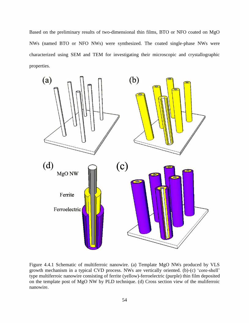
54
Based on the preliminary results of two-dimensional thin films, BTO or NFO coated on MgO
NWs (named BTO or NFO NWs) were synthesized. The coated single-phase NWs were
characterized using SEM and TEM for investigating their microscopic and crystallographic
properties.
Figure 4.4.1 Schematic of multiferroic nanowire. (a) Template MgO NWs produced by VLS
growth mechanism in a typical CVD process. NWs are vertically oriented. (b)-(c) „core-shell‟
type multiferroic nanowire consisting of ferrite (yellow)-ferroelectric (purple) thin film deposited
on the template post of MgO NW by PLD technique. (d) Cross section view of the muliferroic
nanowire.

55
4.4.1 Thin BaTiO3 and NiFe2O4 films
X-ray diffraction (XRD) measurements, including -2 scans, rocking curve, and pole-
figure, were carried out to characterize crystallinity of the 2-D thin films. Fig. 4.4.2(a) shows
XRD -2 scans of single-phase NFO and BTO film grown on MgO substrate. The peak position
for the BTO film is very close to that for bulk BTO, with a slight shift to the left of the bulk
value (somewhat larger out-of-plane lattice parameter). Thus, the BTO film is essentially
relaxed. In contrast, the peak position of NFO film shows a significant shift to the right of the
bulk value (smaller out-of-plane lattice parameter), indicating an in-plane tensile strain. Rocking
curves in Fig. 4.4.2(b) show narrow curves for both BTO and NFO film, indicating excellent
crystallinity. The full-width-half-maximum (FWHMs) values are 0.03o and 0.038
o, respectively.
Fig. 4.4.2 -2 X-ray diffraction spectra for a single-phase NFO and BTO film on MgO substrate.
Peaks are close to the angular positions of the (004) and the (002) reflection of NFO and BTO.
(b)-(c) Rocking curves for NFO and BTO films. The vertical solid lines indicate the bulk NFO
and BTO 2 peak positions. Here, makers, *, , and , indicate MgO bulk peak, NFO and BTO
film peaks.

56
Figure 4.4.3 Phi scans of (311) reflection of bilayers of NFO and BTO films on MgO. Four
symmetric peaks spaced 90 degrees apart are observed.
X-ray Phi scans () were carried out on the off-axis (001) and (311) plane of the films.
Fig. 4.3.3(a) and (b) show the peaks with four-fold symmetry of both the films grown on MgO.
The peaks show the same azimuthal angle, being 90 degrees apart, indicating cube-on-cube
growth.
RHEED was used to in-situ monitor the crystallinity and initial growth mode of films in
real time during PLD deposition. Fig. 4.3.4(a) shows well-defined lattice rods of MgO substrate
prior to deposition, displaying a perfect single crystal structure. Fig. 4.3.4(b) and (c) show
RHEED patterns of BTO and NFO film grown on MgO substrate. Remarkably streaky RHEED
patterns are observed, revealing excellent single crystal structure of both films.

57
Figure 4.4.4 RHEED patterns along [100] for epitaxial growth of BTO and NFO thin films on
(100)-oriented MgO substrate. (a) RHEED image of MgO substrate prior to deposition. (b)-(c)
RHEED image of BTO and NFO films.

58
4.4.2 Single phase BaTiO3 or NiFe2O4 coated NWs
Ferroelectric or ferromagnetic coated BTO and NFO NWs were characterized using
SEM and TEM. The SEM images of template MgO, BTO and NFO NWs are shown in Fig.
4.4.5. The MgO NWs with gold balls on top of the NWs are clearly observed, as seen in Fig.
4.4.5(a) where the NWs are free standing and well separated. In addition, SEM images of coated
BTO and NFO NWs are shown in Fig. 4.4.5 (b)-(c). The images clearly show thicker BTO or
NFO-coated NWs than the initial MgO NWs and bright contrast because of electron charging
effect from the coated NWs, which are insulators.
For investigating the morphologic properties of BTO-coated NWs, TEM
characterization was performed. Fig. 4.4.6(a) shows the bright field TEM image of a single BTO
NW that is 10 m in length and 150 nm in diameter. The insert image shows the diffraction
pattern of the BTO, indicating a well ordered crystalline structure. The geometry of BTO-coated
NW is cubic rod-shaped as shown in Fig. 4.3.6(b). The shape is expected based on the epitaxy
relationship with the initial MgO nanowire. The shape also reveals that conformal coating by
PLD occurs on the template MgO nanowire. High resolution TEM (HRTEM) images in Fig.
4.4.6(c) shows a highly ordered heterostructure, with <001> growth direction and good
crystallization with lattice spacings of 3.98 Å and 4.2 Å. These spacings correspond to the
distance between the (001) planes of BTO and the MgO NW, respectively. This provides further
evidence of the heteroepitaxial growth of BTO on the template MgO NWs. The drawn white
lines clearly demarcate the boundary between MgO and BTO. Excellent lattice stacking and no
defects are observed at the interface of BTO and MgO. Energy dispersive x-ray spectroscopy
(EDS) analysis clearly shows Ba, Ti, Mg, and O, as shown in Fig. 4.4.6(d), confirming
successful growth of coated BTO-NWs.

59
Figure 4.4.5 SEM images of nanowires. (a) Template MgO NWs. Gold balls lifted up and
positioned on top of MgO NWs during a growth. (b) Single-phase BTO NWs. (c) Single-phase
NFO NWs.
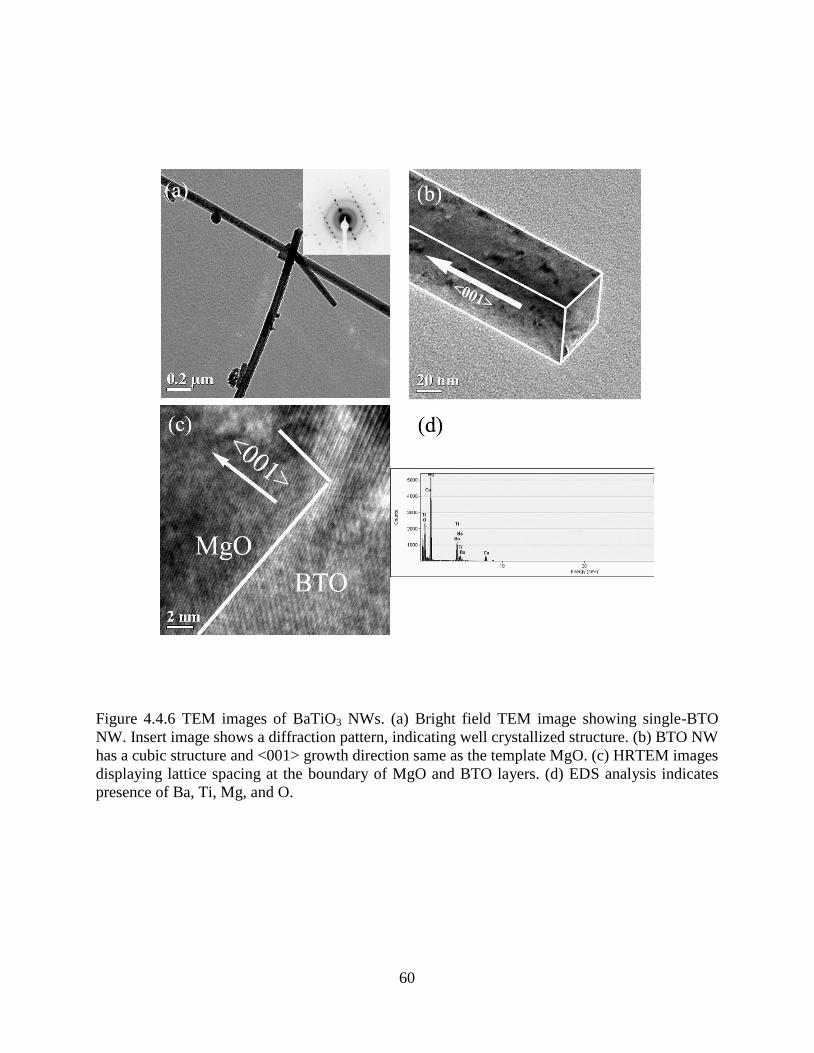
60
Figure 4.4.6 TEM images of BaTiO3 NWs. (a) Bright field TEM image showing single-BTO
NW. Insert image shows a diffraction pattern, indicating well crystallized structure. (b) BTO NW
has a cubic structure and <001> growth direction same as the template MgO. (c) HRTEM images
displaying lattice spacing at the boundary of MgO and BTO layers. (d) EDS analysis indicates
presence of Ba, Ti, Mg, and O.

61
TEM characterization was also performed on the NFO-coated NWs. Fig. 4.4.7(a) shows a
bright field image of NFO-coated NWs. The insert image shows the diffraction pattern of the
NW, revealing a well-ordered and crystalline structure. The NFO-coated NWs have cubic rod
shape morphology as shown in Fig. 4.4.7(b), which is similar to the BTO-coated NWs. A high-
resolution TEM (HRTEM) image in Fig. 4.4.7(c) shows an ordered heterostructure of NFO NW,
indicating good crystallinity with lattice spacing of about 4.2 Å. The boundary of NFO and MgO
is not very clear because of the similar lattice parameters. The growth direction of NFO-coated
NW is [001], the same as the direction of template MgO NWs, revealing heteroepitaxial growth
of NFO. Energy dispersive x-ray spectroscopy (EDS) analysis clearly shows Ni, presence of Ni,
Fe, Mg, and O, shown in Fig. 4.4.6(d), confirming the successfully coating of NFO on the MgO
template NWs. The successful growth of single-phase BTO and NFO coating on MgO NWs
shows promise for synthesizing binary NFO/BTO multiferroic heterostructures using PLD.

62
Fig. 4.4.7 TEM images of NiFe2O4 NWs. (a) Bright field TEM image showing single-NFO NW.
Insert image shows a diffraction pattern, indicating well crystallized structure. (b) NFO NW has
a cubic structure and <001> growth direction, same as the template MgO. (c) HRTEM image
displaying lattice spacing of MgO and NFO layers. The lattice spacings cannot be resolved
because MgO and NFO are isostructural with very similar lattice parameters. (d) EDS analysis
indicates presence of Ni, Fe, Mg, and O.

63
4.5 Summary
MgO NWs have been successfully synthesized using the VLS method. Depending on the
substrate and placement of the Au catalyst, the nanowires can have uniform diameter and display
position-controlled growth. The size variability of the NWs can be directly correlated with the
variability in the size of the gold catalyst particles and the extent of uniformity in the growth
morphology. The MgO NWs grow homoepitaxially normal to the MgO substrate, whereas the
wires grown on the Si substrate exhibit a variety of different growth directions even though they
are all single crystalline. On both MgO and Si, the nanowires exhibit a <001> growth direction,
as determined using TEM. Using e-beam lithography, selective synthesis of MgO NWs in square
cross-sections has been achieved with control on both the size and density of the wires. Upon
annealing the patterned gold film to the growth temperature of the wires, the patterned regions
expand beyond the original dimensions but reasonably maintain the original shape. In addition,
vertically free standing single MgO NW arrays were successfully grown. The patterning and
growth of MgO NWs with control on their placement is attractive for their use as template posts
for functionalization and for device fabrication and integration. Single-phase BTO and NFO-
coated NWs were fabricated by coating the template MgO NWs. The successful growth promises
the binary-coated NW formation, which is going to be a prototypical structure of multiferroic
nanowire. Detailed process set up and understanding of the multiferroic NWs remain a future
research task.

64
CHAPTER 5
NANOSCALE ELECTRORESISTANCE PROPERTIES OF ALL-OXIDE MAGNETO-
ELECTRIC TUNNEL JUNCTION WITH ULTRA-THIN BARIUM TITANATE BARRIER
Reproduced in part with permission from [Applied Physics Letters], submitted for publication.
Unpublished work copyright [2012] American Physics Society.
5.1 Introduction
Magnetoelectric and Multiferroic Tunnel Junctions (METJs and MFTJs) are an emerging
paradigm for device applications [85]. They provide the basis for a new class of solid-state
memory devices, which are non-volatile and both electrically and magnetically tunable, and
sometimes referred to as magnetoelectric random access memory (MERAM) devices.
Fundamentally, METJs combine both tunnel electroresistance (TER) and tunnel
magnetoresistance (TMR) effects [13, 15]. While room-temperature TMR effect has been known
for almost 20 years, TER effect has only been recently reported, thanks largely to advances in
oxide thin-film growth. A giant TER effect was demonstrated on highly strained BaTiO3 (BTO)
barrier layers deposited on thin ferromagnetic La0.67Sr0.33MnO3 (LSMO) or SrRuO3 (SRO)
electrode layers [86, 87]. A tunnel effect by current (I)-voltage (V) measurements were equally
presented to exhibit a resistance switching by the polarization directions. Similar results were
also reported for BiFeO3 (BFO) and PbTiO3 (PTO) [19, 88]. All these experiments verify the
earlier theoretical prediction of the TER effect [18, 32, 89]. More recently, proof-of-concept
METJ devices have been successfully demonstrated at low temperatures [ref. 86]. These findings

65
have resolved, or at least alleviated, some of the longstanding concerns about the applicability of
ferroelectric materials in devices requiring ultra-thin layers.
To integrate the METJ, such heterostructures consist of an ultrathin ferroelectric or
multiferroic material as the active tunneling barrier sandwiched between ferromagnetic
electrodes. Here, an ultrathin ferroelectric film of a few unit cell thicknesses is required for the
active tunneling barrier; otherwise there is no tunnel current across the barrier because of the
scattering effect of carries. The challenge is to fabricate ultrathin films that retain the robust
ferroelectric properties because of the critical thickness limitation, losing the ferroelectric
property due to the depolarization by a reverse behavior below the critical thickness [33].
In this study, we investigated the thin-film heterostructure prototype consisting of
ultrathin ferroelectric BaTiO3 (BTO) and ferromagnetic La0.67Sr0.33MnO3 (LSMO). We have
quantified nanoscale ferroelectric and transport properties of this METJ prototype by using
scanning probe microscopy techniques. Through local I-V measurements we demonstrate robust
TER effect in ultra-thin BTO tunnel barriers of only 1.2 nm thickness, which is thinner than the
calculated critical BTO film thickness (2.4 nm) [90]. Combined with earlier experimental reports
[87, 91], we show that METJs have the ability to scale down (i.e., retain their functionality) to a
level that current spintronics devices can offer.
The La0.67Sr0.33MnO3/BaTiO3 (LSMO/BTO) heterostructures were deposited on (001)-
oriented SrTiO3 (STO) substrates using the pulsed laser deposition (PLD) technique (Lambda
Physik KrF excimer laser, =248 nm). LSMO thin films of 30 nm thickness were grown with
200 mTorr background oxygen pressure and laser fluence of 1.5 J/cm2 and 2 Hz repetition rate.
Then an ultrathin BTO films were deposited at an oxygen pressure of 10 mTorr at 5 Hz on the
LSMO serving as a bottom electrode. The thicknesses of the BTO films as a tunnel barrier layer

66
range from 1 nm to 2 nm. Both LSMO and BTO films were deposited at an identical substrate
temperature of 700oC. Film thickness for all layers was calibrated using an x-ray reflectivity
technique.
Measurements were performed using the MFP-3D (Asylum Research) scanning probe
microscope (SPM). We used conductive platinum-coated silicon (DPER-18), platinum (Pt)-
silicide (Si) (PtSi) and diamond-coated tips (CDT) for the conducting atomic force microscopy
(C-AFM) measurements. The tips vary in terms of their resistivity, contact area characteristics
and degree of degradation with usage. Table 5.1.1 summarizes the properties of the tips.
Table 5.1.1 Comparison of properties of three different conductive tips.
Contact
Area (nm2)
Tip Material Wear-out
Condition
Frequency
(kHz)
Force constant
(N/m) Vender
DPER
18 ~10
2
Platinum
coated High 75 3.5 Mikromash
PtSi ~103
Platinum and
Silicide Middle 330 42 Nanoworld
CDT ~104
Highly doped
Diamond Low 400 80 Nanoworld
The SPM was used primarily in the piezoresponse force microscopy (PFM) and
conducting AFM (C-AFM) mode. PFM allows us to investigate and control the local ferro- and
piezo-electric properties, while the C-AFM was utilized to observe the dependence of the
tunneling properties of the barrier on the polarization state as a function of applied bias. To
perform the writing operation of different polarization states, the BTO film was poled by
applying either a negative or positive tip bias. Reading of the polarization states was achieved by

67
a conventional PFM imaging method. In addition, local ferroelectric switching properties were
characterized by a switching spectroscopy method in which a saw tooth-shaped bias voltage was
swept with the tip in a contact mode, while measuring the piezoelectric phase and amplitude.
In order to investigate the local current (I) vs. voltage (V) characteristics, a linear sweep
voltage was applied and then I-V curves were obtained by measuring the current as a function of
sweep voltage for different ferroelectric polarization states.
5.2 Experimental results and discussion
5.2. Piezoelectric properties of the ultrathin BaTiO3 films
AFM micrographs of 2 nm BTO films grown on 30 nm LSMO bottom electrode show an
atomically-flat surface with root-mean-square (rms) roughness of 0.2 nm as seen in Fig. 5.2.1.
The films are essentially free of nanodroplets that are typically associated with the PLD process.
Robust ferro- and piezo-electric properties of the BTO films are observed on patterned
polarized regions, as seen in Fig. 5.2.2 (a), (b). The University of Alabama logo has been used to
generate the pattern. The pattern was processed by applying a positive or negative bias voltage to
generate different polarization states in a white and black zone as seen in Fig. 5.2.2(a). The bias
voltage is applied through a conductive tip with the LSMO film serving as the ground electrode.
The characteristic piezoelectric response of the film was clearly demonstrated as different color
contrasts for the two polarization states, illustrating a clear elephant image as shown in Fig.
5.2.2(b). The dark brown color corresponds to the regions poled by negative bias voltage, while
the light brown region reflects the positively poled areas.
Nanoscale ferroelectric properties of the 2 nm BTO film have been quantified using a
switching spectroscopy PFM method, [92] as seen in Fig. 5.2.3. We placed a conductive tip on a

68
single point region and swept the bias voltage over a range larger than the coercive field to
obtain fully saturated polarization switching loops. The polarization reflected ferroelectric
hysteretic behavior is clearly observed in Fig. 5.2.3(a) along with a butterfly-shaped loop for the
phase in Fig. 5.2.3(b). Both hysteresis loops show similar result of hysteresis loops as measured
for a 4.8 nm BTO film [87]. However, a complete 180 degree phase reversal is not observed.
This is likely due to depolarization behavior, which has previously also been observed for
ultrathin films that are close to the critical thickness for ferroelectricity [33]. The depolarization
is caused by displacement of Ti4+
closer to the symmetric central position in the perovskite
structure with reduced polarization.
Figure 5.2.1 AFM surface topology image of BTO film of thickness 2 nm. RMS roughness of the
film is 0.2 nm.

69
Figure 5.2.2 Schematic for generating polarization pattern (a) and a polarized image showing UA
logo with an elephant (b). Black color zone is written using a tip voltage, Vtip = - 3V and white
color is zone is written using a tip voltage, Vtip = + 3V.

70
Figure 5.2.3 Hysteresis loop corresponding to polarization switching of BTO film. (a) Phase map
in degree and (b) amplitude map exhibiting a butterfly loop.
To systematically control the UP-DOWN polarization states (UP implying polarization
vector pointing towards the tip), a 2 µm x 2 µm square area is first poled in the downward
direction using a negative tip bias of -3 V (Fig. 5.2.4(a-1)) and then a 0.7 µm x 0.7 µm square
region in the center is reverse-poled by a positive tip bias of +3 V (Fig. 5.2.4(a-2)). The dark and
light PFM contrast of a larger 3 µm x 3 µm square area (Fig. 5.2.4(b)) shows clearly the different
polarization states in the two regions. We further successfully have rewritten a rectangular area
in the top region of the polarized pattern by applying a positive bias voltage after the initial
patterning process (Fig. 5.2.4(a-3)). The re-read PFM image is seen in Fig. 5.2.4(c). We also
confirmed that Fig. 5.2.4 (c) image is retained for at least three days. These results indicate that
ultrathin 2 nm BTO films exhibit robust and reproducible piezoelectric/ferroelectric properties.
Qualitatively similar results have been obtained with a 1.2 nm (3 unit cells) thick BTO film on
LSMO, although the PFM contrast is not as sharp as that for the 2 nm film.

71
Figure 5.2.4 Schematic illustration for creating different polarization state regions. (a-1) 2m ×
2m square zone poled by a negative voltage. (a-2) 1 m × 1m center region poled by a
positive voltage. (a-3) is re-poled area by a positive voltage after 6 hours. (b) PFM image after
initial polarization resulting from steps (a-1) and (a-2). (c) Re-read PFM image after step (a-3).
5.2.2 Conductive properties of the ultrathin BaTiO3 films
Local tunneling properties of ultrathin BTO film have been investigated by measuring the
current-voltage (I-V) characteristics using C-AFM technique. Measurements shown here are
performed on ferroelectric BTO thin films of thickness 1.2 nm. We primarily used commercial
conductive diamond coated tips for the C-AFM measurements as they have a large tip area,
which gives better contact, while the hardness of diamond provides low degree of tip wear
during scans. Firstly, we acquired current-maps where the tunnel current is measured during
typical raster-scans while maintaining the tip at 1 Volt (Fig. 5.2.5).
Prior to performing these measurements, an UP (DOWN) polarization state is generated
by applying a high positive (negative) voltage through the sample with the tip acting as a virtual
ground (Fig. 5.2.5 (a), (c)). In Fig. 5.2.5 (b) and (d), we show a typical current-map of a 0.5 µm x
0.5 µm area of the BTO/LSMO heterostructure with upward and downward polarization
orientations, respectively. The bright gray (green) color indicates a relatively high (low) tunnel
current in the case of polarization pointing upward (downward). This is the TER effect,

72
described as the change in the resistance of the thin BTO/LSMO heterostructure arises from the
switching of the polarization orientation [18]. Even though there are some local variations in the
tunnel current, our data clearly shows that the TER effect is robust over large areas of the
BTO/LSMO heterostructure.
To further quantify the TER effect, local current (I) - voltage (V) measurements have
been carried out by locally applying a sweep voltage ranging between + 0.5 V to - 0.5 V after
creating one of the two polarization states in the sample. As Fig. 5.2.6 clearly indicates,
significantly higher current (lower DC resistance) is observed for the UP state as compared to the
DOWN state for all bias voltages. We refer to the high current (low resistance) state as the ON
state and the low current (high resistance) state as the OFF state. This data, again, confirms the
TER effect is robust down to a barrier thickness typically found in commercial hard-drive read-
heads with MgO tunnel barrier. Calculation of the resistance ratio between two polarization
states reveals a value of up to 60 at low bias (inset of Fig. 5.2.6), which is comparable to the
reported values in ref. [86].

73
Figure 5.2.5 Schematic of configurations for polarization orientation. (a) Polarization pointing
upward by application of a positive sample bias. (b) Current map while scanning the region. (c)
Polarization pointing downward by application of a negative sample bias. (d) Current map while
scanning the same region. For the measurements the tip is grounded and the current is measured
using an amplifier.

74
Figure 5.2.6 I-V curves measured with different polarization states, upward or downward,
corresponding to switch ON or OFF state. The black lines represent I-V curves fits using the
Brinkman model. Insert shows the TER and ON/OFF ratio

75
Detailed characterization of the TER effect has also been performed with two other
commercial tips. Both PtSi and DPER-18 tips exhibit lower tunnel current as seen in Fig. 2.5.7
(a) and (c), primarily because of the small contact area (~102 nm
2). The corresponding resistance
ratios between the two polarization states as seen in Fig. 5.2.7 (b) and (d) are also substantially
smaller as compared to the conducting diamond tip, with values between 10-30 being observed
at low bias voltages. We must mention that tip degradation is especially severe during local I-V
characterization, particularly for the PtSi and DPER-18 tips, and only the few first passes with a
brand new tip yield any measurable current. The characterizations shown here are, therefore,
confirmed through measurements with numerous tips.
The experimentally obtained I-V curves have been fitted with the Brinkman model
assuming a trapezoidal potential barrier to obtain information about the average barrier height
[93]. The black solid line in Fig. 5.2.6 shows the simulated I-V curve. As clear, the experimental
points (solid red and blue dots) are well-matched with the theoretical fit (black solid lines).
According to the Brinkman model, the conductance is expressed by the polynomial
(1)
where A, B, and C can be evaluated by fitting the experimental I-V curves. Based on the values
of the constants A, B, and C, one can calculate the barrier height () in eV, barrier asymmetry
() in eV, and barrier thickness (d) in Å
(2)
(3)

76
Figure 5.2.7 I-V curves and TER values measured by DPER 18 (a)-(b), and PtSi (c)-(d)
commercial tips at different polarization states, upward or downward, corresponding to switch
ON or OFF state.

77
(4)
. (5)
Using eq. (2-5) for the different polarization states, ON and OFF, we calculated film thickness,
barrier height, and barrier asymmetry due to three commercial tips. Table 5.2.1 summarizes the
results. The fitted film thickness is between 3-4 nm, which is higher than the experimental film
thickness of 1.2 nm. We believe that the discrepancy is due to the simplicity of the theoretical
model, which does not consider experimentally involved conditions such as interaction of the
tips with the sample, BTO film surface morphology and roughness, and other tip-induced effects
during the measurement.
The barrier heights determined using the different tips when fitted with the Brinkman
model are compared as shown in Fig. 2.5.8. The CDT and DPER-18 tips provide lower barrier
height values for the ON state as compared to the OFF state. The average barrier height values
show slight variation with the tip used, but overall in reasonable agreement with previous reports
[86, 87]. As expected from tunneling behavior, the average barrier height value are higher for the
OFF state than the ON, except for the PtSi tip, which gives a higher barrier height value for the
ON state. As equations Eq. (2-5) show, the average barrier height and asymmetry depends only
on the ratio of the fit parameters (A, B, C), which takes away any dependence on the current
value. In other words, the barrier height from the Brinkman model is related to the shape of the I-
V curve.

78
TABLE 5.2.1 Theoretical values calculated by Brinkman equation fit using three different
conductive tips.
Polarization
state
Ultrathin BTO film (1.2nm)
Thickness (d)
(nm) Barrier Height ()
(eV)
Barrier asymmetry()
(eV)
DPER-18 ON 3.8 0.340.05 3.20.15
OFF 4.2 0.550.1 3.40.1
PtSi ON 2.3 0.70.03 3.50.15
OFF 3.2 0.430.03 1.60.2
CDT ON 3.1 0.290.03 2.40.1
OFF 3.5 0.320.03 3.10.14
Figure 5.2.8 Comparison of barrier heights of polarization ON and OFF states due to applied
different commercial tips.

79
5.3 Summary
We have demonstrated robust tunnel electroresistance effect in BTO/LSMO
heterostructures using piezoresponse force and conducting atomic force microscopy. Nanoscale
PFM measurements clearly reveal reproducible piezoelectric properties. C-AFM
characterizations are performed through current maps and current-voltage (I-V) curves. Through
these techniques, we demonstrate polarization-dependent and switchable tunneling current,
thereby confirming the TER effect in 1.2 nm BTO film. A variety of commercial tips reveals a
resistance ratio between the two polarization states between 10-60. Encouraging for commercial
purposes is the result that METJs with BTO barrier can be scaled down to a thickness, which is
comparable to current spintronics technology.

80
CHAPTER 6
CONCLUSION AND FUTURE WORK
We successfully synthesized MgO template nanowires using a CVD method with
controlled placement and formation of vertical free-standing structures. SEM images clearly
show vertically standing single MgO NWs. Using TEM we have determined the growth direction
to be <001>, which is the same as the growth direction of the template MgO NWs. Therefore, the
MgO NWs grow homoepitaxially on single crystalline (001)-MgO substrates.
We developed processes for the optimized growth of BaTiO3 (BTO) and NiFe2O4 (NFO)
thin films on (001)-oriented MgO substrates via the pulsed laser deposition (PLD) technique
prior to applying the process for growth of single-phase BTO or NFO coatings on the NWs. X-
ray diffraction measurements indicate that the films undergo tensile stress on MgO substrate. X-
ray Phi () scan and RHEED studies clearly demonstrate that both the BTO and NFO films grow
heteroepitaxially on MgO.
Utilizing the process conditions for thin film growth, single-phase BTO and NFO-coated
NWs were fabricated by coating BTO or NFO via PLD onto the template MgO NWs. The
successful growth of the individual layers on the MgO NWs suggests that binary-coated
multiferroic NWs of NFO/BTO can be formed.
We deposited ultrathin ferroelectric BaTiO3 (BTO) films of a few unit cells thickness on
La0.67Sr0.33MnO3 (LSMO) films serving as bottom electrode on SrTiO3 (STO) substrate using
PLD. The thin BTO film grows heteroepitaxially on top of the LSMO layer and serves as a

81
magnetoelectric tunnel barrier. Piezoresponse force microscopy (PFM) studies reveal robust
piezoelectric properties of the BTO film, exhibiting both phase deformation and hysteresis loops
in phase and amplitude. Conducting Atomic Force Microscopy (C-AFM) measurements clearly
demonstrate tunneling behavior across the thin BTO barrier based on the non-linear current (I) vs.
voltage (V) characteristics. Furthermore, the I-V curves reveal low or high conductivity across
the barrier based on different polarization states - up (down) by applying positive (negative) bias
voltage. From detailed analysis of the I-V curves, we confirmed the tunneling electresistance
(TER) effect in the conducting tip/BTO/LSMO structures with ON/OFF current ratios as high as
60 at low bias for a 3 unit cell (1.2 nm) BaTiO3 tunnel barrier. The result demonstrates that
METJs are scalable down to barrier layer thicknesses comparable to commercial spintronic
devices. As a result, because of the reproducible switchable ON and OFF current with applied
bias, the heterostructures are attractive for future magnetoelectric random access memory
(MERAM) device applications.
Three different conductive tips, DPER-18, PtSi, and CDT, were applied for the I-V curve
measurements. All of the tips successfully demonstrate non-linear I-V curves and ON/OFF
current ratio depending on the polarization states. However, the tips exhibit different levels of
tunnel current and the ratio. This phenomenon can arise from the tip variation in terms of their
contact area characteristics and different degree of wear-out characteristics. The wear-out
eventually modifies the contact area during use. Thus, it is difficult to quantitative interpret the
correlation between the measurements and contact area effect.
In order to resolve the difficulty, it is suggested to use a ruthenium (Ru) dot, which can
serve as a top electrode. Optical lithography is a routine technique to fabricate such circularly
patterned dots. Thin Ru film can be then deposited on the dots using film deposition technique

82
such as sputtering. The diameter of these dots can be variable from 1 - 5 m. The measurements
will focus on the I-V curve and ON/OFF current ratio due to the contact area dependence. Indeed,
the results could be also useful to design an actual junction prototype with optimal dimensions of
the layered structure.
83
REFERENCES
1. N. Setter, D. Damjanovic, L. Eng, G. Fox, S. Gevorgian, S. Hong, A. Kingon, H. Kohlstedt,
N. Y. Park, G. B. Stephenson, I. Stolitchnov, A. K. Taganstev, D. V. Taylor, T. Yamada,
and S. Streiffer, J. Appl. Phys. 100, 051606 (2006).
2. J. Douglas Adam, Lionel E. Davis, Gerald F. Dionne, Ernst F. Schloemann and Steven N.
Stitzer, IEEE Trans. Micro. Theory and Tech. 50, 721 (2002).
3. Orlando Auciello, James F. Scott and Ramamoorthy Ramesh, Physics Today 51, 22 (1998).
4. Johan Åkerman, Science 308, 508 (2005).
5. J. F. Scott, Science 315, 954 (2007).
6. Hans Schmid, Ferroelectrics 162, 317 (1994).
7. W. C. Röntgen, Phys. Math. Cl. 19, 264 (1888).
8. P. Debye, “Bemerkung zu einigen neuen versuhen uber einen magneto-elektrischen
richteffekt”, 300 (1926).
9. Manfred Fiebig, J. Phys. D 38, R123 (2005).
10. Ce-Wen Nan, M. I. Bichuri, Shuxiang Don, D. Viehlan, and G. Srinivasan, J. Appl. Phys.
103, 031101 (2008).
11. Thomas Lottermoser, Thomas Lonkai, Uwe Amann, Dietmar Hohlwein, Jörg Ihringer and
Manfred Fiebig, Nature 430, 541 (2004).
12. T. Kimura, T. Goto, H. Shintani, K. Ishizaka, T. Arima, and Y. Tokura, Nature 426, 55
(2003).
13. Manuel Bibes and Agnès Barthélémy, Nature Materials 7, 425 (2008).
14. Claude Chappert, Albert Fert and Frédéric Nguyen Van Dau, Nature Materials 6, 813
(2007).
15. Martin Gajek, Manuel Bibes, Stéphane Fusil, Karim Bouzehouane, Josep Fontcuberta,
Agnès Barthélémy and Albert Fert, Nature Materials 6, 296 (2007).
16. Nicola Spaldin, “Magnetic Materials - Fundamentals and Device Applications”, Cambridge
(2003).
17. Javier Junquera and Philippe Ghosez, Nature 422, 506 (2003).

84
18. M. Ye Zhuravlev, R. F. Sabirianov, S. S. Jaswal, and E. Y. Tsymbal, Phys. Rev. Lett. 94,
246802 (2005).
19. H. Béa, S. Fusil, K. Bouzehouane, M. Bibes, M. Sirena, G. Herranz, E. Jacquet, J.-P.
Contour and A. Barthélémy, Jap. J. Appl. Phys. 45, L187 (2006).
20. V. Garcia, S. Fusil, K. Bouzehouane, S. Enouz-Vedrenne, N. D. Mathur, A. Barthélémy and
M. Bibes, Nature 460, 81 (2009).
21. Ce-Wen Nan, Gang Liu, and Yuanhua Lin, Phy. Rev. Lett. 94, 197203 (2005).
22. V. M. Petrov, G. Srinivasan, M. I. Bichurin, and A. Gupta, Phys. Rev. B. 75, 224407 (2007).
23. Matt Law, Annu. Rev. Mater. Res. 34, 83 (2004).
24. Jia Grace Lu, Mat. Sci. and Eng. R52, 49 (2006).
25. Charles M. Lieber, MRS. Bulletin 32, 99 (2007).
26. R. Ramesh and Nicola A. Spaldin, Nature Materials 6, 21 (2007).
27. M. Ye Zhuravlev, S. S. Jaswal, E. Y. Tsymbal, and R. F. Sabirianov, Appl. Phys. Lett. 87,
222114 (2005).
28. Lincoln J. Lauhon, Mark S. Gudiksen, Deli Wang and Charles M. Lieber, Nature 420, 57
(2002).
29. M. E. Lines and A. M. Glass, “Principles and Applications of Ferroelectrics and Related
Materials”, Oxford (1977).
30. Y. Frenkel, Phys. Rev. 36, 1604 (1930).
31. L. Esaki, IBM Technical Disclosure Bulletin 13, 2161 (1971).
32. Evgeny Y. Tsymbal and Hermann Kohlstedt, Science 313, 181 (2006).
33. Nicola A. Spaldin, Science 304, 1606 (2004).
34. Andre Chanthbouala, Vincent Garcia, Karim Bouzehouane,
Stéphane Fusil, Xavier Moya,
Julie Allibe, Bruno Dlubak,
Julie Grollier,
Stéphane Xavier,
Cyrile Deranlot,
Amir Moshar,
Roger Roger Proksch, Neil D. Mathur, Manuel Bibes
and
Agnès Barthélémy, Nature
Nanotechnology 7, 101 (2012).
35. H. Béa, M. Bibes, S. Cherifi, F. Nolting, B. Warot-Fonrose, S. Fusil, G. Herranz, C.
Deranlot, E. Jacquet , K. Bouzehouane, and A. Barthélémy, Appl. Phys. Lett. 89, 242114
(2006).
36. R. A. McCurrie, “Ferromagnetic Materials: Structure and Properties”, Academic Press
(1994).

85
37. B. D. Cullity, “Introduction to Magnetic Materials”, Addition-Wesley (1972).
38. S. S. P. Parkin, Annu. Rev. Mater. Sci. 25, 357 (1995).
39. H. Béa, M Gajek, M. Bibes and A. Barthélémy, J. Phys.: Condens. Matter. 20, 434221
(2008).
40. M. Julliére, Phys. Lett. 54 A 224 (1975).
41. V. Garcia, M. Bibes, L. Bocher, S. Valencia, F. Kronast, A. Crassous, X. Moya, S. Enouz-
Vedrenne, A. Gloter, D. Imhoff, C. Deranlot, N. D. Mathur, S. Fusil, K. Bouzehouane, A.
Barthélémy, Science 327, 1106 (2010).
42. Julian P. Velev, Chun-Gang Duan, J. D. Burton, Alexander Smogunov, Manish K. Niranjan,
Erio Tosatti, S. S. Jaswal and Evgeny Y. Tsymbal, Nano Lett. 9, 427 (2009).
43. A. V. Bune, V. M. Fridkin, Stephen Ducharme, L. M. Blinov, S. P. Palto, A. V. Sorokin, S.
G. Yudin and A. Zlatkin, Nature 391, 874 (1998).
44. Michael Hambe, Adrian Petraru, Nikolay A. Pertsev, Paul Munroe, Valanoor Nagarajan and
Hermann Kohlstedt, Adv. Funct. Mat. 20, 2436 (2010).
45. E. Ascher, H. Rieder, H. Schmid, and H. Stössel, J. Appl. Phys. 37, 1404 (1966).
46. W. Prellier, M P Singh and P Murugavel, J. Phys.: Condens. Matter. 17, R803 (2005).
47. Nicola A. Hill, J. Phys. Chem. B 104, 6694 (2000).
48. J. Van Suchtelen, Philip. Res. Repts. 27, 28 (1972).
49. J. van den Boomgaard and R. A. J. Born, J. Mat. Sci. 13, 1538 (1978).
50. Jian-ping Zhou, Hong-Cai He, Zhan Shi, Gang Liu, and Ce-Wen Nan, J. Appl. Phys. 100,
094106 (2006).
51. Ce-Wen Nan, Phy. Rev. B 50, 6082 (1994).
52. Douglas B Chrisey, Graham K Hubler, “Pulsed Laser Deposition of Thin Films”, Wiley-
Interscience (1994).
53. I. Fina, N. Dix, L. Fàbrega, F. Sánchez, J. Fontcuberta, Thin Solid Films 518, 4634 (2010).
54. Shigeto Shouriki, Eisuke Tokumitsu and Hiroshi Ishiwara, Jpn. J. of Appl. Phys. 37, 6497
(1998).
55. A. Moreira dos Santos, S. Parashar, A.R. Raju, Y.S. Zhao, A.K. Cheetham, C.N.R. Rao,
Solid. Sate. Comm. 122, 49 (2002).

86
56. J. Wang, J. B. Neaton, H. Zheng, V. Nagarajan, S. B. Ogale, B. Liu, D. Viehland, V.
aithyanathan, D. G. Schlom, U. V. Waghmare, N. A. Spaldin, K. M. Rabe, M. Wuttig, and
R. Ramesh, Science 299, 1719 (2003).
57. Norifumi Fujimura, Tadashi Ishida, Takeshi Yoshimura, and Taichiro Ito, Appl. Phys. Lett.
69, 1011 (1996).
58. H. Zheng, J. Wang, S. E. Lofland, Z. Ma, L. Mohaddes-Ardabili, T. Zhao, L. Salamanca-
Riba, S. R. Shinde, S. B. Ogale, F. Bai, D. Viehland, Y. Jia, D. G. Schlom, M. Wuttig, A.
Roytburd, and R. Ramesh, Science 303, 661 (2004).
59. Gang Liu, Ce-Wen Nan, Z K Xu and Haydn Chen, J of Phys.D.: Appl. Phys. 38, 2321
(2005).
60. Chaoyong Deng, at al., J of Appl. Phys., 102 074114 (2007); Yi Zhang, et al., Appl. Phys.
Lett. 92, 062911 (2008).
61. V. Laukhin, V. Skumryev, X. Martí, D. Hrabovsky, F. Sánchez, M. V. García-Cuenca, C.
Ferrater, M. M. Varela, U. Lüders, J. F. Bobo, and J. Fontcuberta, Phy. Rev. Lett. 97,
227201 (2006).
62. Gustau Catalan, and James F. Scott, Adv. Mater. 21, 2463 (2009).
63. S. M. Wu, Shane A. Cybart, P. Yu, M. D. Rossell, J. X. Zhang, R. Ramesh and R. C. Dynes,
Nature Mater. 9, 756 (2010).
64. Song Han, Li, Zuqin Liu, Bo Lei, Daihua Zhang, Wu Jin, Xiaolei Liu, Tao Tang, and
Chongwu Zhou, Nano Lett. 4, 1241 (2004).
65. Zhong Lin Wang, “Nanowires and Nanobelts: Materials, Properties, and Devices”, Springer
(2006).
66. Jonathan E. Spanier, Alexie M. Kolpak, Jeffrey J. Urban, Ilya Grinberg, Lian Ouyang, Wan
Soo Yun, Andrew M. Rappe, and Hongkun Park, Nano Lett. 6, 735 (2006).
67. Daihua Zhang, Zuqin Liu, Song Han, Chao Li, Bo Lei, Michael P. Stewart, James M. Tour,
and Chongwu Zhou, Nano Lett. 4, 2151 (2004).
68. C. N. R. Rao and Rahul Sen, Chem. Commun. 1525 (1998).
69. R.S. Wagner and W.C Ellis, Appl. Phys. Lett. 4, 89 (1964).
70. Siegfried Schiller, Ullrich Heisig, and Siegfried Paner, “Electron beam technology”, Wiley-
Interscience (1982).
71. B. D. Cullity, “Elements of X-ray Diffraction”, Addison-Wesley (1978).
72. David B Williams and C. Barry Carter, “Transmission electron microscopy”, Spring Science
(1996).

87
73. A. Gruverman and M. Alexe “Nanoscale Characterisation of Ferroelectric materials”,
Springer (2004).
74. R. Clarke, J. Appl. Cryst. 9 335 (1976); H. F. Kay, P. Vousden, Philosophical Magazine
Series 7 40, 1019 (1949).
75. Ulrike Lüders, Manuel Bibes, Jean-François Bobo, Matteo Cantoni, Riccardo Bertacco, and
Josep Fontcuberta, Phys. Rev. B. 71, 134419 (2005).
76. M. Bowen, M. Bibes, A. Barthélémy, J.-P. Contour, A. Anane, Y. Lemaître, and A. Fert,
Appl. Phys. Lett. 82, 233 (2003); Y. W. Yin, M. Raju, W. J. Hu, X. J. Weng, X. G. Li, and
Q. Li, J. Appl. Phys. 109, 07D915 (2011).
77. S. Kodambaka, J. B. Hannon, R. M. Tromp and F. M. Ross, Nano Lett. 6, 1292 (2006).
78. Kazuki Nagashima, Takeshi Yanagida, Hidekazu Tanaka and Tomoji Kawai, J. Appl. Phys.
101, 124304 (2007).
79. Y. Xia, P. Yang, Y. Sun, Y. Wu, B. Mayers, B. Gates, Y. Yin, F. Kim, and H. Yan, Adv.
Mater. (Weinheim, Ger) 15, 353 (2003).
80. T. Yanagida, K. Nagashima, H. Tanaka, and T. Kawai, Appl. Phys. Lett. 91, 061502 (2007).
81. G. Kim, R. L. Martens, G. B. Thompson, B. C. Kim, and A. Gupta, J. Appl. Phys. 102,
104906 (2007),
82. E.G. Wolff and T. D. Coskren, J. Am. Ceram. Soc. 48, 279 (1965).
83. A. Colli, A. Fasoli, P. Beecher, P. Servati, S. Pisana, Y. Fu, A. J. Flewitt, W. I. Milne, and J.
Robertson , J. Appl. Phys. 102, 034302 (2007).
84. C. T. Campbell, Surf. Sci. Rep. 27, 1 (1997).
85. M. Ye. Zhuravlev, S. S. Jaswal, E. Y. Tsymbal, and R. F. Sabirianov, Appl. Phys. Lett. 87,
222114 (2005).
86. André Chanthbouala, Arnaud Crassous, Vincent Garcia, Karim Bouzehouane, Stéphane
Fusil, Xavier Moya, Julie Julie Allibe, Bruno Dlubak, Julie Grollier, Stéphane Xavier, Cyrile
Deranlot, Amir Moshar, Roger Proksch, Neil D. Mathur, Manuel Bibes, and Agnès
Barthélémy, Nature Nanotechnology 7, 101 (2012),
87. A. Gruverman, D. Wu, H. Lu, Y. Wang, H. W. Jang, C. M. Folkman, M. Ye. Zhuravlev, D.
Felker, M. Rzchowski, C.-B. Eom and E. Y. Tsymbal, Nano Lett. 9, 3539 (2009).
88. A. Crassous, V Garcia, K. Bouzehouane, S. Fusil, A. H. G. Vlooswijk, G. Rispens, B.
Noheda, M. Bibes and A. Barthélémy, Appl. Phys. Lett. 96, 042901 (2010).
89. H. Kohlstedt, N. A. Pertsev, J. Rodríguez, and R. Waser, Phys. Rev. B. 72, 125341 (2005).

88
90. Javier Junquera and Philippe Ghosez, Nature 422, 506 (2003).
91. V. Garcia, S. Fusil, K. Bouzehouane, S. Enouz-Vedrenne, N. D. Mathur, A. Barthélémy and
M. Bibes, Nature 460, 81 (2009).
92. S. Jesse and H. N. Lee, S. V. Kalinin, Rev. Sci. Instrum., 77 073702 (2006).
93. W. F. Brinkman, R. C. Dynes, and J. M. Rowell, J. Appl. Phys., 41 1915 (1970).

89
BIBLIOGRAPHY
PUBLICATIONS
1. G. Kim, D. Mazumdar, and A. Gupta, “Nanoscale electroresistance properties of all-
oxide magneto-electric tunnel junction with ultra-thin barium titanate barrier”, Appl.
Phys. Lett., Submitted (2012).
2. J. X. Ma, D. Mazumdar, G. Kim, H. Sato, N. Z. Bao, and A. Gupta, “A robust approach
for the growth of epitaxial spinel ferrite films”, J. Appl. Phys., 108, 063917 (2010).
3. G. Kim, R. L. Martens, G. B. Thompson, B.C. Kim, and A. Gupta, “Selective Area
Synthesis of Magnesium Oxide Nanowires”, J. Appl. Phys., 102, 104906 (2007).
4. R. L. Martens, G. Kim, G. B. Thompson, B. C. Kim and A. Gupta, “Fabrication and
Characterization of Selectively Patterned MgO nanowires”, Microscopy and
Microanalysis Proceedings, 13(2), 772-773CD (2007).
PRESENTATIONS
1. G. Kim, Arunava Gupta, Alexander Tatarenko, and Gopalana Srinivasan, “Fabrication
and Properties of Multiferroic Nanowire Heterostructures”, DG-07, 53rd
Magnetism and
Magnetic Materials Conference, Austin, TX, November (2008).
2. G. Kim, R. L. Martens, G. B. Thompson and A. Gupta, “Fabrication and Properties of
Multiferroic Nanowire Heterostructures”, 3rd
International PFM Workshop, Oak Ridge
National Lab., TN, October (2008).

90
Appendix A: Nanofabrication of four-point contact pads using e-beam lithography
One of feasible plans is to fabricate micrometer pads where the single multiferroic
nanowire (NW) will be electrically contacted. The electrical measurements made using the pads
help one to demonstrate magnetoelectric properties of an individual NW in the presence of a
magnetic field (magnetic control of electric property, MEH) and provide a platform for
subsequent device fabrication. In this appendix, the contact pads are briefly described.
The four point electrical contact pads were fabricated using e-beam lithography. In order
to fabricate the pads, the coated nanowires were dispersed on a silicon oxide layer. Then the
position of an individual wire was recorded before the e-beam lithography process. A positive
PMMA resist was spin coated with 400 nm resist thickness on the silicon oxide layer. E-beam
lithography with e-beam dose, 240nC/cm2, was applied. The detail e-beam steps are described in
chapter 3. SEM images of a four-point contact pad on a single coated nanowire with the gold
contact thin film are seen in Fig. A1 SEM image in Fig A1(a) shows successfully patterned
contact pads. In a zoom-in image, the four legs of width 1 micron meter (µm) with 1µm space
between legs are clearly visible. To reduce any electric perturbation between large square
patterns in 100 µm2 area a second pad pattern was designed. Fig. A1(b) shows images of the
pads and of a single NW placed on the four legs. Here, the length of the NW is 7 µm and the
spacing between the legs is 0.5 µm and the width of the legs is 1 µm. As seen in Fig. A1(b),
there is sufficient space between the contact pads thus we do not expect any electrical
perturbation during a measurement. In addition, we observe that the NW is well attached under
the legs coated with gold contact thin film. The SEM images clearly demonstrate the reliable
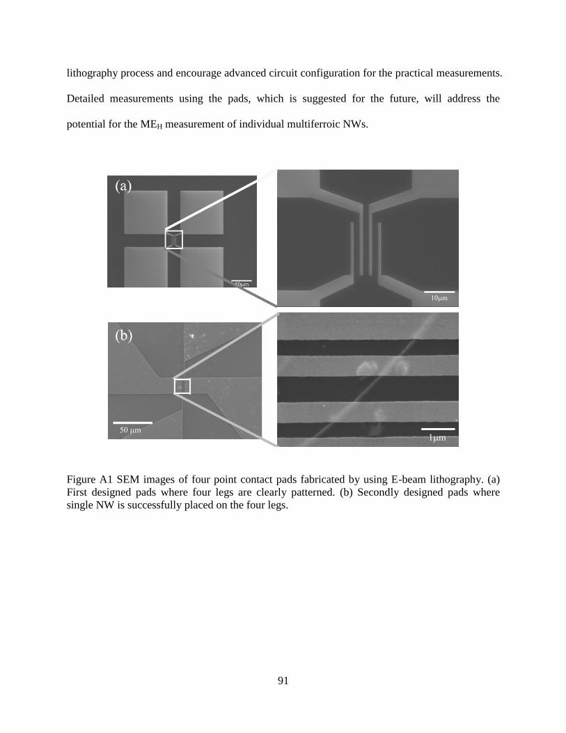
91
lithography process and encourage advanced circuit configuration for the practical measurements.
Detailed measurements using the pads, which is suggested for the future, will address the
potential for the MEH measurement of individual multiferroic NWs.
Figure A1 SEM images of four point contact pads fabricated by using E-beam lithography. (a)
First designed pads where four legs are clearly patterned. (b) Secondly designed pads where
single NW is successfully placed on the four legs.


![Study of Local Correlations of Magnetic and Multiferroic ... · phenomena and nanoscale inhomogeneities [6]. In the undoped compounds, where only Mn+3 ions are present, the cubic](https://cdn.vdocuments.us/doc/165x107/5f5f9eb147ee097db152cfe7/study-of-local-correlations-of-magnetic-and-multiferroic-phenomena-and-nanoscale.jpg)


