
ESE 570: Digital Integrated Circuits and VLSI Fundamentals
Lec 24: April 18, 2019 I/O Circuits, Inductive Noise
Penn ESE 570 Spring 2019 – Khanna

Lecture Outline
! Packaging ! Variation and Testing ! I/O Circuits ! Inductive Noise
2 Penn ESE 570 Spring 2019 – Khanna
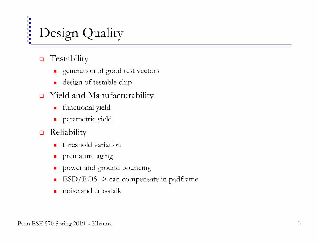
Design Quality
! Testability " generation of good test vectors " design of testable chip
! Yield and Manufacturability " functional yield " parametric yield
! Reliability " threshold variation " premature aging " power and ground bouncing " ESD/EOS -> can compensate in padframe " noise and crosstalk
3 Penn ESE 570 Spring 2019 - Khanna

Packaging Technology
! Include important package related parasitics in the chip design and simulation " Package VDD and GND planes
" On-chip VDD and GND busses
" Bond wire lengths " On-chip inductive effects
" Thermal resistance " Temp rise due to on-chip power dissipation
" Package cost
Penn ESE 570 Spring 2019 - Khanna
4
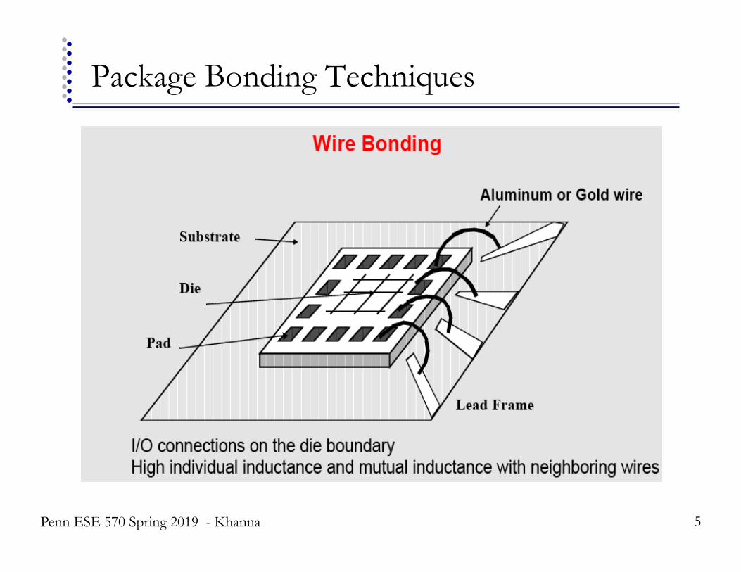
Package Bonding Techniques
5 Penn ESE 570 Spring 2019 - Khanna

Parasitics in an Electronic Package
6
PCB Transmission Line
PCB Ground Plane PCB Vias
Wire Bond Package Body
Die Paddle
Penn ESE 570 Spring 2019 - Khanna

Summary of Package Types
7

Variation and Testing

Modeling Process Variations
9
+
+
+
Penn ESE 570 Spring 2019 – Khanna

Parametric Yield
10
= = =
=
Penn ESE 570 Spring 2019 – Khanna

Parametric Yield
11
mτp = 0.184 ns στp = 0.023 ns
Penn ESE 570 Spring 2019 – Khanna
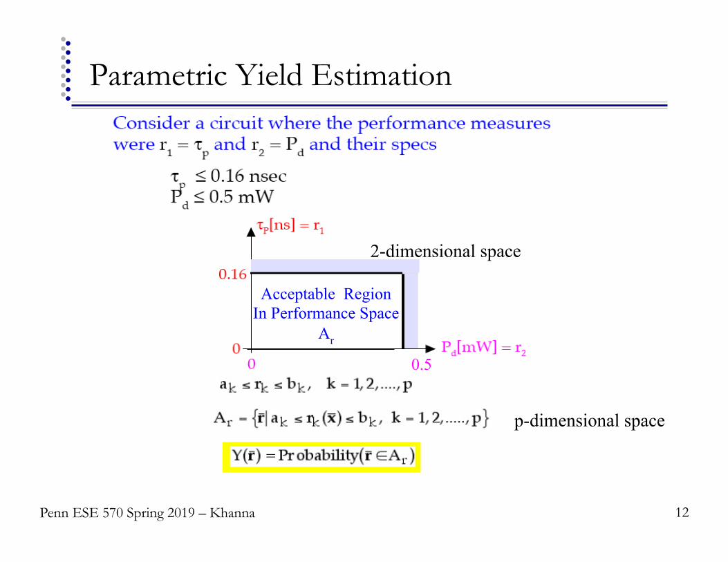
Parametric Yield Estimation
12
p-dimensional space
2-dimensional space
=
0.5
Acceptable Region In Performance Space
Ar
Penn ESE 570 Spring 2019 – Khanna

Parametric Yield Estimation
13
p-dimensional space
2-dimensional space Probability density functions (PDFs) for rk are usually not known specifically.
=
0.5
Parametric yield is a scalar, deterministic quantity that is difficult to evaluate.
Acceptable Region In Performance Space
Ar
Penn ESE 570 Spring 2019 – Khanna
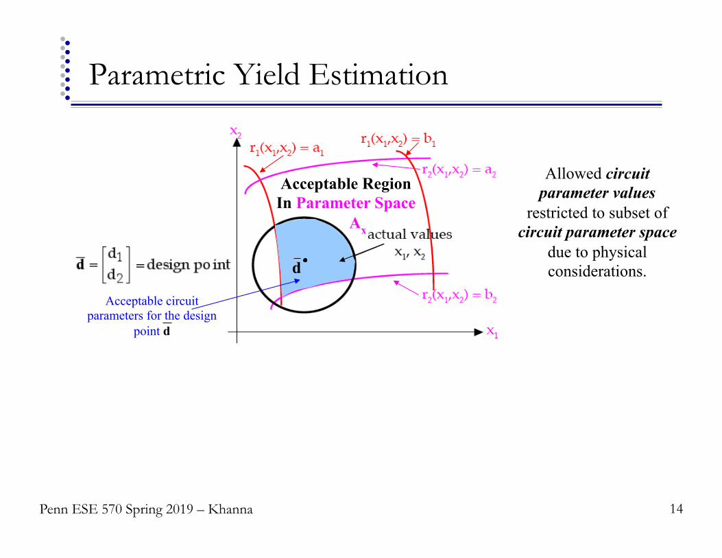
Parametric Yield Estimation
14
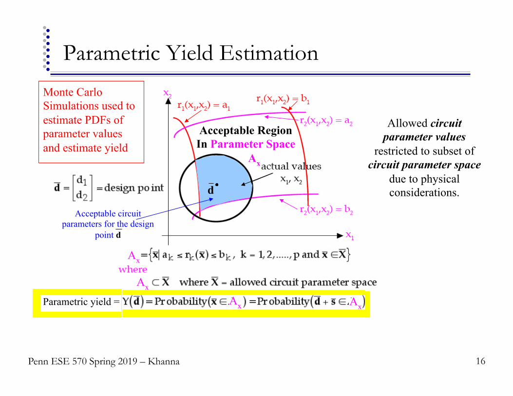
Allowed circuit parameter values
restricted to subset of circuit parameter space
due to physical considerations.
Acceptable Region In Parameter Space
Ax
d = =
=
= =
Ax
Ax
Ax Ax
Acceptable circuit parameters for the design
point d
Parametric yield =
Penn ESE 570 Spring 2019 – Khanna

Parametric Yield Estimation
15
Allowed circuit parameter values
restricted to subset of circuit parameter space
due to physical considerations.
Acceptable Region In Parameter Space
Ax
d = =
=
= =
Ax
Ax
Ax Ax
Acceptable circuit parameters for the design
point d
Parametric yield =
Penn ESE 570 Spring 2019 – Khanna
Parametric Yield Estimation
16
Allowed circuit parameter values
restricted to subset of circuit parameter space
due to physical considerations.
Acceptable Region In Parameter Space
Ax
d = =
=
=
Ax
Ax
Ax Ax
Acceptable circuit parameters for the design
point d
Parametric yield =
Monte Carlo Simulations used to estimate PDFs of parameter values and estimate yield
=
Penn ESE 570 Spring 2019 – Khanna

Manufacturing Process
17
Test dies on wafer Test packaged
parts
Penn ESE 570 Spring 2019 – Khanna

Manufacturing Tests
! Characterization Testing " Used to characterize devices and performed through
production life to improve the process, hence yield
! Production testing " Factory testing of all manufactured chips for parametric
faults and for random defects. " The test patterns may not cover all possible functions and
data patterns but must have a high fault coverage of modeled faults.
" The main driver is cost, since every device must be tested. Test time must be absolutely minimized.
" Only a go/no-go decision is made.
18 Penn ESE 570 Spring 2019 – Khanna
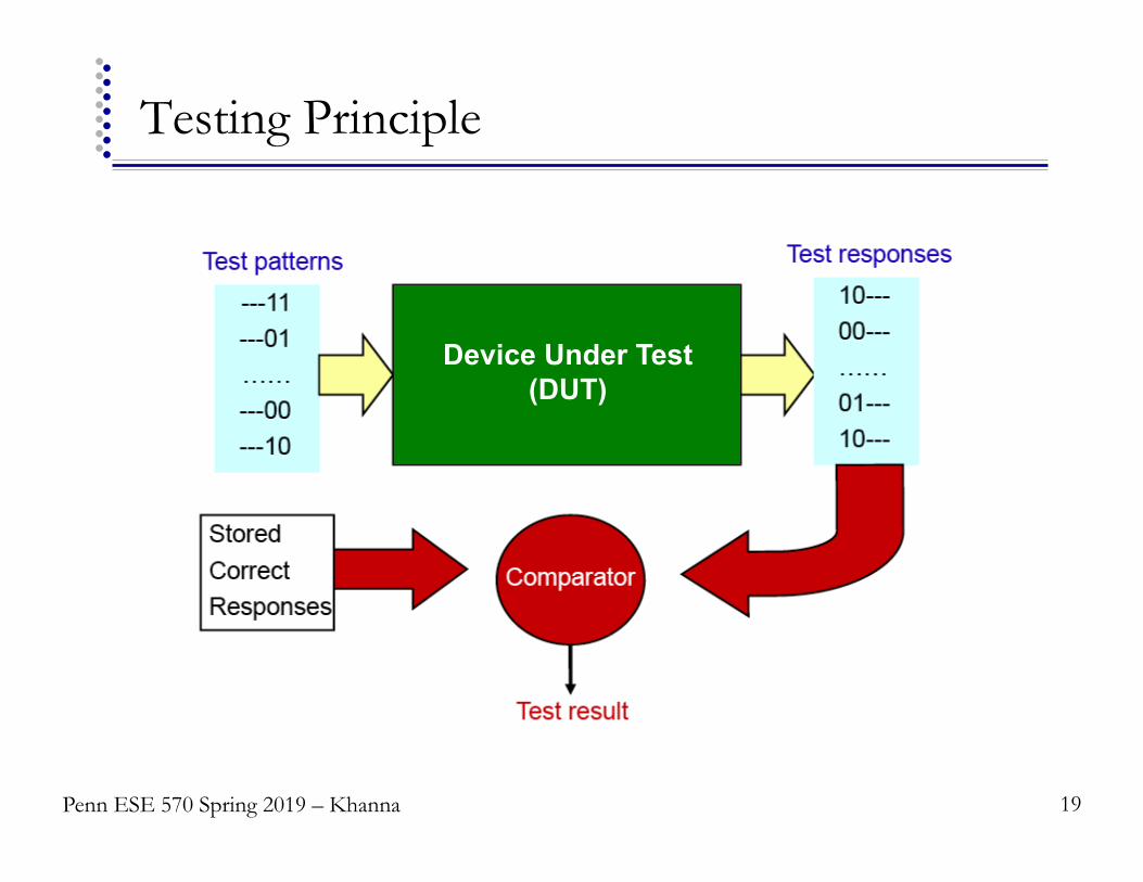
Testing Principle
19
Kenneth R. Laker, University of Pennsylvania,
updated 27Apr15
Device Under Test (DUT)
Penn ESE 570 Spring 2019 – Khanna

Observability & Controllability
! Observability: measure of the ease of observing a node by watching external output pins of the chip
! Controllability: measure of the ease of forcing a node to 0 or 1 by driving input pins of the chip
! Good observability and controllability reduces number of
test vectors required for manufacturing test " Reduces the cost of testing " Motivates design-for-test
20 Penn ESE 570 Spring 2019 – Khanna
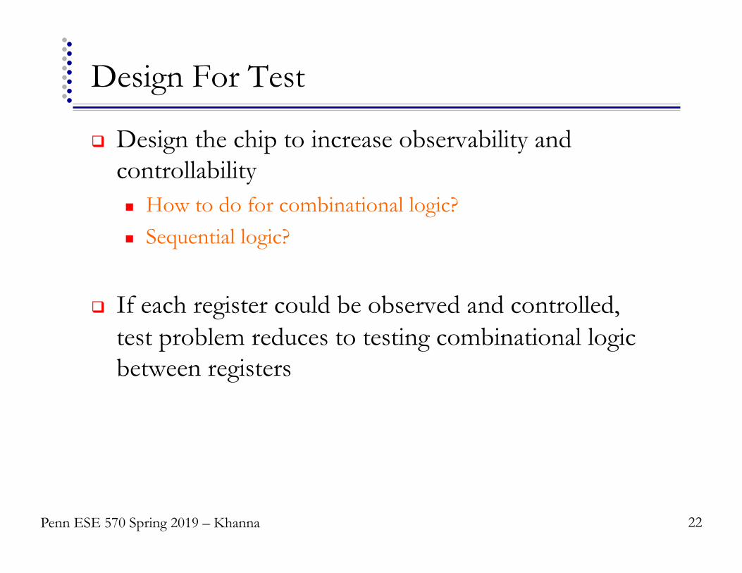
Design For Test
! Design the chip to increase observability and controllability " How to do for combinational logic? " Sequential logic?
21
Kenneth R. Laker, University of Pennsylvania,
updated 27Apr15
Penn ESE 570 Spring 2019 – Khanna
Design For Test
! Design the chip to increase observability and controllability " How to do for combinational logic? " Sequential logic?
! If each register could be observed and controlled, test problem reduces to testing combinational logic between registers
22
Kenneth R. Laker, University of Pennsylvania,
updated 27Apr15
Penn ESE 570 Spring 2019 – Khanna

Scan Based Testing
23
NORMAL TEST
! Scan test is to obtain control and observability for registers (eg. FFs) " It reduces sequential Test Pattern Generation circuits (TPG) to combinational TPG
circuits
! With Scan, a synchronous sequential circuit works in two modes. " Normal mode and Test mode:
! In test mode, all FFs are configured as shift registers, with Scan-in and Scan-out
Penn ESE 570 Spring 2019 – Khanna
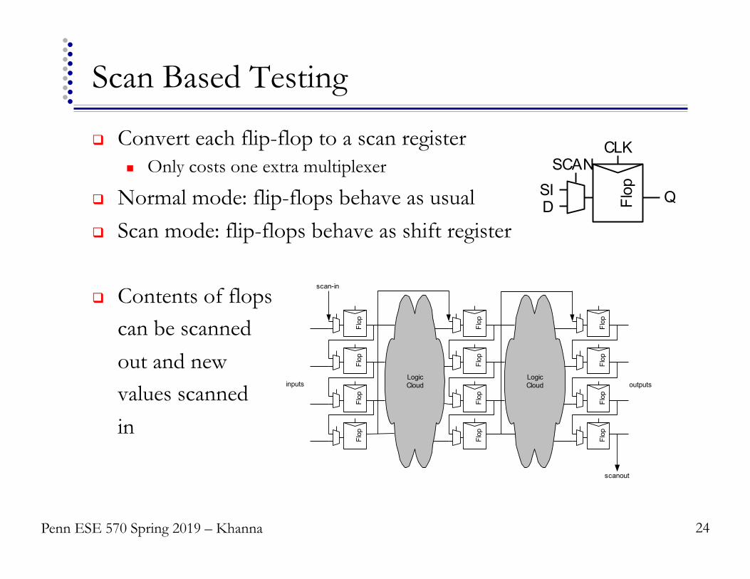
Scan Based Testing ! Convert each flip-flop to a scan register
" Only costs one extra multiplexer
! Normal mode: flip-flops behave as usual ! Scan mode: flip-flops behave as shift register
! Contents of flops can be scanned out and new values scanned in
Flop QD
CLK
SISCAN
scan out
scan-in
inputs outputs
Flop
Flop
Flop
Flop
Flop
Flop
Flop
Flop
Flop
Flop
Flop
Flop
LogicCloud
LogicCloud
Penn ESE 570 Spring 2019 – Khanna
24
I(nput)/O(utput) Circuits
Penn ESE 570 Spring 2019 – Khanna
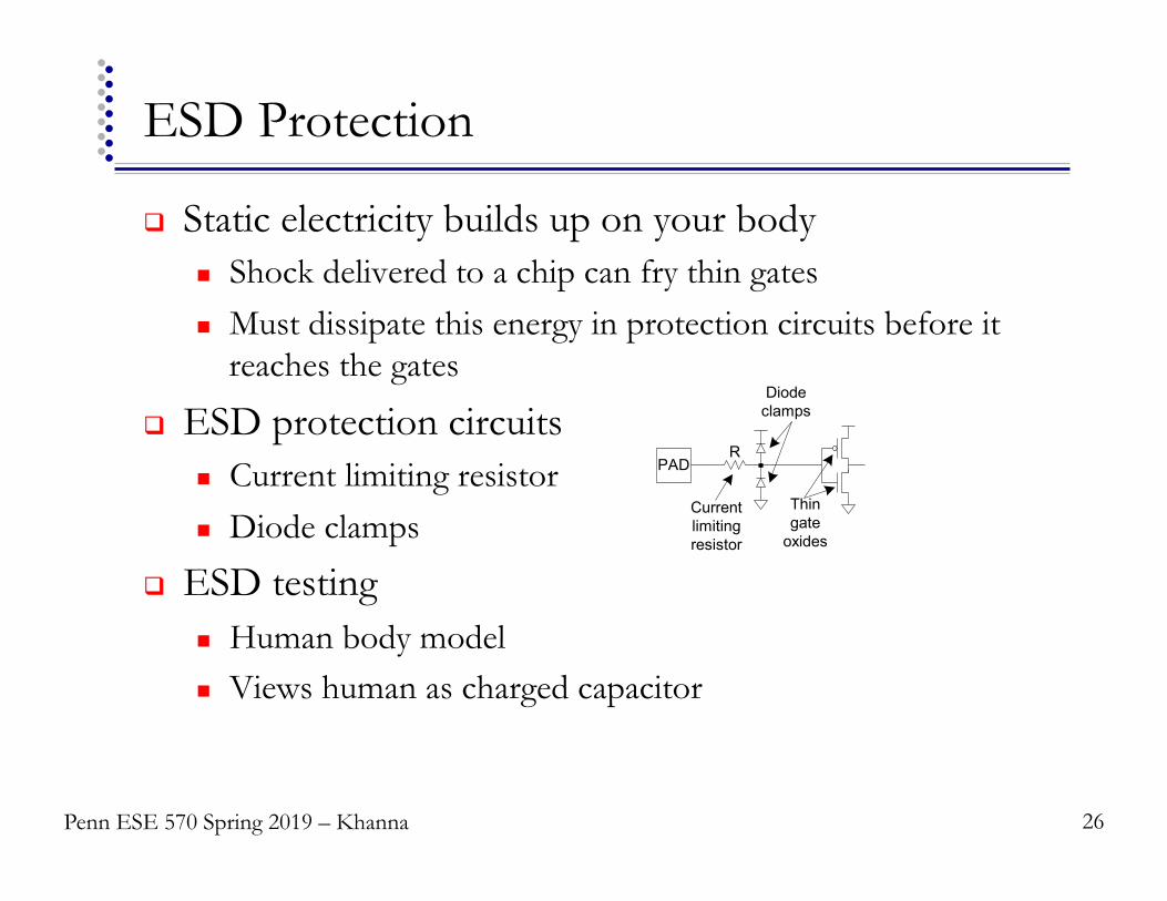
ESD Protection
! Static electricity builds up on your body " Shock delivered to a chip can fry thin gates " Must dissipate this energy in protection circuits before it
reaches the gates
! ESD protection circuits " Current limiting resistor " Diode clamps
! ESD testing " Human body model " Views human as charged capacitor
PADR
Diodeclamps
Thingateoxides
Currentlimitingresistor
Penn ESE 570 Spring 2019 – Khanna
26

ESD Protection
27
Kenneth R. Laker, University of Pennsylvania,
updated 6Apr15
Machine Model (MM) Human Body Model (HBM)
Electrostatic charge builds up and then discharges when a low-resistance path becomes available.
Penn ESE 570 Spring 2019 – Khanna

Lumped Circuit model of HBM and MM
28
After exposure to the ESD waveform, a failed IC exhibits latch-up or fails one or more data sheet specifications.
Penn ESE 570 Spring 2019 – Khanna

ESD Protection Network
29
Kenneth R. Laker, University of Pennsylvania,
updated 6Apr15
VDD
Penn ESE 570 Spring 2019 – Khanna

Input Pad with Tristate Buffer
30
Kenneth R. Laker, University of Pennsylvania,
updated 6Apr15
TB
Penn ESE 570 Spring 2019 – Khanna

Output Pads
31
Kenneth R. Laker, University of Pennsylvania,
updated 6Apr15
CK
CK D P N Z 1 1 0 0 1 = D 1 0 1 1 0 = D 0 x 1 0 HIGH Z
Penn ESE 570 Spring 2019 – Khanna

Output Pads
32
Kenneth R. Laker, University of Pennsylvania,
updated 6Apr15
MN1
MN2
MP2
MP1
CK = 0 => MN2 & MP2 OFF => Z = HIGH Z CK = 1 => MN2 & MP2 ON => Z = D
Penn ESE 570 Spring 2019 – Khanna

Bidirectional Pads
! Combine input and output pad ! Need tristate driver on output
" Use enable signal to set direction " Optimized tristate avoids huge series transistors
PAD
Din
Dout
En
33
Penn ESE 570 Spring 2019 – Khanna

I/O Pad
34
! 0.6 µm three-metal process " Similar I/O drivers " Big driver transistors
provide ESD protection " Guard rings around driver
Out
En
Out
PAD
In
In_bIn_unbuffered
100
100
52
3030
52
Enb Enbuf
Enb
Enbuf
Driver drain diodes
Penn ESE 570 Spring 2019 – Khanna
Inductance of Wire
35 Penn ESE 570 Spring 2019 – Khanna

Inductance: Wire over Ground Plane
36
€
L ≈ l µ0µrhw
#
$ %
&
' (
C = εrε0Ad= εrε0
wlh
Penn ESE 570 Spring 2019 – Khanna

37
C 'L ' = εµ
L ' = εµC '
C’ and L’ per unit length
C ' = εrε0wh
L ' ≈ µ0µrhw
"
#$
%
&'
Inductance: Wire over Ground Plane
Penn ESE 570 Spring 2019 – Khanna

On Chip Inductance
! Cwire = 0.16 pF (for the 1mm) ! Cwire = 0.16nF/m
! Permeability µ0≈ µSi02=12.6×10⁻⁷H/m
! Permitivity εox=3.5×10⁻¹¹F/m
38
L ' = εµC '
Penn ESE 570 Spring 2019 – Khanna

On Chip Inductance
! Cwire = 0.16 pF (for the 1mm) ! Cwire = 0.16nF/m
! Permeability µ0≈ µSi02=12.6×10⁻⁷H/m
! Permitivity εox=3.5×10⁻¹¹F/m ! 276 pH (for 1 mm)
39
L ' = εµC '
Penn ESE 570 Spring 2019 – Khanna

Inductors
! Bond pads/wires ! Package leads ! Long wire runs ! Cables
40
Src: http://en.wikipedia.org/wiki/File:Wirebonding2.svg
Penn ESE 570 Spring 2019 – Khanna

Parasitics in an Electronic Package
41
Kenneth R. Laker, University of Pennsylvania,
updated 6Apr15
PCB Transmission Line
PCB Ground Plane PCB Vias
Wire Bond Package Body
Die Paddle
Penn ESE 570 Spring 2019 - Khanna

Inductive Noise
Penn ESE 570 Spring 2019 – Khanna

LC Response
! What happens here?
43
V2
V2 = A+Bejωt
ω =1LC
V2 =V +Bej 1
CL
!
"##
$
%&&t
Penn ESE 570 Spring 2019 – Khanna

LC Response
! What happens here?
44
V2
V2 = A+Bejωt
ω =1LC
V2 =V +Bej 1
CL
!
"##
$
%&&t
Penn ESE 570 Spring 2019 – Khanna

Response?
45
V2
Penn ESE 570 Spring 2019 – Khanna

Decay Oscillation V2
RLC Response
46
! For what R does this circuit oscillate?
V2 =VS +Be−R2L
"
#$
%
&'te
j 1LC
−R2L"
#$
%
&'2"
#
$$
%
&
''t
Penn ESE 570 Spring 2019 – Khanna
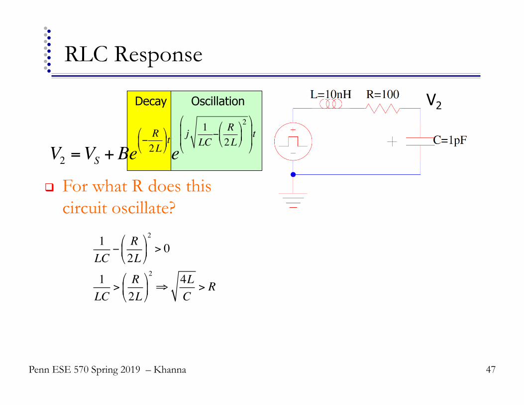
Decay Oscillation V2
RLC Response
47
! For what R does this circuit oscillate?
1LC
−R2L"
#$
%
&'2
> 0
1LC
>R2L"
#$
%
&'2
⇒4LC
> R
V2 =VS +Be−R2L
"
#$
%
&'te
j 1LC
−R2L"
#$
%
&'2"
#
$$
%
&
''t
Penn ESE 570 Spring 2019 – Khanna

RLC Response (R=100)
48 Penn ESE 570 Spring 2019 – Khanna

RLC Response
49 Penn ESE 570 Spring 2019 – Khanna

Where Inductive Noise Arises
50 Penn ESE 570 Spring 2019 – Khanna

Signal Path
51 Penn ESE 570 Spring 2019 – Khanna
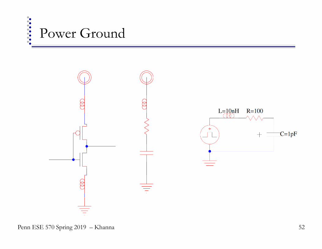
Power Ground
52 Penn ESE 570 Spring 2019 – Khanna

Power Ground
53 Penn ESE 570 Spring 2019 – Khanna
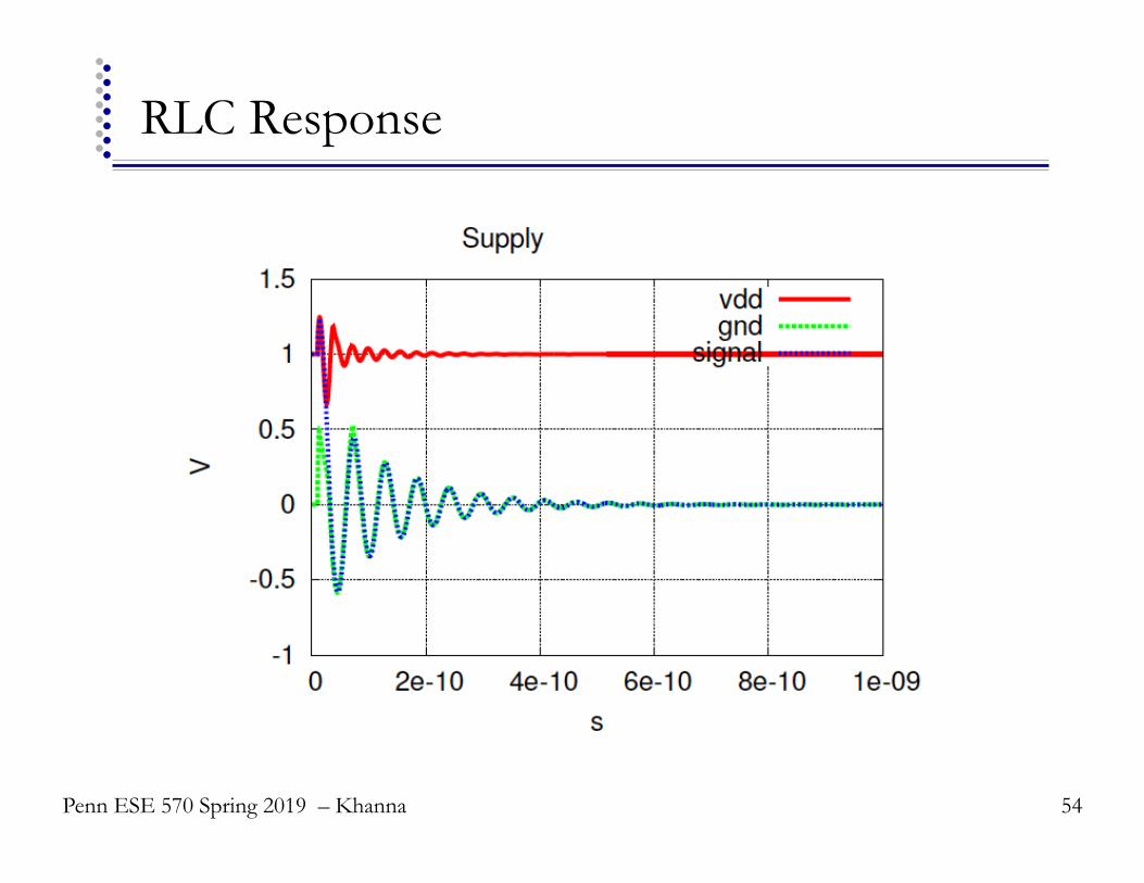
RLC Response
54 Penn ESE 570 Spring 2019 – Khanna

How to Improve Inductive Noise
55 Penn ESE 570 Spring 2019 – Khanna
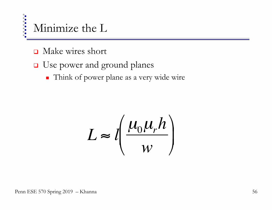
Minimize the L
! Make wires short ! Use power and ground planes
" Think of power plane as a very wide wire
56
€
L ≈ l µ0µrhw
#
$ %
&
' (
Penn ESE 570 Spring 2019 – Khanna

Flip Chip, Area IO
57
http://www.izm.fraunhofer.de/en/abteilungen/high_density_interconnectwaferlevelpackaging/arbeitsgebiete/arbeitsgebiet1.html
Penn ESE 570 Spring 2019 – Khanna

Add Good C’s
! Bypass Capacitors – inside the inductances " On board " On package " On chip
58 Penn ESE 570 Spring 2019 – Khanna

Bypass Capacitor Example
59 Penn ESE 570 Spring 2019 – Khanna

Bypass Capacitor Example
60
No bypass cap No package inductance
package inductance w/ bypass cap Penn ESE 570 Spring 2019 – Khanna

Bypassed Supplies (@ transistor)
61 Penn ESE 570 Spring 2019 – Khanna
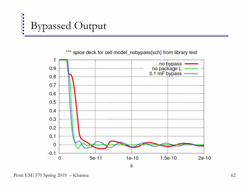
Bypassed Output
62 Penn ESE 570 Spring 2019 – Khanna

Idea
! Observability and Controlability reduce cost of testing and motivates design-for-test
! I/O circuits attempt to interact with and isolate from external sources " ESD protection, level shifting " High impedence output
! Inductive noise " Originates in signal paths and supplies " Minimize wires when possible and add bypass capacitors
63 Penn ESE 570 Spring 2019 – Khanna

Admin
! Final Project " Design memory (SRAM)
" EC for best figure of merits (FOM = Area*Power*Delay2)
" Due 4/30 (last day of class) " Everyone gets an extension until 5/7 " Absolutely doable by 2 people by 4/30
64 Penn ESE 570 Spring 2019 – Khanna


