
Energy Bands in Semiconductors & Carrier Concentrations
Dr. Mohammad Aminul IslamAssistant Professor
Dept. of EEEInternational Islamic University Chittagong
Chapter 1

OutlinesoMetals, Semiconductor and Insulators
oAccording to the bonding energyoAccording to the energy bandgap
oEnergy bandgapsoDirect and indirect bandgap semiconductor
oColors in SemiconductoroAbsorption
oDirect and indirect absorption in semiconductoro Photoconductivity
M A Islam, EEE, IIUC

Bonding Forces & Energy Bands in Solids
• Isolated Atoms: conductor • Solid Materials: conduction depends on the bonding force
3rd Band2nd Band
1st Band
Core
M A Islam, EEE, IIUC

Bonding Forces in Solids
• Na (Z=11) [Ne]3s1
• Cl (Z=17) [Ne]3s1 3p5
Na+ Cl_
M A Islam, EEE, IIUC

Bonding Forces in Solids
e_
Na+
M A Islam, EEE, IIUC

3-1-1. Bonding Forces in Solids
M A Islam, EEE, IIUC
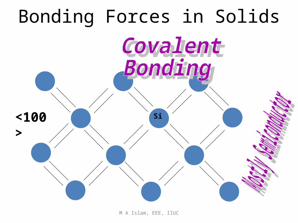
Bonding Forces in Solids
Si<100>
M A Islam, EEE, IIUC

Metals, Semiconductors & Insulators
• The difference bet-ween insulators and semiconductor mat-erials lies in the size of the band gap Eg, which is much small-er in semiconductors than in insulators.
Insulator Semiconductor
Filled
Filled
Empty
Empty
Eg
Eg
M A Islam, EEE, IIUC

Metals, Semiconductors & Insulators
Metal
Filled
Partially Filled
Overlap
In metals the bands either overlap or are only partially filled. Thus electrons and empty energy states
Metal
are intermixed with-in the bands so that electrons can move freely under the infl-uence of an electric field.M A Islam, EEE, IIUC

• energy gap or bandgap, is an energy range in a solid where no electron states can exist.
• A semiconductor is a material with a small but non-zero band gap that behaves as an insulator at absolute zero but allows thermal excitation of electrons into its conduction band at temperatures that are below its melting point.
• In contrast, a material with a large band gap is an insulator.
• In conductors, the valence and conduction bands may overlap, so they may not have a band gap.
Energy Band gap & Solid Materials
M A Islam, EEE, IIUC

Visual Appearance of Insulators, Metals, & Semiconductors
• A material’s appearance & color depend on the interaction between light with the electron configuration of the material.
NormallyHigh resistivity materials (Insulators) are Transparent
High conductivity materials (Metals) have a “Metallic
Luster” & are Opaque
Semiconductors can be opaque or transparentThis & their color depend on the material band gap
• For semiconductors the energy band diagram can explain the appearance of the material in terms of both luster & color.
M A Islam, EEE, IIUC

Group Material Symbol Band gap (eV) @ 302K
IV Diamond C 5.5IV Silicon Si 1.11IV Germanium Ge 0.67III–V Gallium(III) nitride GaN 3.4III–V Gallium(III) phosphide GaP 2.26III–V Gallium(III) arsenide GaAs 1.43
IV–V Silicon nitride Si3N4 5
IV–VI Lead(II) sulfide PbS 0.37
IV–VI Silicon dioxide SiO2 9
Copper(I) oxide Cu2O 2.1
List of band gaps of semiconductor materials.
M A Islam, EEE, IIUC

Semiconductor Materialso Element : Si, Geo IV compounds : SiC, SiGeo III-V compounds: AIP, AlAs, AlSb, GaN,GaP, GaAs,
GaSb, InP, InAs, InSbo II-VI: SnS, ZnSe, ZnTe, CdS, CdSe, CdTeo LED(GaN, GaP, GaAs), Three-elements(GaAsP,
InGaAsP), Fluorescent(II-VI, ZnS), Light detector(InSb, CdSe), PbTe, HgCdTe, Si, Ge)
II III IV V VI
BBoron
CCarbon
NNitrogen
OOxygen
AlAluminum
SiSilicon
PPhosphorus
SSulfur
ZnZinc
GaGalium
GeGermanium
AsArsenic
SeSelenium
CdCadmium
InIndium
SnTin
SbAntimony
TeTellurium M A Islam, EEE, IIUC

Direct & Indirect Semiconductors
In a direct band gap semiconductor, the top of the valence band and the bottom of the conduction band occur at the same value of momentum, as in the schematic below.
Direct Band Gap
M A Islam, EEE, IIUC

3-1-4. Direct & Indirect Semiconductors
Indirect Band GapIn an indirect band gap semiconductor, the maximum energy of the valence band occurs at a different value of momentum when comparing with the minimum in the conduction band.
M A Islam, EEE, IIUC

3-1-4. Direct & Indirect Semiconductors
Eg=hνEg Et
k k
EE
Direct IndirectExample 3-1
M A Islam, EEE, IIUC

Direct & Indirect SemiconductorsFor an indirect-band gap material; the minimum of the CB and maximum of the VB lie at different k-values.
When an e- and hole recombine in an indirect-band gap s/c, phonons must be involved to conserve momentum.
In indirect band gap semiconductors may have iso electronic impurity states or Defect state which are direct, and therefore the recombination from these states may also be radiative.
Direct band gap semiconductors are capable of photon emission, by radiative recombination,but indirect semiconductors have a low probability of radiative recombination.
M A Islam, EEE, IIUC

• Recall: Semiconductor Bandgaps Eg are usually
in the range: 0 < Eg < 3 eV(up to 6 eV if diamond is included)
• Also, at equilibrium, at temperature T = 0, the valence band is full & the
conduction band is empty.• Now, consider what happens if electromagnetic
radiation (“light”) is shined on the material.
• In the photon representation of this radiationIf hν Eg, some electrons can be promoted to the conduction band leaving some holes in the
valence band. M A Islam, EEE, IIUC

Colors of Semiconductors
I B G Y O R
EEvisvis= 1.8eV = 1.8eV 3.1eV 3.1eV
If the Photon Energy is Evis > Egap Photons will be absorbed
If the Photon Energy is Evis < Egap Photons will transmitted
If the Photon Energy is in the range of Egap those with higher energy than Egap will be absorbed.
We see the color of the light being transmitted.If all colors are transmitted the light is White
M A Islam, EEE, IIUC
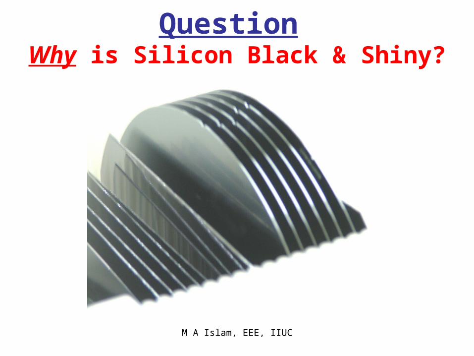
Question Why is Silicon Black & Shiny?
M A Islam, EEE, IIUC

To Answer This:• We need to know that the energy gap of Si is:
Egap = 1.2eV • We also need to know that, for visible light, the
photon energy is in the range:
Evis ~ 1.8 – 3.1eVSo, for Silicon, Evis is larger than Egap
• So, all visible light will be absorbed & Silicon appears black
So, why is Si shiny?• The answer is somewhat subtle: Significant photon
absorption occurs in silicon, because there are a significant
number of electrons in the conduction band. These electrons are delocalized. They scatter photons. M A Islam, EEE, IIUC

Why is GaP Yellow?
• We need to know that the energy gap of GaP is:
Egap = 2.26 eV This is equivalent to a
Photon of Wavelength = 549 nm. • So photons with E = h > 2.26 eV (i.e. green, blue,
violet) are absorbed.• Also photons with E = h < 2.26eV (i.e. yellow,
orange, red) are transmitted.• Also, the sensitivity of the human eye is greater for yellow
than for red, so
GaP Appears Yellow/Orange.
To Answer This:
M A Islam, EEE, IIUC

Why is Glass Transparent?• Glass is an insulator (with a huge band gap). Its is difficult
for electrons to jump across a big energy gap: Egap >> 5eV
Egap >> E(visible light) ~ 2.7- 1.6eV• All colored photons are transmitted, with no absorption, hence the
light is transmitted & the material is transparent.• Define transmission & absorption by
Lambert’s Law: I = Ioexp(-x)Io = incident beam intensity, I = transmitted beam intensityx = distance of light penetration into material from a surface
total linear absorption coefficient (m-1) takes into account the loss of intensity from scattering centers & absorption centers. approaches zero for a pure insulator. M A Islam, EEE, IIUC
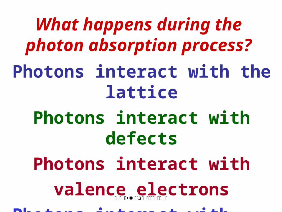
What happens during the photon absorption process?
Photons interact with the lattice
Photons interact with defects
Photons interact with
valence electrons
Photons interact with …..

AbsorptionAn Important Phenomena in the Description of
the Optical Properties of Semiconductors• Light (electromagnetic radiation) interacts with
the electronic structure of the material.
The Initial Interaction is Absorption• This occurs because valence electrons on the
surface of a material absorb the photon energy & move to higher-energy states.
• The degree of absorption depends, among many other things, on the number of valence electrons capable of receiving the photon energy. M A Islam, EEE, IIUC
• The photon-electron interaction process obviously depends strongly on the photon energy.
• Lower Energy Photons interact principally by ionization or excitation of the solid’s valence electrons.
• Low Energy Photons (< 10 eV) are in the infrared (IR), visible & ultraviolet (UV) in the EM spectrum.
• High Energy Photons (> 104 eV) are in the X-Ray & Gamma Ray region of the EM spectrum.
• The minimum photon energy to excite and/or ionize a solid’s valence electrons is called the
Absorption Edge orAbsorption Threshold.
M A Islam, EEE, IIUC

Valence Band – Conduction Band Absorption(Band to Band Absorption)
Conduction Band, EC
Valence Band, EV
Egaph = Ephoton
M A Islam, EEE, IIUC

Conduction Band, EC
Valence Band, EV
Egaph = Ephoton
This process obviously requires that the minimum energy of a photon to initiate an electron transition must satisfy
EC - EV = h = Egap
Valence Band – Conduction Band Absorption(Band to Band Absorption)
M A Islam, EEE, IIUC

Valence Band – Conduction Band Absorption(Band to Band Absorption)
Conduction Band, EC
Valence Band, EV
Egaph = Ephoton
This process obviously requires that the minimum energy of a photon to initiate an electron transition must satisfy
EC - EV = h = Egap
If h > Egap then obviously a transition can happen. Electrons are then excited to the
conduction band.
M A Islam, EEE, IIUC
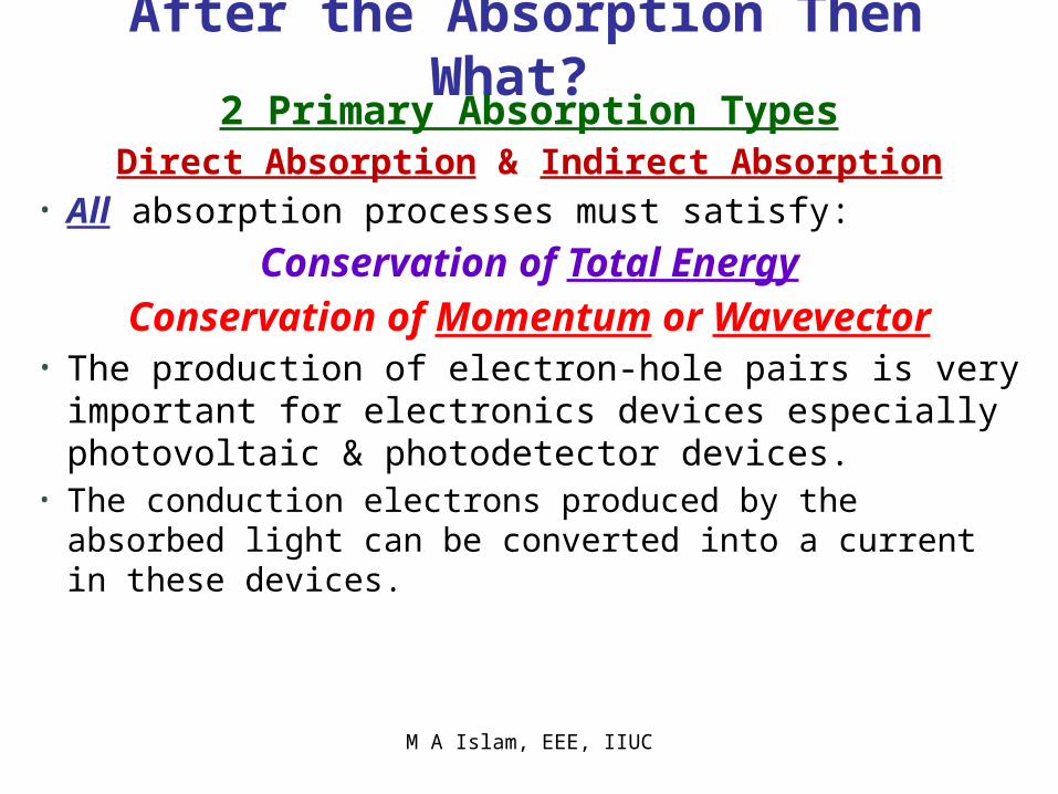
After the Absorption Then What? 2 Primary Absorption Types
Direct Absorption & Indirect Absorption• All absorption processes must satisfy:
Conservation of Total EnergyConservation of Momentum or Wavevector
• The production of electron-hole pairs is very important for electronics devices especially photovoltaic & photodetector devices.
• The conduction electrons produced by the absorbed light can be converted into a current in these devices.
M A Islam, EEE, IIUC
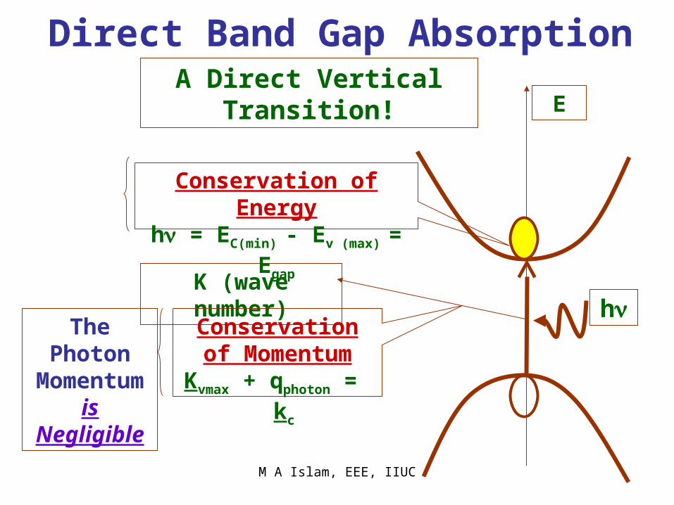
Direct Band Gap Absorption
K (wave number)h
Conservation of Energyh = EC(min) - Ev (max) = Egap
Conservation of Momentum
Kvmax + qphoton = kc
EA Direct Vertical
Transition!
The Photon Momentum is Negligible
M A Islam, EEE, IIUC
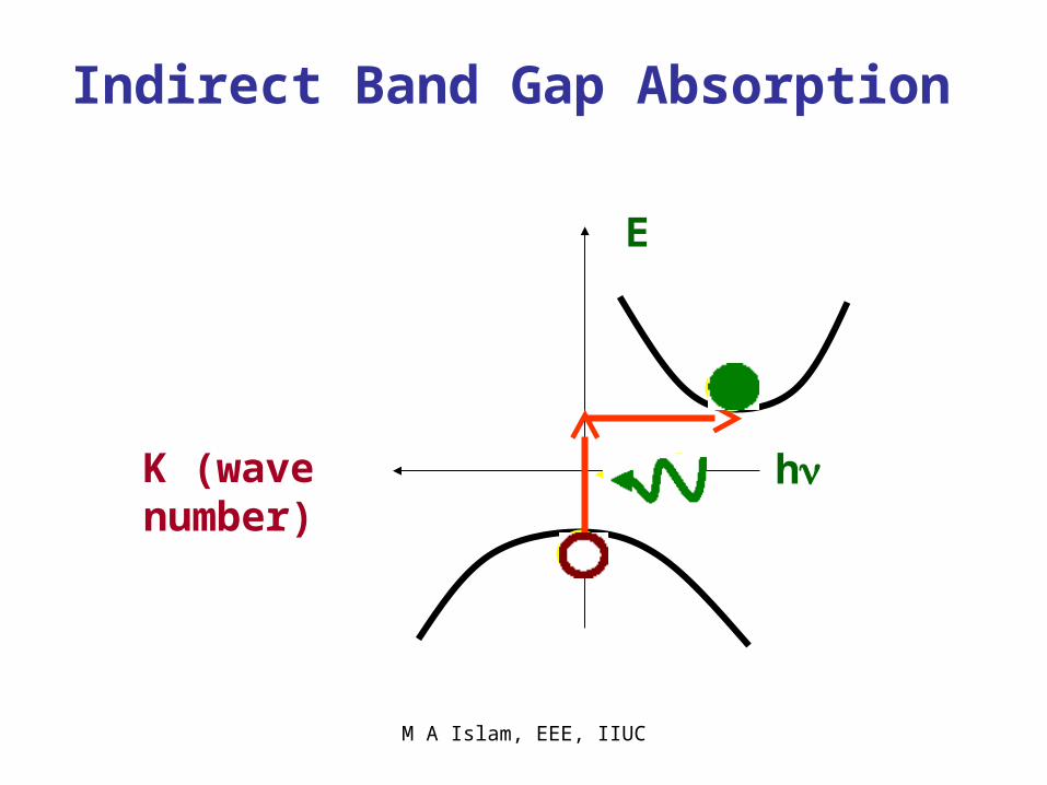
Indirect Band Gap Absorption
E
K (wave number) h
M A Islam, EEE, IIUC
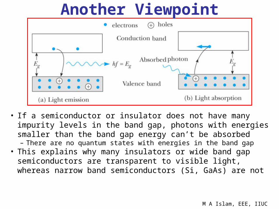
• If a semiconductor or insulator does not have many impurity levels in the band gap, photons with energies smaller than the band gap energy can’t be absorbed– There are no quantum states with energies in the band gap
• This explains why many insulators or wide band gap semiconductors are transparent to visible light, whereas narrow band semiconductors (Si, GaAs) are not
Another Viewpoint
M A Islam, EEE, IIUC
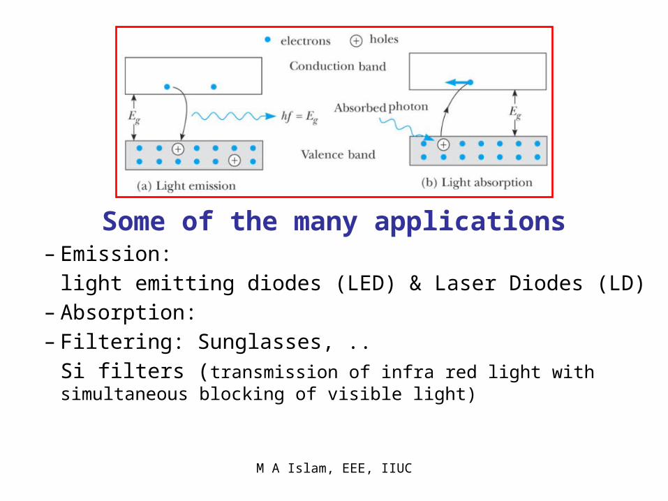
Some of the many applications– Emission:
light emitting diodes (LED) & Laser Diodes (LD)– Absorption: – Filtering: Sunglasses, ..
Si filters (transmission of infra red light with simultaneous blocking of visible light)
M A Islam, EEE, IIUC

• If there are many impurity levels the photons with energies smaller than the band gap energy can be absorbed, by exciting electrons or holes from these energy levels into the conduction or valence band, respectively– Example: Colored Diamonds
M A Islam, EEE, IIUC

Photoconductivity• Charge carriers (electrons or
holes or both) created in the corresponding bands by absorbed light can also participate in current flow, and thus should increase the current for a given applied voltage, i.e., the conductivity increases
• This effect is called Photoconductivity
• Want conductivity to be controlled by light. So want few carriers in dark → A semiconductor
• But want light to be absorbed, creating photoelectrons
• → Band gap of intrinsic photoconductors should be smaller than the energy of the photons that are absorbed
M A Islam, EEE, IIUC


![[ e„wËi †M‡RU ] · 0008 148542 tahmin wasif alam chittagong govt. high school chittagong sadar male 0009 148558 mohammad aiman aousaf hossain chittagong govt. high school chittagong](https://cdn.vdocuments.us/doc/165x107/5f3ca57371ed6164dd4c9a40/-eawi-amaru-0008-148542-tahmin-wasif-alam-chittagong-govt-high-school.jpg)


