
Abstract — The evolution of technology in the field of
power electronics has been very evident in recent years,
including the development of new semiconductors that are
prepared to operate in systems with high working voltage,
as in the case of ultra high voltage device.
On the other hand, there has also been a large
development in high-frequency transformers, in particular
ferromagnetic alloys that promote a high saturation flux
density, that means a high power density as well as lower
losses ensuring good efficiency of the transformer.
This paper proposes a high frequency power transformer
for applications in power systems, that is, beyond the
reduction / increase of voltage levels and galvanic isolation
garnished by the classic transformer, the proposed
transformer allows many other features such as: large
capacity control, lower volume of the transformer core,
good performance against voltage fluctuations.
This transformer is designated Solid State Transformer,
and it is composed of a Modular Matrix Converter, a Three
Phase Matrix Converter and High Frequency Transformer.
The SST allows to obtain a system of adjustable output
voltage under load, not only in amplitude but also in
frequency.
The Modular Matrix Converter was designed during the
course of the dissertation. In addition to being able to
operate in MV systems, it also enables the unsaturation of
the transformer.
Index Terms — Solid State Transformer; High Frequency
Transformer; Matrix Converter; Space Vector
Modulation; Voltage Regulator; Current Regulator
I. INTRODUCTION
owadays power transformers are essential devices in the
power distribution system. The widespread use of this
device has resulted in a cheap, efficient, reliable and mature
technology and any increase in performance are marginal and
come at great cost [1]. Despite their great utility, they present
some disadvantages such as [2]:
1. Bulky size and heavy weight
2. Transformer oil can be harmful when exposed to the
environment
3. Core saturation produces harmonics, which results in
large inrush currents
4. Unwanted characteristics on the input side, such as
voltage dips, are represented in output waveform
5. Sensitivity to the harmonics of the output current
6. Voltage regulation inefficient
In 1980, researcher James Brooks implemented the first
prototype of the SST. Due to major technological limitations at
the time he had little success. However, after a few years, the
concept of SST developed, with different architectures and
topologies, and in the last 10 years, the architecture and
topology of SST has been adapted to enable new applications,
especially in energy systems.
In recent years, interest in Solid State Transformers has
grown so much that in 2010 the SST technology was named by
MIT "Massachusetts" Institute of Technology ", as one of the
technologies greater relevance in future power distribution
systems. In recent years, many researchers have been studying
new applications of SST, resulting in different architectures and
topologies, which are associated with different applications [3].
VAC VACThree-phase Matrix
Converter
High Frequency Transformer
50/60Hz 50/60HzHigh Frequency> 1kHz
Modular Matrix Converter
Figure 1 – SST Concept
The Solid State Transformer (SST) provides an alternative to
the Low Frequency Transformer (LFT). The proposed SST is
presented in Figure 1 is based on one three phase High
Frequency Transformer supported by power electronic
converters. The input is connected with a Modular Matrix
Converter with an innovative feature that guarantees the non-
saturation of the HFT. Given the voltages applied to the SST,
and the limitations of the used semiconductor, has been
designed a modular matrix converter, which ensures that each
semiconductor support a small fraction of the maximum system
voltage. Thus, it is possible to ensure that the maximum voltage
applied to the semiconductor never exceeds the maximum
allowable values.
Electronic Power Transformer for Applications
in Power Systems
Electronic Power Transformer for Applications
in Power Systems
Pedro Miguel Costa Fernandes
Department of Electrical and Computer Engineering
Instituto Superior Técnico - Technical University of Lisbon, Portugal
Email: [email protected]
N

The output is connected with a three phase Matrix Converter
controlled by Space Vector Modulation (SVM).
II. SOLID STATE TRANSFORMER (SST)
A. Modular Matrix Converter
The modular matrix converter consists of single-phase
matrix converters in series, ensuring that the maximum voltage
applied to the semiconductors is compatible with existing
semiconductors in the market. Thus, it is possible to preserve
the proper operation thereof (Figure 3)
Figure 3 - Simplified scheme of the association in series of single-
phase matrix converters
B. Single-Phase Matrix Converter
The single-phase matrix converter consists of four
bidirectional switches fully controlled, allowing the
interconnection of two single-phase systems, one with
characteristics of voltage source and another with
characteristics of current source (Figure 4).
Assuming that the bidirectional semiconductor switches have
an ideal behaviour (zero voltage when they are ON, zero
leakage current when they are OFF and nearly zero switching
time), and each of the switches can be represented
mathematically by a variable 𝑆𝑘𝑗 which can take the value of
"1" if the switch is closed (ON) and the value of "0" if the switch
is open (OFF).
One can represent the state of the converter in a 2x2 matrix
(1).
S11
Va
Vb
Ia
Ib
S12
S21
S22
VA VB
IA IB
Figure 4 – Single-Phase Matrix Converter
Input Filter
Output FilterThree-phase Matrix Converter
Load
Modular Matrix Converter
High Frequency Transfomer
Figure 2 - Simplified schematic of the SST model

We must take into account compliance with the topological
constraints, implying that in each time step, each phase output
is only connected to one and only one input phase.
𝑺 = [𝑆11 𝑆12𝑆21 𝑆22
] (1)
In Table I are described four possible states, with the
respective correlations between the electrical variable
combinations.
Table I – Possible switch combination for a Single-Phase
Converter
Stat
e
Si11 Si12 Si21 Si22 VA VB iA iB
1 1 0 0 1 Va Vb IA IB
2 0 1 1 0 Vb Va IB IA
3 1 0 1 0 Va Va 0 0
4 0 1 0 1 Vb Vb 0 0
C. Three Phase Matrix Converter
The three-phase Matrix Converter, which is represented in
Figure 5. It consists of nine controlled bidirectional switches
making a 3x3 matrix (2) that allows a connection between two
three-phase systems; the input with voltage source
characteristics and the output system with characteristics of
current source. These converters allow direct AC-AC
conversion, without an intermediate but with a high efficiency
guaranty.
By assuming ideal semiconductors, each switch can be
mathematical represented by 𝑺𝒌𝒋 = 1, 𝑘 ∈ {1,2,3}, a binary
variable with two possible states: “𝑺𝒌𝒋 = 1” if the switch is ON,
and “𝑺𝒌𝒋 = 0” if it OFF. Due to electrical limitations of the MC
topology, each line of the matrix can only have one switch “ON.
(2)
𝑺 = [
𝑆11 𝑆12 𝑆13𝑆21 𝑆22 𝑆23𝑆31 𝑆32 𝑆33
] ∑𝑺𝑘𝑗 = 1, 𝑘 ∈ {1,2,3}
3
𝑗=1
(2)
S11
Va
Vb
Vc
Ia
Ib
Ic
S12
S13
S21 S31
S22 S32
S13 S13
IA IB IC
VA VB VC Figure 5 – Three-Phase Matrix Converter
The S matrix represents the states of the switches and enables
a mathematical correlation between the line-to-neutral output
voltages VA, VB, VC and the line-to-neutral input voltages Va,
Vb, Vc. Still, the transpose of matrix S correlates the input
currents ia, ib, ic with the output currents (3).
[
𝑉𝐴𝑉𝐵𝑉𝐶
] = 𝑺 [
𝑉𝑎𝑉𝑏𝑉𝐶
] [
𝐼𝑎𝐼𝑏𝐼𝑐
] = 𝑺𝑻 [
𝐼𝐴𝐼𝐵𝐼𝐶
] (3)
Finally, the three-phase Matrix Converter has now 27 possible
combinations to represent the input currents and output
voltages.
D. SVM – Space Vector Modulation
SVM approach, including Indirect SVM and Direct SVM
proposed in [4] and [5] were often used in MC for it’s
appropriate in operation. Conventional SVM approach is used
to synchronize the input voltage by zero cross detecting of the
input phase voltage, which can be seen in Figure 6 a), and
assuming a balanced input voltage in rated value.
Figure 6 b) c) shows MC’s output voltage space vectors and
output voltage synthesis, where 0, I, II, III, IV, V and VI stand
for six vector sectors, and V1-V6 stand for active voltage vector,
V0 and V7 stand for zero.
Zona 1
3 5 1 2 4 6
+Vmax
-Vmax
θv
rad
Zona 2 Zona 3 Zona 4 Zona 5 Zona 6 Zona 1
a)
1
V1(D, C, C)
V2(D, D, C)
V3(C, D, C)
V4(C, D, D)
V5(C, C, D)
V6(D, C, D)
V7(C, C, C), V8(D, D, D)
III II
V VI
IV IV0
θv
Vβ
Vα
V0refαβ V7 V8
d0V0θv
π/3
dα Vα
dβ Vβ
b) c)
Figure 6 - Line-to-line output voltage sectors; b) Space location of
vectors V0 to V7, defining 6 sectors in the αβ plane; c) Representation
of the synthesis process of 𝑉𝑜𝑟𝑒𝑓𝛼𝛽 using the space vectors adjacent to
the sector where the reference vector is located.
With access to the adjacent space vectors 𝑉𝛼 , 𝑉𝛽 and
𝑉0 shown in Figure 6 c) obtains the voltage vector 𝑉𝑜𝑟𝑒𝑓𝛼𝛽 ,
wherein the duty cycle associated with each of these vectors are
𝑑𝛼, 𝑑𝛽 and 𝑑𝑜.
Theoretically, assuming that the switching frequency is much
higher than the input frequency f0 >> fs, it is possible for each
commutation period to define the reference vector 𝑉𝑜𝑟𝑒𝑓𝛼𝛽 as
(4).
𝑉𝑜𝑟𝑒𝑓𝛼𝛽 ≈ 𝑉𝛼𝑑𝛼 + 𝑉𝛽𝑑𝛽 + 𝑉0𝑑𝑜 (4)
The reference vector 𝑉𝑜𝑟𝑒𝑓𝛼𝛽 (5) of the line-to-line output
voltage describes a circular trajectory in the plane αβ and is
synthesized using the space vectors represented in Figure 6 c).
𝑉𝑜𝑟𝑒𝑓𝛼𝛽(𝑡) = √3 𝑉𝑜𝑐 𝑒𝑗𝜔𝑜𝑡 =
√3
2 𝑉𝑜𝑐𝑚𝑎𝑥 𝑒
𝑗𝜔𝑜𝑡 (5)
The maximum of the output voltage reference (5) can achieve
the same voltage is imposed VDC will output rectifier.
Therefore, we can conclude that the output voltage of the
rectifier/inverter model is limited by the rectifier.
Additionally, similar procedure is implemented for the MC
rectifier stage, which leads to nine active vectors. It is assumed
that the adjacent vectors I1-I6 are Iδ, Iϒ and zero vectors I7, I8 and
I9 with the respective duty cycles dδ (for Iδ), dϒ (for Iϒ) and d0
(for one of the zero vector).
Considering that the switching frequency is much higher than
the input frequency fs>>fi, it is possible for each commutation
period to define the reference vector 𝐼𝑖𝑟𝑒𝑓𝛼𝛽 as (6).
𝐼𝑖𝑟𝑒𝑓𝛼𝛽 ≈ 𝐼𝛾𝑑𝛾 + 𝐼𝛿𝑑𝛿 + 𝐼0𝑑0 (6)
From [4] and [5] the duty cycles dδ, dϒ and d0 can be
calculated by using a trigonometric analysis.
The rectifier stage requires two non-zero vectors to the
modulation of the input current of the inverter stage which takes
two non-zero vectors to the modulation of the output voltage,
thus resulting modulation will require four non-zero vectors and
null vector. For the modulation of the input current and the
output voltage, the switching time (7) for each vector is
obtained by multiplying the cycle factors obtained for the
rectifier and the inverter [6].
{
𝑑𝛾𝑑𝛼 = 𝑚𝑐 𝑚𝑣 sin (
𝜋
3 − 𝜃𝑖) sin (
𝜋
3 − 𝜃𝑣)
𝑑𝛾𝑑𝛽 = 𝑚𝑐 𝑚𝑣 sin ( 𝜋
3 − 𝜃𝑖) sin ( 𝜃𝑣)
𝑑𝛿𝑑𝛼 = 𝑚𝑐𝑚𝑣 sin(𝜃𝑖) sin ( 𝜋
3 − 𝜃𝑣)
𝑑𝛿𝑑𝛽 = 𝑚𝑐𝑚𝑣 sin( 𝜃𝑖) sin( 𝜃𝑣)
𝑑0 = 1 − 𝑑𝛾𝑑𝛼 − 𝑑𝛾𝑑𝛽 − 𝑑𝛿𝑑𝛼 − 𝑑𝛿𝑑𝛽
(7)
After setting the duty cycles (7), it is necessary to determine
the order in which the vectors should be applied to the matrix
converter ensuring control of output voltage and input current.
The selection of vectors to be applied shall be governed by
some priorities, such as minimizing harmonic distortion of the
input current or minimize the number of commutations of the
switches [7].
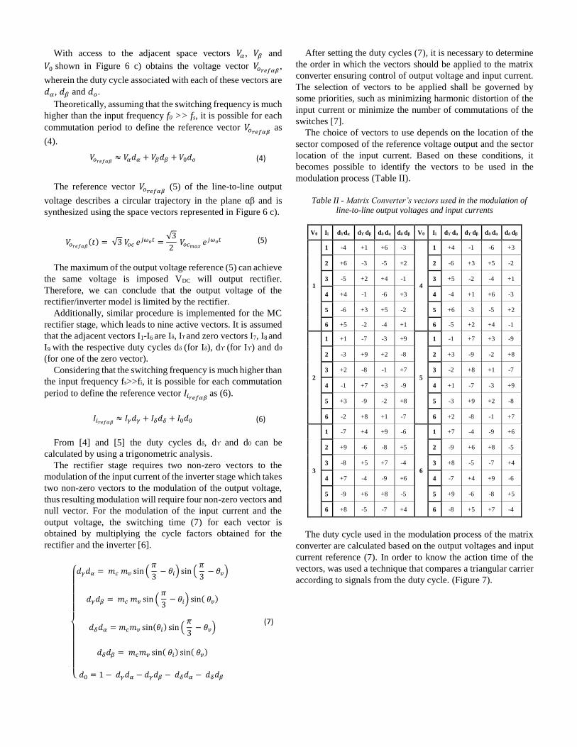
The choice of vectors to use depends on the location of the
sector composed of the reference voltage output and the sector
location of the input current. Based on these conditions, it
becomes possible to identify the vectors to be used in the
modulation process (Table II).
Table II - Matrix Converter’s vectors used in the modulation of
line-to-line output voltages and input currents
V0 Ii dϒdα dϒ dβ dδ dα dδ dβ V0 Ii dϒ dα dϒ dβ dδ dα dδ dβ
1
1 -4 +1 +6 -3
4
1 +4 -1 -6 +3
2 +6 -3 -5 +2 2 -6 +3 +5 -2
3 -5 +2 +4 -1 3 +5 -2 -4 +1
4 +4 -1 -6 +3 4 -4 +1 +6 -3
5 -6 +3 +5 -2 5 +6 -3 -5 +2
6 +5 -2 -4 +1 6 -5 +2 +4 -1
2
1 +1 -7 -3 +9
5
1 -1 +7 +3 -9
2 -3 +9 +2 -8 2 +3 -9 -2 +8
3 +2 -8 -1 +7 3 -2 +8 +1 -7
4 -1 +7 +3 -9 4 +1 -7 -3 +9
5 +3 -9 -2 +8 5 -3 +9 +2 -8
6 -2 +8 +1 -7 6 +2 -8 -1 +7
3
1 -7 +4 +9 -6
6
1 +7 -4 -9 +6
2 +9 -6 -8 +5 2 -9 +6 +8 -5
3 -8 +5 +7 -4 3 +8 -5 -7 +4
4 +7 -4 -9 +6 4 -7 +4 +9 -6
5 -9 +6 +8 -5 5 +9 -6 -8 +5
6 +8 -5 -7 +4 6 -8 +5 +7 -4
The duty cycle used in the modulation process of the matrix
converter are calculated based on the output voltages and input
current reference (7). In order to know the action time of the
vectors, was used a technique that compares a triangular carrier
according to signals from the duty cycle. (Figure 7).

dϒ dα
dϒ dβ
dδ dα
dδ dβ
d0 dϒ dα
dϒ dβ
dδ dα
dδ dβ
dϒ dα
dϒ dβ
dδ dα
dδ dβ
d0 dϒ dα
dϒ dβ
dδ dα
dδ dβ
Du
ty C
ycle
Sig
na
ls
Time
Figure 7 - Modulation process used to select the space vectors and
the time interval when they are applied
The selection of vectors to be applied in the control of matrix
converter is not only based on the analysis of Figure 7 but also
in Table II.
Figure 7 show the driving time of each vector. This
information together with the location of the input current and
the output voltage follows for Table II, from which the result
vectors to be applied to three-phase matrix converter switches.
The Figure 8 is a simplified way of obtaining the final vector
to apply to the matrix converter.
dϒ dα
dϒ dβ
dδ dα
dδ dβ
d0 dϒ dα
dϒ dβ
dδ dα
dδ dβ
dϒ dα
dϒ dβ
dδ dα
dδ dβ
d0 dϒ dα
dϒ dβ
dδ dα
dδ dβ
Du
ty C
ycle
Sig
na
ls
Tempo
S11
Va
Vb
Vc
Ia
Ib
Ic
S12
S13
S21 S31
S22 S32
S13 S13
IA IB IC
VA VB VC
Tdϒ dα Vector -4
Input current LocationOutput Voltage
Location
1 1
Figure 8 - Selection scheme for the SVM vectors
SST proposed in this paper, the modulation method must be
modified to ensure non-saturation of the high frequency
transformer.
E. Modified SVM
Modified SVM is a switching a strategy based on SVM that
to ensure non-saturation of transformer. Figure 9 represents the
modulation process already used with appropriate
modifications to prevent saturation of the transformer.
III. CONTROL OF THE OUTPUT CURRENT
The current regulator block diagram is show in Figure 8,
where 𝐼𝑜𝑑𝑞𝑟𝑒𝑓 is the reference current and 𝐼𝑜𝑑𝑞 the load current.
Both are multiplied by αi, the current sensor gain, and the
difference between the two currents, i.e., the current error is
applied to the controller Ci(s). This controller generates the
modulating voltage used by the SVM.
LoadHdq V0dq I0dq
αi
αi
I0dq ref
+ -
Figure 8 – Output current regulator block diagram
C(s) is a Proportional-Integral (PI) Controller, which
ensures a dynamic second order closed chain. This
compensator ensures a null static error and an acceptable rise
time.
For the sizing of the current regulator, the three-phase matrix
converter can be represented as transfer function of the first
order (8) with a given delay time Td.
𝐺(𝑠) =1
1 + 𝑠 𝑇𝑑 (8)
To calculate the Tz and Tp parameters, it is considered that
the zero of C (s) cancels the lowest frequency pole, introduced
by the output filter. From (9), one obtains Tz where Rout is the
sum of the internal resistance of the coil with the load
resistance.
𝑇𝑧 = 𝐿𝑜𝑢𝑡𝑅𝑜𝑢𝑡
(9)
The value of Tp is calculated by (10), where αi is the current
gain and Td is the average delay of the system.
𝑇𝑝 = 2 𝛼𝑖 𝑇𝑑𝑅𝑜𝑢𝑡
(10)
Three-Phase Matrix ConverterModular Matrix Converter
1 2 3 4
Signal Modified SVM
High Frequency Transformer
Gate
Gate
SVM+1
-1
Figure 9 – Modified SVM

IV. CONTROL OF THE OUTPUT VOLTAGE
In sizing the voltage controller, care has based on this single-
line diagram in Figure 9.
System
ISystem ILoad
ic
VLoadCf1
Figure 9- Load voltage regulator
The voltage regulator has to ensure that the load voltage,
which is the same as the capacitor voltage (11).
𝑉𝐿𝑜𝑎𝑑 = 𝑖𝑐𝑠𝐶𝑓1
(11)
In the design of the controller, it is considered that the load
current (Iload) is a disturbance of the system [8], [9]. As the
current output of the matrix converters is controlled, it is also
possible to consider that the matrix converters, filters and
transformer leakage inductances can be represented by the
current source Isystem.
In Figure 10 is presented the voltage regulator block diagram,
wherein the block
𝐺𝑖𝛼𝑖⁄
𝑠𝑇𝑑+1 represents the matrix converter
controlled by current, [10].
Iref matrix Iline VLoad
αv
αv
VLoad ref
+ -
ILoad
+
- Ic
Figure 10 – Block diagram of the voltage regulator
Finally, the proportional gain Kp and the integral gain Ki are
obtain by (12):
{
𝐾𝑝 =
2.15𝐶𝑓1𝛼𝑖
𝛼𝑣𝑇𝑑(1.75)2
𝐾𝑖 =𝐶𝑓1 𝛼𝑖
𝛼𝑣𝑇𝑑2(1.75)3
(12)
V. RESULTS
The SST developed in this dissertation was implemented in
MATLAB / Simulink software in order to evaluate and test the
performance and robustness in several operating scenarios.
A. Scenario 1 – Ideal conditions
In the first scenario is take analysis of the system before
normal operation without any disruption in the network.
In this dissertation was used High frequency transformer
with a power of 630KVA with a working frequency of 2000Hz
In Figure 11 and Figure 12 are shown the waveforms of the
voltage in the load as well as the respective current.
The waves have a sinusoidal forms with a fundamental
frequency of 50Hz.
Figure 11 – Line to-neutral load voltage
Figure 12 – Load current
In Figure 13 was compared the reference voltage with the
control voltage, and conclude that the reference tracking is
achieved with a greatly reduce error.
Figure 13- Line-to neutral load reference voltage (Red), and line-
to-neutral load voltage (Blue))
Figure 14 – Error between in reference voltage and control
voltage.
0.25 0.255 0.26 0.265 0.27 0.275 0.28 0.285 0.29-400
-300
-200
-100
0
100
200
300
400
Tens
ão [V
]
Tempo [s]
0.25 0.255 0.26 0.265 0.27 0.275 0.28 0.285 0.29-400
-300
-200
-100
0
100
200
300
400
Corre
nte
[A]
Tempo [s]
0.25 0.255 0.26 0.265 0.27 0.275 0.28 0.285 0.29-400
-300
-200
-100
0
100
200
300
400
Tens
ão [V
]
Tempo [s]
0.21 0.22 0.23 0.24 0.25 0.26 0.27 0.28 0.29-3
-2
-1
0
1
2
3
Tens
ão [V
]
Tempo [s]

Figure 15 represents the output voltage of the modular matrix
converter, applied to a primary winding.
Figure 16 represents the input voltage of the three-phase
converter.
Figure 15 – Voltage applied to a primary winding of transformer
Figure 16 - Voltage applied to a secondary winding of transformer
Figure 17 represents the input currents of SST. The currents
contais the high frequency harmonics arising from the high-
frequency semiconductor switching converters.
Figure 17 – Input currents of SST (MV)
B. Scenario 2 – Voltage sag
In this section it was the behavior of the SST when
confronted with a voltage sag on the medium voltage.
In Figure 18 can check the wave disturbance in the input
voltage. The perturbance caused a lowering in input voltage
during two periods of the network.
Figure 18 – Medium voltage.
Figure 19 represents the load voltage, and it can be concluded
that the voltage suffered no change.
Figure 19 – Load voltage
In Figure 20 was compared the reference voltage with the
control voltage, and conclude that the reference tracking is
achieved with a greatly reduce error.
Figure 20 - Line-to neutral load reference voltage (Red), and line-
to-neutral load voltage (Blue))
C. Scenario 2 – Voltage swell
In this section, the behavior of the SST was evaluated for a
voltage swell on the medium voltage.
In Figure 21 it can be seen the wave disturbance in the input
voltage. The disturbance caused a substantial increase in the
input voltage during two periods of the grid.
0.02 0.022 0.024 0.026 0.028 0.03 0.032 0.034 0.036 0.038 0.04-5000
-4000
-3000
-2000
-1000
0
1000
2000
3000
4000
5000
Tens
ão [V
]
T [s]
0.02 0.022 0.024 0.026 0.028 0.03 0.032 0.034 0.036 0.038 0.04-600
-400
-200
0
200
400
600
Tens
ão [V
]
T [s]
0.25 0.255 0.26 0.265 0.27 0.275 0.28 0.285 0.29-100
-80
-60
-40
-20
0
20
40
60
80
100
Corre
nte
[A]
Tempo [s]
0.16 0.18 0.2 0.22 0.24 0.26 0.28-1
-0.8
-0.6
-0.4
-0.2
0
0.2
0.4
0.6
0.8
1x 10
4
Tens
ão [V
]
Tempo [s]
0.16 0.18 0.2 0.22 0.24 0.26 0.28-400
-300
-200
-100
0
100
200
300
400
Tens
ão [V
]
Tempo [s]
0.16 0.18 0.2 0.22 0.24 0.26 0.28-400
-300
-200
-100
0
100
200
300
400
Tens
ão [V
]
Tempo [s]

Figure 21 – Medium voltage
Figure 22 the sinusoidal load voltage. Faced with an voltage
swell at the entrance of the SST, the waveforms of voltages
underwent no significant changes, which shows the good
response of the SST.
Figure 22 – Load voltage
In Figure 23 was compared the reference voltage with the
control voltage, and conclude that the reference tracking is
achieved with a greatly reduce error
Figure 23 - Line-to neutral load reference voltage (Red), and line-
to-neutral load voltage (Blue))
D. Scenario 3 – Harmonic Distortion on the medium
voltage
In this operating scenario, consider the existence of
harmonics of the medium voltage. In the test scenario is
considered the 5th harmonic, ensuring that its amplitude does
not exceed the threshold of 6% set by the standard (EN 50160).
In Figure 24 is represented the wave of the input voltage in
SST. There is the effect of the 5th harmonic, responsible for
wave distortion of the input voltage.
Figure 24 – Medium voltage
The voltage at the load (Figure 25) shows a nearly sinusoidal
wave with a small ripple.
Figure 25 – Load voltage
VI. CONCLUSIONS AND FUTURE WORK
This work aimed to develop a electronic power transformer
for distribution systems, capable of producing voltages of
variable magnitude and frequency at the output.
During the development of this project, emerged several
concerns, such as non-saturation of the transformer, that with
the change in the characteristics of the modulation SVM was
achieved. Another major concern is the limited voltage imposed
by semiconductor constituting the matrix converters, not
facilitating the integration of the matrix converter in the
medium-voltage side.
Known the problem, we developed a modular matrix
converter, which regulates the voltage to levels that do not cast
doubt on the operability of used converters.
The current controller, based in PI controller, was tested with
a good performance, with a static error close to zero, and
allowing a quick response while ensuring system stability for
various load scenarios. The power factor might not be unitary
since it depends on the input filter and the load conditions.
Finally, it is important to note that this system has many other
utilities that may be developed in the near future, such as
integration into a smart grid or in substations fitted to renewable
energy systems.
REFERENCES
[1] van der Merwe, J., W.; du T. Mouton, H.; “The solid-state transformer
concept: A new era in power distribution,” in AFRICON 2009, 2009;
[2] Hassan, R.; Radman, G.; "Survey on Smart Grid" IEEE 2010
SoutheastCon, Proceedings of the power electronic application
0.16 0.18 0.2 0.22 0.24 0.26 0.28
-1
-0.5
0
0.5
1
x 104
Tens
ão [V
]
Tempo [s]
0.16 0.18 0.2 0.22 0.24 0.26 0.28-400
-300
-200
-100
0
100
200
300
400
Tens
ão [V
]
Tempo [s]
0.16 0.18 0.2 0.22 0.24 0.26 0.28-400
-300
-200
-100
0
100
200
300
400
Tens
ão [V
]
Tempo [s]
0.25 0.255 0.26 0.265 0.27 0.275 0.28 0.285 0.29-1
-0.8
-0.6
-0.4
-0.2
0
0.2
0.4
0.6
0.8
1x 10
4
Tens
ão [V
]
Tempo [s]
0.25 0.255 0.26 0.265 0.27 0.275 0.28 0.285 0.29-400
-300
-200
-100
0
100
200
300
400
Tens
ão [V
]
Tempo [s]

conference, vol., no., pp.210–213, March 2010;
[3] She, X.; “Review of Solid-State Transformer Technologies and Their
Application in Power Distribution Systems”, Future Renewable Electr.
Energy Delivery & Manage. Syst. Center, North Carolina State Univ.,
2013;
[4] Huber, L., Borojevic, D., Burany, N., Analysis, Design and
Implementation of the Space-Vector Modulator for Forced- Commutated
Cycloconverters; IEE Proceedings-B Electric Power Applications, vol
139, No 2, March 1992;
[5] Nielsen, P.; Blaabjerg, F.; Pedersen, J.; “Space-Vector Modulated Matrix
Converter with Minimized number of Switchings and a Feedforward
Compensation of Input Voltage Unbalance”; Proc. PEDES’96
Conference, Vol. 2, pp. 833-839, New Delhi, India.
[6] Huber, L.; Borojevic, D.; “Space Vector Modulated Three-Phase to
Three-Phase Matrix Converter with Input Power Factor Correction”;
IEEE Transactions on Industry Applications, Vol. 31, No 6, pp. 1234 -
1246, November/December 1995.
[7] Nielsen, P.; Blaabjerg, F.; Pedersen, J.; “Space-Vector Modulated Matrix
Converter with Minimized number of Switchings and a Feedforward
Compensation of Input Voltage Unbalance”; Proc. PEDES’96
Conference, Vol. 2, pp. 833-839, New Delhi, India.
[8] Pinto, S., Silva, J. F., Silva, F., Frade, P., Design of a Virtual Lab to
Evaluate and Mitigate Power Quality Problems Introduced by
Microgeneration, in “Electrical Generation and Distribution Systems and
Power Quality Disturbances, Intech, 2011.
[9] Alcaria, P, Pinto, S. F., Silva, J. F., Active Voltage Regulators for Low
Voltage Distribution Grids: the Matrix Converter Solution, Proc. 4th
International Conference on Power Engineering, Energy and Electrical
Drives, PowerEng 2013, pp 989-994, Istanbul, Turkey, May 2013.
[10] Pinto, S.; Silva, J.; Gambôa, P.; “Current Control of a Venturini Based
Matrix Converter”, IEEE International Symposium on Industrial
Electronics – ISIE 2006, Vol. 4, pp. 3214 – 3219, Montréal, Canada, July
2006.


