
Electronic Fundamentals I Page 7-1
The Bipolar Junction Transistor
The BJT is a three terminal device whose output current, voltageand power are controlled by its input
In communication systems, the transistor is used as the primarycomponent in an , a circuit that is used to increase thestrength of an ac signal.
There are two basic types of transistors that we will be studying.
The Bipolar Junction Transistor (BJT)The Field Effect Transistor (FET)
The term “transistor” usually refers to the BJT. Field EffectTransistors are generally referred to as a FET.
The BJT is a three terminal device , the terminals called ,, and .
The collector and emitter are made up of the same type of semi-conductor material ( or type) while the base is made up of theother type.
There are two types of BJTspnp - --- ---
current.
amplifier
p type n type p type
p n
collector base emitternpn - --- ---n type p type n typecollector base emitter
�
�
�
�
The BJT (Bipolar Junction Transistor)
theemitter the base the collector
Transistors
Electronic Fundamentals IPage 7-2
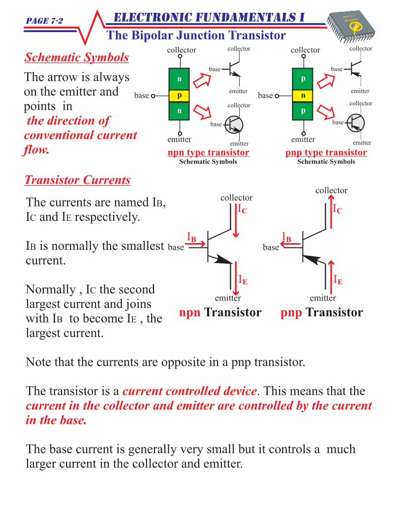
pnp type transistor
p
p
nbase
collector
emitter
base
collector
emitter
base
collector
emitter
Schematic Symbols
p
n
n
base
collector
emitter
npn type transistor
base
collector
emitter
base
collector
emitter
Schematic Symbols
Schematic Symbols
The arrow is alwayson the emitter andpoints inthe direction of
conventional currentflow.
Transistor Currents
base
collector
IC
IE
IB
emitter
pnp Transistor
base
collector
IC
IE
IB
emitter
npn Transistor
The currents are named I ,I and I respectively.
Normally , I the secondlargest current and joinswith I to become I , thelargest current.
Note that the currents are opposite in a pnp transistor.
The transistor is a . This means that the
The base current is generally very small but it controls a muchlarger current in the collector and emitter.
B
C E
C
B E
I is normally the smallestcurrent.B
current controlled devicecurrent in the collector and emitter are controlled by the currentin the base.
The Bipolar Junction Transistor

Electronic Fundamentals I Page 7-3
DC Current Gain ( )�
Transistor Construction & Operation
An increase or decrease in the value of I causes a larger but
similar change in I and I .B
C E
The value of I is generally some multiple of I . This factor by
which the current increases from base to collector is called the
forward dc current gain of the device ( beta) also called h
If I is 50 A and is 120 then :
C B
�
� �
FE.
B
Examplecollector
IE
IB= 50 A�
IC= 6 mA
emitter
npn Transistor
IC =
=
=
IB�
6 mA(50 A)�(120)
n
n
n
p
Emitter
Collector
Base
|
Base - emitterdepletion region
Collector - basedepletion region
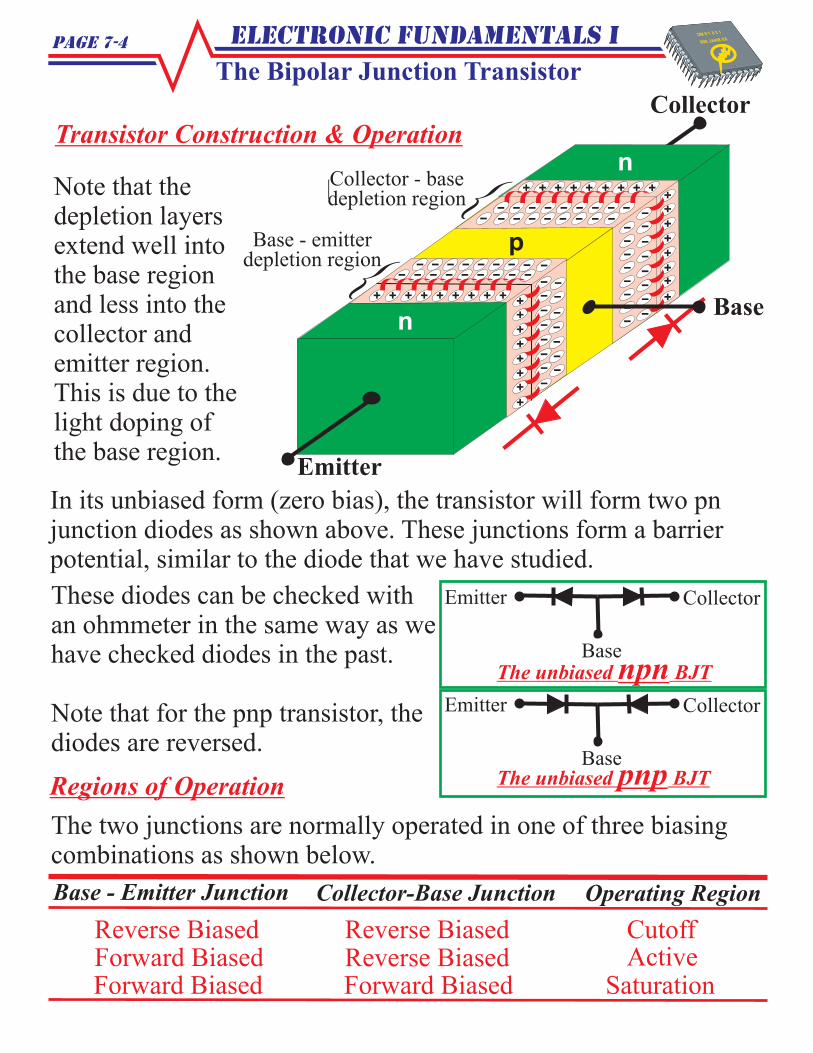
The transistor ismade of 3 typesof semi-conductormaterials thatform twojunctions asshown. Note thewire connectionto each of thebase, collectorand emitter.
pn
The Bipolar Junction Transistor
Electronic Fundamentals IThe Bipolar Junction Transistor
Page 7-4
Transistor Construction & Operation
n
n
n
p
Emitter
Collector
Base
|
Base - emitterdepletion region
Collector - basedepletion region
Note that thedepletion layersextend well intothe base regionand less into thecollector andemitter region.This is due to thelight doping ofthe base region.
In its unbiased form (zero bias), the transistor will form two pnjunction diodes as shown above. These junctions form a barrierpotential, similar to the diode that we have studied.
Base
Base
Collector
Collector
Emitter
Emitter
The unbiased BJTnpn
The unbiased BJTpnp
These diodes can be checked withan ohmmeter in the same way as wehave checked diodes in the past.
Note that for the pnp transistor, thediodes are reversed.
Regions of Operation
Base - Emitter Junction Collector-Base Junction Operating Region
Reverse BiasedForward BiasedForward Biased Forward Biased Saturation
Reverse BiasedReverse Biased
CutoffActive
The two junctions are normally operated in one of three biasingcombinations as shown below.

Electronic Fundamentals IThe Bipolar Junction Transistor
B
Page 7-5
The Cutoff Region
Base - Emitter Junction Collector-Base Junction Operating Region
Reverse Biased Reverse Biased Cutoff
+
-
+
+
+-
-
p
n
n
VCC
VCE
VBE
RC
RE
RB
VBB
Transister Biased to Cutoff
Here, both junctions are
Very little current flowsfrom the collector to theemitter.
The depletion zones arewide and extend well intothe base region.
When the transistor is incutoff, the collector toemitter terminals appear likean open switch.
The base to emitter junctionis reverse biased, and thiscauses the open switchaction between the collectorand emitter.
There is almost no currentflow in the collector toemitter circuit and V isapproximately equal to V
reverse biased.
CE
CC
+
-
+
+
+
-
-VCC
V
= VCE
CC
VBE
RC
RE
RB
I = 0C
C
E
B
VBB
Transister Biased to CutoffCollector to Emitter is like an open switch
~
C
E

Electronic Fundamentals IThe Bipolar Junction Transistor
Page 7-6
This is the opposite ofcutoff. is thecondition where
The maximum current inthe circuit is reached whenthe collector to emitterterminals appear like aclosed switch.
The maximum current (I )
in the circuit is nowdetermined by the formula
Now I = I no longer
holds true since increasingI does not increase I .
Further increasing I
forward biases bothjunctions of the transistor.
C
C B
B C
B
�
Saturationfurther
increases in I will not
cause increases in IB
C.
The Saturation Region
Base - Emitter Junction Collector-Base Junction Operating Region
Forward Biased Forward Biased Saturation
+
-
+
+
+
--
p
n
n
VCC
VCE
VBE
VCB
RC
RE
RB
VBB
Transistor Biased to Saturation
0.7 V
0.4 V
0.3 V
+
+
-
-
+
+
-
VCC
V
= 0.3 VCE
VBE
RC
RE
RB
IC
C
E
B
VBB
Transistor Biased to SaturationCollector to Emitter is like closed switch
~
I =CVCC
R + RC E
Electron
Flow

Electronic Fundamentals IThe Bipolar Junction Transistor
Page 7-7
The Active Region
Base - Emitter Junction Collector-Base Junction Operating Region
Forward Biased Reverse Biased Active
The transistor is said to be operating in the active region when thebase-emitter junction is forward biased and the collector-basejunction is reverse biased.
Generally, the transistor is operating in the active region when it isbetween cutoff and saturation.
To understand thetheory, consider
.
In Figure 1, SW
is open and nobase current isflowing.Therefore nocollector currentis flowing either.
r is heavily doped and contains many free electrons. Itsjob is to emit or inject electrons into the base. Until the base -emitter junction is forward biased by V , this cannot happen.
area is lightly doped and is very thin. It will pass most ofthe emitter ejected electrons on to the collector.
1
BB
electron flow.
The emitte
The base
+
-
+
+
-
p
n
n
VCC
VBE
RC
RB
VBB
SW1
I = 0B
I = 0C
Figure 1
Electron
Flow
Electron
Flow
Electron Flow

Electronic Fundamentals IThe Bipolar Junction Transistor
Page 7-8
The collector
Emitter Electrons
�
�
is so named because it or electronsfrom the base. Its doping level is between the heavy doping level ofthe emitter and the light doping level of the base.
At the moment before SW is closed, electrons from the emitter
have not entered the base region.
In Figure 2, SW is
closed and theemitter diode is nowforward biased.Electrons floodacross the junctionand into the baseregion.
Now they can flowin either of twodirections. They canflow to the left and out the base,or they can flow into the collector. Most will flow to the collector.
The reasons are:The base is lightly doped. Because of this electrons have along lifetime in the base. This gives then the time needed toreach the collector.The base area is very thin. This gives the electrons a betterchance of reaching the collector.
gathers collects
1
1
+
-
p
n
n
VCC
RC
VBB
SW1
I = 50 AB �
�= 120
I = 6 mAC
I = 50 A + 6 mAE �I = 6.05 mAE
The Biased TransistorFigure 2
Electron
Flow
Electron
Flow
Electron Flow
Electron Flow
Electron Flow
�

Electronic Fundamentals IThe Bipolar Junction Transistor
Electron
Flow
Page 7-9
To flow out of the base, electrons must recombine with holes in thebase. Then as valence electrons, they can flow out of the base andleave via the external wire.
Since the base is lightly doped and very thin, very few electronsmanage to re-combine and leave via the base lead.
Base Electrons
Collector Electrons
Almost all the free electrons go to the collector. Here they feel theattraction of V and leave via the collector lead. They flow
through R and return to the positive terminal of V
In most transistors,
CC
C CC
more than 95% of the emitter electrons flow tothe collector: less than 5% leave via the base
Electron Flow
Electron Flow
Summary (Using Conventional Current Flow)
Cutoff
+
-
+
+
-
VCC
V
= VCE
CC
I = 0C
I = 0BC
E
B
VBB
Collector to Emitter is like an open switch
~
B-E Junction Reverse B-E Junction Forward
C-B Junction Reverse
Collector Current (I )C
Approximately equal to zero
Collector Current (I )C
Maximum, limited only byexternal components in thecollector-emitter circuit.
C-B Junction Forward
Collector to Emitter is like a closed switch
Saturation
+
-
+
+
-
VCC
V
= 0.3 VCE
IC
IB
IE
C
E
B
VBB
~
B-E Junction Forward
Collector Current (I )C
Determined by the values of
and I (I = I )
�
�B C B
C-B Junction Reverse
Collector Current is beta times Base Current
Active
+
-
+
VCC
I = 6 mAC
I = 50 AB �
�= 120�
C
E
B
VBB I = 605 mAE .

Electronic Fundamentals IThe Bipolar Junction Transistor
Page 7-10
IB
IC
(B)
(C)
IE
(E)
Pnp TransistorCurrent Relationships
Transistor Currents
We know that a transistor is acurrent controlled device. Thismeans that
.
The magnitude of the change is
determined by the current gain ( ).
a small change in basecurrent produces a large changein both the emitter and collectorcurrents
�
Example 6.1 illustrates this point (p 208)
Relationships Between I , I , & IE C B
DC Beta ( )�
We already know the formula
and since I is usually much less than I : then the collector andemitter currents are approximately equal.
B C
I = IC E
I = I + IE B C
The rating of a transistor is the.
Remember that Beta is a ratio of current values and has
dc Beta ratio of dc collectorcurrent to dc base current
no units ofmeasure.
� =IC
IB
�
��
�
�� �
�I = IC B�

Electronic Fundamentals IThe Bipolar Junction Transistor
�
Page 7-11
This is an extremely important rating because most of the commontransistor circuits have and the
Other terminal currents can be found as:
Examples 6.2 , 6.3 , & 6.4 show how to use beta and any oneterminal current to find the other two terminal currents.
the input signal applied to the baseoutput signal taken from the collector
DC Alpha
The dc Alpha rating of a transistor is the ratio of collector currentto emitter current
Since I is always I + I , it will always be slightly larger than I .
This fact makes
is also referred to .
DC Alpha will usually be 0.9 or higher. Note that it is a ratio and
E C B C
� always slightly less than 1.
DC alpha collector current efficiency
� =IC
IE
Other useful formulas are:
You can determine the value of alpha from the value of beta withthis formula.
=�1 + �
�
IE = IC�I = IC E� IEIB = (1 - )�
I = I ( 1 + )E B �I = IC B�I = IC B�

Electronic Fundamentals IThe Bipolar Junction Transistor
Page 7-12
Maximum Current Ratings
Most transistor specification sheets list the maximum collectorcurrent rating for both saturation and cutoff. When a transistor issaturated , the collector current can go as high as several hundredmilliamperes. High power transistors can have current ratings ashigh as several amperes.
If we know the maximum collector current , we can find themaximum base current using this formula.
The beta rating is generally given as a range of values on the spec.sheet. We will be looking at this aspect later.
Example 6.6 demonstrates the use of this formula
IB(max) =IC(max)
�(max)
Maximum Cutoff Current Ratings
Transistor Voltages
Transistors also have a maximum cutoff current ratings. Theseratings are usually in the low nano-ampere range are specified forexact values of V and reverse VCE BE
We have seen that there a number of different voltagemeasurements involved when using transistors. the table belowlists them and the diagram shows their location.

Electronic Fundamentals IThe Bipolar Junction Transistor
Page 7-13
V This is a power supply voltage applied
directly or indirectly to the collector.
V The dc voltage used to bias the base of the
transistor. It may come directly from a dc voltage supply or it may beapplied indirectly to the base by a resistive circuit.
V . This is a supply voltage applied to the emitter.
In many cases V is simply a ground connection.
V The dc voltage measured from
V The dc voltage measured from
V The dc voltage measured from
V The dc voltage measured
V The dc voltage measured
V The voltage measured
refer to supply voltagesare voltages taken from a point to ground.
are voltages measured between twodifferent terminals.
CC
BB
EE
EE
C
B
E
CE
CB
BE
Collector Supply Voltage.
Base Supply Voltage.
Emitter Supply Voltage
collector to ground.
base to ground.
emitter to ground.
between the collector and the emitter.
between the collector and the base.
between the base and the emitter.
Double subscriptsSingle subscriptsTwo different subscripts
Remember
Transistor Voltages
C
E
B
VBB
VB
VE
VCE
VBE
VCB
VC
VCC
VEE
RC
RE

Electronic Fundamentals IThe Bipolar Junction Transistor
Page 7-14
Transistor Breakdown Ratings
Transistors have three breakdown ratings. These indicate themaximum reverse voltages that the transistor can withstand. If anyof these voltage maximums are exceeded, the transistor will likelybe destroyed.
6V
CollectorOpen
VEBO
BVEBOor
Transistor Voltage Ratings
V = 50 V - 0.75 V
= 49.25 VCB
C
E
B
VCB
V
50 VCE
V
0.75 VBE
There are several voltage ratings that we must concern ourselveswith when working with transistors.
Most spec sheets give a maximum value for this voltagefrom collector to base. It refers to the maximum amount of reversebias that can be applied to the collector- base junction withoutdamaging the transistor. This rating is important since this junctionis reverse biased for operation in the active region.For the circuit shown V is 50V and V is 0.75 V. V is thedifference between these or49.25 V If this voltage isgreater than the maximumrating for V that is specifiedin the spec sheet, then thetransistor will likely bedestroyed.
VCB
CE
BE CB
CB
This is the maximum allowablereverse voltage that the transistor can withstandfrom emitter to base. The “O” indicates that thecollector terminal is open when the rating ismeasured. This ensures that the BJT is in Cutoffwhen the parameter is measured.
VEBOBVEBO or

Electronic Fundamentals IThe Bipolar Junction Transistor
Page 7-15
BaseOpen
VCEO
BVCEOor
40V
EmitterOpen
VCBO
BVCBOor
60V
This is the maximum allowablereverse voltage that the transistor can withstandfrom collector to base. The “O” indicates that theemitter terminal is open. when the rating is
This is the maximumallowable reverse voltage that the transistorcan withstand from collector to emitter..The base terminal is open. when the rating ismeasured.
Transistor Characteristic Curves
There are three characteristic curves that describe the operation ofa transistor. These are the and curves.collector, base, beta
The Collector Curves
The characteristic collector curves relate to the values of I , I ,
and V .
Each collector curve is derived for a specific value of I .
C B
CE
B
Each collector curve is divided into 3 parts
�
�
VCBOBVCBO or
VCEOBVCEO or
Electronic Fundamentals IThe Bipolar Junction Transistor
Page 7-16
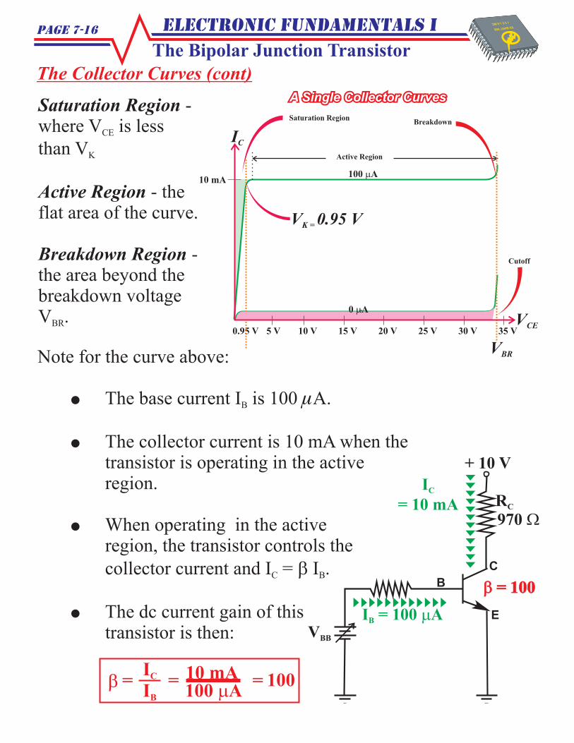
A Single Collector CurvesA Single Collector Curves
IC
V 0.95 VK =
VBR
VCE
100 A�
0
10 mA
5 V0.95 V 10 V 15 V 20 V 25 V 30 V 35 V
Saturation RegionBreakdown
Cutoff
Active Region
0 A�
Saturation Region
Active Region
Breakdown Region
-where V is less
than V
- theflat area of the curve.
-the area beyond thebreakdown voltageV .
CE
K
BR
Note for the curve above:
The base current I is 100 A.
The collector current is 10 mA when thetransistor is operating in the activeregion.
When operating in the activeregion, the transistor controls the
collector current and I = I .
The dc current gain of thistransistor is then:
�
�
�
�
B
C B
�
�
� = = =IC
IB 100 A�10 mA 100
970 �
+ 10 V
� = 100� = 100
C
E
B
RC
VBB
I = 100 AB �
I
= 10 mAC
The Collector Curves (cont)
� = 100

Electronic Fundamentals IThe Bipolar Junction Transistor
A Single Collector Curves
�
� = 100
Page 7-17
970 �
+ 10 V
� = 100� = 100
C
E
B
RC
VBB
I = 100 AB �
I
= 10 mACFor the same transistor circuit as shown
on the previous page, if I is 10 mA,
then what is the voltage across thecollector -emitter terminals.
This means that when I is 10 mA, the
transistor is in saturation.
We know from before that this transistorwill have a V of approximately 0.3 V
when it is saturated and in the fully “on”condition.
The figure opposite shows the terminalvoltages around the transistor atsaturation.
C
C
CE
VCC====
I RC CVCE
0.65V
0.3V
+ 10 V
VBB 0.95V
V is less than V and this
puts the transistor in thesaturation region.
V is around 0.95 V and
V is approx. 0.3 V. Note
the polarities of these andwe can see that V is the
difference between them.(Kirchoff’s Voltage Law)
CE K
BE
CE
CB
IC
V 0.95 VK =
VBR
VCE
100 A�
0
10 mA
5 V0.95 V 10 V 15 V 20 V 25 V 30 V 35 V
Saturation RegionBreakdown
Cutoff
Active Region
0 A�

Electronic Fundamentals IThe Bipolar Junction Transistor
Page 7-18
This difference voltage of 0.65 V is enough to forward bias theC-B junction. This means both junctions are forward biased andthe transistor is in saturation.
The Active Region
In the active region (where the curve is flat) the transistor acts likea constant current source. In this area, the transistor controls thecollector current (I ).
We know that the transistor is at saturation when R is at 970 . If
we reduce the value of R to 400 , then :
I has not changed but V has gone from 0.3 V to 6V in order to
maintain an I of 10 mA. The transistor is now well within the
active region. Remember that in this region the transistor willadjust to maintain I at constant current.
As you can see, changing the value of R does little to effect the
value of I . This is because the transistor’s dc current gain
controls the current here in the active region. The transistor adjusts
to keep the current at a value determines by I = I .
C
C
C
C CE
C
C
C
C
C B
�
�
�
VCC== 10V-10mA*400�= 10V - 4V= 6V
I RC CVCE
I = IC B�
(100)(100 A)�
10 mA
=
=and

Electronic Fundamentals IThe Bipolar Junction Transistor
Page 7-19
IC
V 6 VCE=
VBR
VCE
100 A�
0
10 mA
5 V0.95 V 10 V 15 V 20 V 25 V 30 V 35 V
Saturation RegionBreakdown
Cutoff
Active Region
0 A�
With R = 400 , the transistor isnow operating in the active region
C �
Operating Point
IC
V 6 VCE=
VBR
VCE
100 A�
150 A�
0
10 mA
15 mA
5 V0.95 V 10 V 15 V 20 V 25 V 30 V 35 V
0 A�
I increases from 100 A to 150 AI increases from 10 mA to 15 mA
The gain is still 100
B
C
�����������������
When the transistor isoperating in the activeregion --
I remains almost
constant for changes inV from V to V .
C
CE K BR
To change I , the
value of I or beta
must change.
C
B
What happens if we increase I ?B
We have raised I to 150 A.
Beta has not changednor has any of the circuitvalues.
I has increased to 15 mA.
By formula:
B
C
�
�I = 100 (150 A)
= 15 mA
I is dependant only on
beta and I .
C
C
B

Electronic Fundamentals IThe Bipolar Junction Transistor
�
Family of Collector CurvesFamily of Collector CurvesIC
VCE
100 A�
200 A�
300 A�
150 A�
250 A�
50 A�
0
30 mA
10 mA
20 mA
5 V 10 V 15 V 20 V 25 V 30 V 35 V
Saturation Region Breakdown
Cutoff
Active Region
0 A�
The Breakdown Region
The breakdown region is the area beyond V . If V increases into
this area, then I increases dramatically and the transistor will be
destroyed by the excessive heat.
BR CE
C
The Family of Characteristic Curves
When several I versus I curves are plotted, a composite graph is
created.This is the same example that we have been using.
Note that = 100 for each of the curves.
B C
�
Examples
I = IC B�
=
=
For the 150 A curve�
I = IC B�
=
=
For the 200 A curve�
I = IC B�
=
=
For the 300 A curve�
Page 7-20

Electronic Fundamentals IThe Bipolar Junction Transistor
IB
VBEVK
A Base Characteristic Curve
�
IC
The Relationship among Beta, I& Temperature
C
T=25 CO
T=100 CO
The Base Curves
The Beta Curves
The Base curve is a plot of I
versus V .
Note that it resembles theforward operating curve of thetypical diode.
B
BE
pn - junction
The beta curves show the relationship between beta andtemperature and/or collector current.
beta increases with temperaturebeta increases (up to a point) for increases in I
When I increases beyond a certain value, beta starts to
decrease.
C
C
�
�
�
Minimum Beta Condition
I = 0.1 mAC DC
I = 1.0 mAC DC
I = 10 mAC DC
I = 50 mAC DC
I = 100 mAC DC
4070
1006030
The spec. sheet for the 2N3904lists the following minimumbeta values.
Note that as I increases above
10 mA, the value of betadeceases.
C
Page 7-21
Family of Collector Curves

Electronic Fundamentals IThe Bipolar Junction Transistor
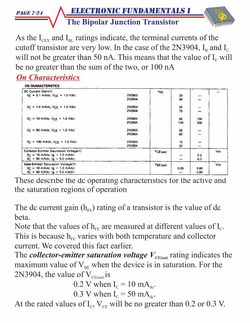
Transistor Specification Sheets
The transistor spec sheet gives us a wide variety of dc and acoperating characteristics. We will look at some of them.
Refer to the spec sheet on page 219 on the 2N3904
Maximum Ratings
The V , V , and V ratings are the maximum reverse ratings
that we studied earlier.
The device dissipation (P ) rating shows the 2N3904 has a P
rating of 625 mW when the ambient (room) temperature is 25 C.
If the case temperature (T ) is held at 25 C, the device P rating
increases to 1.5 Watts.
The case temperature can be held at 25 C with use of a fan or aheat sink.
CEO CBO EBO
D D
C D
O
O
O
Both ratings must be derated as temperature increases.
Page 7-22

Electronic Fundamentals IThe Bipolar Junction Transistor
Thermal Characteristics
The thermal ratings of the transistor are primarily used indevelopment applications.
Off Characteristics
These describe the operation of the transistor when it is operated incutoff.
The first 3 ratings are familiar. These are the maximum reversevoltage ratings that we have seen earlier. They are repeated herefor convenience.
The (I ) rating, indicates thecollector current maximum
value of I when the device is in cutoff.CEXcutoff
cutoff current maximum value
of base current present when the emitter-base junction is incutoff.
C
The base (I ) rating, indicates theBL
Page 7-23
Electronic Fundamentals IThe Bipolar Junction Transistor
On Characteristics
These describe the dc operating characteristics for the active andthe saturation regions of operation
The dc current gain (h ) rating of a transistor is the value of dc
beta.Note that the values of h are measured at different values of I .
This is because h varies with both temperature and collector
current. We covered this fact earlier.The rating indicates the
maximum value of V when the device is in saturation. For the
2N3904, the value of
FE
FE C
FE
BE
collector-emitter saturation voltage VCE(sat)
V is
0.2 V when I = 10 mA .
0.3 V when I = 50 mA .
At the rated values of I , V will be no greater than 0.2 or 0.3 V.
CE(sat)
C dc
C dc
C CE
As the I and I ratings indicate, the terminal currents of the
cutoff transistor are very low. In the case of the 2N3904, I and I
will not be greater than 50 nA. This means that the value of I will
be no greater than the sum of the two, or 100 nA
CEX BL
B C
E
Page 7-24

Electronic Fundamentals IThe Bipolar Junction Transistor
The rating the maximum
value of V when the device is in saturation. For the 2N3904, this
can be 0.85 V or 0.95 V depending on the rated value of I .
base-emitter saturation voltage VBE(sat)
BE
B
Transistor Testing
Transistors, like diodes, can be checked with an ohmmeter. Thisinvolves checking the forward and reverse resistance of the base-emitter diode and the collector-base diode. It is done in exactly thesame way we have done in the past with regular diodes.
Other checks are required to determine if the transistor will operatecorrectly, however this is a fast, first-line check to determine thecondition of the transistor. The transistor is bad if any of the diodechecks fail.
Checking the base-emitter diodeReverse Bias
Checking the base-emitter diodeForward Bias
Checking the collector-base diodeReverse Bias
Checking the collector-base diodeForward Bias
Page 7-25
C
B
E
C
B
E
C
B
E
C
B
E
Infinite ~700�
Infinite ~700�
Electronic Fundamentals I
Transistor Testing
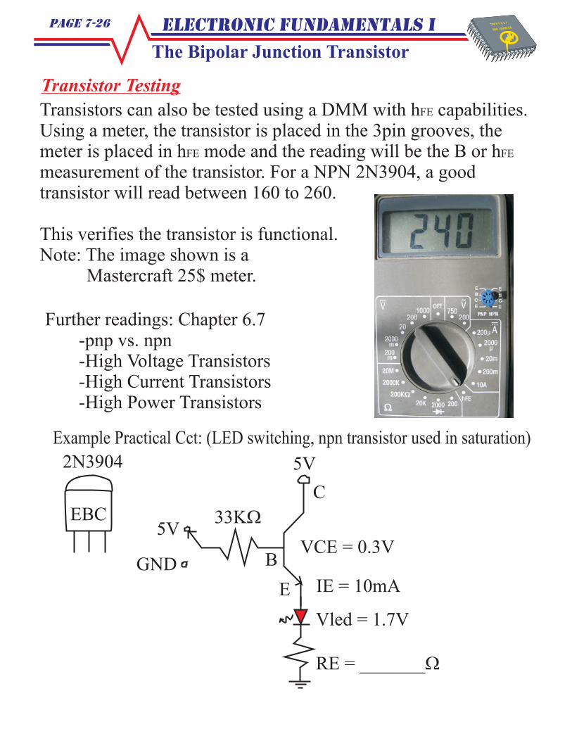
Transistors can also be tested using a DMM with h capabilities.Using a meter, the transistor is placed in the 3pin grooves, themeter is placed in h mode and the reading will be the B or hmeasurement of the transistor. For a NPN 2N3904, a goodtransistor will read between 160 to 260.
This verifies the transistor is functional.Note: The image shown is a
Mastercraft 25$ meter.
FE
FE FE
Page 7-26
Further readings: Chapter 6.7-pnp vs. npn-High Voltage Transistors-High Current Transistors-High Power Transistors
Example Practical Cct: (LED switching, npn transistor used in saturation)
EBC5V
GND
5V
33K�
IE = 10mA
Vled = 1.7V
VCE = 0.3V
2N3904
RE = _______�
C
B
E
The Bipolar Junction Transistor


