
Midterm Exam
Solutions

List at least 3 advantages of implementing selected portions of a complex design
in software
Problem 1
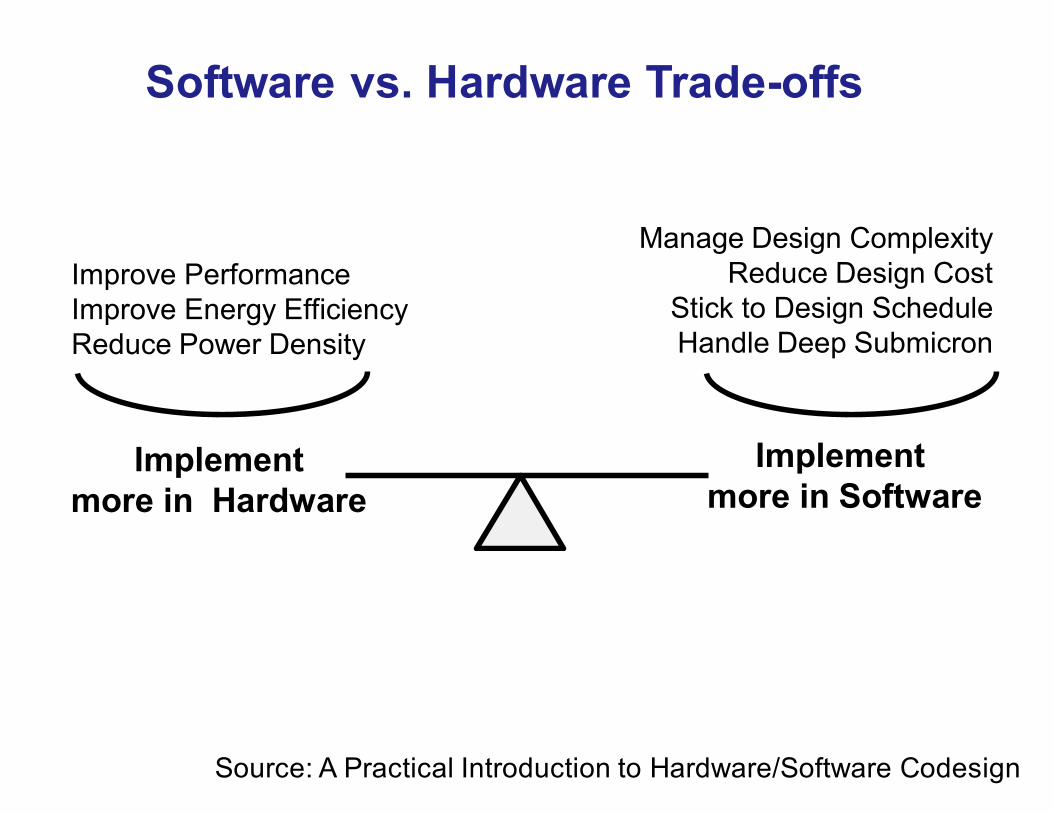
Software vs. Hardware Trade-offs
Implement more in Software
Implementmore in Hardware
Manage Design ComplexityReduce Design Cost
Stick to Design ScheduleHandle Deep Submicron
Improve PerformanceImprove Energy EfficiencyReduce Power Density
Source: A Practical Introduction to Hardware/Software Codesign

What are the primary advantages of Zynq All Programmable SoC over a traditional FPGA,
such as Virtex 7, with a soft microprocessor core, such as MicroBlaze?
Problem 2

• Clock frequency• Area• Power

Explain the term differentiation, and describe how Zynq can be
used to accomplish a high-level of differentiation
Problem 3

In economics and marketing, product differentiation (or simply differentiation)
is the process of distinguishing a product or service from others, to make it more attractive to
a particular target market. This involves differentiating it from competitors' products
as well as a firm's own products.

Choice Among Various Implementation Platforms
Source: Xcell Journal, no. 88, Q3 2014
List at least 4 major advantages of Vivado over ISE
Problem 4

Vivado Design Suite
• scalable data model, supporting designs with up to 100 million ASIC gate equivalents (GEs)
• based on industry standards, such as• AMBA AXI4 interconnect• IP-XACT IP packaging metadata• Tool Command Language (Tcl)• Synopsys Design Constraints (SDC)
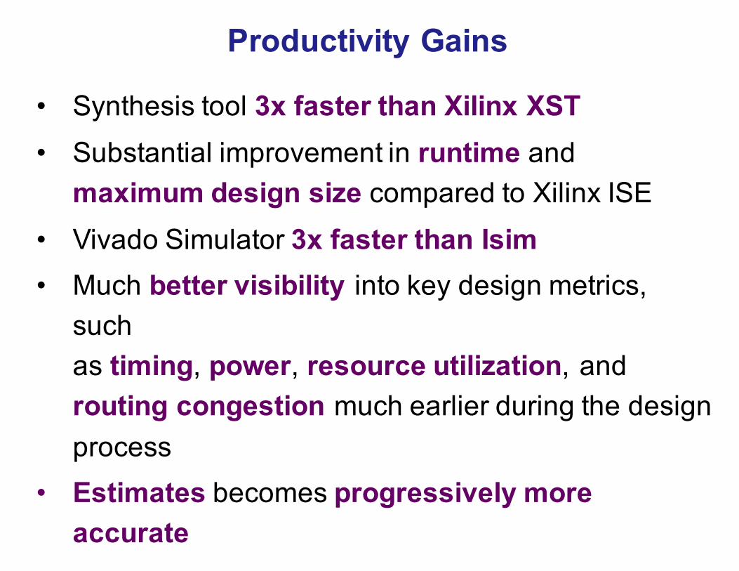
Productivity Gains
• Synthesis tool 3x faster than Xilinx XST• Substantial improvement in runtime and
maximum design size compared to Xilinx ISE• Vivado Simulator 3x faster than Isim• Much better visibility into key design metrics,
such as timing, power, resource utilization, and routing congestion much earlier during the design process
• Estimates becomes progressively more accurate

Multidimensional Analytical PlacerISE:• One-dimensional, timing-driven place-and-route algorithms• Simulated annealing algorithms that determine
randomly where the tool should place logic cells• Does adequate job for FPGAs below 1 million GEs
Vivado:• Modern multidimensional analytic placement algorithm• Deterministically finds a solution that primarily minimizes:
timing, congestion, and wire length• Better results, fewer iterations• Efficient up to 100 million GEs

Hierachical Chip Planning& Advantages of Standards
• ability to partition the design for processing by synthesis, implementation and verification
• divide-and-conquer team approach to big projects• design preservation feature enabling repeatable timing results• access to state of the art third-party EDA tools for tasks such as
• constraint generation• formal verification• static timing analysis
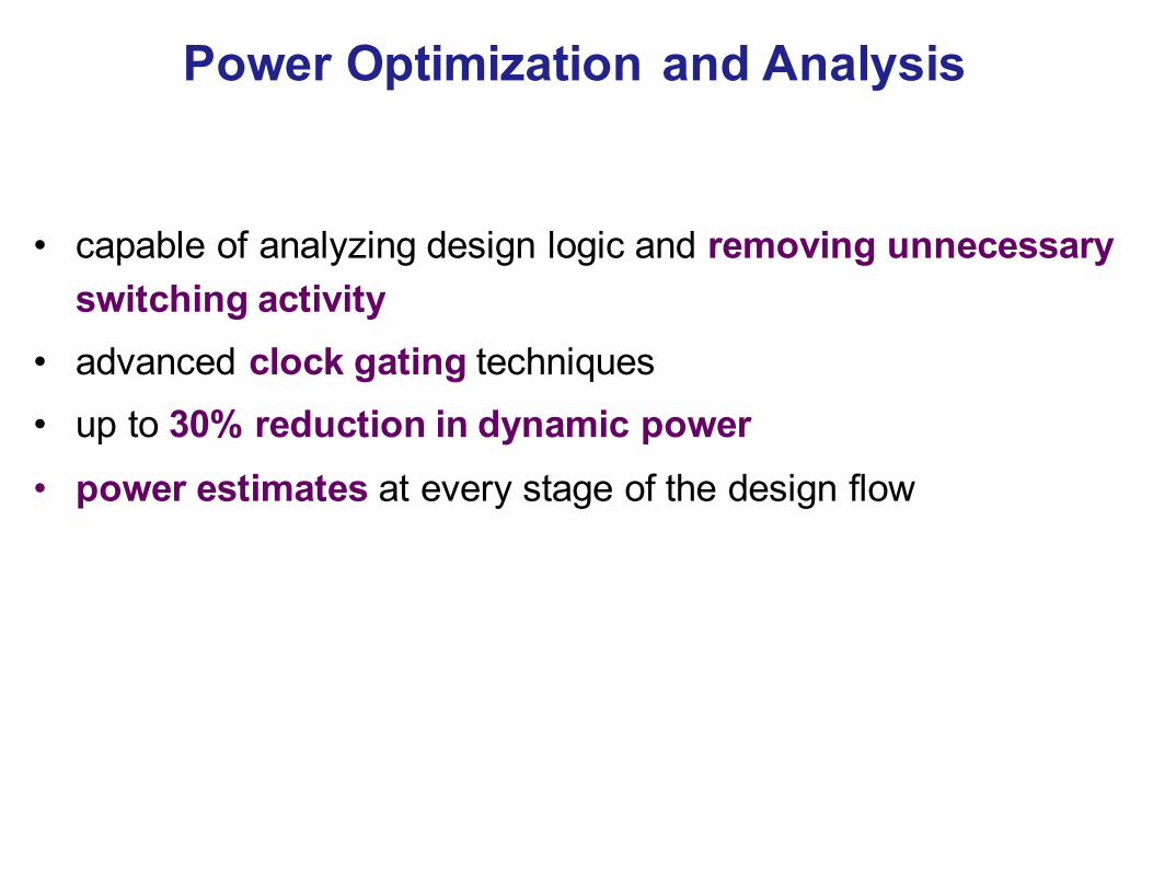
Power Optimization and Analysis
• capable of analyzing design logic and removing unnecessary switching activity
• advanced clock gating techniques• up to 30% reduction in dynamic power• power estimates at every stage of the design flow

IP Packager, Integrator, and Extensible IP Catalog
• any part of the design (including the entire design) can beturned into a reusable core at any level of the design flow:
• RTL• netlist• placed netlist• placed-and-routed netlist
• IP-XACT descriptions easy to integrate into future designs• IP Packager specifies the IP data using XML file• Extensible IP Catalog allows users to build their own standard
repositories from IP they’ve created, licensed from Xilinx, or licensed from third-party vendors
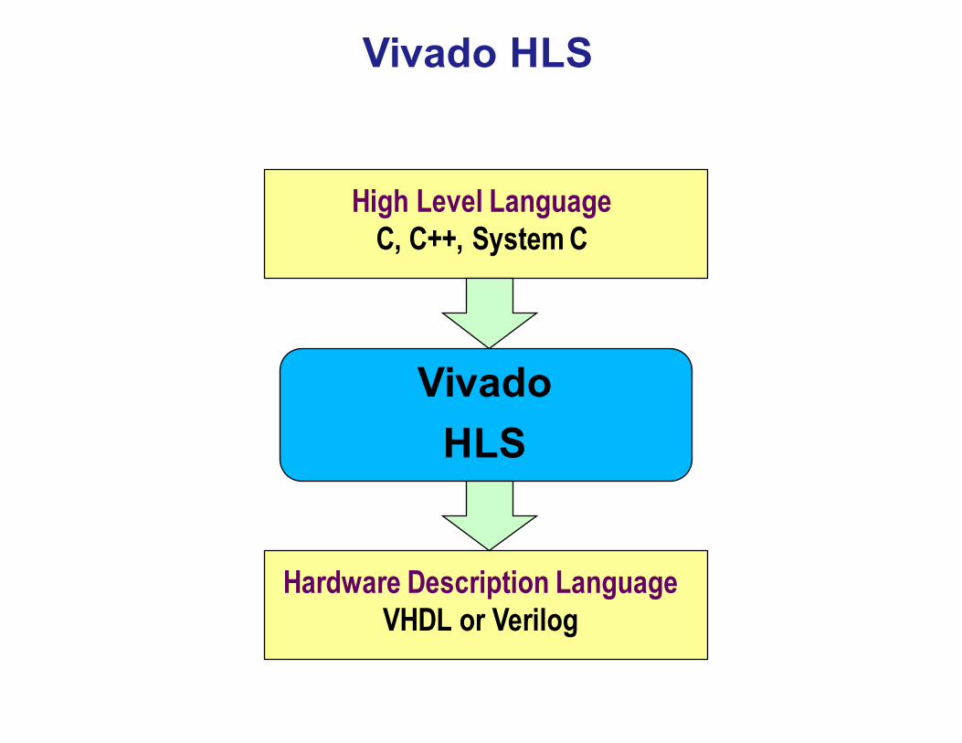
High Level LanguageC, C++, System C
Hardware Description LanguageVHDL or Verilog
VivadoHLS
Vivado HLS

List 4 families of Xilinx devices supported by both Vivado and ISE
Problem 5

Support for Xilinx Families
90 nm Spartan-3, Virtex-4
65 nm Virtex-5
45 nm Spartan-6
40 nm Virtex-6
28 nm Artix-7, Kintex-7, Virtex-7, Zynq 7000
Future families
ISE
Vivado

List 4 families of Xilinx devices supported by both Vivado and ISE
Problem 6

How many different types of interrupts can be generated by the AXI GPIO core?
Problem 5
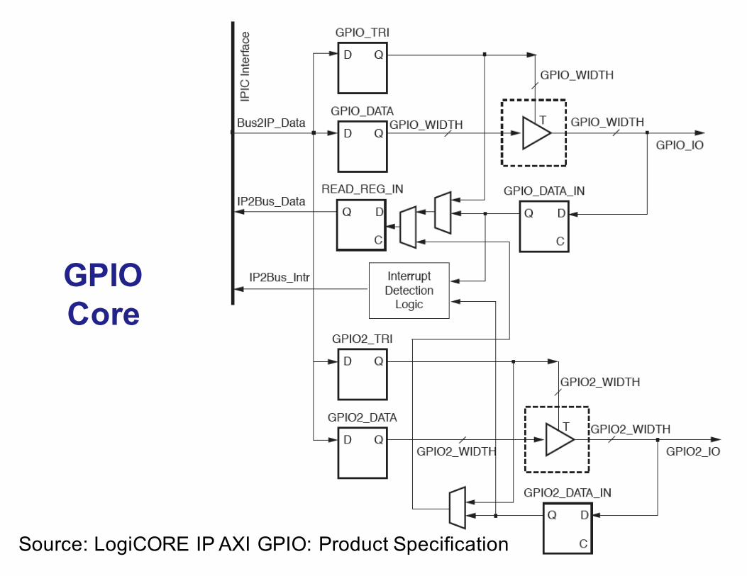
GPIO Core
Source: LogiCORE IP AXI GPIO: Product Specification

Source: LogiCORE IP AXI GPIO: Product Specification
Interrupt Status Registers, IP ISR
StatusStatus

Explain the ways of minimizing the area of the GPIO core, shown conceptually in the diagram below
Problem 7

Source: LogiCORE IP AXI GPIO: Product Specification
AXI GPIO Resource Utilization andMaximum Clock Frequency

Explain the role and functionality of GPIO_TRI registers, shown in the diagram above
Problem 8

What are the primary limitations of the Accelerator Coherency Port (ACP) of Zynq, which go against the idea of full coherency?
Problem 9
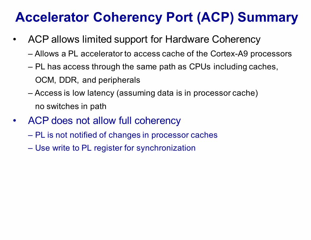
• ACP allows limited support for Hardware Coherency– Allows a PL accelerator to access cache of the Cortex-A9 processors– PL has access through the same path as CPUs including caches,
OCM, DDR, and peripherals– Access is low latency (assuming data is in processor cache)
no switches in path
• ACP does not allow full coherency– PL is not notified of changes in processor caches– Use write to PL register for synchronization
Accelerator Coherency Port (ACP) Summary

Explain the operation of the PWM mode of the AXI Timer (shown in the diagram below)
Problem 10
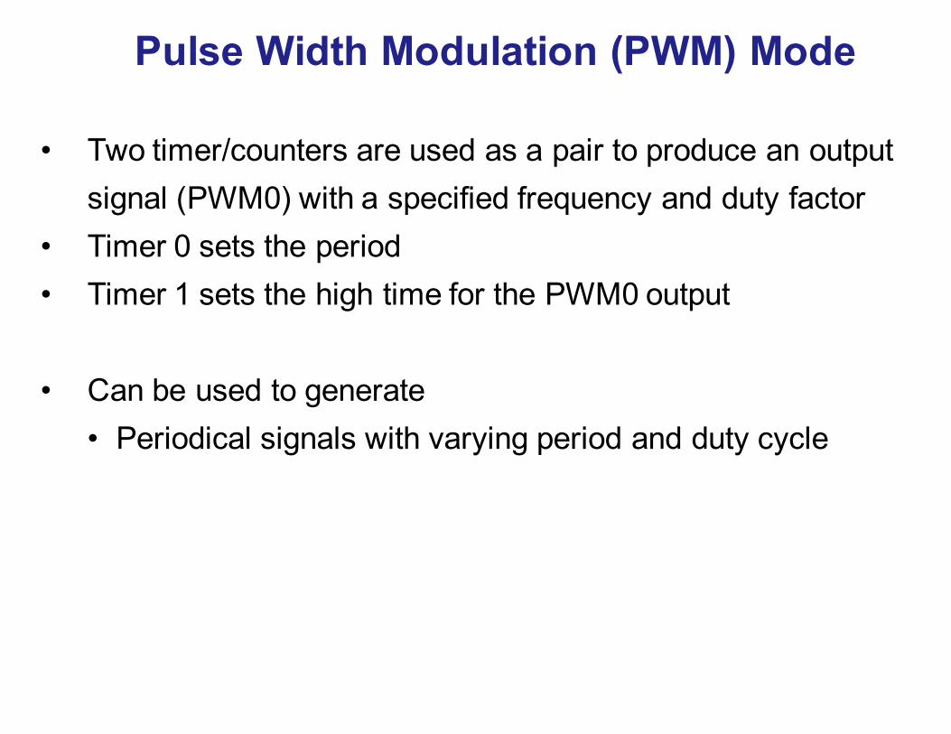
Pulse Width Modulation (PWM) Mode
• Two timer/counters are used as a pair to produce an output signal (PWM0) with a specified frequency and duty factor
• Timer 0 sets the period• Timer 1 sets the high time for the PWM0 output
• Can be used to generate• Periodical signals with varying period and duty cycle
Which mode of AXI Timer can be used to measure interval between two external events,such as two consecutive pushes of a button
connected to the pins of PL?
Problem 11
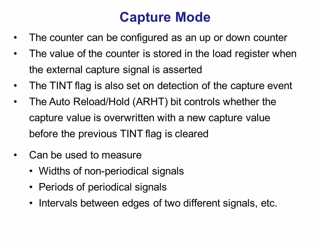
Capture Mode• The counter can be configured as an up or down counter• The value of the counter is stored in the load register when
the external capture signal is asserted• The TINT flag is also set on detection of the capture event• The Auto Reload/Hold (ARHT) bit controls whether the
capture value is overwritten with a new capture value before the previous TINT flag is cleared
• Can be used to measure• Widths of non-periodical signals• Periods of periodical signals• Intervals between edges of two different signals, etc.
Explain the difference between AXI Interconnect and AXI Interface
Problem 12

Interconnect vs. Interface
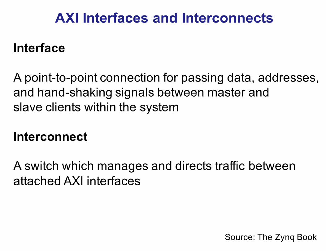
AXI Interfaces and Interconnects
Source: The Zynq Book
Interface
A point-to-point connection for passing data, addresses, and hand-shaking signals between master and slave clients within the system
Interconnect
A switch which manages and directs traffic between attached AXI interfaces

Explain the primary differences between AXI Full and AXI Stream Interfaces
Problem 13

Source: M.S. Sadri, Zynq Training
AXI Memory-Mapped vs. AXI Stream
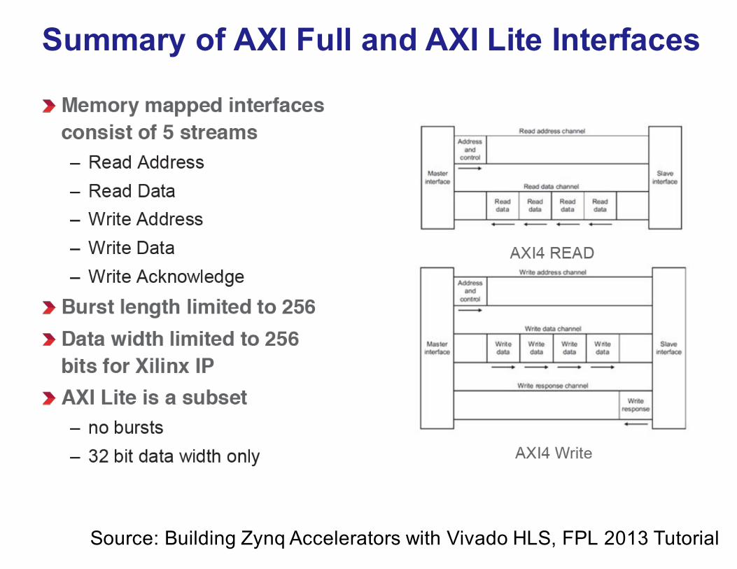
Summary of AXI Full and AXI Lite Interfaces
Source: Building Zynq Accelerators with Vivado HLS, FPL 2013 Tutorial

Summary of AXI Stream Interface
Source: Building Zynq Accelerators with Vivado HLS, FPL 2013 Tutorial

Provide the names of at least two System-on-Chip Bus Standards
competing with AMBA AXI4 standards
Problem 14

Bus Developedby
High-PerformanceShared Bus
PeripheralShared
Bus
Point-to-PointBus
AMBA v3 ARM AHB APBAMBA v4 ARM AXI4 AXI4-Lite AXI4-Stream
Coreconnect IBM PLB OPBWishbone SiliCore
Corp.Crossbar Topology
SharedTopology
Point to PointTopology
Avalon Altera Avalon-MM Avalon-MM Avalon-STAMBA: Advanced Microcontroller Bus ArchitectureAXI: Advanced eXtensible InterfaceAHB: AMBA High-speed BusAPB: AMBA Peripheral BusPLB: Processor Local BusOPB: On-chip Peripheral BusMM: Memory MappedST: Streaming
Competing System-on-Chip Bus Standards
Source: A Practical Introduction toHardware/Software Codesign

Explain the need for the highlighted operations in case of the DMA-based communication
between an ARM core and a hardware accelerator using GP Ports between PS and PL.
Problem 15
A. Write to Acceleratorprocessor allocates bufferprocessor writes data into bufferprocessor flushes cache for bufferprocessor initiates DMA transfer
B. Read from Acceleratorprocessor allocates bufferprocessor initiates DMA transferprocessor waits for DMA to completeprocessor invalidates cache for bufferprocessor reads data from buffer
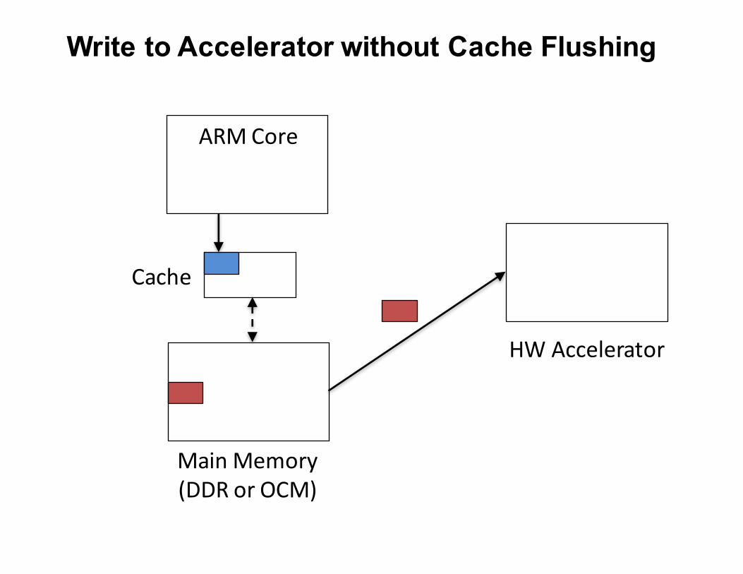
ARMCore
Cache
MainMemory(DDRorOCM)
HWAccelerator
Write to Accelerator without Cache Flushing
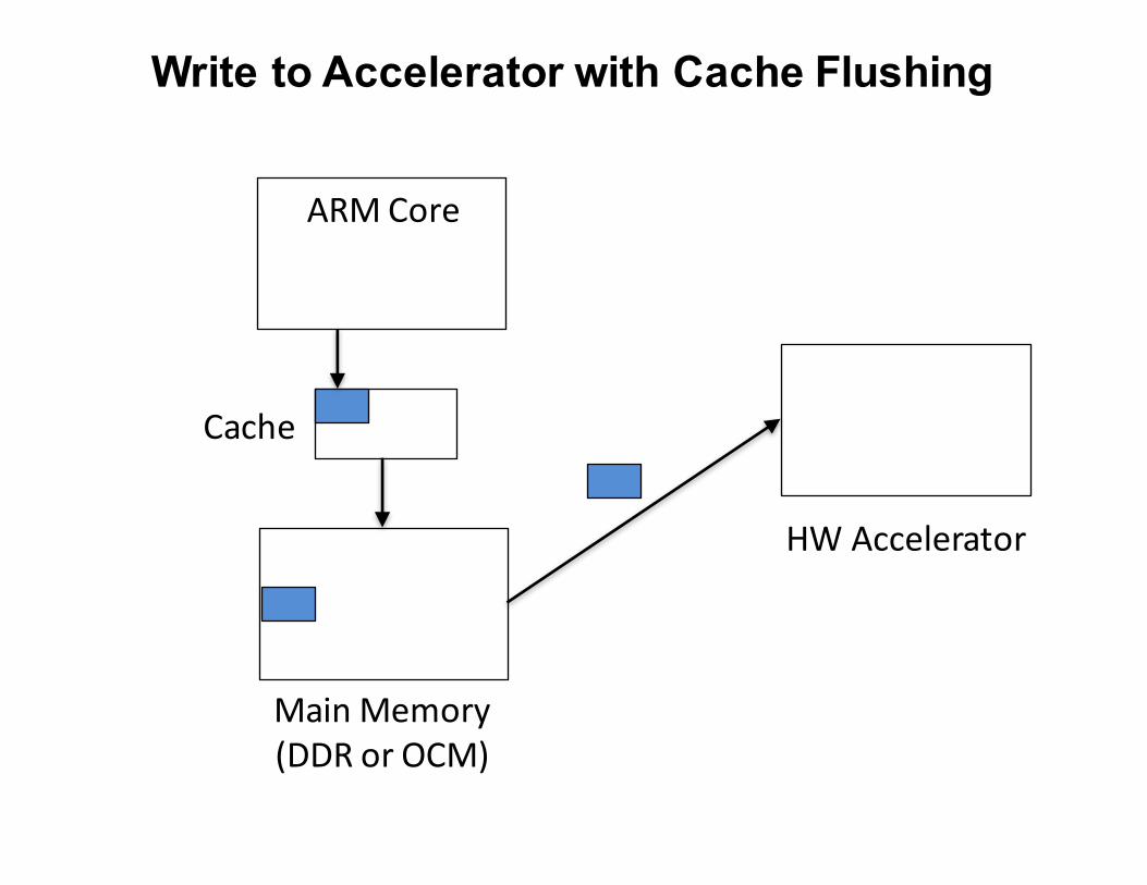
ARMCore
Cache
MainMemory(DDRorOCM)
HWAccelerator
Write to Accelerator with Cache Flushing

ARMCore
Cache
MainMemory(DDRorOCM)
HWAccelerator
Read from Accelerator without Invalidating Cache

ARMCore
Cache
MainMemory(DDRorOCM)
HWAccelerator
Read from Accelerator with Invalidating Cache

Explain the meaning of each number in the following estimate of
the maximum bandwidth supported by
Problem 16
A. HP ports of Zynq:
Maximum bandwidth = 4 * 64 bits * 150 MHz * 2 = 9.6 GByte/sec
B. external DDR
Maximum bandwidth = 1 * 32 bits * 2 * 533 MHz * 2 = 4.3 GByte/s
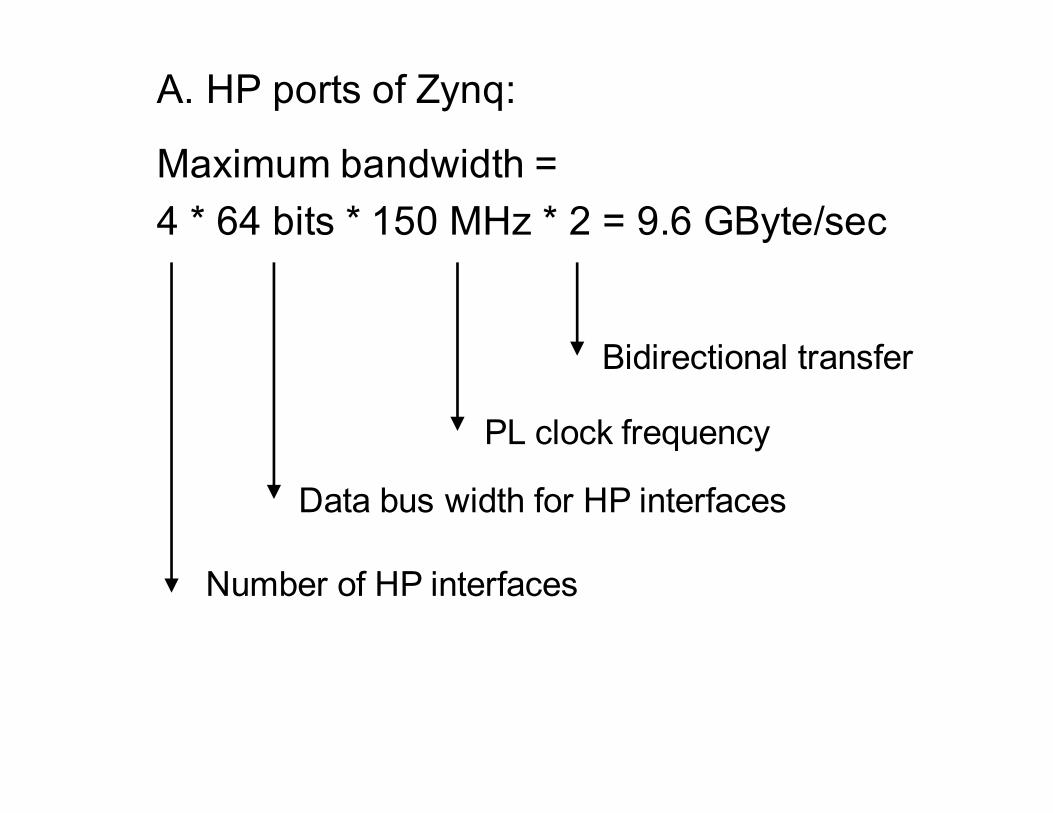
A. HP ports of Zynq:
Maximum bandwidth = 4 * 64 bits * 150 MHz * 2 = 9.6 GByte/sec
Bidirectional transfer
PL clock frequency
Data bus width for HP interfaces
Number of HP interfaces

B. external DDR
Maximum bandwidth = 1 * 32 bits * 2 * 533 MHz * 2 = 4.3 GByte/s
Bidirectional transfer
Maximum clock rate (clock frequency) of DDR3
Data bus width for DRAM interface
Number of DRAM interfaces
Double data rate (using both clk edges)

What operation starts a Scatter Gather DMA Transfer when using AXI DMA?
Problem 17
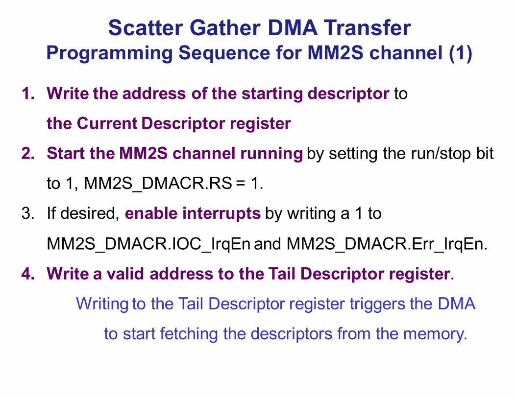
1. Write the address of the starting descriptor to
the Current Descriptor register2. Start the MM2S channel running by setting the run/stop bit
to 1, MM2S_DMACR.RS = 1.
3. If desired, enable interrupts by writing a 1 to
MM2S_DMACR.IOC_IrqEn and MM2S_DMACR.Err_IrqEn.
4. Write a valid address to the Tail Descriptor register.Writing to the Tail Descriptor register triggers the DMA
to start fetching the descriptors from the memory.
Scatter Gather DMA TransferProgramming Sequence for MM2S channel (1)

1. Write the address of the starting descriptor to
the Current Descriptor register2. Start the S2MM channel running by setting the run/stop bit
to 1, S2MM_DMACR.RS = 1.
3. If desired, enable interrupts by by writing a 1 to
S2MM_DMACR.IOC_IrqEn and S2MM_DMACR.Err_IrqEn.
4. Write a valid address to the Tail Descriptor register.Writing to the Tail Descriptor register triggers the DMA
to start fetching the descriptors from the memory.
Simple DMA TransferProgramming Sequence for S2MM channel (1)
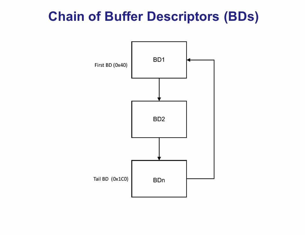
Chain of Buffer Descriptors (BDs)
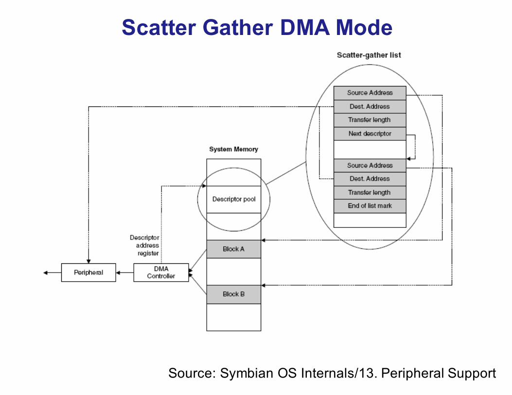
Scatter Gather DMA Mode
Source: Symbian OS Internals/13. Peripheral Support

What is the primary advantage of using a Scatter-Gather DMA Transfer
rather than a Simple DMA transfer?
Problem 18

Scatter Gather DMA Mode
Source: Symbian OS Internals/13. Peripheral Support
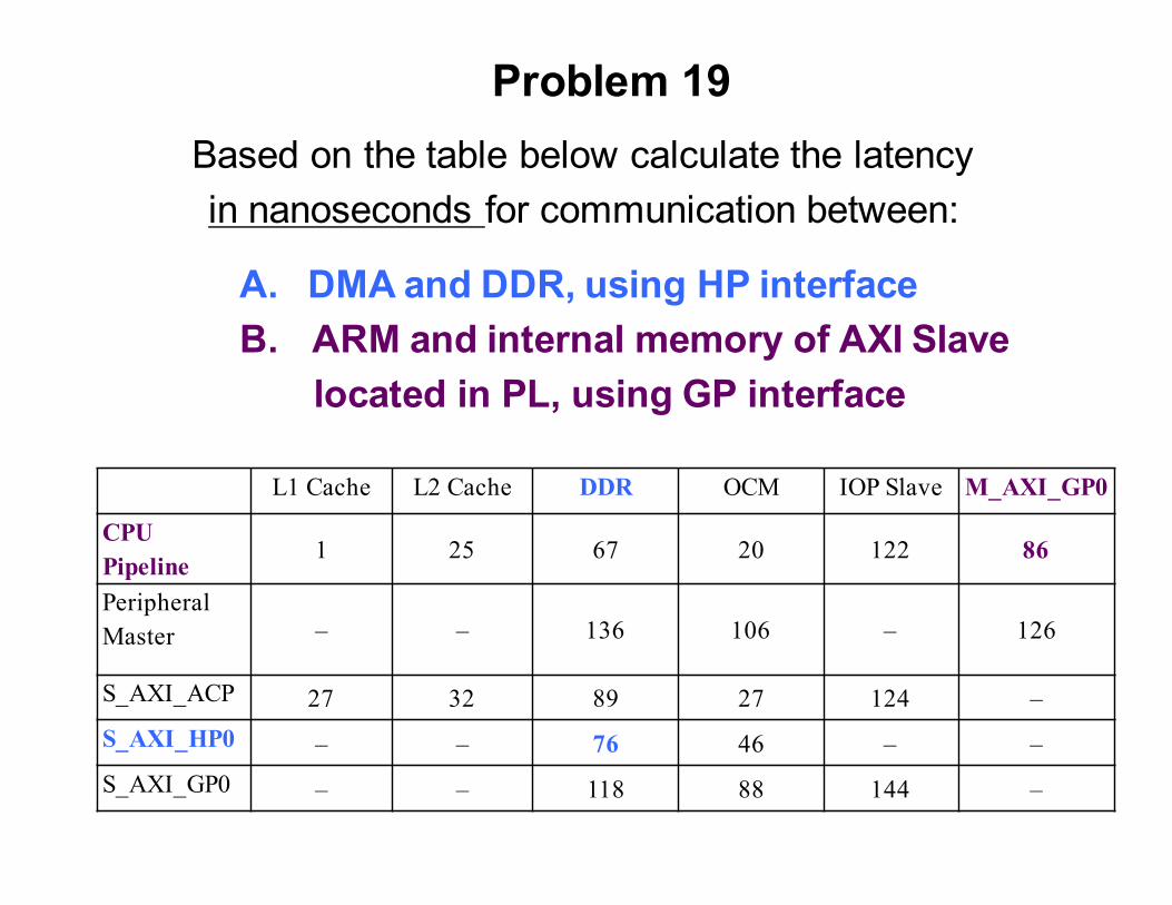
Based on the table below calculate the latencyin nanoseconds for communication between:
Problem 19
A. DMA and DDR, using HP interfaceB. ARM and internal memory of AXI Slave
located in PL, using GP interface
L1 Cache L2 Cache DDR OCM IOP Slave M_AXI_GP0
CPU Pipeline 1 25 67 20 122 86
Peripheral Master – – 136 106 – 126
S_AXI_ACP 27 32 89 27 124 –S_AXI_HP0 – – 76 46 – –S_AXI_GP0 – – 118 88 144 –

AXI Interconnects and Interfaces
Source: The Zynq Book
ACP - Accelerator Coherency Port SCU - Snoop Control Unit

• Processing system– CPU at 667 MHz (650 MHz on Zybo board)– DDR at 533 MHz – Programmable logic is running at 150 MHz
• Latency in terms of CPU clock cycles– S_AXI_HP at 76 CPU cycles is
17 cycles for the PL (114 ns)
CPU Clock Period = 1 / CPU Clock Frequency = 1.5 ns
A. 76 * 1.5 ns = 114 ns
B. 86 * 1.5 ns = 129 ns
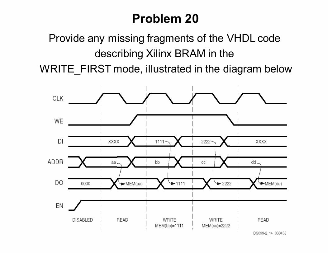
Provide any missing fragments of the VHDL code describing Xilinx BRAM in the
WRITE_FIRST mode, illustrated in the diagram below
Problem 20

60
Block RAM with synchronous read Write-First Mode - cont'darchitecture behavioral of raminfr is
type ram_type is array (0 to 2**r-1) of std_logic_vector (w-1 downto 0);
signal RAM : ram_type := (others => (others => '0'));
beginprocess (clk) beginif (clk'event and clk = '1') then
if (en = '1') thenif (we = '1') then
RAM(to_integer(unsigned(addr))) <= di;do <= di;
elsedo <= RAM(to_integer(unsigned(addr)));
end if; end if;
end if; end process;
end behavioral;
Explain the difference between Simple Dual Port RAM and True Dual Port RAM
Problem 21

62
Block RAM
Simple Dual Port (SDP) = one port for read, one port for write(write_A-read_B, read_A_write_B)
True Dual Port (TDP) =both ports can be used for read or write
(read_A-read_B, read_A-write_B, write_A-read_B, write_A-write_B)

List at least 3 primary differences between distributed RAM and Block RAM in Zynq
Problem 22
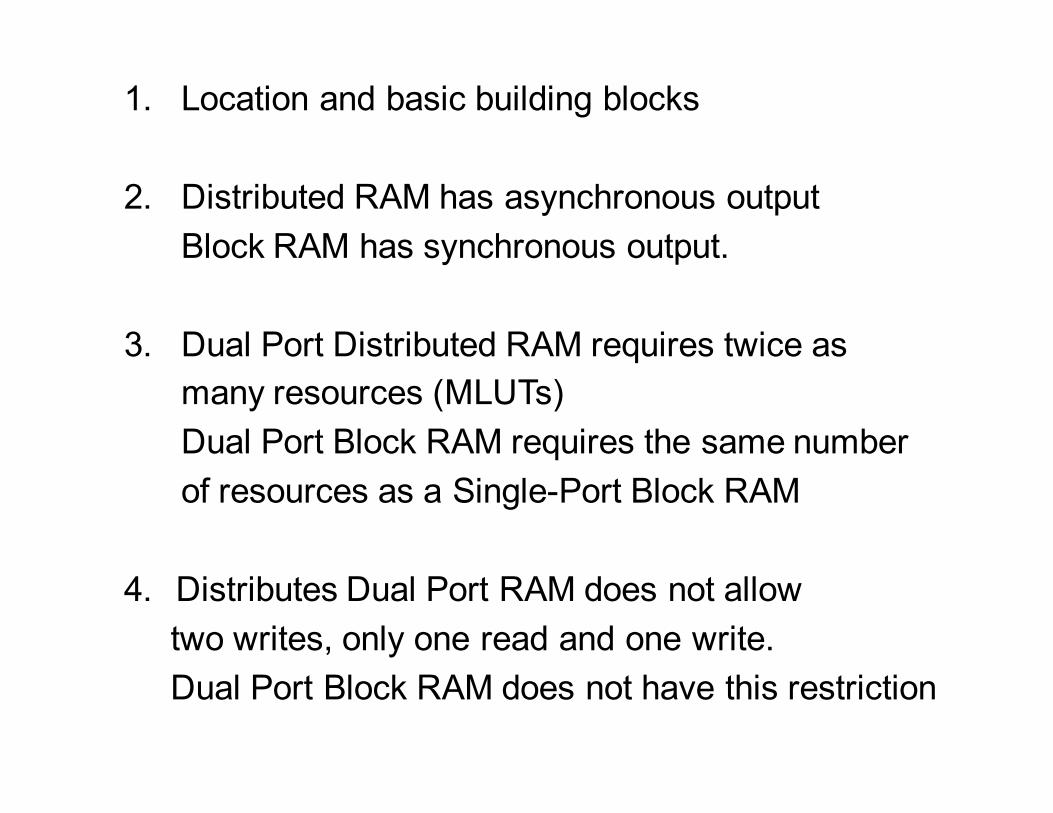
1. Location and basic building blocks
2. Distributed RAM has asynchronous outputBlock RAM has synchronous output.
3. Dual Port Distributed RAM requires twice asmany resources (MLUTs)Dual Port Block RAM requires the same numberof resources as a Single-Port Block RAM
4. Distributes Dual Port RAM does not allowtwo writes, only one read and one write.Dual Port Block RAM does not have this restriction

65
Location of Distributed RAMRAM blocks
Multipliers
Logic blocks
Graphics based on The Design Warrior’s Guide to FPGAsDevices, Tools, and Flows. ISBN 0750676043
Copyright © 2004 Mentor Graphics Corp. (www.mentor.com)
DSP unitsRAM blocks
Logic resources
Logic resources(CLB slices)

66
Location of Block RAMsRAM blocks
Multipliers
Logic blocks
Graphics based on The Design Warrior’s Guide to FPGAsDevices, Tools, and Flows. ISBN 0750676043
Copyright © 2004 Mentor Graphics Corp. (www.mentor.com)
DSP unitsRAM blocks
Logic resources
Logic resources(CLB slices)
67
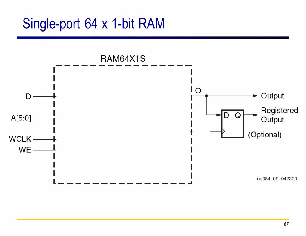
Single-port 64 x 1-bit RAM
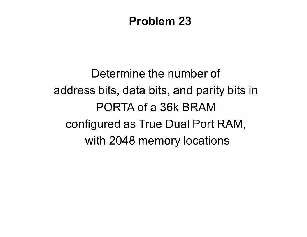
Determine the number of address bits, data bits, and parity bits in
PORTA of a 36k BRAM configured as True Dual Port RAM,
with 2048 memory locations
Problem 23

2048 = 211 => 11 address bits
36k / 2k = 18 => 16 data bits + 2 parity bits
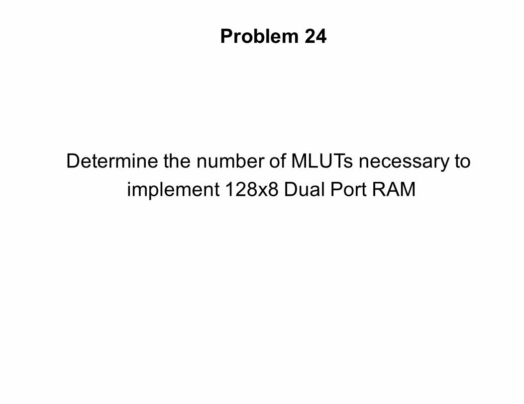
Determine the number of MLUTs necessary toimplement 128x8 Dual Port RAM
Problem 24
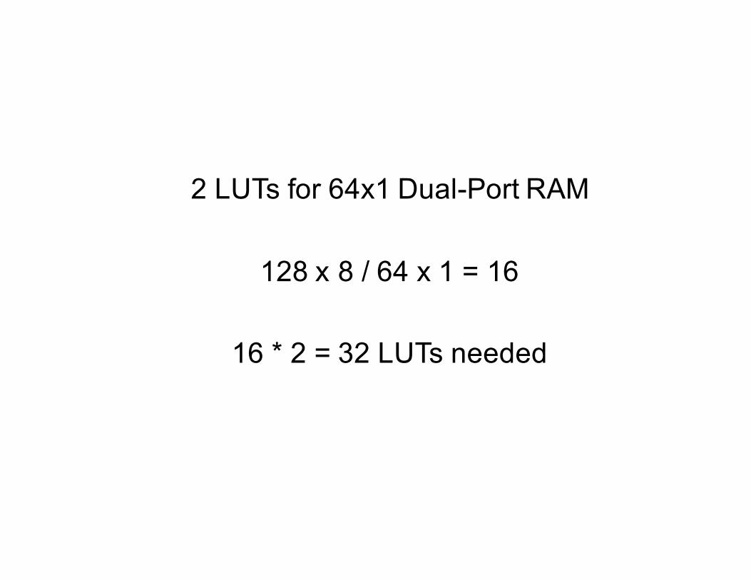
2 LUTs for 64x1 Dual-Port RAM
128 x 8 / 64 x 1 = 16
16 * 2 = 32 LUTs needed

Supplement the attached timing diagrams with the values of dout for
Problem 25
A. Standard FIFOB. B. First-Word Fall-Through FIFO

73
Operation of the “Standard” FIFO
−−−−− A B C D

74
Operation of the First-Word Fall-Through FIFO


