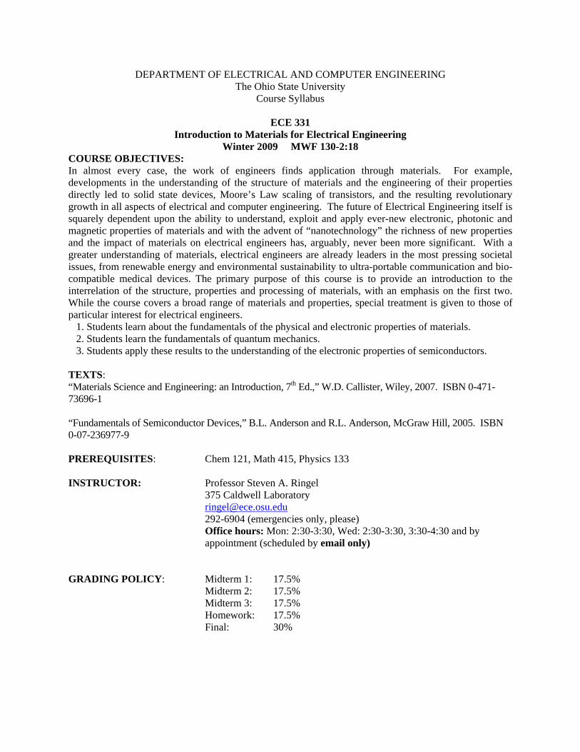
DEPARTMENT OF ELECTRICAL AND COMPUTER ENGINEERING The Ohio State University
Course Syllabus
ECE 331 Introduction to Materials for Electrical Engineering
Winter 2009 MWF 130-2:18 COURSE OBJECTIVES: In almost every case, the work of engineers finds application through materials. For example, developments in the understanding of the structure of materials and the engineering of their properties directly led to solid state devices, Moore’s Law scaling of transistors, and the resulting revolutionary growth in all aspects of electrical and computer engineering. The future of Electrical Engineering itself is squarely dependent upon the ability to understand, exploit and apply ever-new electronic, photonic and magnetic properties of materials and with the advent of “nanotechnology” the richness of new properties and the impact of materials on electrical engineers has, arguably, never been more significant. With a greater understanding of materials, electrical engineers are already leaders in the most pressing societal issues, from renewable energy and environmental sustainability to ultra-portable communication and bio-compatible medical devices. The primary purpose of this course is to provide an introduction to the interrelation of the structure, properties and processing of materials, with an emphasis on the first two. While the course covers a broad range of materials and properties, special treatment is given to those of particular interest for electrical engineers. 1. Students learn about the fundamentals of the physical and electronic properties of materials. 2. Students learn the fundamentals of quantum mechanics. 3. Students apply these results to the understanding of the electronic properties of semiconductors. TEXTS: “Materials Science and Engineering: an Introduction, 7th Ed.,” W.D. Callister, Wiley, 2007. ISBN 0-471-73696-1 “Fundamentals of Semiconductor Devices,” B.L. Anderson and R.L. Anderson, McGraw Hill, 2005. ISBN 0-07-236977-9 PREREQUISITES: Chem 121, Math 415, Physics 133 INSTRUCTOR: Professor Steven A. Ringel 375 Caldwell Laboratory [email protected] 292-6904 (emergencies only, please) Office hours: Mon: 2:30-3:30, Wed: 2:30-3:30, 3:30-4:30 and by appointment (scheduled by email only) GRADING POLICY: Midterm 1: 17.5% Midterm 2: 17.5% Midterm 3: 17.5% Homework: 17.5% Final: 30%
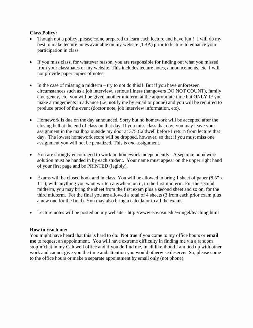
Class Policy: • Though not a policy, please come prepared to learn each lecture and have fun!! I will do my
best to make lecture notes available on my website (TBA) prior to lecture to enhance your participation in class.
• If you miss class, for whatever reason, you are responsible for finding out what you missed from your classmates or my website. This includes lecture notes, announcements, etc. I will not provide paper copies of notes.
• In the case of missing a midterm – try to not do this!! But if you have unforeseen
circumstances such as a job interview, serious illness (hangovers DO NOT COUNT), family emergency, etc, you will be given another midterm at the appropriate time but ONLY IF you make arrangements in advance (i.e. notify me by email or phone) and you will be required to produce proof of the event (doctor note, job interview information, etc).
• Homework is due on the day announced. Sorry but no homework will be accepted after the
closing bell at the end of class on that day. If you miss class that day, you may leave your assignment in the mailbox outside my door at 375 Caldwell before I return from lecture that day. The lowest homework score will be dropped, however, so that if you must miss one assignment you will not be penalized. This is one assignment.
• You are strongly encouraged to work on homework independently. A separate homework solution must be handed in by each student. Your name must appear on the upper right hand of your first page and be PRINTED (legibly).
• Exams will be closed book and in class. You will be allowed to bring 1 sheet of paper (8.5” x 11”), with anything you want written anywhere on it, to the first midterm. For the second midterm, you may bring the sheet from the first exam plus a second sheet and so on, for the third midterm. For the final you are allowed a total of 4 sheets (3 from each prior exam plus a new one for the final). You may also bring a calculator to all the exams.
• Lecture notes will be posted on my website - http://www.ece.osu.edu/~ringel/teaching.html
How to reach me: You might have heard that this is hard to do. Not true if you come to my office hours or email me to request an appointment. You will have extreme difficulty in finding me via a random stop’n’chat in my Caldwell office and if you do find me, in all likelihood I am tied up with other work and cannot give you the time and attention you would otherwise deserve. So, please come to the office hours or make a separate appointment by email only (not phone).
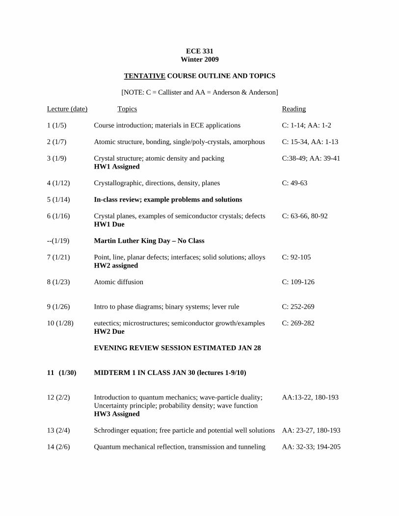
ECE 331 Winter 2009
TENTATIVE COURSE OUTLINE AND TOPICS
[NOTE: C = Callister and AA = Anderson & Anderson]
Lecture (date) Topics Reading 1 (1/5) Course introduction; materials in ECE applications C: 1-14; AA: 1-2 2 (1/7) Atomic structure, bonding, single/poly-crystals, amorphous C: 15-34, AA: 1-13 3 (1/9) Crystal structure; atomic density and packing C:38-49; AA: 39-41 HW1 Assigned 4 (1/12) Crystallographic, directions, density, planes C: 49-63 5 (1/14) In-class review; example problems and solutions 6 (1/16) Crystal planes, examples of semiconductor crystals; defects C: 63-66, 80-92 HW1 Due --(1/19) Martin Luther King Day – No Class 7 (1/21) Point, line, planar defects; interfaces; solid solutions; alloys C: 92-105
HW2 assigned
8 (1/23) Atomic diffusion C: 109-126 9 (1/26) Intro to phase diagrams; binary systems; lever rule C: 252-269 10 (1/28) eutectics; microstructures; semiconductor growth/examples C: 269-282 HW2 Due
EVENING REVIEW SESSION ESTIMATED JAN 28 11 (1/30) MIDTERM 1 IN CLASS JAN 30 (lectures 1-9/10) 12 (2/2) Introduction to quantum mechanics; wave-particle duality; AA:13-22, 180-193 Uncertainty principle; probability density; wave function HW3 Assigned 13 (2/4) Schrodinger equation; free particle and potential well solutions AA: 23-27, 180-193 14 (2/6) Quantum mechanical reflection, transmission and tunneling AA: 32-33; 194-205
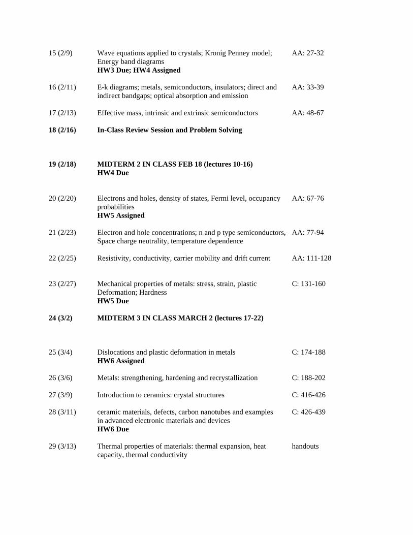
15 (2/9) Wave equations applied to crystals; Kronig Penney model; AA: 27-32 Energy band diagrams HW3 Due; HW4 Assigned 16 (2/11) E-k diagrams; metals, semiconductors, insulators; direct and AA: 33-39 indirect bandgaps; optical absorption and emission 17 (2/13) Effective mass, intrinsic and extrinsic semiconductors AA: 48-67 18 (2/16) In-Class Review Session and Problem Solving 19 (2/18) MIDTERM 2 IN CLASS FEB 18 (lectures 10-16) HW4 Due 20 (2/20) Electrons and holes, density of states, Fermi level, occupancy AA: 67-76 probabilities HW5 Assigned 21 (2/23) Electron and hole concentrations; n and p type semiconductors, AA: 77-94 Space charge neutrality, temperature dependence 22 (2/25) Resistivity, conductivity, carrier mobility and drift current AA: 111-128 23 (2/27) Mechanical properties of metals: stress, strain, plastic C: 131-160 Deformation; Hardness HW5 Due 24 (3/2) MIDTERM 3 IN CLASS MARCH 2 (lectures 17-22) 25 (3/4) Dislocations and plastic deformation in metals C: 174-188 HW6 Assigned 26 (3/6) Metals: strengthening, hardening and recrystallization C: 188-202 27 (3/9) Introduction to ceramics: crystal structures C: 416-426 28 (3/11) ceramic materials, defects, carbon nanotubes and examples C: 426-439 in advanced electronic materials and devices HW6 Due 29 (3/13) Thermal properties of materials: thermal expansion, heat handouts capacity, thermal conductivity


