
EBCP RoseRedBluetooth Development Platform User Guide
Copyright © 2002 ARM Limited. All rights reserved.ARM DUI 0190A

EBCP RoseRedBluetooth Development Platform User Guide
Copyright © 2002 ARM Limited. All rights reserved.
Release Information
Proprietary Notice
Words and logos marked with ® or ™ are registered trademarks or trademarks owned by ARM Limited, except as otherwise stated below in this proprietary notice. Other brands and names mentioned herein may be the trademarks of their respective owners.
Neither the whole nor any part of the information contained in, or the product described in, this document may be adapted or reproduced in any material form except with the prior written permission of the copyright holder.
The product described in this document is subject to continuous developments and improvements. All particulars of the product and its use contained in this document are given by ARM in good faith. However, all warranties implied or expressed, including but not limited to implied warranties of merchantability, or fitness for purpose, are excluded.
This document is intended only to assist the reader in the use of the product. ARM Limited shall not be liable for any loss or damage arising from the use of any information in this document, or any error or omission in such information, or any incorrect use of the product.
Confidentiality Status
This document is Open Access. This document has no restriction on distribution.
Product Status
The information in this document is final (information on a developed product).
Web Address
http://www.arm.com
Change history
Date Issue Change
April 24 2002 A New document
ii Copyright © 2002 ARM Limited. All rights reserved. ARM DUI 0190A
Conformance Notices
This section contains conformance notices.
Federal Communications Commission Notice
This device is test equipment and consequently is exempt from part 15 of the FCC Rules under section 15.103 (c).
CE Declaration of Conformity
The system should be powered down when not in use.
The Integrator generates, uses, and can radiate radio frequency energy and may cause harmful interference to radio communications. However, there is no guarantee that interference will not occur in a particular installation. If this equipment causes harmful interference to radio or television reception, which can be determined by turning the equipment off or on, you are encouraged to try to correct the interference by one or more of the following measures:
• ensure attached cables do not lie across the card
• reorient the receiving antenna
• increase the distance between the equipment and the receiver
• connect the equipment into an outlet on a circuit different from that to which the receiver is connected
• consult the dealer or an experienced radio/TV technician for help
Note It is recommended that wherever possible Shielded interface cables be used.
ARM DUI 0190A Copyright © 2002 ARM Limited. All rights reserved. iii

iv Copyright © 2002 ARM Limited. All rights reserved. ARM DUI 0190A

ContentsEBCP RoseRed Bluetooth Development Platform User Guide
PrefaceAbout this document .................................................................................... viiiFeedback ....................................................................................................... xi
Chapter 1 Introduction1.1 About the BDP ............................................................................................ 1-21.2 BDP system architecture ............................................................................. 1-41.3 About the Integrator/BTAP .......................................................................... 1-71.4 About the Integrator/BTLM ........................................................................ 1-13
Chapter 2 Getting Started2.1 Basic hardware setup ................................................................................. 2-22.2 Connecting power ....................................................................................... 2-52.3 System expansion ....................................................................................... 2-72.4 Building and downloading an image ........................................................... 2-82.5 Getting started with Bluetooth HCI Toolbox .............................................. 2-13
Chapter 3 Motherboard Hardware Description3.1 Motherboard FPGA ..................................................................................... 3-23.2 System bus ................................................................................................. 3-3
ARM DUI 0190A Copyright © 2002 ARM Limited. All rights reserved. v

Contents
3.3 Static memory interface .............................................................................. 3-93.4 Reset control ............................................................................................ 3-113.5 Motherboard clock controller .................................................................... 3-143.6 Interrupt controller .................................................................................... 3-163.7 Bluetooth peripherals ................................................................................ 3-17
Chapter 4 BTLM Hardware Description4.1 BTLM FPGAs ............................................................................................. 4-24.2 JTAG support ............................................................................................. 4-74.3 System bus interface ................................................................................ 4-114.4 BTLM clock control ................................................................................... 4-124.5 Reset control ............................................................................................ 4-144.6 BTLM LEDs and switches ........................................................................ 4-154.7 Audio CODEC interface ............................................................................ 4-164.8 Diagnostic connections ............................................................................. 4-174.9 CIF connector ........................................................................................... 4-18
Chapter 5 Programmer’s Reference5.1 System memory map description ............................................................... 5-25.2 Bluetooth UART .......................................................................................... 5-75.3 Bluetooth GPIO .......................................................................................... 5-85.4 Bluetooth interrupt controller ...................................................................... 5-95.5 Bluetooth system controller ...................................................................... 5-125.6 Motherboard peripherals .......................................................................... 5-13
Appendix A Connector PinoutsA.1 Motherboard connectors HDRA and EXPA ................................................ A-2A.2 Motherboard connector HDRB ................................................................... A-4A.3 Motherboard and BTLM connectors EXPB ................................................ A-6A.4 Expansion connector EXPM ....................................................................... A-9A.5 Serial interface connectors ....................................................................... A-11A.6 Multi-ICE (JTAG) ...................................................................................... A-12A.7 Diagnostic connectors .............................................................................. A-13
vi Copyright © 2002 ARM Limited. All rights reserved. ARM DUI 0190A
Preface
This preface introduces the ARM Bluetooth Development Platform (BDP) and its reference documentation. It contains the following sections:
• About this document on page viii
• Feedback on page xi.
ARM DUI 0190A Copyright © 2002 ARM Limited. All rights reserved. vii

Preface
About this document
This document provides a information about to how to set up and use the BDP.
Intended audience
This document has been written for experienced hardware and software engineers as an aid to using the BDP to develop ARM-based Bluetooth products. It assumes a working knowledge of ARM and other development tools that are used to develop applications for the ARM architecture.
Organization
This document is organized into the following chapters:
Chapter 1 Introduction
Read this chapter for an introduction to the BDP. This chapter identifies the main components, connectors, and indicators on the modules that go to form the BDP.
Chapter 2 Getting Started
Read this chapter for a description of how to set up and start using the BDP. This chapter describes how to attach the modules to one another, how to power-up, and how to load and run a program.
Chapter 3 Motherboard Hardware Description
Read this chapter for a description of the motherboard hardware. This includes clock generators, reset system, and peripherals.
Chapter 4 BTLM Hardware Description
Read this chapter for a description of the BTLM hardware. This chapter contains information about the FPGAs that contain the Ericsson Bluetooth Core (EBC) functions and how they are configured.
Chapter 5 Programmer’s Reference
Read this chapter for a description of the system memory map and control registers. The registers described in this chapter are those associated with controlling the BDP platform.
Appendix A Connector Pinouts
Read this appendix for a description of connector pinouts.
viii Copyright © 2002 ARM Limited. All rights reserved. ARM DUI 0190A

Preface
Typographical conventions
The following typographical conventions are used in this book:
italic Highlights important notes, introduces special terminology, denotes internal cross-references, and citations.
bold Highlights interface elements, such as menu names. Denotes ARM processor signal names. Also used for terms in descriptive lists, where appropriate.
monospace Denotes text that can be entered at the keyboard, such as commands, file and program names, and source code.
monospace Denotes a permitted abbreviation for a command or option. The underlined text can be entered instead of the full command or option name.
monospace italic Denotes arguments to commands and functions where the argument is to be replaced by a specific value.
monospace bold Denotes language keywords when used outside example code.
Further reading
This section lists related publications by ARM Limited and other companies that provide additional information.
ARM and ARM partner publications
The following publications provide information about related ARM Integrator products:
• ARM Integrator/CM7TDMI User Guide (ARM DUI 0126)
• ARM Integrator/LM-XCV400+ User Guide (ARM DUI 0130)
• ARM Integrator/LM-XCV600E+/EP20K600E+ User Guide (ARM DUI 0146)
• ARM Integrator/AM User Guide (ARM DUI 0133).
The following publication provides reference information about the EABBC:
• Example AMBA Bluetooth Baseband Controller (EABBC) Integration Manual (ARM DII 0007)
• Example AMBA Bluetooth Baseband Controller (EABBC) Technical Reference Manual (ARM DDI 0175).
The following publications provide reference information about ARM architecture:
• AMBA Specification (ARM IHI 0011)
ARM DUI 0190A Copyright © 2002 ARM Limited. All rights reserved. ix

Preface
• ARM Architectural Reference Manual (ARM DDI 0100).
The following publications provide information about the ARM Developer Suite:
• ADS Getting Started (ARM DUI 0064)
• ADS Compiler, Linker, and Utilities Guide (ARM DUI 0067)
• ADS Debuggers Guide (ARM DUI 0066)
• ADS Debug Target Guide (ARM DUI 0058)
• ADS Developer Guide (ARM DUI 0056)
• ADS CodeWarrior IDE Guide (ARM DUI 0065).
The following publication provides additional information about the BTLM Codec add-on board:
• BTLM Codec Add-on Board (EN/LZT 108 5570/30) Revision R1
Ericsson Technology Licensing AB.
The following publications provide information about Bluetooth HCI Toolbox:
• Bluetooth HCI Toolbox User’s Guide
Ericsson Mobile Communications AB.
Other publications
The following publication provides information about the clock controller chip used on the Integrator modules:
• MicroClock OSCaR User Configurable Clock Data Sheet (MDS525), MicroClock Division of ICS, San Jose, CA.
x Copyright © 2002 ARM Limited. All rights reserved. ARM DUI 0190A

Preface
Feedback
ARM Limited welcomes feedback both on the Bluetooth Development Platform and on the documentation.
Feedback on this document
If you have any comments about this document, please send email to [email protected] giving:
• the document title
• the document number
• the page number(s) to which your comments refer
• an explanation of your comments.
General suggestions for additions and improvements are also welcome.
Feedback on the BDP
If you have any comments or suggestions about this product, please contact your supplier giving:
• the product name
• an explanation of your comments.
ARM DUI 0190A Copyright © 2002 ARM Limited. All rights reserved. xi

Preface
xii Copyright © 2002 ARM Limited. All rights reserved. ARM DUI 0190A

Chapter 1 Introduction
This chapter introduces the Bluetooth Development Platform (BDP). It contains the following sections:
• About the BDP on page 1-2
• BDP system architecture on page 1-4
• About the Integrator/BTAP on page 1-7
• About the Integrator/BTLM on page 1-13.
ARM DUI 0190A Copyright © 2002 ARM Limited. All rights reserved. 1-1

Introduction
1.1 About the BDP
The Bluetooth Development Platform (BDP) is an Integrator-based development system designed to provide a flexible environment to enable rapid development of ARM-based Bluetooth devices. The BDP enables you to accurately model Bluetooth devices and to test communications between them.
The BDP comprises boards:
• Integrator/BTAP (BlueTooth ASIC Platform), referred to as the motherboard
• Integrator/BTLM (BlueTooth Logic Module).
These two boards are designed to be used with, for example, an Integrator/CM7TDMI core module. The core module and BTLM are plug-in modules that are mounted onto connectors on the motherboard. Figure 1-1 on page 1-3 shows the layout of the assembled BDP and core module.
1-2 Copyright © 2002 ARM Limited. All rights reserved. ARM DUI 0190A

Introduction
Figure 1-1 Assembled BDP with a core module
OF
F
12
34
CP
_V(I/O
)
-12V
12V5V
3V3
GN
D
OFF
1 2 3 4
BTLM Radio moduleIntegrator/7TDMIIntegrator/BTAP
ARM DUI 0190A Copyright © 2002 ARM Limited. All rights reserved. 1-3

Introduction
1.2 BDP system architecture
Figure 1-2 shows the architecture of the BDP fitted with an Integrator core module.
Figure 1-2 BDP system architecture
SSRAM FPGA(bus bridge/
SSRAM/SDRAMcontrollers)
FPGA(system control/
Bluetoothperipherals)
SDRAM
ARM core
Flash
BootROM
SRAM
System bus connectors
Peripheral input/output
HDRA/HDRB
Multi-ICE
Exp
ansi
on
CIFconnector
Lydiaconnector
Integrator/7TDMI
FPGA 1(AHB bus bridge/EBC functions)
FPGA 2(Multi channelPCM interface)
System bus connectors
EXPA/EXPB
BTLM
Integrator/BTAP
System bus (AHB)
GPIO (F bus)
EBI
RadiomoduleRadio
module CODEC
DIPswitches
DIPswitches
LEDs
LEDs
1-4 Copyright © 2002 ARM Limited. All rights reserved. ARM DUI 0190A

Introduction
The BDP design uses a modular architecture and shares the components of the EABBC architecture between the circuit boards as follows:
• the BTLM provides the EBC functions
• the core module provides the ARM7TDMI core, SSRAM, and SDRAM
• the motherboard provides system controller functions, the AMBA Advanced High-performance Bus (AHB) and Bluetooth peripherals.
In addition, you can also plug a standard Integrator logic module on top of the BTLM to add your own software and hardware IP to the system.
Although the BDP system is a functionally accurate Bluetooth system (see the EABBC Technical Reference Manual) there are some features of the Integrator platform that make it differ from the final ASIC implementation. These Integrator-specific features are as follows:
AHB bridge The AHB on the BDP is routed between FPGAs on each of the modules. This difference has no affect on the way that the EBC or Bluetooth peripherals function, but does affect the interface with the core.
The core module FPGA contains a bus bridge between the AHB system bus and the local memory bus on the core module. The bridge provides FIFOs for reads and writes in both directions. This introduces wait states for nonsequential accesses and means, for example, that the core accesses to peripherals are completed on the local memory bus side before being completed on the motherboard side. See the Integrator/CM7TDMI User Guide for more details.
AHB decoder
To ensure reliable operation when different combination of modules are attached, the Integrator uses a distributed bus decoding scheme. The bus decoder in the motherboard FPGA decodes all on-board addresses but only decodes regions for core and logic modules. The FPGA in each module provides a decoder for its own address space and supplies the appropriate bus responses (see System bus on page 3-3).
Clocks The AHB system bus and local memory bus on the core module are clocked separately. That is, the two buses are asynchronous. The system controller FPGA on the motherboard supplies the clocks for the AHB (including the AHB sides of the core module bus bridge) and for the BTLM. The core module generates its own clock for the local memory bus.
ARM DUI 0190A Copyright © 2002 ARM Limited. All rights reserved. 1-5

Introduction
Memory The BDP does not have a Static Memory Controller (SMC) but instead provides an Static Memory Interface (SMI) located at a different address (see System memory map description on page 5-2). The EBI provides access to the onboard boot, ROM, SSRAM, and flash.
1-6 Copyright © 2002 ARM Limited. All rights reserved. ARM DUI 0190A

Introduction
1.3 About the Integrator/BTAP
Figure 1-3 on page 1-8 shows the top of the motherboard. The motherboard is a variant of the standard Integrator/AP that uses a different FPGA configuration. The FPGA is configured to support Bluetooth, and does not provide support for PCI.
The main components provided by the motherboard are:
• System controller FPGA providing:
— AMBA Advanced High-performance Bus (AHB) with interfaces to the core and logic module
— AHB arbiter
— primary AHB bus decoder
— two UARTs
— General Purpose Input/Output (GPIO) controller
— three general-purpose counter timers
— watchdog timer
— reset controller
— system status and control registers.
• Clock generators supplying:
— system bus clocks
— UARTs clocks
— the counter-timers.
• Three types of memory:
— bootROM
— 32MB of 32-bit wide flash
— 512KB of 32-bit wide SSRAM.
Reads from and writes to the flash memory, bootROM, and SSRAM are controlled by the SMI. The FPGA provides write-protection for the flash memory.
Note The Integrator/BTAP is based on the standard Integrator/AP product and has a number of PCI components and connectors fitted. However, the PCI functions are not supported by the FPGA configuration supplied with the BDP.
ARM DUI 0190A Copyright © 2002 ARM Limited. All rights reserved. 1-7

Introduction
Figure 1-3 Integrator/BTAP layout
OF
F
12
34
CP
_V(I/O
)
-12V
12V5V
3V3
GN
D
Standbybutton
Resetbutton
Serial interfaceconnectors(J14, J15)
Keyboard/mouseconnectors (J16)
Alphanumericdisplay
Externalalpha display
connector (J12)
4-pole DIPswitch
System controllerFPGA
Core moduleconnector(HDRA)
System bus - PCIbridge
PCI expansionslots
(J9, J10, J11)
PCI-PCIbridge
CompactPCIconnectors
(J1, J2)
CompactPCIarbiter PLD
PCI arbiter PLD Power connector (J21)(for bench powered use)
External businterface connector
(EXPM)
Logic moduleconnector(EXPB)
Logic moduleconnector(EXPA)
Boot ROM
Core moduleconnector(HDRB)
ATX powerconnector
(J3)
Flash memory
SRAM
Debugconnectors(J23, J24)
AutoPCconnector
(J20)
Resetconnector
(J4)
Power-upconnector
(J13)
Power LEDconnector
(J22)
FPGA OKconnector
(J8)
ATX Case
1-8 Copyright © 2002 ARM Limited. All rights reserved. ARM DUI 0190A

Introduction
1.3.1 Motherboard connector summary
This section provides a summary of the connectors on the motherboard. These are illustrated in Figure 1-3 on page 1-8 and shown in Table 1-1.
Connector pinouts and signal descriptions are provided in Appendix A Connector Pinouts.
Table 1-1 Connector summary
Legend Function
J1 and J2 PCI backplane connectors.
J3 PC ATX type power supply input.
J4 Reset. Can be connected to a panel mounted push button.
J5 and J6 Logic module connectors EXPA and EXPB.
J7 Expansion module connector EXPM.
J8 FPGA OK. Can be connected to a panel mounted LED to function as a System OK indicator.
J9, J10, and J11 PCI local bus expansion (function not supported in this implementation).
J12 Alphanumeric display extension. Can be connected to a panel mounted alphanumeric display.
J13 Power button. Can be connected to a panel mounted push button.
J14 and J15 Serial channels 1 and 2.
J16 Mouse (top) Keyboard (lower).
J18 and J19 Core module connectors HDRA and HDRB.
J20 Not used.
J21 Power supply input. Can be used to connect power from a bench power supply.
J22 Power LED. Can be connected to a panel mounted LED to function as a Power ON indicator.
J23 Not used.
J24 Not used.
ARM DUI 0190A Copyright © 2002 ARM Limited. All rights reserved. 1-9

Introduction
1.3.2 Motherboard LEDs summary
The motherboard LEDs are shown in Figure 1-4.
Figure 1-4 Motherboard LED locations
The functions of the motherboard LEDs are summarized in Table 1-2.
3V35V
12V
LED0LED1
LED2
LED3
CP
_V(I/O
)
-12V
12V5V
3V3
GN
D
Standby
ATX Case
FPGA OK
Table 1-2 Motherboard LED functional summary
LED Color Function
LED0 Green This LED is controlled by writing to bit 0 in the AP_LEDS register.
LED1 Yellow This LED is controlled by writing to bit 1 in the AP_LEDS register.
LED2 Red This LED is controlled by writing to bit 2 in the AP_LEDS register.
1-10 Copyright © 2002 ARM Limited. All rights reserved. ARM DUI 0190A

Introduction
The AP_LEDS register is described in LED control and boot switch registers on page 5-13.
LED3 Green This LED is controlled by writing to bit 3 in the AP_LEDS register.
3V3 Green Indicates that a 3.3V supply is available.
5V Green Indicates that a 5V supply is available.
12V Green Indicates that a +12V supply is available.
STANDBY Red Indicates that power supply unit connected to the ATX power connector is in standby mode. To power on the BDP, press the POWER button.
FPGA OK Green Indicates that the system controller FPGA has successfully loaded its configuration data following power on.
Table 1-2 Motherboard LED functional summary (continued)
LED Color Function
ARM DUI 0190A Copyright © 2002 ARM Limited. All rights reserved. 1-11

Introduction
1.3.3 Motherboard test points
The motherboard provides five test points as an aid to diagnostics. These are shown in Figure 1-5.
Figure 1-5 Test points
The functions of the test points are shown in Table 1-3.
TP5 TP3
TP1TP2TP4
Table 1-3 Test point functions
Test point Signal Function
TP1 CLK24MHZ Crystal oscillator output
TP2 UARTCLK UART clock input to the system controller
TP3 SYSCLK System bus clock crystal oscillator output
TP4 - Not used for BDP
TP5 nSYSRST Reset signal
1-12 Copyright © 2002 ARM Limited. All rights reserved. ARM DUI 0190A
Introduction
1.4 About the Integrator/BTLM
Figure 1-6 on page 1-14 shows the top view of the BTLM.
The BTLM provides all of the Bluetooth functionality except for the peripherals and SMI. The main components on the BTLM are:
• two Altera Apex FPGAs
• audio COder/DECoder (CODEC)
• Multi-ICE and RF module connectors.
• Cable Interface Connector (CIF).
These components are described in Chapter 4 BTLM Hardware Description.
1.4.1 BTLM connector summary
This section provides a summary of the connectors on the BTLM. These are illustrated in Figure 1-6 on page 1-14 and shown in Table 1-4.
Connector pinouts are provided in Appendix A Connector Pinouts.
Table 1-4 Connector summary
Legend Function
J25 and J26 EXPA and EXPB module connectors.
J27 and J28 EXPA and EXPB motherboard connectors (fitted to the underside).
J30 Multi-ICE connector.
J31 and J32 RF module connectors.
J33 Download connector for use with Altera FPGA tools.
J34 Audio CODEC interface.
J35, J36, J37, and J38
Debug connectors (reserved for production test).
J39 CIF connector. This is used to connect one BTLM to another using a 20-way ribbon cable.
ARM DUI 0190A Copyright © 2002 ARM Limited. All rights reserved. 1-13

Introduction
Figure 1-6 BTLM layout (top)
OFF
1 2 3 4
Userpushbutton
CIFconnector
(J39)
Mode switches(SW2)
Module/motherboardconnector(EXPB)
Module/motherboardconnector
(EXPA)
Multi-ICEconnector
(J30)
CONFIGlink
Audio CODECinterface
(J34)
Systemstatus LEDs
Downloadconnector
(J33)
EBC statusLEDs
ConfigurationFlash
Lydiainterface
RF moduleinterface
(J31, J32)
FPGA1
FPGA2
1-14 Copyright © 2002 ARM Limited. All rights reserved. ARM DUI 0190A

Introduction
1.4.2 BTLM LEDs summary
The BTLM has two sets of status LEDs, as shown in Figure 1-7:
• System status LEDs on page 1-16
• EBC status LEDs on page 1-16.
Figure 1-7 BTLM LEDS
FPGA_OK
POWER
CFGLED
EBC StatusLEDs
ARM DUI 0190A Copyright © 2002 ARM Limited. All rights reserved. 1-15
Introduction
System status LEDs
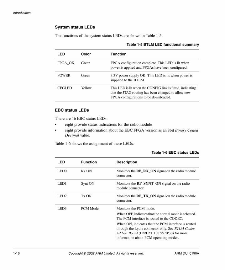
The functions of the system status LEDs are shown in Table 1-5.
EBC status LEDs
There are 16 EBC status LEDs:
• eight provide status indications for the radio module
• eight provide information about the EBC FPGA version as an 8bit Binary Coded Decimal value.
Table 1-6 shows the assignment of these LEDs.
Table 1-5 BTLM LED functional summary
LED Color Function
FPGA_OK Green FPGA configuration complete. This LED is lit when power is applied and FPGAs have been configured.
POWER Green 3.3V power supply OK. This LED is lit when power is supplied to the BTLM.
CFGLED Yellow This LED is lit when the CONFIG link is fitted, indicating that the JTAG routing has been changed to allow new FPGA configurations to be downloaded.
Table 1-6 EBC status LEDs
LED Function Description
LED0 Rx ON Monitors the RF_RX_ON signal on the radio module connector.
LED1 Synt ON Monitors the RF_SYNT_ON signal on the radio module connector.
LED2 Tx ON Monitors the RF_TX_ON signal on the radio module connector.
LED3 PCM Mode Monitors the PCM mode.
When OFF, indicates that the normal mode is selected. The PCM interface is routed to the CODEC.
When ON, indicates that the PCM interface is routed through the Lydia connector only. See BTLM Codec Add-on Board (EN/LZT 108 5570/30) for more information about PCM operating modes.
1-16 Copyright © 2002 ARM Limited. All rights reserved. ARM DUI 0190A

Introduction
LED4 AntSw ON Monitors the RF_ANT_SW signal on the radio module connector.
When OFF, the radio module uses its on-board antenna.
When ON, the radio module uses an antenna connected to its mini-coaxial connector.
LED5 CIF Mode Monitors the CIF mode.
When OFF, indicates that normal mode is selected. Tx and Rx are routed through the radio module
When ON, indicates that the cable baseband to baseband mode is selected. Tx and Rx are routed through the cable interface.
LED6 Phd OFF Monitors the RF_PHD_OFF signal on the radio module connector.
LED7 Px ON Monitors the RF_PX_ON signal on the radio module connector.
LED8 EBC_VER7 EBC FPGA version bit 7 (MSB)
LED9 EBC_VER6 EBC FPGA version bit 6
LED10 EBC_VER5 EBC FPGA version bit 5
LED11 EBC_VER4 EBC FPGA version bit 4
LED12 EBC_VER3 EBC FPGA version bit 3
LED13 EBC_VER2 EBC FPGA version bit 2
LED14 EBC_VER1 EBC FPGA version bit 1
LED15 EBC_VER0 EBC FPGA version bit 0 (MSB)
Table 1-6 EBC status LEDs (continued)
LED Function Description
ARM DUI 0190A Copyright © 2002 ARM Limited. All rights reserved. 1-17

Introduction
1-18 Copyright © 2002 ARM Limited. All rights reserved. ARM DUI 0190A

Chapter 2 Getting Started
This chapter describes how to prepare and start using the BDP. It contains the following sections:
• Basic hardware setup on page 2-2
• Connecting power on page 2-5
• System expansion on page 2-7
• Building and downloading an image on page 2-8
• Getting started with Bluetooth HCI Toolbox on page 2-13.
ARM DUI 0190A Copyright © 2002 ARM Limited. All rights reserved. 2-1

Getting Started
2.1 Basic hardware setup
Figure 2-1 shows an assembled system.
Figure 2-1 Assembled BDP
The steps required to set up the BDP hardware are as follows:
1. To mount the core module and BTLM onto the motherboard:
a. Place the motherboard on a firm level surface.
b. Align the connectors on each module with the corresponding connectors on the motherboard.
c. Press firmly on both ends of the module so that both connectors close together at the same time.
Ensure that you:
• mount the core module onto the connectors HDRA and HDRB
• mount the BTLM onto the connectors EXPA and EXPB.
Integrator/CM7TDMI
Integrator/BTLM
Integrator/BTAP
Radio module
2-2 Copyright © 2002 ARM Limited. All rights reserved. ARM DUI 0190A

Getting Started
2. Install the radio module onto the BTLM.
3. Set the DIP switches:
• On the motherboard set the DIP switches as shown in Table 2-1 (where x = don’t care).
• On the BTLM set the DIP switches to OFF (see BTLM switches on page 4-15 for details of the switch settings).
4. Connect the BDP to a PC running the Bluetooth HCI Toolbox and Multi-ICE as shown in Figure 2-2 on page 2-4:
• connect serial channel 1 (marked SERIAL A) on the motherboard to the COMs channel on the PC assigned to Bluetooth HCI Toolbox
• connect a Multi-ICE unit to the Multi-ICE connector on the core module.
5. Optionally connect a telephone handset to the Audio CODEC interface connector on the BTLM (see Audio CODEC interface on page 4-16).
6. Connect power to the BDP as described in Connecting power on page 2-5.
Table 2-1 Motherboard DIP switch settings
Switch Setting Function
S1[1] OFF Code jumps to 0x24 following reset and displays BT on the alphanumeric display
ON Code jumps to flash following reset and displays fL on the alphanumeric display
S1[2] x -
S1[3] x -
S1[4] x -
ARM DUI 0190A Copyright © 2002 ARM Limited. All rights reserved. 2-3

Getting Started
Figure 2-2 Equipment connections
OF
F
12
34
Bluetooth HCI Toolbox
Telephone handset
Multi-ICE
2-4 Copyright © 2002 ARM Limited. All rights reserved. ARM DUI 0190A
Getting Started
2.2 Connecting power
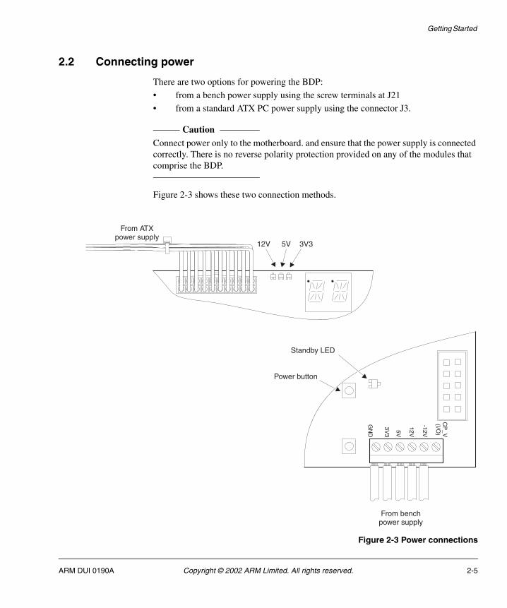
There are two options for powering the BDP:
• from a bench power supply using the screw terminals at J21
• from a standard ATX PC power supply using the connector J3.
Caution Connect power only to the motherboard. and ensure that the power supply is connected correctly. There is no reverse polarity protection provided on any of the modules that comprise the BDP.
Figure 2-3 shows these two connection methods.
Figure 2-3 Power connections
5V
3V3
GN
D
CP
_V(I/O
)
-12V
12V5V
3V3
GN
D
Power button
Standby LED
From benchpower supply
3V35V12V
From ATXpower supply
ARM DUI 0190A Copyright © 2002 ARM Limited. All rights reserved. 2-5

Getting Started
Power the BDP as follows:
1. Connect a power supply using one of the methods illustrated in Figure 2-3 on page 2-5.
2. Switch ON the AC supply to the power supply.
If you are using a bench power supply connected to J21, the BDP powers up immediately.
If you are using an ATX power supply connected to J3, the standby LED illuminates. Press the power button to power up the BDP development system.
Note
The BDP only require 3.3V and 5V. If you add modules that require 12V and –12V supplies, connect these supplies to the motherboard.
When you power up for the first time, the BDP runs a series of hardware self-tests and then jumps to 0x24 or to flash, depending on the setting of the motherboard DIP switch S2-1 (see Motherboard DIP switch settings on page 2-3). The characters BT or fL are displayed on the alphanumeric display.
2-6 Copyright © 2002 ARM Limited. All rights reserved. ARM DUI 0190A

Getting Started
2.3 System expansion
You can expand the BDP in two ways. By adding:
• an Integrator/LM logic module
• an Integrator/AM analyzer module.
The BDP provides memory map and bus arbitration support for an additional Integrator/LM logic module. You can use this to add custom devices to the system and can incorporate one AHB system bus master. The logic module must only be added to the EXPA/EXPB on top of the BTLM, as shown in Figure 2-4.
Figure 2-4 BDP expanded with an Integrator/LM logic module
Integrator analyzer modules can also be added to the top of the logic module or core module stack. The Integrator/AM does not impose loading on the signals coming up through the stack and can be used to connect a logic analyzer.
Integrator/CM7TDMI
Integrator/LM
Integrator/BTLM
Integrator/BTAP
Radio module
ARM DUI 0190A Copyright © 2002 ARM Limited. All rights reserved. 2-7

Getting Started
2.4 Building and downloading an image
The BDP is supplied with example the ADS project files:
• Products/HciFw/Build/HciFw.mcp
• Products/TestSample/Build/Client/Client.mcp
• Products/TestSample/Build/Server/Server.mcp
You can use these to build an hosted or embedded image to download to the BDP to get it up and running.
To build and download an image you require:
• a PC running CodeWarrior IDE, AXD, and Multi-ICE
• a Multi-ICE unit connected to the Multi-ICE connector on the core module and the parallel port of the PC running AXD.
To test the embedded images you also require:
• Two PCs, each running a terminal-emulation program such as HyperTerminal.
• Two development boards. If you use the flash versions of the Client.mcp and Server.mcp projects, you require only one Multi-ICE unit because you can load the images to each board individually.
Note
For more information on configuring and building Bluetooth applications, see the section on software configuration in the EABBC Software Integration User Guide.
2.4.1 Building a hosted system
Use CodeWarrior IDE to build the program and then download it to the BDP using Multi-ICE. The project offers the following different flash and nonflash build variants:
Debug These provide full debugging information but provide no optimization.
DebugRel and DebugRelFlash
These provide full debugging information and full optimization.
ReleaseFlash
These provide no debugging information and are fully optimized. These are the most compact versions intended to be used on the final ASIC implementation of the EABBC.
2-8 Copyright © 2002 ARM Limited. All rights reserved. ARM DUI 0190A

Getting Started
The flash variants are written to flash on the BDP and are retained during power down or reset. The nonflash variants are written into SDRAM on the core module and are lost when the BDP is powered down or reset.
To build and download a project:
1. Using CodeWarriorIDE, load the Hcifw.mcp project.
2. Select the required build variant and select Make from the Project menu.
3. Select Debug or Run from the Project menu.
Flash variants are automatically downloaded into flash memory.
4. Run the image using Multi-ICE or alternatively, for flash variants only, press the reset button.
2.4.2 Building an embedded system
Use CodeWarrior IDE to build the client and server programs and then download them to the BDPs using Multi-ICE. The project offers the following different flash and nonflash build variants:
Debug Use to debug a a server or client from flash with full code optimization.
DebugRel and DebugRelFlash
Use to debug a server or client with full code optimization.
ReleaseFlash
Use to debug a server or client from flash with full code optimization.
To build and download the project:
1. Using CodeWarriorIDE, load the Server.mcp project.
2. Select one of the server or client build variants and select Make from the Project menu.
3. Download the server application to one of your development boards.
4. Using CodeWarriorIDE, load the Client.mcp project.
5. Select one of the client build variants and select Make from the Project menu.
6. Download the client application to your second development board.
ARM DUI 0190A Copyright © 2002 ARM Limited. All rights reserved. 2-9

Getting Started
Running the test sample application
To check that the Bluetooth RF interfaces are functioning correctly, download and run the build variants of the Client.mcp and Server.mcp projects on two development boards.
Figure 2-5 The test sample application
Note These instructions are provided for convenience only. Refer to the Ericsson Bluetooth Test Sample Application User Guide (EN/LZT 108 5264) for full details and any changes to the application.
Run the communication tests as follows:
1. Set up two terminals. For example, use two PCs each running HyperTerminal.
2. Connect the terminals to the serial ports to UART0 of each board (the same UART labeled Bluetooth HCI Toolbox in Figure 2-2 on page 2-4).
3. Configure each HyperTerminal with the following settings:
• Baud rate: 57600
• Data bits: 8
• Parity: None
• Stop bits: 1
• Flow control: None
• Communication port: Set to the PC serial port being used.
4. Build and download the images.
Server
terminal
Client
terminal
BDP1 BDP2
Running a server
project
Running a client
project
Bluetooth
RF
Serial cable to
UART0
Serial cable to
UART0
2-10 Copyright © 2002 ARM Limited. All rights reserved. ARM DUI 0190A

Getting Started
5. Run the images using Multi-ICE units or alternatively, for flash variants only, press the reset button on the development boards.
Note Start the server application before starting the client application.
The HyperTerminal connected to the server board displays the information shown in Example 2-1.
Example 2-1 Initial HyperTerminal output from server
Server application logging.
6. Start the client application.
The HyperTerminal connected to the client board displays the information shown in Example 2-2.
Example 2-2 Initial HyperTerminal output from client
Client application logging.Sessions OK : 0 Inquiry failed : 0 Connections failed : 0 Disconnection failed : 0 Tx data failed : 0 No server reply : 0
7. The HyperTerminal connected to the client board continues to display the result of exchanges and increments the Sessions OK count as shown in Example 2-3. Occasionally one of the transactions might fail, and one of the failed counts increments instead.
Example 2-3 Ongoing HyperTerminal output from client
Who are you?headsetSessions OK : 1 Inquiry failed : 0 Connections failed : 0
ARM DUI 0190A Copyright © 2002 ARM Limited. All rights reserved. 2-11

Getting Started
Disconnection failed : 0 Tx data failed : 0 No server reply : 0
2-12 Copyright © 2002 ARM Limited. All rights reserved. ARM DUI 0190A

Getting Started
2.5 Getting started with Bluetooth HCI Toolbox
Bluetooth HCI Toolbox is a GUI-based application that runs on a PC. It enables you to send command packets to the EBC hardware during development, such as commands for configuring Bluetooth devices and setting up communications between them.
Bluetooth HCI Toolbox can be used for the following:
• Activating Bluetooth communications
• Setting the board address on page 2-14
• Setting XOtrim on page 2-14.
To prepare the BDP for Bluetooth communications using the hosted version of the software:
1. Build and download a DebugRel variant of the HciFw.mcp project (see Building and downloading an image on page 2-8.
2. Run the image using Multi-ICE or alternatively, for the flash variant only, press the reset button on the motherboard.
2.5.1 Activating Bluetooth communications
To activate Bluetooth communications:
1. Launch Bluetooth HCI Toolbox.
2. Check that the BDP has the correct board address set up. In the main window:
a. Click on Settings button in the static area, and then click on Read and use Current BD_ADDR.
b. In the displayed dialog box, check that the BD-ADDR parameter for each board is correct:
• If the addresses are correct, click OK.
• If one or both of the addresses are incorrect, change the board address, as described in Setting the board address on page 2-14.
3. Click the Basic Settings to 1 (or 2) button. This sets up polling.
4. Set up the radio link to another Bluetooth device:
a. Click the Link Control tab, then the Create ACL Connection button.
b. For each board number, check that the parameters are correctly set.
ARM DUI 0190A Copyright © 2002 ARM Limited. All rights reserved. 2-13

Getting Started
2.5.2 Setting the board address
To change the board address:
1. Click the Ericsson Specific tab, then the Firmware tab, and then the Ericsson Specific Write BD_ADDR button.
2. For each board number, change the addresses as required and then click Send.
3. Send an HCI reset command.
2.5.3 Setting XOtrim
Set the XO trim parameter as follows:
1. Click the Ericsson Specific tab, then the Radio tab and then the Write XO Trim button.
2. For each board, confirm or enter the correct value for the parameter and click Send.
3. Send an HCI reset command.
2-14 Copyright © 2002 ARM Limited. All rights reserved. ARM DUI 0190A

Chapter 3 Motherboard Hardware Description
This chapter describes the motherboard hardware. It contains the following sections:
• Motherboard FPGA on page 3-2
• System bus on page 3-3
• Static memory interface on page 3-9
• Reset control on page 3-11
• Motherboard clock controller on page 3-14
• Interrupt controller on page 3-16
• Bluetooth peripherals on page 3-17.
ARM DUI 0190A Copyright © 2002 ARM Limited. All rights reserved. 3-1

Motherboard Hardware Description
3.1 Motherboard FPGA
The motherboard FPGA provides system control and interface functions, as illustrated in Figure 3-1. These include:
• system bus interface and arbiter
• Static Memory Interface (SMI)
• reset controller
• clock rate registers
• Bluetooth interrupt controller
• three counter timers and a watchdog timer
• two Bluetooth UARTs
• Bluetooth General Purpose Input/Output (GPIO) port
• LED driver and boot switch reader.
Figure 3-1 Motherboard FPGA functional block diagram
������������ ����������
��������������������
������� �����
�����������������������
�������������
��������� �!"#�$%
����������&���&������������
����������������&�����������
���
����� ��� ����
!����������
������������&������&��'�����������&�����&��
(���)���������
���
*���
��!�+
����!�+
(���)��������������
3-2 Copyright © 2002 ARM Limited. All rights reserved. ARM DUI 0190A

Motherboard Hardware Description
3.2 System bus
The system bus provided by the motherboard is an AMBA AHB implementation. This is used to interface between the motherboard and the:
• Integrator/CM7TDMI core module plugged into the HDRA/HDRB stack
• BTLM and an optional logic module plugged into the EXPA/EXPB stack.
3.2.1 Bus architecture
The system has four main buses that are routed between system controller FPGA on the motherboard and the FPGAs on modules. These are shown in Figure 3-2 with their generic names.
Figure 3-2 System bus architecture
����������
���������
�� ����� ����������
���������������
���������
��������� ���������
���������
�������
�������
������
������
�� �������
ARM DUI 0190A Copyright © 2002 ARM Limited. All rights reserved. 3-3

Motherboard Hardware Description
3.2.2 HDRA/EXPA signals
The HDRA and EXPA connectors carry four buses between the motherboard and the modules. The Generic name column refers to the connector pin identities shown in Appendix A Connector Pinouts.
The buses are implemented on Integrator as follows:
A[31:0] This is the address bus and is connected between the system controller FPGAs on the motherboard and the FPGAs each module.
B[31:0] This bus does not connect to the system controller FPGA on the motherboard, but does connect HDRA to EXPA. Core modules that use Virtex FPGAs and logic modules also have pins connected to this bus.
The B[31:0] signals can be used, for example, to implement a bus between two logic modules because they are not driven by the system controller FPGA.
C[31:0] The upper half of this bus C[31:16] is spare. The lower half C[15:0] is used to implement a system control bus, as described in Control bus on page 3-6.
D[31:0] This is the data bus and is connected between the FPGAs on the motherboard and on each module. The AHB on Integrator differs from the AMBA standard in that it uses a bidirectional bus HDATA rather than HWDATA and HRDATA. It is impractical to implement two unidirectional buses at board level due to the high number of connections required on each module. The tristate HDATA bus is used to model the multiplexors that you normally implement on an ASIC.
Inside the FPGAs, the bidirectional bus is demultiplexed so that standard AHB masters and slaves can be implemented.
Table 3-1 System buses
Generic name Signal name Description
A[31:0] HADDR[31:0] System address bus
B[31:0] Reserved Spare system bus
C[31:0] - System control bus
D[31:0] HDATA[31:0] System data bus
GPIO[31:0] - Interconnect bus
3-4 Copyright © 2002 ARM Limited. All rights reserved. ARM DUI 0190A

Motherboard Hardware Description
GPIO[31:0] This bus provides interconnections between the motherboard FPGA and the FPGAs on the BTLM. The lower half of this bus GPIO[15:0] is assigned to the GPIO ports (see GPIO on page 3-20) and the upper half are used for a number of control signals for the EBC. The assignment of the GPIO signals is shown in Table 3-2
3.2.3 HDRB/EXPB signals
The HDRB and EXPB connectors are used to connect a number of system bus control, Integrator system, and JTAG signals. The full pinout is given in Appendix A Connector Pinouts. The Integrator-specific signals or those implemented in an Integrator-specific way are as follows:
Motherboard detect (nMBDET)
If the motherboard detect (nMBDET) is LOW then the module at the bottom of the stack routes the JTAG signals down to the motherboard. It is important that TDI is looped back to TDO and TCK is looped back to
Table 3-2 GPIO signal assignment
GPIO Signal Comment
31:26 Unused -
25 EBCLK Output to EBC.
24 EBRESn Output to EBC.
23 nBTLMPres Input to system controller.
22 LPOCLKRAW Not connected to EBC FPGAs.
21 SCnPFAIL Input to system controller.
20 SCnEXTPWR Input to system controller.
19 SCWAKEUP Input to system controller.
18 SCMCWAKEUP Input to system controller.
17 EBFIQ Input to system controller.
16 EBIRQ Input to system controller.
15:0 GPIO[15:0]/F[15:0] These signals are labeled GPIO on the motherboard schematics and F on the BTLM schematics. These signals are only connected to FPGA2 on the BTLM.
ARM DUI 0190A Copyright © 2002 ARM Limited. All rights reserved. 3-5

Motherboard Hardware Description
RTCK by the motherboard. Also the core module passes addresses above 0x11000000 on to the system bus where they are decoded by the motherboard or other modules.
JTAG signals (TDI, TDO, TMS, TCK, RTCK, and nRTCKEN)
The TDI, TDO, TMS, TCK, RTCK, and nRTCKEN JTAG signals on HDRB and EXPB are separate. There is no connection between the two stacks because this would make the signal lengths too long and compromise signal integrity.
nRTCKEN is driven LOW by any module that implements a synthesized processor core, such as ARM7TDMI-S or ARM966E-S. Synthesized cores (on a core module or in FPGA on a logic module) must sample TCK and produce a time-delayed version of TCK called RTCK that is passed to the next device in the scan chain.
When Multi-ICE autoconfigures and detects transitions on RTCK it uses adaptive clocking. This means that Multi-ICE adapts to the speed of the target device. For nonsynthesized processor cores this is unnecessary and so RTCK is tied to ground to ensure that Multi-ICE operates at the maximum TCK frequency of 10MHz. However, when connecting to multiple processors it might be necessary to reduce the Multi-ICE TCK frequency due to loading on TMS. 5MHz is recommended.
If you are implementing a processor core or DSP in a logic module and have to connect a debugger through the Multi-ICE server, then you are advised to mount the logic module on the core module stack.
3.2.4 Control bus
The control bus C[31:0] signal assignments are shown in Table 3-3. The generic name column refers to the connector pin identities shown in Appendix A Connector Pinouts.
Table 3-3 System control bus signal assignment
Generic name Signal Name Description
C[1:0] HTRANS[1:0] Transaction type
C[3:2] HSIZE[1:0] Transaction width
C[4] HPROT[3] Transaction protection type
C[7:5] HBURST[2:0] Transaction burst size
C[9:8] HPROT[1:0] Transaction protection type
C[10] HPROT[2] Transaction protection type
3-6 Copyright © 2002 ARM Limited. All rights reserved. ARM DUI 0190A

Motherboard Hardware Description
The special features of these signals are as follows:
Transaction width (HSIZE)
The AHB specification defines a 3-bit bus for HSIZE. However, 2-bit bus HSIZE[1:0] is used on Integrator because it is sufficient to describe transfers of up to 64-bits wide.
Locked transactions (HLOCK and HMASTLOCK)
HMASTLOCK on AHB is driven by the arbiter to indicate that a locked transaction is in progress. Masters indicate a locked transaction using the HLOCK signals. These are connected point-to-point between the master and the arbiter.
The HLOCK signals are implemented on the HDRB/EXPB connectors to provide one per master (that is, there is one master per module).
3.2.5 Module ID selection
The ID of each module and, therefore, its location in the system memory map is determined by signals on the HDRB and EXPB connectors. These signals enable the motherboard FPGA to detect the presence of modules and modify the way bus response are handled.
Note
The system memory map, described in Chapter 5 Programmer’s Reference, relies on the core module being plugged into the HDRA/HDRB connectors and the BTLM being plugged into the EXPA/EXPB connectors. Any additional logic module must be installed on top of the BTLM.
C[11] HWRITE Write transaction
C[12] HREADY Wait response
C[13] HRESP[0] Slave response
C[14] HRESP[1] Slave response
C[15] HMASTLOCK Locked cycle
C[31:16] Unused Reserved for future use
Table 3-3 System control bus signal assignment (continued)
Generic name Signal Name Description
ARM DUI 0190A Copyright © 2002 ARM Limited. All rights reserved. 3-7

Motherboard Hardware Description
3.2.6 Module bus responses
In a conventional AMBA system, a single central decoder is used to provide a select signal for each slave on the bus. However, this is not a viable scheme on the Integrator because modules can be added to or removed from the system. Each module provides an address decoder for its own area of the memory map and is responsible for providing select signals for devices on the module. This scheme provides greater flexibility and improves overall system performance.
The Integrator memory map defines the address space for each module depending on its position within the stack and on whether it is mounted in the HDRA/HDRB or EXPA/EXPB stack. If a module is not present, the central decoder on the motherboard provides a default error response for bus transfers in the unoccupied address space. This response is disabled when the module is present and the module must supply the response instead.
3.2.7 System bus arbitration
The motherboard FPGA contains the system bus arbiter. Hardware bus request and grant signals are used to request and grant the bus. These signals are assigned as shown in Table 3-4.
Table 3-4 Arbitration signal assignment
Master Function Signals
0 BTLM SREQ0, SGNT0
1 Not used SREQ1, SGNT1
2 Not used SREQ2, SGNT2
3 Not used SREQ3, SGNT3
4 Logic module SREQ4, SGNT4
5 Core module 0 (CM7TDMI) SREQ5, SGNT5
3-8 Copyright © 2002 ARM Limited. All rights reserved. ARM DUI 0190A

Motherboard Hardware Description
3.3 Static memory interface
The SMI is a custom design for motherboard. It provides four fixed-size memory regions with separate chip-select lines. Three of the four chip selects are allocated onboard devices, and one is available for system expansion. The chip-select assignments are shown in Table 3-5.
All memory spaces can be programmed for:
• size (8, 16, or 32-bit)
• number of additional wait states
• synchronous or asynchronous operation
• write protection.
Each space is write protected by default. However, when writing to flash or SSRAM, the write enable bit for that region must be programmed.
3.3.1 Wait states
The basic cycle takes one decode cycle and two active cycles to complete. A 4-bit counter is used to add wait states. This is programmed using the WAIT field of the associated SMI_CSRx register. Values of 0 to13 (decimal) are valid, and 14 and 15 are treated as 13.
The access time is given by the formula:
Cycles = 3 + wait states
Where cycles is less than or equal to 16.
For example, in a system with a 16MHz system bus the cycle time is 62.5ns, giving a minimum read cycle time of 3 x 62.5 = 187.5ns. If the wait-state register is programmed with 3, the read cycle time is 6 x 62.5 = 375ns.
Table 3-5 SMI chip-select assignment
Chip select Size (bits) Memory space
0 8 bootROM.
1 32 Flash.
2 32 SSRAM.
3 8/16/32 Expansion memory space. The bus size and other parameters are set using the SMI_CSR3 register.
ARM DUI 0190A Copyright © 2002 ARM Limited. All rights reserved. 3-9

Motherboard Hardware Description
3.3.2 SSRAM
When the SSRAM bit is 1, the wait state field is ignored. Accesses always take one decode and two active cycles. All control signals are sampled on the rising edge of MEMCLK. The address strobe signals nMADSP and nMADSC are address strobes for the synchronous SRAM and not are available on the expansion connector EXPM.
3.3.3 Write enable
For asynchronous memories the write enable pulse is driven LOW half a clock cycle after MA and nMCS become active. This allows for address and chip-select setup before write enable, as required by most asynchronous memories. The write enable pulse is driven HIGH half a clock cycle before MA and nMCS are driven inactive to ensure sufficient data hold time.
For synchronous SRAM, the write enable pulse is always one cycle and driven in the second active cycle.
The write enable bit in the register is 0 by default to avoid accidental writes to the flash.
3.3.4 Memory size
The memory size bits in the registers define the data width of the external memory. This is 8-bits for boot ROM and 32-bits for the flash and onboard SSRAM. The EBI compares the memory size with the access width (indicated by HSIZE or BSIZE) and generates the appropriate number of cycles.
For example, a 32 bit access to an 8-bit memory requires one decode cycle followed by four access cycles.
3-10 Copyright © 2002 ARM Limited. All rights reserved. ARM DUI 0190A

Motherboard Hardware Description
3.4 Reset control
A reset controller is incorporated into the motherboard FPGA.The motherboard can be reset from a variety of hardware sources or in software using the SC_CTRL register.
3.4.1 Hardware resets
The hardware reset sources are as follows:
• push-button PBRST• ATX PSU power fail nPW_OK
• FPGADONE signal
• logic modules using nEXPRST• core modules (and Multi-ICE) using nSRST.
Figure 3-3 shows the architecture of the reset controller.
Figure 3-3 motherboard reset control
nRSTSRC5
EBI
Logicmodules
FPGA
Coremodules
ArbiterPLD
FPGADONE
Resetcontrol
PBRST
nPW_OK
nEXPRST
Sync
SO
FT
RS
T
nSRST
nSYSRST[2]
nSYSRST[1]
nSYSRST[0]
ARM DUI 0190A Copyright © 2002 ARM Limited. All rights reserved. 3-11

Motherboard Hardware Description
When any of the reset inputs are asserted, the output SYSRST output is driven HIGH. This signal is routed through inverting buffers and drives the following:
• nSYSRST2 to logic modules
• nSYSRST1 to the SMI, and flash memory
• nSYSRST0 to the core module.
3.4.2 Reset signals descriptions
Table 3-6 describes the motherboard reset signals.
Table 3-6 Reset signal descriptions
Name Description Function
PBRST Push-button reset
(input)
The PBRST signal is generated by pressing the reset button on the motherboard.
nPW_OK ATX power supply OK (input)
The nPW_OK input is supplied by an ATX power supply, if it is used. It is used to hold the system in reset until the power supply asserts its power OK output.
nRSTSRC5 System-wide FPGA configured
The nRSTSRC5 signal is an output from the CompactPCI arbiter PLD. It is used to hold the system in reset until all FPGAs in the system have completed their configuration sequence.
FPGADONE FPGA configured
(wire-AND output)
The FPGADONE signal is generated by all FPGAs when they have completed configuration following system power up. It is routed round the system through the HDRB connectors from the outputs of all other FPGAs in the system.
nEXPRST Expansion reset (open collector output)
The nEXPRST reset can be driven by a logic module. It must be debounced but does not have to be synchronized by SYSCLK.
nSRST System reset (open collector, bidirectional)
The nSRST signal is generated by the core module FPGA when any of the of the reset inputs signals are asserted. It can also be driven by a core module or by Multi-ICE.
When driven by a core module, it must be debounced but does not have to be synchronized by SYSCLK.
SYSRST System reset
(output)
The SYSRST signal is generated by the motherboard FPGA and is used to generate the nSYSRST[2:0] signals which are routed to various modules within the system.
SYSRST is asserted asynchronously to SYSCLK whenever any reset source is asserted. It is deasserted synchronously to SYSCLK when all reset sources are deasserted.
3-12 Copyright © 2002 ARM Limited. All rights reserved. ARM DUI 0190A

Motherboard Hardware Description
3.4.3 Software reset
The software reset is triggered by writing to the software reset bit in the SC_CTRL register.
3.4.4 Multi-ICE reset
The reset signal, nSRST, can be used by Multi-ICE both to sense and drive the reset on the target system. This signal is routed between the Multi-ICE connector on the uppermost core module and the controller FPGA on each core module and the motherboard FPGA on the motherboard.
ARM DUI 0190A Copyright © 2002 ARM Limited. All rights reserved. 3-13

Motherboard Hardware Description
3.5 Motherboard clock controller
The motherboard generates four clock signals. These are as follows:
• Host system clock (EBHCLK) on page 3-15
• Host system clock (EBCLK) on page 3-15
• UART clock (UARTCLK) on page 3-15
• Reference clock (CLK24MHZ) on page 3-15.
These clocks are generated by three ICS525 devices, as shown in Figure 3-4.
Figure 3-4 Clock generator block diagram
The ICS525 Phase-Locked Loop (PLL) frequency generators have output frequencies that are configured by setting a number of input pins HIGH or LOW. These inputs control three parameters:
• reference divider
• VCO divider
• output divider.
ICS525
ICS525Divisor (P) EBHCLK
FPGA
ICS525
Unused
UARTCLK
24MHz
EBCLK
CLK24MHz
3-14 Copyright © 2002 ARM Limited. All rights reserved. ARM DUI 0190A

Motherboard Hardware Description
3.5.1 Host system clock (EBHCLK)
The frequency of EBHCLK is set to 13MHz. This is the mandatory operating frequency of this clock for the BDP.
3.5.2 Host system clock (EBCLK)
The EBCLK clock is a 4MHz fixed-frequency clock that is generated and synchronized with EBHCLK by the FPGA.
3.5.3 UART clock (UARTCLK)
The UARTCLK clock is generated at a fixed frequency of 14.7456MHz. It is supplied to the UARTs within the motherboard FPGA to provide a 16xbaud-rate clock allowing baud rates of up to 921,600 baud to be selected.
3.5.4 Reference clock (CLK24MHZ)
The CLK24MHZ clock is a fixed-frequency reference clock supplied to the FPGA. It can be used by the internal counter/timers.
ARM DUI 0190A Copyright © 2002 ARM Limited. All rights reserved. 3-15

Motherboard Hardware Description
3.6 Interrupt controller
The interrupt controller is incorporated into the motherboard FPGA. It takes interrupts from the EBC and from internal peripherals and assigns them to the IRQ and FIQ input of the core module. Figure 3-5 shows the architecture of the interrupt controller.
Figure 3-5 Interrupt controller architecture
The IRQ and FIQ signal outputs from the interrupt controller are duplicated onto four signal pairs. This is because the standard motherboard provides separate IRQs and FIQs for four core modules, allowing individual interrupt sources to be assigned to a specific processor by the interrupt controller. However, for the BDP configuration, you can still fit up to four core modules, but all four cores receive identical interrupts.
If you add core modules to the BDP, your interrupt handling strategy must take this into account.
BTLM
Motherboard FPGA
Coremodule
Software UARTs GPIO
Counters Watchdog
Bluetoothinterrupt controller
Logicmodule
3-16 Copyright © 2002 ARM Limited. All rights reserved. ARM DUI 0190A

Motherboard Hardware Description
3.7 Bluetooth peripherals
This section describes the peripheral devices incorporated into the motherboard FPGA. These include:
• Counter/timers
• Watchdog timer on page 3-18
• UARTs on page 3-19
• GPIO on page 3-20.
3.7.1 Counter/timers
There are three counter/timers. Each of these comprise:
• a 16-bit down counter with selectable prescale
• a load register
• a control register.
This is shown in Figure 3-6.
Figure 3-6 Counter/timer block diagram
The counter/timers can be clocked by the system bus clock or by the 3.2kHz LPO clock. The counters can be clocked directly from either of these sources or with a divide by 16 or 256 clock. The timers provide two operating modes:
• free-running
• periodic.
Prescaler
TIMERx_CTRL
TIMERx_VALUE
Clock
DivisorMode
Interrupt
Read/write Read/write
TIMERx_LOAD
Down counter
Read
ARM DUI 0190A Copyright © 2002 ARM Limited. All rights reserved. 3-17

Motherboard Hardware Description
The prescale divisor and operating modes are selected by programming the control register TIMERx_CTRL.
A timer is loaded by writing to the load register TIMERx_LOAD. If the timer is enabled it begins a down count. When it reaches zero it generates an interrupt request. Interrupts are cleared by writing to the TIMERx_CLR register. The current value can be read at any time from the TIMERx_VALUE register.
After reaching a zero count:
• If the timer is operating in free-running mode, it wraps round and continues to decrement from the maximum register value.
• If the timer is operating in periodic mode, it reloads the value held in the load register and continues to decrement. In this mode, the timer can generate a periodic interrupt.
The timer is enabled by setting a bit in the TIMERx_CTRL register. This register also contains the prescale selection bits and mode control bit.
See the EABBC Technical Reference Manual for information about the timer registers.
3.7.2 Watchdog timer
The watchdog timer counts LPO clock (3.2kHz) cycles to produce a tick interrupt TICKINT when the count reaches zero. This interrupt is cleared by writing to the system controller status register (see the EABBC Technical Reference Manual). The timer repeats the down count and, unless the first tick interrupt is cleared, asserts a reset.
The interrupt and reset signal can be enabled or disabled and the tick interrupt interval can be programmed in the watchdog control register (see the EABBC Technical Reference Manual). The interval can be calculated using the following equation:
Tick interrupt interval = (TICKDIV+1)/(3200)
Table 3-7 shows some examples of TICDIV values assuming a 3.2kHz clock.
Table 3-7 Example TICDIV values
TICKDIV Interval
4095 1280ms
2047 640ms
1023 320ms
199 62.5ms
3-18 Copyright © 2002 ARM Limited. All rights reserved. ARM DUI 0190A
Motherboard Hardware Description
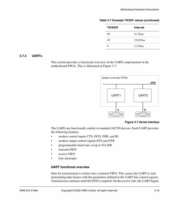
3.7.3 UARTs
This section provides a functional overview of the UARTs implemented in the motherboard FPGA. This is illustrated in Figure 3-7.
Figure 3-7 Serial interface
The UARTs are functionally similar to standard 16C550 devices. Each UART provides the following features:
• modem control inputs CTS, DCD, DSR, and RI
• modem output control signals RTS and DTR
• programmable baud rates of up to 921,600
• transmit FIFO
• receive FIFO
• four interrupts.
UART functional overview
Data for transmission is written into a transmit FIFO. This causes the UART to start transmitting data frames with the parameters defined in the UART line control register. Transmission continues until the FIFO is emptied. On the receive side, the UART begins
99 31.25ms
49 15.625ms
9 3.125ms
Table 3-7 Example TICDIV values (continued)
TICKDIV Interval
UART1 UART2
BA
APB
System controller FPGA
ARM DUI 0190A Copyright © 2002 ARM Limited. All rights reserved. 3-19

Motherboard Hardware Description
sampling after it receives a start bit (LOW level input). When a complete word has been received, it is stored in the receive FIFO together with any error bits associated with that word. See the EABBC Technical Reference Manual for details of the read FIFO bits.
The FIFOs can be disabled. In this case, the UART provides a 1-byte holding register for each of the transmit and receive channels. The overrun bit in the UART_RSR register is set and an interrupt is generated if a word is received before the previous one was read. As a feature of the UART, the FIFOs are not physically disabled but are bypassed. This means that if an overrun error occurs, the excess data is still stored in the FIFO and must be read out to clear the FIFO.
The baud rate of the UART is set by programming the UART_LCRM and UART_LCRL bit rate divisor registers.
For more information about the function and programming of the UARTs, refer to the EABBC Technical Reference Manual.
3.7.4 GPIO
The system controller FPGA incorporates two 8-bit General Purpose Input/Output (GPIO) ports. These connect to pins on the EXPB connector and then to the FPGAs on the BTLM. You can configure each of the 16 individual bit-ports as inputs or outputs. You can also configure any one bit from each GPIO port to trigger interrupt source on a rising or falling edge, or on a HIGH or LOW level.
The GPIO pins are assigned to the GPIO[15:0] signals that connect between the motherboard FPGA and FPGA2 on the BTLM. Figure 3-8 on page 3-21 shows the block diagram for the GPIO.
3-20 Copyright © 2002 ARM Limited. All rights reserved. ARM DUI 0190A

Motherboard Hardware Description
Figure 3-8 GPIO block diagram
EBCFPGA2
Port A Port B
Systemcontroller
FPGA
GPIO[7:0]
GPIO[15:8]
Motherboard
BTLM
ARM DUI 0190A Copyright © 2002 ARM Limited. All rights reserved. 3-21

Motherboard Hardware Description
GPIO direction
Each GPIO port has a data register and an associated data direction register. Each bit in the data direction register defines the corresponding bit in the data register as follows:
0 Bit is an input.
1 Bit is an output.
Figure 3-9 shows the function of the data direction register for one bit.
Figure 3-9 GPIO data direction register
GPIO writes
The GPIOs enable you to write to individual bits by using the address of the data register as a mask. It allows this by providing 255 read/write locations for each data register and using A[9:2] to mask data bits D[7:0]. This address-to-data bit alignment is used because each register location is aligned on a 32-bit boundary meaning that A[1:0] are always 0.
Data masking for writes functions as follows:
• Address bit = 0. The corresponding data bit written to the data register is masked, leaving the bit already in the data register unchanged.
• Address bit =1. The corresponding data bit is written into the data register.
GPIO masking for writes is illustrated in Figure 3-10 on page 3-23. This example shows what happens when you write the value 0xFF to the data register at offset address 0x2A8 (A[1:0]) are ignored). The data register already contains 0xCC from a previous access.
Data directionregister
Data register
GPIO pin
3-22 Copyright © 2002 ARM Limited. All rights reserved. ARM DUI 0190A

Motherboard Hardware Description
After the write, data bits 7, 5, 3, and 1 (that correspond with an address bits that are at 1) are changed in the data register. Data bits 6, 4, 2, and 0 are unchanged from the previous access, because address bits 8, 6, 4, and 2 are all at 0.
Figure 3-10 GPIO bit masking for a write
GPIO reads
The GPIOs also enable you to read individual bits by using address masking. In the case of reads, you read from one of the 255 read/write locations for each data register, using A[9:2] to mask data bits D[7:0]. This address-to-data bit alignment is used because each register location is aligned a 32 bit boundary meaning that A[1:0] are always 0.
Data masking for reads functions as follows:
• Address bit = 0. The corresponding data bit in the data register is masked, and a 0 is returned.
• Address bit =1. The corresponding data bit read from the data register.
0
7
1 0
4
1 1
16 5 3 2
1 0 0
0
0
9
0 0
6
1 0
38 7 5 4
1 1 1
2
1
7
1 1
4
1 1
16 5 3 2
1 1 1
0
0
7
1 0
4
1 1
16 5 3 2
1 1 1
0
1 0
0 0
Data registerbefore write
Data registeroffset addressused for write
Data written todata register
Result in dataregister afterwrite
ARM DUI 0190A Copyright © 2002 ARM Limited. All rights reserved. 3-23

Motherboard Hardware Description
GPIO data masking for reads is illustrated in Figure 3-11. This example shows what happens when you read from the data register at offset address 0x330 (A[1:0]) are ignored). GPIO pins 5, 4, 2, and 0 are ignored and 0s are returned.
Figure 3-11 GPIO bit masking for a read
0
7
0 0
4
1 0
16 5 3 2
1 1 1
0
0
9
1 0
6
1 1
38 7 4
1 0 0
2
0
7
0 0
4
1 0
16 5 3 2
1 0 0
0
1 0
0 0
GPIO pins
Data registeroffset addressused for read
Data read fromoffset address
5
3-24 Copyright © 2002 ARM Limited. All rights reserved. ARM DUI 0190A

Chapter 4 BTLM Hardware Description
This chapter describes BTLM hardware and contains the following sections:
• BTLM FPGAs on page 4-2
• JTAG support on page 4-7
• System bus interface on page 4-11
• BTLM clock control on page 4-12
• Reset control on page 4-14
• BTLM LEDs and switches on page 4-15
• Audio CODEC interface on page 4-16
• Diagnostic connections on page 4-17
• CIF connector on page 4-18.
ARM DUI 0190A Copyright © 2002 ARM Limited. All rights reserved. 4-1

BTLM Hardware Description
4.1 BTLM FPGAs
The BTLM is fitted with two Altera Apex 20K1000E FPGAs. These implement the functions of the EBC and are described in the following sections:
• FPGA functional description
• FPGA configuration on page 4-3.
4.1.1 FPGA functional description
Figure 4-1 shows the functional architecture of the FPGAs.
Figure 4-1 FPGA functional block diagram
FPGA1 incorporates the following functions:
• AHB master/slave interface
• voice encoder/decoder
• Link InterFace (LIF)
• DMA controller
• CIPher (CIP) block
• transmitter and receiver blocks
• controller block.
FPGA2 contains the multichannel PCM.
System bus(AHB)
FPGA1 FPGA2
AHBmaster
AHBslave
Linkinterface
(LIF)
Rx
Tx
Control
Voice
Cipherblock(CIP)
Radiomodule
Radiointerface
(RIF)
CIF
Lydi
a
CODECMultichannel
PCMInterface
DMA
4-2 Copyright © 2002 ARM Limited. All rights reserved. ARM DUI 0190A

BTLM Hardware Description
4.1.2 FPGA configuration
In normal operation, every time the BTLM is powered on, the FPGAs are reprogrammed using configuration data stored in flash memory as shown Figure 4-2.
Figure 4-2 FPGA configuration architecture
Figure 4-2 shows the architecture of the FPGA configuration system on the BTLM. The Multi-ICE and ByteBlasterMV/Masterblaster connectors are provided to allow you to download new FPGA images.
FPGA configuration is managed by the configuration PLD. This supplies the DCLK signal to provide timing for the process.
FPGA[21:0]
FnOE
FnWE
FD[7:0]
DCLK
nCONFIG
CONF_DONE
nSTATUSFPGA1
ConfigPLD
Configflash
FPGA2
Byt
eBla
ster
MV
Mul
ti-IC
E
ARM DUI 0190A Copyright © 2002 ARM Limited. All rights reserved. 4-3

BTLM Hardware Description
Note
There are two FPGA configurations, EBCP1v02 and EBCP1v04 (that is, EBCP 1.04). The EBCP1v04 configuration has the newer PL011 UART circuit with automatic hardware flow control.
The BTLM has three FPGA configuration modes. These are selected by setting S2[4] and setting the CONFIG link, as shown in Table 4-1.
Byte streamer mode
This is the normal mode and is selected by setting S2[4] to OFF and ensuring that the CONFIG link (J3) is OUT. In this mode, the FPGAs are configured from images stored in flash.
Flash programming mode
Use flash programmer mode to download, for example, a new configuration release into the flash memory. This new data is used to configure the FPGAs the next time the BLTM is powered on. Select flash programmer mode by setting S2[4] to ON and ensuring that the CONFIG link is OUT.
PLD programming mode
Use this mode to access to the JTAG port of the PLD to reprogram the configuration PLD, if required (see Reprogramming the PLD on page 4-6). Select this mode by setting S2[4] to OFF and fitting the CONFIG link. The CONFIG LED is lit when this mode is selected and the routing of the JTAG signals is changed (see JTAG signal routing in PLD programming mode on page 4-8).
Table 4-1 FPGA configuration modes
S2[4] CONFIG Mode selected
OFF OUT Byte streamer mode (user mode)
ON OUT Flash programming mode
OFF IN PLD programming mode/ByteBlasterMV mode
ON IN Nonvalid
4-4 Copyright © 2002 ARM Limited. All rights reserved. ARM DUI 0190A

BTLM Hardware Description
ByteblasterMV/Masterblaster mode
Use this mode to download volatile FPGA images using the Altera download tools (refer to Altera documentation). Select this mode by setting S2[4] to OFF and fitting the CONFIG link. The CONFIG LED is lit when this mode is selected.
4.1.3 Downloading FPGA configurations into FLASH
To reprogram the FPGA configuration flash, use the progcards utility. You can also use progcards to verify the flash image against a binary file.
Note This requires Progcards 2.00 or later.
To load new FPGA configurations into the flash:
1. Put the BTLM in flash program mode by setting S2[4] to CLOSED and removing the CONFIG link J3.
2. Configure the Multi-ICE server using a configuration file. For example: \BTLM_flash_program.cfg.
Note
The BTLM requires the JTAG TCK signal to operate at 1MHz maximum for flash programming. Load Multi-ICE with the configuration file. This sets TCK to 1MHz.
3. Run the progcards utility. All .brd files present in the current directory that match the TAP configuration are offered as options.
4. Set S2[4] to OPEN.
5. Power cycle the BTLM.
ARM DUI 0190A Copyright © 2002 ARM Limited. All rights reserved. 4-5

BTLM Hardware Description
4.1.4 Reprogramming the PLD
The BTLM is supplied with the PLD already programmed. These instructions are provided in case of accidental erasure or for upgrade.
Caution Only reprogram this device if the original design has been accidently erased or if you are updating the design. Only use images supplied by ARM Limited.
Program the PLD as follows:
1. Put the BTLM into PLD programming mode by setting S2[4] to OPEN, fitting the CONFIG link (J3), and powering up.
2. Start the Multi-ICE server and load the configuration file for your BTLM. For example: ..\BTLM_pld_program.cfg
3. Start a command prompt in the directory containing the .brd files.
4. Run the progcards utility by typing: progcards <ret>
5. Choose the required PLD image. If there is only one suitable match for your hardware, programming starts immediately with no menu being displayed.
4-6 Copyright © 2002 ARM Limited. All rights reserved. ARM DUI 0190A

BTLM Hardware Description
4.2 JTAG support
The BTLM provides support for reprogramming the FPGAs and PLD using JTAG. The Multi-ICE and Altera tool connectors provide access to the FPGA and PLD TAP controllers. The JTAG hardware is connected to the top board in the stack and the JTAG signals TMS, TCK, and TDI are routed directly down to the motherboard. From there, the TDO signal routed up from the motherboard through all devices on modules in the stack.
Note The motherboard provides separate logic module (EXPA/EXPB) and a core module (HDRA/HDRB) stacking positions. The JTAG signals in these two positions are completely isolated. Configure the BTLM using the JTAG connectors on the BTLM or logic module at the top of the EXPA/EXPB stack. To download and debug ARM code, use the JTAG connector on the core module.
4.2.1 JTAG signal routing in user mode
The routing of the JTAG signals depends on whether the BTLM is in configuration mode or user mode. The CONFIG link and S2[4] allow you to select between the JTAG modes (see FPGA configuration on page 4-3).
Figure 4-3 on page 4-8 shows the JTAG data routing for a logic module, BTLM, and motherboard in user mode. The TDI-TDO data path is routed first down to the motherboard and then up through the devices on each module in the stack.
The JTAG routing switches on the BTLM are controlled by the signal nMBDET from the motherboard. When the BTLM is mounted on the motherboard, nMBDET is pulled LOW and the JTAG path is correctly routed round the system.
ARM DUI 0190A Copyright © 2002 ARM Limited. All rights reserved. 4-7

BTLM Hardware Description
Figure 4-3 JTAG data path (byte streamer mode)
The JTAG port does not operate if the BTLM is stacked without a motherboard. This is because nMBDET is pulled HIGH, isolating the BTLM JTAG from other modules.
4.2.2 JTAG signal routing in PLD programming mode
When the BTLM is in PLD programing mode (see PLD programming mode on page 4-4) the JTAG signals are routed through the PLD and then the FPGAs. This is shown in Figure 4-4.
Figure 4-4 JTAG routing in PLD programming mode
Motherboard
FPGA
Mul
ti-IC
E
TDI TDI
nM
BD
ET
TDO
ARM Logic module
BTLMFPGAs
TDI
TDI
TDO
EXPB
EXPB
BTLM
EXPB
EXPB
TDI TDOFPGA1 FPGA2PLD
4-8 Copyright © 2002 ARM Limited. All rights reserved. ARM DUI 0190A

BTLM Hardware Description
4.2.3 JTAG signal descriptions
Table 4-2 shows the JTAG signals.
Table 4-2 JTAG and related signals
Signal Description Function
TDI Test Data In(from JTAG tool)
This signal is routed down the stack of modules to the motherboard and then up through any connected JTAG device on each module in the stack and returned to the Multi-ICE connector as TDO.
TDO Test Data Out (to JTAG tool)
This signal is the return path of the data input signal TDI. The BTLM connects to the TDO signal from the module beneath using the TDO_BELOW pin on the EXPB socket. The signal from this pin is routed through TAP controllers in devices on the BTLM as TDI and is then routed to the next module up the stack on the TDO pin of the EXPB plug. The length of track driven by the last component in the chain is kept as short as possible.
TCK Test Clock
(from JTAG tool)
This signal synchronizes all JTAG transactions. TCK connects to all JTAG components in the TDI-TDO chain. It makes use of series termination resistors on stubs to reduce reflections and maintain good signal integrity. TCK flows down the stack of modules and connects to each JTAG component, but if there is a device in the scan chain that synchronizes TCK to some other clock, then all down-stream devices are connected to the RTCK signal on that component (see RTCK below).
TMS Test Mode Select (from JTAG tool)
This signal controls transitions in the tap controller state machine. TMS connects to all JTAG components in the scan chain as the signal flows down the module stack.
RTCK ReturnTCK (to JTAG tool)
Some devices sample TCK (for example, a synthesizable core with only one clock), and this delays the time at which a component actually captures data. RTCK is used to return the sampled clock to the JTAG equipment, so that the TCK is not advanced until the synchronizing device has captured the data. In adaptive clocking mode, Multi-ICE must detect an edge on RTCK before changing TCK. In a multiple-device JTAG chain, the RTCK output from a component connects to the TCK input of the down-stream device. The RTCK signal on the module connectors HDRB/EXPB returns TCK to the JTAG equipment. If there are no synchronizing components in the TDI-TDO chain then, it is not necessary to use the RTCK signal and it is connected to ground on the motherboard.
ARM DUI 0190A Copyright © 2002 ARM Limited. All rights reserved. 4-9

BTLM Hardware Description
nRTCKEN Return TCK enable(from module to motherboard)
This active LOW signal is driven by any module that requires RTCK to be routed back to the JTAG equipment. If nRTCKEN is HIGH the motherboard drives RTCK LOW. If nRTCKEN is LOW, the motherboard drives the TCK signal back up the stack to the JTAG equipment. The BTLM drives this signal LOW when it is not in configuration mode. This signal is left unconnected by modules that do not require adaptive clocking.
nCFGEN Configuration enable(from jumper on module at the top of the stack)
This active LOW signal is used to put the boards into configuration mode. In configuration mode all FPGAs and PLDs are connected to the TDI-TDO chain so that they can be configured by the JTAG equipment.
FPGA_DONE All FPGAs are configured
This open-collector signal indicates when all FPGAs in the system have configured. This signal is not part of the JTAG scheme, but is relevant to how the boards are reset and, therefore, has an effect on nSRST. The signal is routed between all FPGAs in the system through a pin on the HDRB/EXPB connectors. The master reset controller on the motherboard senses this line and holds all the boards in reset (by driving nSRST LOW) until all the FPGAs are configured. It is essential that a pull-up is added to the FPGA input/output pad during synthesis.
Table 4-2 JTAG and related signals (continued)
Signal Description Function
4-10 Copyright © 2002 ARM Limited. All rights reserved. ARM DUI 0190A

BTLM Hardware Description
4.3 System bus interface
The BTLM communicates with the motherboard and core module over the AMBA AHB. For more information about the AHB, see System bus on page 3-3.
The BTLM provides a conventional master and slave interface. Transfers are supported by a DMA controller.
ARM DUI 0190A Copyright © 2002 ARM Limited. All rights reserved. 4-11

BTLM Hardware Description
4.4 BTLM clock control
Figure 4-5 shows the distribution of the clock signals on the BTLM.
Figure 4-5 Clock architecture
Both FPGAs on the BTLM receive the same clock signals and these are applied to the CLK and FAST pins of the devices. The solid state switch (U2) is used to select whether the BTLM is clocked from the motherboard or form the Lydia board. This switch is controlled by the mechanical switch S2[3].
Table 4-3 on page 4-13 provides a summary of the clock signals on the BTLM and the FPGA pins to which they are applied (where x=don’t care).
�����
�����������
���� �����
������������ ��
� !��"����������� ��
���������
��������
���������
��
��
�� �
����
��
�� �
�����
��
�����
��
�����
����
������
��#�
��#
��#$
��#%
��&�
��&
��#�
��#
��#$
��#%
��&�
��&
'
4-12 Copyright © 2002 ARM Limited. All rights reserved. ARM DUI 0190A

BTLM Hardware Description
Table 4-3 BTLM clock signals
FPGA pin name SW2[3] Clock name Clock source
CLK1 OPEN EBCLK Clock from motherboard FPGA.
CLOSED CLK Clock from Lydia board.
CLK2 OPEN EBHCLK Clock from motherboard.
CLOSED SYSCLK Clock from Lydia board.
CLK3 x RF_SYS_CLK From radio module.
CLK4 x PCMCLK From Lydia board.
FAST1 x RF_TX_CLK From the radio module. This signal is also routed to the Lydia board connector but this can be isolated by removing the zero ohm resistor R134.
FAST2 x RF_LPO_CLK From the radio module. This signal is also routed to the Lydia board connected but this can be isolated by removing the zero ohm resistor R135.
RF_LPO_CLK is also routed to the motherboard FPGA using the F[22]/GPIO[22] signal path.
FAST3 x Not used -
FAST4 x Not used -
ARM DUI 0190A Copyright © 2002 ARM Limited. All rights reserved. 4-13

BTLM Hardware Description
4.5 Reset control
The BTLM receives reset signals from the motherboard using the EXPB connector and from Mult-ICE. This is shown on Figure 4-6.
Figure 4-6 Reset architecture
4.5.1 JTAG test reset
The JTAG test reset signal, nTRST, is an active LOW open-collector signal. It is connected to the nTRST input on both FPGAs. The sources of the nTRST signal are:
• Multi-ICE connector
• motherboard or core module on the EXPB connectors.
Note On the Integrator/BTAP, the expansion connector (EXPB) version of nTRST is completely isolated from the core module (HDRB) version of nTRST.
4.5.2 Motherboard reset
The motherboard reset signal, nSYSRST, is driven by the motherboard system controller, and is routed to an FPGA input/output pin on both FPGAs on the BTLM (see the Integrator/AP User Guide for further information).
EX
PB
FPGAs
Mul
ti-IC
E
nTRST
nSRST
nSYSRST
4-14 Copyright © 2002 ARM Limited. All rights reserved. ARM DUI 0190A

BTLM Hardware Description
4.6 BTLM LEDs and switches
This section describes the EBC status LEDs and DIP switches on the BTLM.
4.6.1 EBC status LEDs
There are 16 LEDs. The first eight of these provide status indications for the radio module. The second eight indicate the FPGA version. Table 1-5 on page 1-16 shows the assignment of the LEDs.
4.6.2 BTLM switches
The BTLM provides a 4-way DIP switch that is used to select the system clock source and to select the FPGA programming mode. The switches are assigned as shown in Table 4-4.
4.6.3 Push button
The push button is a general-purpose switch that provides an active HIGH input to an input/output pin on the FPGA.
Table 4-4 BTLM DIP switch assignment
Switch element
Function Setting Description
1 CIF/Radio module select OFF BDP uses the radio module to communicate with other Bluetooth devices over a radio link.
ON The BDP uses CIF connector to communicate with other Bluetooth devices instead of a radio link. However, the radio module must still be present because it provides timing signals for the CIF connection.
2 PCM mode OFF PCM interfaces is routed to the CODEC.
ON PCM interface is routed to the Lydia connector. See BTLM Codec Add-on Board (EN/LZT 108 5570/30) for more information about PCM operating modes.
3 Clock source select OFF The BTLM is clocked from the motherboard.
ON The BTLM is clocked from Lydia.
4 FPGA configuration mode OFF Byte streamer mode.
ON Flash program mode.
ARM DUI 0190A Copyright © 2002 ARM Limited. All rights reserved. 4-15

BTLM Hardware Description
4.7 Audio CODEC interface
The BTLM provides an audio interface to which you can connect, for example, a telephone handset. The interface uses an MSM7540 APDCM CODEC device to provide translation between analog voice input/output side and pulse code modulated digital input/output side.
Figure 4-7 shows the CODEC interface of the BTLM. The connector makes 5V, 12V, and –12V power rails available for an optional external amplifier. These power rails are supplied by the motherboard (see Connecting power on page 2-5).
Figure 4-7 CODEC interface
A connecting lead and telephone handset are supplied. The handset connections are shown in Table 4-5.
�������
�(���
�����
�������
�)('&
�)*+
�+�
,-
�-
.�-
/$%
Table 4-5 Telephone handset wiring
Signal Wire color Jack socket
GND Black Body
A_IN Blue Tip
A_OUT Yellow Ring
4-16 Copyright © 2002 ARM Limited. All rights reserved. ARM DUI 0190A

BTLM Hardware Description
4.8 Diagnostic connections
The BTLM provides four 38-way Mictor logic analyzer connectors. These are reserved for production purposes.
ARM DUI 0190A Copyright © 2002 ARM Limited. All rights reserved. 4-17

BTLM Hardware Description
4.9 CIF connector
You can use the CIF connector to connect two BTLMs together using a 20-way ribbon cable in place of the radio connection. However, the radio module must still be present to provide timing for communications that use the CIF link. To enable CIF link communications, set S2[1] to ON on both BTLMs.
Figure 4-8 shows the pinout of the CIF connector.
Figure 4-8 CIF connector pinout
The 20-way ribbon cable must provide crossover connections for the CIF_RX_DATA and CIF_TX_DATA as shown in Figure 4-9. Although not shown, all other signals must be connected straight through.
Figure 4-9 CIF crossover connection
GND ReservedGND Reserved
ReservedReservedReservedReservedReservedReservedReserved
GND CIF_RX_DATAGND CIF_TX_DATA
GNDGNDGNDGNDGND
1
19
2
20
1
1920
2
6 6
88
21
1920
4-18 Copyright © 2002 ARM Limited. All rights reserved. ARM DUI 0190A

Chapter 5 Programmer’s Reference
This chapter describes the BDP memory map and registers. It contains the following sections:
• System memory map description on page 5-2
• Bluetooth UART on page 5-7
• Bluetooth GPIO on page 5-8
• Bluetooth interrupt controller on page 5-9
• Bluetooth system controller on page 5-12
• Motherboard peripherals on page 5-13.
ARM DUI 0190A Copyright © 2002 ARM Limited. All rights reserved. 5-1

Programmer’s Reference
5.1 System memory map description
The memory map for the BDP combines the features of the EABBC memory map with the memory map of the Integrator development system. The map includes resources located on the motherboard and the attached core module and BTLM. The memory map is shown in Figure 5-1.
Figure 5-1 Top level system memory map
Reserved
Reserved
Reserved
Reserved
Reserved
Bluetooth peripherals
Integrator peripherals
Core modulememory and registers0x00000000
0x10000000
0x20000000
0x30000000
0x40000000
0x50000000
0x60000000
0x70000000
0x80000000
0x90000000
0xC0000000
0xD0000000
0xE0000000Logic module 1
(optional)
BTLM alias
BTLM
External bus interface
Core module 0 (CM7TDMI)
5-2 Copyright © 2002 ARM Limited. All rights reserved. ARM DUI 0190A
Programmer’s Reference
Table 5-1 shows the memory map of the BDP.
Note The addresses shown for core modules and logic modules (including the BTLM) in Figure 5-1 on page 5-2 and Table 5-1 rely on the core module(s) being plugged into to the HDRA/HDRB connectors and logic module(s) being plugged into the EXPA/EXPB connectors.
Table 5-1 System memory map
Address range Size Device Comment
0xE0000000 to 0xFFFFFFFF 256MB Reserved Bus error if accessed.
0xD0000000 to 0xDFFFFFFF 256MB Logic module 1 If fitted, must be mounted on top of the BTLM and must decode its assigned address space and generate bus responses.
0xC0000000 to 0xCFFFFFFF 256MB Reserved for BTLM Must be BTLM mounted directly on motherboard.
0xA0000000 to 0xBFFFFFFF 768MB Reserved Bus error if accessed.
0x80000000 to 0x9FFFFFFF 256GB Core module alias region Contains aliases of the core module SDRAM.
0x70000000 to 0x7FFFFFFF 256MB Reserved Bus error if accessed.
0x60000000 to 0x6FFFFFFF 256MB Static memory interface Implemented in place of Bluetooth static memory controller.
0x50000000 to 0x5FFFFFFF 256MB Reserved Bus error if accessed.
0x40000000 to 0x4FFFFFFF 256MB Bluetooth peripherals region Contains the standard Bluetooth peripherals.
0x30000000 to 0x3FFFFFFF 256MB BTLM alias BTLM.
0x20000000 to 0x2FFFFFFF 256MB Reserved For Bluetooth static memory controller.
0x10000000 to 0x1FFFFFFF 256MB Integrator peripherals Contains Integrator-specific peripherals, such as the alphanumeric display register.
0x00000000 to 0x0FFFFFFF 256MB Core module memory First 256KB selects bootROM unless REMAP bit is set in core module registers.
ARM DUI 0190A Copyright © 2002 ARM Limited. All rights reserved. 5-3

Programmer’s Reference
5.1.1 Logic module region
The logic module region contains two valid 256MB areas assigned to the BTLM and to an optional logic module. The lowest 256MB area contains an alias of the EBC registers that appear at 0x30000000. The memory map of this region is shown in Table 5-2.
The BTLM contains the EBC (see the EABBC Technical Reference Manual).
5.1.2 Core module region
This region contains the SDRAM on any core modules in the system. All system bus masters can access the SDRAM on any core module at the addresses shown in Table 5-3. The location of each core module in this region is determined by its position on the stack on the HDRA/HDRB connectors. Accesses to regions where no core module is fitted generate bus errors.
Table 5-2 Logic module address decoding
Address range Size Description
0xF0000000 to 0xFFFFFFFF 256MB Reserved
0xE0000000 to 0xEFFFFFFF 256MB Reserved
0xD0000000 to 0xDFFFFFFF 256MB Logic module 1 (optional)
0xC0000000 to 0xCFFFFFFF 256MB BTLM
Table 5-3 Aliased core module memory
Address range Size Description Comment
0xB0000000 to 0xBFFFFFFF 256MB Core module 3 alias -
0xA0000000 to 0xAFFFFFFF 256MB Core module 2 alias -
0x90000000 to 0x9FFFFFFF 256MB Core module 1 alias -
0x80000000 to 0x8FFFFFFF 256MB Core module 0 alias Always the CM7TDMI
5-4 Copyright © 2002 ARM Limited. All rights reserved. ARM DUI 0190A

Programmer’s Reference
5.1.3 Static memory interface region
The SMI region provides access to four areas of memory. These contain the bootROM, flash and SRAM, and an expansion module connector EXPM. This cannot be used when the BTLM is fitted. Table 5-4 shows the memory map of the SMI space.
Accesses to the bootROM or flash on the motherboard, and SSRAM on the core module, are selected by the REMAP bit (bit 2 of the CM_CTL register at 0x1000000C). See the Integrator/CM7TDMI Core Module user guide for more information.
5.1.4 Bluetooth peripherals region
This region contains the Bluetooth peripherals. These are:
• Bluetooth UART on page 5-7
• Bluetooth GPIO on page 5-8
• Bluetooth interrupt controller on page 5-9
• Bluetooth system controller on page 5-12.
Table 5-5 shows the base addresses for the registers for each device.
Table 5-4 SMI chip selects
Base address Bus width Description
0x6C000000 8, 16, or 32-bits Chip select 3 Unused
0x68000000 32-bits Chip select 2 SRAM
0x64000000 32-bits Chip select 1 Flash
0x60000000 8-bits Chip select 0 bootROM
Table 5-5 Bluetooth registers
Base address Size Description
0x45000000 to 0x4FFFFFFF - Not used
0x44000000 16MB Bluetooth UART2, general purpose
0x43000000 16MB Bluetooth UART1, HCI
0x42000000 16MB Bluetooth GPIO
0x41000000 16MB Bluetooth interrupt controller
0x40000000 16MB Bluetooth system controller
ARM DUI 0190A Copyright © 2002 ARM Limited. All rights reserved. 5-5

Programmer’s Reference
5.1.5 Integrator peripheral region
This region contains the Integrator peripherals. Table 5-5 on page 5-5 shows the base addresses for the registers in this region (see Motherboard peripherals on page 5-13).
5.1.6 Core module region
The region from 0x00000000 to 0x10FFFFFF contains the SDRAM, SSRAM, and control registers on the core module. These locations are only decoded on the core module and are only accessible by the processor on the same core module. Each core module added to the system maps its own SDRAM, SSRAM, and control registers into this address range. However, all other locations, from 0x11000000 upwards are shared and can be accessed by any system bus master.
For details of this region, see the Integrator/CM7TDMI User Guide.
Table 5-6 Peripheral registers
Base address Size Description
0x1B000000 to 0x1FFFFFFF - Not used
0x1A000000 16MB LED display and boot switch
0x13000000 to 0x19FFFFFF - Not used
0x12000000 16MB Static memory interface registers
0x11000000 16MB System control registers
0x10000000 16MB Core module registers
5-6 Copyright © 2002 ARM Limited. All rights reserved. ARM DUI 0190A

Programmer’s Reference
5.2 Bluetooth UART
This section describes the UARTs implemented in the system controller FPGA on the motherboard. The UART registers are shown in Table 5-7.
For descriptions of the Buetooth UART registers, refer to the EABBC Technical Reference Manual.
Note
There are two FPGA configurations, EBCP1v02 and EBCP1v04. The EBCP1v04 configuration has a newer PL011 UART circuit. See also the EABBC Software Integration Guide.
Table 5-7 UART register summary
UART1 UART2 Label Access Function
0x43000000 0x44000000 UARTDR Read Receive data
Write Transmit data
0x43000004 0x44000004 UARTRSR Read Receive status register
UARTECR Write Error clear register
0x43000018 0x44000018 UARTFR Read Flag register
0x43000020 0x44000020 UARTILPR Read/write IrDA low-power counter register
0x43000024 0x44000024 UARTBRD Read/write Baud rate divisor register
0x43000028 0x44000028 UARTLCR_H Read/write Line control register, high byte
0x4300002C 0x4400002C UARTCR Read/write Control register
0x43000030 0x44000030 UARTFLS Read/write Interrupt FIFO level select register
0x43000034 0x44000034 UARTIMSC Read/write Interrupt mask set/clear register
0x43000038 0x44000038 UARTRIS Read/write Raw interrupt status register
0x4300003C 0x4400003C UARTMIS Read Masked interrupt status register
0x43000040 0x44000040 UARTCR Write Interrupt clear register
ARM DUI 0190A Copyright © 2002 ARM Limited. All rights reserved. 5-7
Programmer’s Reference
5.3 Bluetooth GPIO
The Bluetooth GPIO registers are shown Table 5-8.
For a description of the Bluetooth GPIO registers, refer to the EABBC Technical Reference Manual.
Table 5-8 Bluetooth GPIO register summary
Address Type Label Name
0x42000000 - - Reserved
0x42000004 to 0x420003FC Read/write GPIO_PADR Port A data register
0x42000400 - - Reserved
0x42000404 to 0x420007FC Read/write GPIO_PBDR Port B data register
0x42000800 Read/write GPIO_PADDR Port A data direction register
0x42000804 Read/write GPIO_PBDDR Port B data direction register
0x42000808 Read/write GPIO_INTC1 GPIO Interrupt 1 control register
0x4200080C Read/write GPIO_INTC2 GPIO Interrupt 2 control register
0x42000840 to 0x42000888 - - Reserved
0x4200088C to 0x42000FFF - - Reserved
5-8 Copyright © 2002 ARM Limited. All rights reserved. ARM DUI 0190A

Programmer’s Reference
5.4 Bluetooth interrupt controller
The interrupt controller provides interrupt handling for the processor IRQ and FIQ inputs.
5.4.1 Interrupt control register memory map
The base address of the interrupt controller is not fixed and can be different for any particular system implementation. However, the offset of any particular register from the base address is fixed. Table 5-9 shows the register memory map.
Note
Two extra read/write registers are defined for both FIQ and IRQ to allow testing of the interrupt controller module using the AMBA test methodology. They must not be accessed during normal operation.
Table 5-9 Interrupt Controller register summary
Address Label Read function Write function
0x41000000 IRQ_STATUS IRQ status register -
0x41000004 IRQ_RAWSTAT IRQ raw status register -
0x41000008 IRQ_ENABLESET IRQ enable register IRQ enable set register
0x4100000C IRQ_ENABLECLR - IRQ enable clear register
0x41000010 IRQ_SOFT - IRQ soft interrupt register
0x41000014 to 0x410000FF - Reserved Reserved
0x41000100 FIQ_STATUS FIQ status register -
0x41000104 FIQ_RAWSTAT FIQ raw status register -
0x41000108 FIQ_ENABLESET FIQ enable register FIQ enable set register
0x4100010C FIQ_ENABLECLR - FIQ enable clear register
0x41000110 to 0x410001FF - Reserved Reserved
0x41000200 - Reserved for Test Reserved
0x41000210 to 0x41000FFF - Reserved Reserved
ARM DUI 0190A Copyright © 2002 ARM Limited. All rights reserved. 5-9

Programmer’s Reference
5.4.2 Register descriptions
The FIQ and IRQ interrupt controllers provide separate but functionally similar sets of registers to control interrupts. These are as follows:
• IRQ/FIQ status register
• IRQ/FIQ raw status
• IRQ/FIQ enable set register
• IRQ/FIQ enable clear register
• IRQ software interrupt register.
IRQ/FIQ status register
The IRQ and FIQ status registers contain a logical AND of the bits in the raw status register and the enable register. A bit set to 1 indicates that the associated interrupt is active and is able to generate an interrupt to the processor.
IRQ/FIQ raw status
The IRQ and FIQ raw status registers provide an indication of the signal level on the interrupt request pins of the interrupt controllers. A bit set to 1 indicates that the associated interrupt request is active.
IRQ/FIQ enable set register
The IRQ and FIQ enable set register locations are used to set bits in the interrupt enable registers as follows:
• write a 1 to SET the associated bit in the register to 1
• write a 0 to leave the associated bit in the register unchanged.
IRQ/FIQ enable clear register
The IRQ and FIQ enable clear locations are used to clear bits in the interrupt enable registers as follows:
• write a 1 to CLEAR the associated bit in the register to 0
• write a 0 to leave the associated bit in the register unchanged.
IRQ software interrupt register
The IRQ software interrupt register is used to generate a a programmed interrupt:
• write a 1 to bit 1 to generate a programmed interrupt
• write a 0 to bit 1 to clear programmed interrupt.
5-10 Copyright © 2002 ARM Limited. All rights reserved. ARM DUI 0190A

Programmer’s Reference
The value of this register can be read from bit 1 of the status register. Bit 0 of this register is not used.
5.4.3 Interrupt register bit assignments
The FIQ interrupt controller registers are 2 bits wide. The interrupts are assigned to bits 0 and 1. Bit 0 is used for the EBC interrupt and bit 1 is the software interrupt bit.
The IRQ registers are 32 bits wide. Bits 0 and 1 in the IRQ sources are connected to the FIQ sources so that these sources are available in identical bit positions. Table 5-10 shows the bit assignments of the interrupt sources to the IRQ registers.
Table 5-10 BDP IRQ Interrupt sources
Bit Label Description
0 EBC_INT From the EBC
1 SOFT_INT For Licensee to use (to match FIQ)
2 PROG_INT Software interrupt
3 - Reserved
4 - Reserved
5 PFAIL_INT Power fail indication
6 TIMER1_INT Timer 1 indicating it has reached zero
7 TIMER2_INT Timer 2 indicating it has reached zero
8 TIMER3_INT Timer 3 indicating it has reached zero
9 TICK_INT Watchdog timer reached first timeout
10 UART1_INT Combined UART 1 Interrupt
11 UART2_INT Combined UART 2 Interrupt
12 GPIO_INT1 GPIO interrupt 1
13 GPIO_INT2 GPIO interrupt 2
14 Reserved -
15 EXPINT1 Logic module interrupt from optional logic module
31:16 Reserved -
ARM DUI 0190A Copyright © 2002 ARM Limited. All rights reserved. 5-11

Programmer’s Reference
5.5 Bluetooth system controller
The Bluetooth system controller registers are incorporated into the FPGAs on the BTLM. These implement the standard control functionality of the EABBC. For more information, see the EABBC Technical Reference Manual.
5-12 Copyright © 2002 ARM Limited. All rights reserved. ARM DUI 0190A

Programmer’s Reference
5.6 Motherboard peripherals
This section describes the Integrator peripherals. These are sets of registers that are used to:
• LED control and boot switch registers
• Motherboard status and control registers on page 5-17
• SMI control registers on page 5-22.
5.6.1 LED control and boot switch registers
A set of registers is used to control the alphanumeric display and LEDs, and to read the 4-way DIP switch. These are:
• Alphanumeric character register
• Motherboard LED control register on page 5-15
• Motherboard boot switch register on page 5-16.
Table 5-11 shows the addresses of these registers.
Alphanumeric character register
Use the AP_ALPHA register to write characters to the alphanumeric display. The system controller FPGA manages the transfer of character data into a shift register within the alphanumeric display. This means you must allow each transfer to complete before writing new characters to the display. To ensure this:
1. Check that the display status is IDLE (bit 0 = 0) in the AP_ALPHA register.
2. Write two characters to the AP_ALPHA register (bits 31:1).
Note The data in the AP_ALPHA register is shifted out to the alphanumeric display within the same bit-stream as the LED control bits in AP_LEDS register.
Table 5-11 LED control and switch registers
Address Name Type Size Function
0x1A000000 AP_ALPHA Read/write 32 Motherboard alphanumeric display characters register
0x1A000004 AP_LEDS Read/write 4 Motherboard LED control register
0x1A000008 AP_SWITCHES Read 4 Motherboard boot switch register
ARM DUI 0190A Copyright © 2002 ARM Limited. All rights reserved. 5-13
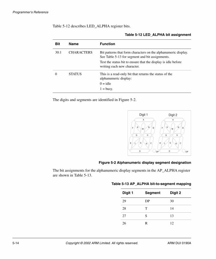
Programmer’s Reference
Table 5-12 describes LED_ALPHA register bits.
The digits and segments are identified in Figure 5-2.
Figure 5-2 Alphanumeric display segment designation
The bit assignments for the alphanumeric display segments in the AP_ALPHA register are shown in Table 5-13.
Table 5-12 LED_ALPHA bit assignment
Bit Name Function
30:1 CHARACTERS Bit patterns that form characters on the alphanumeric display. See Table 5-13 for segment and bit assignments.
Test the status bit to ensure that the display is idle before writing each new character.
0 STATUS This is a read-only bit that returns the status of the alphanumeric display:
0 = idle
1 = busy.
A
B
C
D
E
F
G H
KM
N
RST
DP
Digit 1A
B
C
D
E
F
G H
KM
N
RST
DP
Digit 2
Table 5-13 AP_ALPHA bit-to-segment mapping
Digit 1 Segment Digit 2
29 DP 30
28 T 14
27 S 13
26 R 12
5-14 Copyright © 2002 ARM Limited. All rights reserved. ARM DUI 0190A

Programmer’s Reference
Motherboard LED control register
The AP_LEDS register controls four of the LEDs on the motherboard. The LEDs are controlled by bit-ports provided by the alphanumeric display and accesses are managed by the FPGA. Application programs write appropriate values into the AP_LEDS register, and the FPGA carries out the necessary transfer to turn the LEDs ON or OFF.
You must allow each transfer the alphanumeric display to complete before writing new data to the display. To ensure this:
1. Check the display status is IDLE (bit 0 = 0) in the AP_ALPHA register.
2. Write a value to the AP_LEDS register.
Note The data from the AP_LEDS register is transferred as a serial bit-stream into the alphanumeric display at the same time as the character data in AP_ALPHA register.
The bit assignments for the AP_LEDS register are shown in Table 5-14 on page 5-16.
25 N 11
24 M 10
23 K 9
22 H 8
21 G 7
20 F 6
19 E 5
18 D 4
17 C 3
16 B 2
15 A 1
Table 5-13 AP_ALPHA bit-to-segment mapping (continued)
Digit 1 Segment Digit 2
ARM DUI 0190A Copyright © 2002 ARM Limited. All rights reserved. 5-15

Programmer’s Reference
Motherboard boot switch register
Use this register to read the 4-pole DIP switch SW1. The bit assignments for this register are shown in Table 5-15. A bit reads as 1 when the associated switch is ON and 0 when the switch is OFF.
Table 5-14 AP_LEDS register
Bit Type Function
3 Read/write LED3
0 = OFF
1 = ON.
2 Read/write LED2
0 = OFF
1 = ON.
1 Read/write LED1
0 = OFF
1 = ON.
0 Read/write LED0
0 = OFF
1 = ON.
Table 5-15 AP_SWITCH register
Bit Type Function
3 Read-only Switch pole 4 (S1-4)
2 Read-only Switch pole 3 (S1-3)
1 Read-only Switch pole 2 (S1-2)
0 Read-only Switch pole 1 (S1-1)
5-16 Copyright © 2002 ARM Limited. All rights reserved. ARM DUI 0190A

Programmer’s Reference
5.6.2 Motherboard status and control registers
The motherboard system controller FPGA contains registers that are used to configure operations of the motherboard. The registers in this section are:
• System controller identification register on page 5-18
• Motherboard oscillator divisor register on page 5-19
• Control register set/clear registers on page 5-20
• Decoder status register on page 5-21
• Motherboard lock register on page 5-21.
Table 5-16 shows the system controller registers.
Note These registers are usually controlled by firmware in the bootROM, so exercise care when accessing them.
All registers are accessed as 32-bit registers and do not support byte writes. Write operations must be word-wide. Spare bits that are not detailed or bits that are marked as reserved in the following sections must be preserved using read-modify-write operations.
Table 5-16 System controller status and control registers
Address Name TypeSize (bits)
Function
0x11000000 SC_ID Read 32 System controller identification
0x11000004 SC_OSC Read/write 8 Oscillator divisors
0x11000008 SC_CTRLS Read/write 8 Control register set
0x1100000C SC_CTRLC Read/write 8 Control register clear
0x11000010 SC_DEC Read 8 Decoder status
0x11000014 Reserved - - -
0x11000018 Reserved - - -
0x1100001C SC_LOCK Read/write 17 Lock register
ARM DUI 0190A Copyright © 2002 ARM Limited. All rights reserved. 5-17

Programmer’s Reference
System controller identification register
The system controller ID register (SC_ID) is a 32-bit read-only register that identifies the board manufacturer, board type, and revision.
Table 5-17 describes the system controller ID register bits.
Table 5-17 SC_ID register
Bits Name Type Function
31:24 MAN Read Manufacturer ID (0x41=ARM).
23:16 ARCH Read Architecture:0x00 = ASB little-endian0x01 = AHB little-endian.
15:12 FPGA Read System controller FPGA type:1 = XC40622 = XC4085.
11:4 BUILD Read Build value (ARM internal development only).
3:0 VER Read Version:
0 = Revision A
1 = Revision B.
5-18 Copyright © 2002 ARM Limited. All rights reserved. ARM DUI 0190A

Programmer’s Reference
Motherboard oscillator divisor register
The oscillator divisor register (SC_OSC) contains nine active bits that are used to set the frequency of the system bus clock clocks.
Note Before writing to the SC_OSC register, unlock it by writing the value 0x0000A05F to the SC_LOCK register. When you have finished writing to the SC_OSC register, lock it again by writing any value other than 0x0000A05F to the SC_LOCK register.
Table 5-18 describes the oscillator divisor register bits.
Table 5-18 SC_OSC register
Bits Name Type Function
8 Reserved - Reserved.
7:0 S_VDW Read/write These bits are used to set the frequency of the system bus clock signal SYSCLK. They control the value of the lower 8 VCO divider bits within the clock generator chip. The range of values for this bit-field is 4-192 (decimal) (giving 3-50 MHz in 0.25 MHz steps).
Values below 4 and above 192 are not permitted.
ARM DUI 0190A Copyright © 2002 ARM Limited. All rights reserved. 5-19

Programmer’s Reference
Control register set/clear registers
The system control register (SC_CTRL) is accessed using the SC_CTRLS and SC_CTRLC locations. The system control register is an 8-bit register that is used to control the UART modem lines, provide flash memory protection, and for software reset.
Set, read, and clear bits in the system controller register as follows:
• Set bits in the control register by writing to the SC_CTRLS location:
— write 1 to SET the associated bit in the control register
— write a 0 to leave the associated bit in the control register unchanged.
• Read the current state of the control register bits from the SC_CTRLS location
• Clear bits in the control register by writing to the SC_CTRLC location:
— write 1 to CLEAR the associated bit in the control register
— write 0 to leave the associated bit in the control register unchanged.
Table 5-19 describes the bits in the system control register.
Table 5-19 System control register
Bits Name Function
7:3 - Reserved
2 FLASHWP Flash write-protection:0 = protected (default)1 = unprotected.
1 FLASHVPP Flash Vpp enable:0 = disabled (default)1 = enabled.
0 - Reserved.
5-20 Copyright © 2002 ARM Limited. All rights reserved. ARM DUI 0190A

Programmer’s Reference
Decoder status register
The decoder status register (SC_DEC) is an 8-bit read-only register that provides information about any modules that are stacked on the EXP and HDR connectors. Table 5-20 describes the bits in the status decoder register.
Motherboard lock register
The lock register (SC_LOCK) is used to control access to the SC_OSC register, allowing it to be locked and unlocked. Use this mechanism to protect SC_OSC registers from being accidently overwritten with values that might render the system inoperable. Table 5-21 describes the lock register bits.
Table 5-20 SC_DEC register
Bits Name Function
7:4 EXP[3:0] Module present on EXP connectors, 1 bit for each module:
0000 = no modules fitted
0001 = module 0 fitted
0011 = module 1 and 0 fitted
0111 = module 2, 1, and 0 fitted
1111 = module 3, 2, 1, and 0 fitted.
3:0 HDR[3:0] Module present on HDR connectors 1 bit for each module:
0000 = no modules fitted
0001 = module 0 fitted
0011 = module 1 and 0 fitted
0111 = module 2, 1, and 0 fitted
1111 = module 3, 2, 1, and 0 fitted.
Table 5-21 SC_LOCK register
Bits Name Function
16 LCK Lock bit. Read this bit to determine if the SC_OSC register is locked:
0 = unlocked1 = locked.
15:0 LOCK Lock key. Write 0xA05F to unlock the SC_OSC register.
Write any other value to lock the SC_OSC register.
ARM DUI 0190A Copyright © 2002 ARM Limited. All rights reserved. 5-21
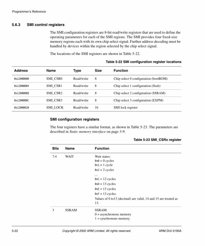
Programmer’s Reference
5.6.3 SMI control registers
The SMI configuration registers are 8-bit read/write registers that are used to define the operating parameters for each of the SMI regions. The SMI provides four fixed-size memory regions each with its own chip select signal. Further address decoding must be handled by devices within the region selected by the chip select signal.
The locations of the SMI registers are shown in Table 5-22.
SMI configuration registers
The four registers have a similar format, as shown in Table 5-23. The parameters are described in Static memory interface on page 3-9.
Table 5-22 SMI configuration register locations
Address Name Type Size Function
0x12000000 SMI_CSR0 Read/write 8 Chip select 0 configuration (bootROM)
0x12000004 SMI_CSR1 Read/write 8 Chip select 1 configuration (flash)
0x12000008 SMI_CSR2 Read/write 8 Chip select 2 configuration (SSRAM)
0x1200000C SMI_CSR3 Read/write 8 Chip select 3 configuration (EXPM)
0x12000020 SMI_LOCK Read/write 16 SMI lock register
Table 5-23 SMI_CSRx register
Bits Name Function
7:4 WAIT Wait states: 0x0 = 0 cycles 0x1 = 1 cycle
0x2 = 2 cycles
...0xC = 12 cycles
0xD = 13 cycles
0xE = 13 cycles
0xF = 13 cycles.
Values of 0 to13 (decimal) are valid, 14 and 15 are treated as 13.
3 SSRAM SSRAM:0 = asynchronous memory1 = synchronous memory.
5-22 Copyright © 2002 ARM Limited. All rights reserved. ARM DUI 0190A

Programmer’s Reference
The default values in the SMI_CSRx registers are shown in Table 5-24.
SMI lock register
The lock register (SMI_LOCK) is used to enable and disable accesses to the SMI registers. This protects the SMI_CSRx registers from accidental writes with values that could stop the system operating. Table 5-25 describes the lock register bits.
2 WREN Write enable:0 = writes disabled (default)1 = writes enabled.
1:0 MEMSIZE Memory size:
00 = 8 bit01 = 16 bit10 = 32 bit11 = reserved.
Table 5-23 SMI_CSRx register (continued)
Bits Name Function
Table 5-24 SMI_CSRx default values
RegisterDefault Value
WAIT SSRAM WREN MEMSIZE Device
SMI_CSR0 0x20 2 cycles Asynchronous Disabled 8 bit bootROM
SMI_CSR1 0x22 2 cycles Asynchronous Disabled 16 bit Flash
SMI_CSR2 0x0E 0 cycles Synchronous Enabled 32 SSRAM
SMI_CSR3 Undefined - - - - User defined
Table 5-25 SMI_LOCK register
Bits Name Function
16 LCK Lock bit. Read this bit to determine if the SMI_CSRx registers is locked:
0 = unlocked 1 = locked.
15:0 LOCK Lock key. Write 0xA05F to unlock the SMI_CSRx registers.
Write any other value to lock the SMI_CSRx register.
ARM DUI 0190A Copyright © 2002 ARM Limited. All rights reserved. 5-23

Programmer’s Reference
5-24 Copyright © 2002 ARM Limited. All rights reserved. ARM DUI 0190A

Appendix A Connector Pinouts
This appendix describes the BDP interface connectors and signal connections. It contains the following sections:
• Motherboard connectors HDRA and EXPA on page A-2
• Motherboard connector HDRB on page A-4
• Motherboard and BTLM connectors EXPB on page A-6
• Expansion connector EXPM on page A-9
• Serial interface connectors on page A-11
• Multi-ICE (JTAG) on page A-12
• Diagnostic connectors on page A-13.
ARM DUI 0190A Copyright © 2002 ARM Limited. All rights reserved. A-1

Connector Pinouts
A.1 Motherboard connectors HDRA and EXPA
Figure A-1 shows the pin numbering for the HDRA and EXPA plugs.
Figure A-1 Connector pin numbering
101
A2
GNDGND
D0D1
D2
GNDGND
D3
A5D4
D5
GNDGND
D6
A8D7
D8
GNDGND
D9
A11D10
D11
A14
GNDGND
D12D13
D14
GNDGND
D15
A17D16
D17
GNDGND
D18
A20D19
D20
GNDGND
D21
A23D22
D23
A0
A1
A3
A4
A6
A7
A9
A10
A12
A13
A15
A16
A18
A19
A21
A22
1
23456789
1011121314151617181920212223242526272829303132333435363738394041424344454647484950515253545556575859606162636465666768697071727374757677
78798081828384858687888990919293949596979899
100
A26
GNDGND
D24D25
D26
GNDGND
D27
A29D28
D29
GNDGND
D30
B0D31
C0
GNDGND
C1
B3C2
C3
B6
GNDGND
C4C5
C6
GNDGND
C7
B9C8
C9
GNDGND
C10
B12C11
C12
GNDGND
C13
B15C14
C15
A24
A25
A27
A28
A30
A31
B1
B2
B4
B5
B7
B8
B10
B11
B13
B14
B18
GNDGND
C16C17
C18
GNDGND
C19
B21C20
C21
GNDGND
C22
B24C23
C24
GNDGND
C25
B27C26
C27
B30
GNDGND
C28C29
C30
GNDGND
C31
3V33V3
12V
3V33V3
12V
3V33V3
12V
3V33V3
12V
3V33V3
12V
B16
B17
B19
B20
B22
B23
B25
B26
B28
B29
B31
5V
5V
5V
5V
5V
3V3
3V3
12V5V
3V35V 3V3
12V
102
114113112111110109108107106105104103
115
116
128127126125124123122121120119118117
129
130
142141140139138137136135134133132131
143
144
156155154153152151150149148147146145
157
158159160
161
173172171170169168167166165164163162
174
175176177
178
190189188187186185184183182181180179
191
192193194
195
200199198197196
Samtec TOLC series
Pin numbers for 200-way plug,viewed from above board
1
2
3
102
101
103
A-2 Copyright © 2002 ARM Limited. All rights reserved. ARM DUI 0190A

Connector Pinouts
The signals present on the pins labeled A[31:0], B[31:0], C[31:0], and D[31:0] are shown in Table A-1.
Table A-1 Bus bit assignment (for an AMBA AHB bus)
Pin label Signal Description
A[31:0] HADDR[3:0] System address bus
B[31:0] Not used -
C[31:16] Not used -
C15 HLOCKALL Locked transaction
C[14:13] HRESP[1:0] Slave response
C12 HREADY Slave ready
C11 HWRITE Write transaction
C[10:8] HPROT[2:0] Transaction protection type
C[7:5] HBURST[2:0] Transaction burst size
C4 HPROT[3] Transaction protection type
C[3:2] HSIZE[1:0] Transaction width
C[1:0] HTRAN[1:0] Transaction type
D[31:0] HDATA[31:0] System data bus
ARM DUI 0190A Copyright © 2002 ARM Limited. All rights reserved. A-3

Connector Pinouts
A.2 Motherboard connector HDRB
Figure A-2 shows the pin numbers of the connectors HDRB.
Figure A-2 HDRB pin numbering
Table A-2 describes the signals on the pins labeled E[31:0], F[31:0], and G[16:0] for AMBA AHB system bus.
61
E2GND
GNDF0
F1F2
GNDGND
F3E5 F4
F5
GNDGND
F6
E8
F7F8
GNDGND
F9E11 F10
F11
E14GND
GNDF12
F13F14
GNDGND
F15E17 F16
F17
GNDGND
F18
E20
F19F20
GNDGND
F21E23 F22
F23
E0
E1
E3
E4
E6E7
E9E10
E12
E13
E15
E16
E18E19
E21E22
123456789101112131415161718192021222324252627282930313233343536373839404142434445464748495051525354555657585960
E26GND
GNDF24
F25F26
GNDGND
F27E29 F28
F29
GNDGND
F30
G0F31
G8
GNDGND
G9
G3G10
G11
G6
GNDGND
G12G13
G14
GNDG16
G15
3V3-12V
12V
3V3-12V
12V
3V3-12V
12V
E24
E25
E27
E28
E30E31
G1
G2
G4
G5
G7
5V
5V
5V
62
747372717069686766656463
7576
888786858483828180797877
8990
102101100999897969594939291
103104
116115114113112111110109108107106105
117118119120
Table A-2 HDRB signal description (AHB)
Pin label Name Description
E[31:28] SYSCLK[3:0] System clock to the core module.
E[27:24] nPPRES[3:0] Processor present.
E[23:20] nIRQ[3:0] Interrupt request to processor.
E[19:16] nFIQ[3:0] Fast interrupt requests to processor
E[15:12] ID[3:0] Core module stack position indicator.
A-4 Copyright © 2002 ARM Limited. All rights reserved. ARM DUI 0190A
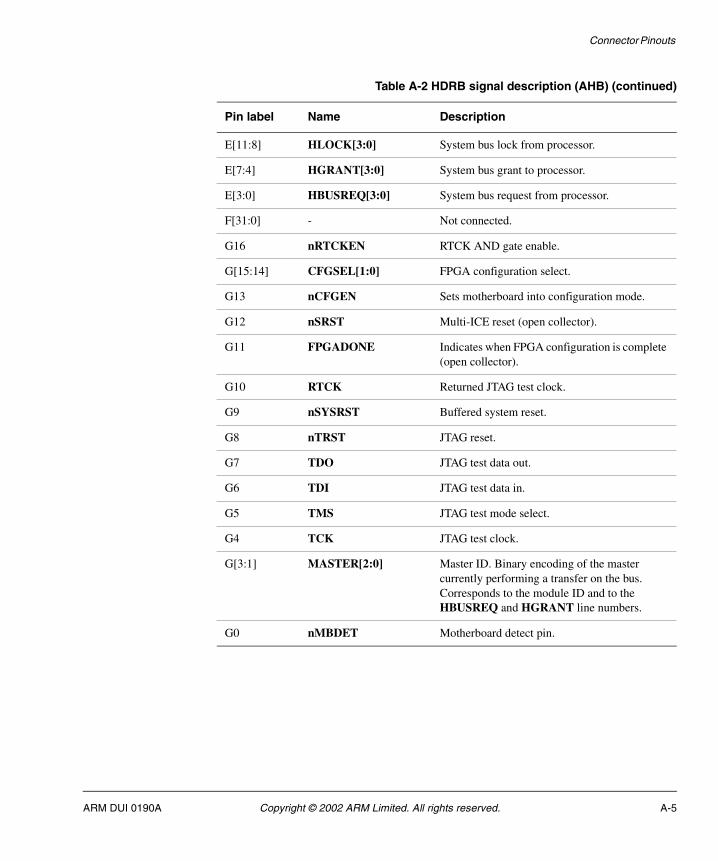
Connector Pinouts
E[11:8] HLOCK[3:0] System bus lock from processor.
E[7:4] HGRANT[3:0] System bus grant to processor.
E[3:0] HBUSREQ[3:0] System bus request from processor.
F[31:0] - Not connected.
G16 nRTCKEN RTCK AND gate enable.
G[15:14] CFGSEL[1:0] FPGA configuration select.
G13 nCFGEN Sets motherboard into configuration mode.
G12 nSRST Multi-ICE reset (open collector).
G11 FPGADONE Indicates when FPGA configuration is complete (open collector).
G10 RTCK Returned JTAG test clock.
G9 nSYSRST Buffered system reset.
G8 nTRST JTAG reset.
G7 TDO JTAG test data out.
G6 TDI JTAG test data in.
G5 TMS JTAG test mode select.
G4 TCK JTAG test clock.
G[3:1] MASTER[2:0] Master ID. Binary encoding of the master currently performing a transfer on the bus. Corresponds to the module ID and to the HBUSREQ and HGRANT line numbers.
G0 nMBDET Motherboard detect pin.
Table A-2 HDRB signal description (AHB) (continued)
Pin label Name Description
ARM DUI 0190A Copyright © 2002 ARM Limited. All rights reserved. A-5

Connector Pinouts
A.3 Motherboard and BTLM connectors EXPB
Figure A-3 shows the pin numbers of the EXPB plug on the motherboard and EXPB socket on the BTLM.
Figure A-3 EXPB socket pin numbering
Figure A-4 on page A-7 shows the pin numbers of the EXPB plug on the BTLM.
61
H2
GNDGND
F0F1
F2
GNDGND
F3
H5F4
F5
GNDGND
F6
H8F7
F8
GNDGND
F9
H11F10
F11
H14
GNDGND
F12F13
F14
GNDGND
F15
H17F16
F17
GNDGND
F18
H20F19
F20
GNDGND
F21
H23F22
F23
H0
H1
H3
H4
H6
H7
H9
H10
H12
H13
H15
H16
H18
H19
H21
H22
123456789101112131415161718192021222324252627282930313233343536373839404142434445464748495051525354555657585960
H26
GNDGND
F24F25
F26
GNDGND
F27
H29F28
F29
GNDGND
F30
J0F31
J8
GNDGND
J9
J3J10
J11
J6
GNDGND
J12J13
J14
GNDJ16
J15
3V3-12V
12V
3V3-12V
12V
3V3-12V
12V
H24
H25
H27
H28
H30
H31
J1
J2
J4
J5
J7
5V
5V
5V
62
747372717069686766656463
7576
888786858483828180797877
8990
102101100999897969594939291
103104
116115114113112111110109108107106105
117118119120
A-6 Copyright © 2002 ARM Limited. All rights reserved. ARM DUI 0190A

Connector Pinouts
Figure A-4 EXPB plug pin numbering
Table A-3 describes the signals on the pins labeled F[31:0], H[31:0], and J[15:0].
61
H2GND
GNDF0
F1F2
GNDGND
F3H5 F4
F5
GNDGND
F6
H8
F7F8
GNDGND
F9H11 F10
F11
H14GND
GNDF12
F13F14
GNDGND
F15H17 F16
F17
GNDGND
F18
H20
F19F20
GNDGND
F21H23 F22
F23
H0
H1
H3
H4
H6H7
H9H10
H12
H13
H15
H16
H18H19
H21H22
123456789101112131415161718192021222324252627282930313233343536373839404142434445464748495051525354555657585960
H26GND
GNDF24
F25F26
GNDGND
F27H29 F28
F29
GNDGND
F30
J0F31
J8
GNDGND
J9
J3J10
J11
J6
GNDGND
J12J13
J14
GNDJ16
J15
3V3-12V
12V
3V3-12V
12V
3V3-12V
12V
H24
H25
H27
H28
H30H31
J1
J2
J4
J5
J7
5V
5V
5V
62
747372717069686766656463
7576
888786858483828180797877
8990
102101100999897969594939291
103104
116115114113112111110109108107106105
117118119120
Table A-3 BTLM EXPB signal description (AHB)
Pin label Name Description
H[31:28] SYSCLK[3:0] System clock to each core logic module.
H[27:24] nEPRES[3:0] Logic module present.
H[23:20] nIRQSRC[3:0] Interrupt request from logic module 3, 2, 1, and 0 respectively.
H[19:16] - Not connected.
H[15:12] ID[3:0] Logic module stack position indicator.
H[11:8] SLOCK[3:0] System bus lock from processor 3, 2, 1, and 0 respectively (not used in ASB).
ARM DUI 0190A Copyright © 2002 ARM Limited. All rights reserved. A-7

Connector Pinouts
H[7:4] SGNT[3:0] System bus grant.
H[3:0] SREQ[3:0] System bus request.
J16 nRTCKEN RTCK AND gate enable.
J[15:14] CFGSEL[1:0] FPGA configuration select.
J13 nCFGEN Sets motherboard into configuration mode.
J12 nSRST Multi-ICE reset (open collector).
J11 FPGADONE Indicates when FPGA configuration is complete (open collector).
J10 RTCK Returned JTAG test clock.
J9 nSYSRST Buffered system reset.
J8 nTRST JTAG reset.
J7 TDO JTAG test data out.
J6 TDI JTAG test data in.
J5 TMS JTAG test mode select.
J4 TCK JTAG test clock.
J[3:1] MASTER[2:0] Master ID. Binary encoding of the master currently performing a transfer on the bus. Corresponds to the module ID and to the HBUSREQ and HGRANT line numbers.
J0 nMBDET Motherboard detect pin.
F[31:0] - These connect between the GPIO pins on the FPGA on the Integrator/AP and the FPGA on the logic module. These signals are available for your own applications.
Table A-3 BTLM EXPB signal description (AHB) (continued)
Pin label Name Description
A-8 Copyright © 2002 ARM Limited. All rights reserved. ARM DUI 0190A

Connector Pinouts
A.4 Expansion connector EXPM
Figure A-5 shows the pin numbers of the connector EXPM.
Figure A-5 EXPM connector pin numbering
Table A-4 describes the signals on the EXPM pins.
Samtec TOLC series
Pin numbers for 120-way plug,viewed from above board
1
2
3
62
61
63
Table A-4 EXPM signal description
Name Description
MA[25:0] Memory address bus.
nFLWP Flash write protect.
nFLVPP Flash Vpp enable.
nBANK[7:4] Memory bank selects for nMCS1.
nMCS[3:0] Memory chip select.
EBIEN EBI enable. Drive LOW to tristate MA[25:0], nMCSN[3:0], nMWR[3:0], and nMOE.
MCS0EN Motherboard SC0 enable/disable.
nXCS0 CS0 to module. Enabled when MCS0EN is LOW.
MEMCLK Memory clock.
MD[31:0] Memory data bus.
nMWR[3:0] Memory write strobe (active LOW).
ARM DUI 0190A Copyright © 2002 ARM Limited. All rights reserved. A-9

Connector Pinouts
nMOE Memory output enable (active LOW).
MRDY Memory ready. Drive LOW to wait processor, pull up to 3.3V for normal operation.
nSYSRST2 Buffered system reset.
Table A-4 EXPM signal description (continued)
Name Description
A-10 Copyright © 2002 ARM Limited. All rights reserved. ARM DUI 0190A

Connector Pinouts
A.5 Serial interface connectors
The pinout of the serial ports is shown in Figure A-6 and Table A-5.
Figure A-6 Serial interface connector pinout
Note The serial interfaces signals operate at RS232 signal levels.
Table A-5 Serial interface signal descriptions
Pin Signal Type Function
1 DCD Input Data carrier detect
2 Rx Input Receive
3 Tx Output Transmit
4 DTR Output Data terminal ready
5 GND - Ground
6 DSR Input Data set ready
7 RTS Output Ready to send
8 CTS Input Clear to send
9 RI - Ring indicator (Not connected on Integrator)
1
6 7 8 9
2 3 4 5
ARM DUI 0190A Copyright © 2002 ARM Limited. All rights reserved. A-11

Connector Pinouts
A.6 Multi-ICE (JTAG)
Figure A-7 shows the pinout of the Multi-ICE connector on the BTLM. For a detailed description of the JTAG signals, see JTAG signal descriptions on page 4-9.
Figure A-7 Muti-ICE connector pinout
3V33V3
GND
GND
GND
GND
GND
GND
GND
GND
GND
nTRST
TDI
TMS
TCK
RTCK
TDO
nSRST
DBGRQ
DBGACK
1
19
2
20
A-12 Copyright © 2002 ARM Limited. All rights reserved. ARM DUI 0190A

Connector Pinouts
A.7 Diagnostic connectors
This section provides the pinout of the logic analyzer connectors. Figure A-8 shows the location of pin 1 for this connector type.
Figure A-8 Logic analyzer pin 1 location
1
ARM DUI 0190A Copyright © 2002 ARM Limited. All rights reserved. A-13
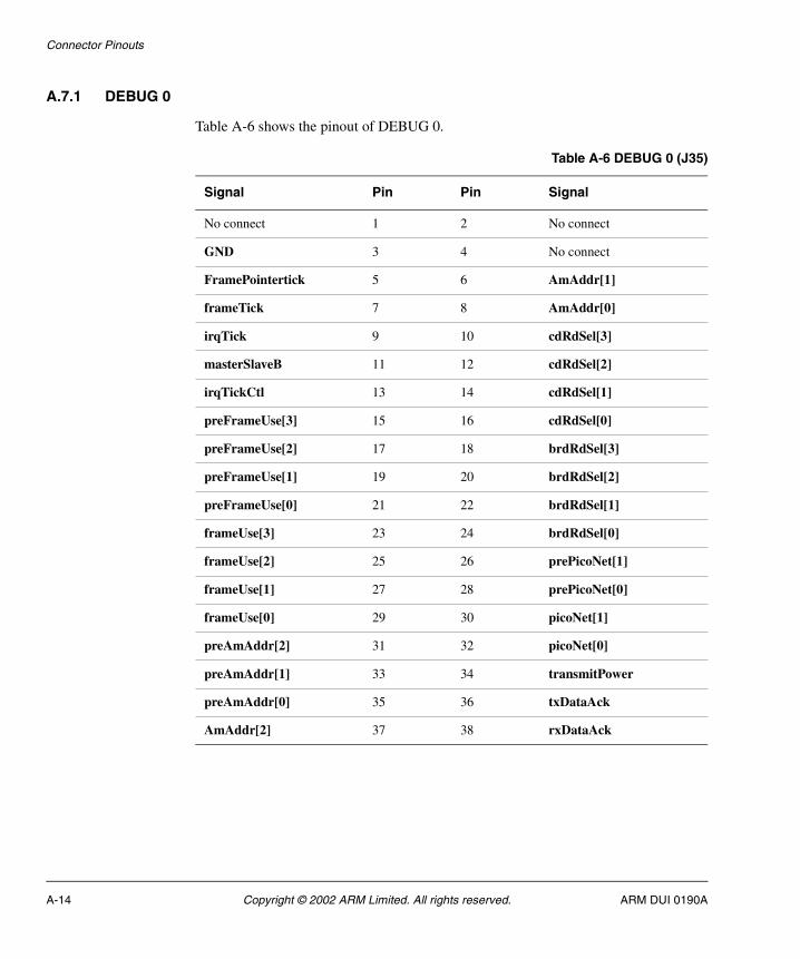
Connector Pinouts
A.7.1 DEBUG 0
Table A-6 shows the pinout of DEBUG 0.
Table A-6 DEBUG 0 (J35)
Signal Pin Pin Signal
No connect 1 2 No connect
GND 3 4 No connect
FramePointertick 5 6 AmAddr[1]
frameTick 7 8 AmAddr[0]
irqTick 9 10 cdRdSel[3]
masterSlaveB 11 12 cdRdSel[2]
irqTickCtl 13 14 cdRdSel[1]
preFrameUse[3] 15 16 cdRdSel[0]
preFrameUse[2] 17 18 brdRdSel[3]
preFrameUse[1] 19 20 brdRdSel[2]
preFrameUse[0] 21 22 brdRdSel[1]
frameUse[3] 23 24 brdRdSel[0]
frameUse[2] 25 26 prePicoNet[1]
frameUse[1] 27 28 prePicoNet[0]
frameUse[0] 29 30 picoNet[1]
preAmAddr[2] 31 32 picoNet[0]
preAmAddr[1] 33 34 transmitPower
preAmAddr[0] 35 36 txDataAck
AmAddr[2] 37 38 rxDataAck
A-14 Copyright © 2002 ARM Limited. All rights reserved. ARM DUI 0190A

Connector Pinouts
A.7.2 DEBUG 1
Table A-6 on page A-14 shows the pinout of DEBUG 1.
Table A-7 DEBUG 1 (J36)
Signal Pin Pin Signal
No connect 1 2 No connect
GND 3 4 No connect
rxFail 5 6 ctlWrData[0]
ctlRamBusy 7 8 ctlRdData[15]
ctlWrData[15] 9 10 ctlRdData[14]
ctlWrData[14] 11 12 ctlRdData[13]
ctlWrData[13] 13 14 ctlRdData[12]
ctlWrData[12] 15 16 ctlRdData[11]
ctlWrData[11] 17 18 ctlRdData[10]
ctlWrData[10] 19 20 ctlRdData[9]
ctlWrData[9] 21 22 ctlRdData[8]
ctlWrData[8] 23 24 LED[0]
ctlWrData[7] 25 26 LED[1]
ctlWrData[6] 27 28 LED[2]
ctlWrData[5] 29 30 LED[3]
ctlWrData[4] 31 32 LED[4]
ctlWrData[3] 33 34 LED[5]
ctlWrData[2] 35 36 LED[6]
ctlWrData[1] 37 38 LED[7]
ARM DUI 0190A Copyright © 2002 ARM Limited. All rights reserved. A-15

Connector Pinouts
A.7.3 DEBUG 2
Table A-6 on page A-14 shows the pinout of DEBUG 2.
Table A-8 DEBUG 2 (J37)
Signal Pin Pin Signal
No connect 1 2 No connect
GND 3 4 No connect
ctlAddr[9] 5 6 lifTxData[1]
ctlAddr[8] 7 8 lifTxData[0]
ctlAddr[7] 9 10 tyPkt[3]
ctlAddr[6] 11 12 tyPkt[2]
ctlAddr[5] 13 14 tyPkt[1]
ctlAddr[4] 15 16 tyPkt[0]
ctlAddr[3] 17 18 readLifTxData
ctlAddr[2] 19 20 broadcastSeqCh
ctlAddr[1] 21 22 airVoiceDataR[7]
ctlWr[1] 23 24 airVoiceDataR[6]
ctlWr[0] 25 26 airVoiceDataR[5]
lifTxData[7] 27 28 airVoiceDataR[4]
lifTxData[6] 29 30 airVoiceDataR[3]
lifTxData[5] 31 32 airVoiceDataR[2]
lifTxData[4] 33 34 airVoiceDataR[1]
lifTxData[3] 35 36 airVoiceDataR[0]
lifTxData[2] 37 38 putVoiceData
A-16 Copyright © 2002 ARM Limited. All rights reserved. ARM DUI 0190A
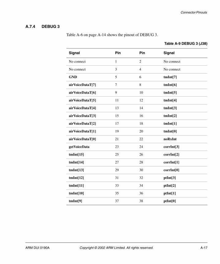
Connector Pinouts
A.7.4 DEBUG 3
Table A-6 on page A-14 shows the pinout of DEBUG 3.
Table A-9 DEBUG 3 (J38)
Signal Pin Pin Signal
No connect 1 2 No connect
No connect 3 4 No connect
GND 5 6 tmInt[7]
airVoiceDataT[7] 7 8 tmInt[6]
airVoiceDataT[6] 9 10 tmInt[5]
airVoiceDataT[5] 11 12 tmInt[4]
airVoiceDataT[4] 13 14 tmInt[3]
airVoiceDataT[3] 15 16 tmInt[2]
airVoiceDataT[2] 17 18 tmInt[1]
airVoiceDataT[1] 19 20 tmInt[0]
airVoiceDataT[0] 21 22 noRxInt
getVoiceData 23 24 corrInt[3]
tmInt[15] 25 26 corrInt[2]
tmInt[14] 27 28 corrInt[1]
tmInt[13] 29 30 corrInt[0]
tmInt[12] 31 32 ptInt[3]
tmInt[11] 33 34 ptInt[2]
tmInt[10] 35 36 ptInt[1]
tmInt[9] 37 38 ptInt[0]
ARM DUI 0190A Copyright © 2002 ARM Limited. All rights reserved. A-17

Connector Pinouts
A-18 Copyright © 2002 ARM Limited. All rights reserved. ARM DUI 0190A

Index
The items in this index are listed in alphabetical order, with symbols and numerics appearing at the end. The references given are to page numbers.
AAliased core module memory region
5-4Alphanumeric characters 5-13Alphanumeric display
control 5-13segment designation 5-14
Arbitersystem bus 3-2
Arbitration, bus 3-8Architecture
BTLM clocks 4-12interrupt controller 3-16reset 4-14
ARM email address xiAssembled Integrator system 2-2ATX PC power supply 2-5ATX power OK 3-12
BBaud rate, programming 3-20Bench power supply 2-5Block diagrams
BTLM FPGAs 4-2counter/timer 3-17GPIO 3-21interrupt controller 3-16motherboard clocks 3-14motherboard FPGA 3-2reset controller 3-11serial interface 3-19
Boot ROM 2-3Boot ROM access 5-5Boot switch 3-2Boot switch reader 5-13Bus arbitration 3-8Bus arbitration signal assignment 3-8Bus clock, system 3-14Bus interfaces 4-11Byte streamer mode 4-4
CChip selects, EBI 3-9Cipher block 4-2Clock
output divider 3-14VCO divider 3-14
Clock dividers (ICS525) 3-14Clock rate registers 3-2Clock signals 4-13Clocks
UART 3-15Clocks, motherboard 3-14Clock, reference divider 3-14CM_CTL register 5-5Code start locations 2-3Configurable clock datasheet xConnectors
EXPB A-6EXPM 5-5, A-9HDRA 2-2HDRB 2-2, A-4Multi-ICE A-12
ARM DUI 0190A Copyright © 2002 ARM Limited. All rights reserved. Index-1

Index
summary 1-9, 1-13Core module alias memory 5-4Core module interface 3-3Core module reset 3-11Core modules, attaching 2-2Counter timers 3-2Counter/timer
block diagram 3-17Counter/timer modes
free running 3-18periodic 3-18
CS_CTRL 3-13
DData masking, GPIO 3-22DebugRelFlash build 2-9Decoder status register 5-21DIL switch register 5-16DONE signal 3-12Down counter 3-17
EEBI
wait states 5-22EBI chip selects 3-9EBI memory map 5-5EBI_CSR 3-9Electromagnetic conformity iiiExpansion bus interface 5-5Expansion card present bit 5-21Expansion memory space 3-9Expansion reset 3-12EXPB connector A-6EXPM A-9EXPM connector 5-5, A-9EXPM signal description A-9External bus interface 3-2
FFCC notice iiiFeedback xiFlash access 5-5Flash programming mode 4-4
Flash Vpp bit 5-20Flash write protect bit 5-20FPGA configuration
BTLM 4-3FPGA configured 3-12FPGA DONE signal 3-11FPGA input/output pins 4-2FPGA programming 4-5FPGA register map 5-5, 5-6FPGA, description 4-2Free running mode, timer 3-18Frequency of UART clock 3-15Functional block diagram, FPGA 3-2
GGeneral purpose input output 3-2GPIO ports 3-20GPIO reads 3-23GPIO writes 3-22
HHardware resets 3-11HDRA connectors 2-2HDRB connectors 2-2, A-4HDRB signals A-4Host clock 3-14Host system clock 3-15
IInput/output, FPGA 4-2Integrator, assembled 2-2Interfaces, bus 4-11Interrupt controller 3-2
memory map 5-9registers 5-10
Interrupt controller registers 5-9
JJTAG data path 4-7JTAG signal descriptions 4-9JTAG signals 4-9, 4-18
JTAG support 4-7JTAG test reset 4-14
KKMI and timer clock 3-15
LLED control 5-13LED control register 5-15LED driver 3-2LEDs
locations 1-10, 1-15Link interface 4-2Location of LEDs 1-10, 1-15Location of test points 1-12Lock bit 5-21, 5-23Lock key 5-21, 5-23Lock register 5-21, 5-23Logic module interface 3-3Logic module reset 3-11Logic modules region 5-4
MMemory map
EBI 5-5Logic module 5-4
Memory map, system 5-2Memory size, SMI 5-23Motherboard clocks 3-14Motherboard reset 4-14Multi-ICE 3-13Multi-ICE connector 4-14Multi-ICE reset 3-11, 3-13Multi-ICE (JTAG) connector A-12
NNotices, FCC iiinPWOK signal 3-11nSRST signal 3-13
Index-2 Copyright © 2002 ARM Limited. All rights reserved. ARM DUI 0190A

Index
OOrganization of manual viiiOutput divider 3-14
PPBRST 3-12PBRST signal 3-11PCI local bus fault registers 5-21Periodic mode, timers 3-18Peripheral register region 5-5, 5-6Peripheral registers 5-7Peripherals
PrimeCell 3-17Piinouts
EXPB A-6Pinouts A-9
EXPB A-6HDRB A-4serial interface A-11
PLD programming mode 4-4Powering the Integrator/AP 2-6PrimeCell peripherals 3-17PrimeCell UART 3-2, 3-19Processor module present bit 5-21Push button 4-15Push-button reset 3-12
RReading the DIP switches 5-16Reference divider 3-14Register
summary 5-8Registers
CM_CTL 5-5LED_LIGHTS 5-15LED_SWITCHES 5-16SC_CTRLCLR 5-20SC_CTRLS 5-20SC_DEC 5-21SC_ID 5-18SC_LBFADDR 5-21SC_LOCK 5-21, 5-23SMI_CSRx 5-22TIMERx_CLR 3-18
TIMERx_CTRL 3-18TIMERx_LOAD 3-18TIMERx_VALUE 3-18UART_LCRL 3-20UART_LCRM 3-20UART_RSR 3-20
Related publications ixReprogramming the PLD 4-6Reset
core module 3-11logic module 3-11Multi-ICE 3-11signal descriptions 3-12
Reset architecture 4-14Reset control 4-14Reset controller 3-2Reset controller, motherboard 3-11Resets 3-13
software 3-13Resets, hardware 3-11ROM, RAM, and peripheral region
5-5, 5-6
SSerial interface pinout A-11Serial interface, block diagram 3-19Setting the UART baud rate 3-20Signal assignment
bus arbitration 3-8Signal descriptions
JTAG 4-9serial interface A-11
Slave serial mode 4-4SMI
wait states 5-22SMI configuration registers 5-22SMI memory size 5-23SMI_LOCK register 5-23Software reset 3-13Standby LED 2-6Summary of registers 5-8Supplying power
ATX PSU 2-5bench PSU 2-5
Switch setting, DIL 2-3System bus 3-3System bus arbiter 3-2
System bus interface 3-2System controller FPGA 3-2, 3-8System controller registers
SC_CTRLCLR 5-20SC_CTRLS 5-20SC_DEC 5-21SC_ID 5-18SC_LBFADDR 5-21SC_LOCK 5-21, 5-23
System memory map 5-2System reset 3-12System-wide FPGA configured 3-12S_VDW 5-19
TTest point functions 1-12Test points 1-12Tick interrupt interval 3-18Timer control register 3-17timer load register 3-17Timer modes 3-17
free-running 3-18periodic 3-18
Timer registersTIMERx_CLR 3-18TIMERx_CTRL 3-18TIMERx_LOAD 3-18TIMERx_VALUE 3-18
UUART 3-2, 3-19UART clock 3-15UARTCLK 3-15UART, overview 3-20UART_LCRL register 3-20UART_LCRM register 3-20UART_RSR register 3-20
VVCO divider 3-14
ARM DUI 0190A Copyright © 2002 ARM Limited. All rights reserved. Index-3

Index
WWait states, SMI 5-22Watchdog timer 3-18Write protection, SMI 3-9Writing characters to alphanumeric
display 5-13, 5-15
Index-4 Copyright © 2002 ARM Limited. All rights reserved. ARM DUI 0190A


