Download - DigitalLogic solutons.pdf

Computer Science & ITDigital Logic
WORKBOOKWORKBOOKWORKBOOKWORKBOOKWORKBOOK
2016
Detailed Explanations ofTry Yourself Questions

© Copyrightwww.madeeasypublications.org
Boolean Algebra andLogic Gates1
T1 : Solution
(b)(b)(b)(b)(b)
� � �� � � ��� � �+ + + + +x x x
= � � �� � � ���+ + +x x y x y
= � � � �+ + +x y y x
= +x y y x
= � � � �⋅x y y x
= � � � �+ ⋅ +x y y x
= +xy x y
= x y�
T2 : Solution
(d)(d)(d)(d)(d)
1When output is 1 both input can be 1.
1No input is permanantly high.

© Copyright www.madeeasypublications.org
3Workbook
T3 : Solution
(b)(b)(b)(b)(b)
Y =� � � �
� � � � � � � � �⊕ ⊕ ⊕ ⊕⊕ ⊕ ⊕ ⊕
= O ⊕ O ⊕ O ⊕ O ⊕ A= O ⊕ A
y = A
T4 : Solution
(b)(b)(b)(b)(b)F(A, B) = A ⊕ B ⎢F (x ⊕ y, z) = x ⊕ y ⊕ z
F (F (x ⊕ y, z), w) = F (x ⊕ y ⊕ z, w)= x ⊕ y ⊕ z ⊕ w
T5 : Solution
(b)(b)(b)(b)(b)
T6 : Solution
(d)(d)(d)(d)(d)P :P :P :P :P : X = Y × Z
RHSRHSRHSRHSRHS ⇒ Y × Z = �� � �+
= � � � �� � � � � �× + +
= � � � �� �� �� � �� ��+ + +
= � �� ��� � � � � �+ + +
= � ��� � � �+ +
= �� ��+= X LHSLHSLHSLHSLHS
Y = X × ZRHS:RHS:RHS:RHS:RHS: ⇒ X × Z
= �� � �+
= � � � �� � � � � �× + +
= � � � �� �� �� �� � � � � �+ + + +

© Copyrightwww.madeeasypublications.org
4 Computer Science & IT • Digital Logic
= � � �� ��� � � � � �+ + + +
= � ��� � � �+ +
= �� � �+= Y LHSLHSLHSLHSLHS
R :R :R :R :R :X × Y × Z = 1⇒ X × X
⇒ �� � �+
⇒ � �+⇒ 1
T7 : Solution
(c)(c)(c)(c)(c)A + B = 1
AB = 0
A = � ...(1)AC = BC
⇒ �� = BC
⇒ C = 0 ...(2)A + C = 1
⇒ A = 1 ...(3)B = 0 ...(4)
∴ A = 1, B = 0, C = 0
T8 : Solution
(b)(b)(b)(b)(b)P : P : P : P : P : A ⊕ B = 0 when A = B
Q : Q : Q : Q : Q : � � �+ = ⇒ � � �⋅ = ⇒ A = 1 and B = 1
R : R : R : R : R : � � �+ = ⇒ B = 0 and A = 1
S :S :S :S :S : A ⊕ B ⇒ � � � �= ⇒ ≠
T9 : Solution
(b)(b)(b)(b)(b)
x
1
A
BT
gate
A
B
T1( , 1) = x x1
2
T
gate
T2( , ) = y x y x x y = ( + )
NOR gate operation
y

© Copyright www.madeeasypublications.org
5Workbook
T10 : Solution
(d)(d)(d)(d)(d)
+ = a + b
= � �� ���+ +
= �+ += a + b + c
T11 : Solution
(a)(a)(a)(a)(a)
Ex-NOR is coincidence logic gate.
⇒ F = � �+ is coincidence logic.
F AB A B= +

© Copyrightwww.madeeasypublications.org
Number System2
T1 : Solution
(d)(d)(d)(d)(d)
(3527)8 = (01 11 01 01 01 11)2= (131113)4= (757)16
= (1879)10
So all of these.
T2 : Solution
(b)(b)(b)(b)(b)
(1217)8 = (001010001111)2= (28f)16
T3 : Solution
(d)(d)(d)(d)(d)
(66.3)8 = (110 110 011)2
T4 : Solution
(a)(a)(a)(a)(a)
Range of n bits 2’s complement numbers = –2n–1 to (2n–1 – 1)

© Copyright www.madeeasypublications.org
7Workbook
T5 : Solution
(d)(d)(d)(d)(d)A forbit 2’s complement number is to be represented as 6 bit 2’s complement number.As example: x3 x2 x1 x0 ⇒ x3 3 3 3 3 x3 3 3 3 3 x3 x2 x1 x0
T6 : Solution
(d)(d)(d)(d)(d)(135)x + (144)x = (323)x
x2 + 3x + 5 + x2+4x + 4 = 3x2 + 2x + 32x2 + 7x + 9 = 3x2 + 2x + 3
x2 + 5x – 6 = 0(x – 6)(x + 1) = 0
x = 6, x = –1 base can’t be negative.
T7 : Solution
(b)(b)(b)(b)(b)
(BA)(BA)(BA)(BA)(BA)1616161616 – (AB) – (AB) – (AB) – (AB) – (AB)16 16 16 16 16 ::::: 10111010
10101011
00001111 = (F)16
(BC)(BC)(BC)(BC)(BC)1616161616 – (CB) – (CB) – (CB) – (CB) – (CB)16 16 16 16 16 ::::: 10111100
11001011
11110001 ≠ (F)16
(CB)(CB)(CB)(CB)(CB)1616161616 – (BC) – (BC) – (BC) – (BC) – (BC)16 16 16 16 16 ::::: 11001011
10111100
00001111 ≠ (F)16
T8 : Solution
(a)(a)(a)(a)(a)
(92.1)10
10’s = 100.092.1
07.9
9’s = 99.992.1
07.8(1011.11)2
2’s = 0100.011’s = 0100.00

© Copyrightwww.madeeasypublications.org
8 Computer Science & IT • Digital Logic
T9 : Solution
(a)(a)(a)(a)(a)
Possitive number: 2’s complement is same as binary : 01111111.
T10 : Solution
(a & d)(a & d)(a & d)(a & d)(a & d)
2’s complement = 1’s complement + 1
1’s complement = 2’s complement – 1
T11 : Solution
(d)(d)(d)(d)(d)(73)x = (54)y
7x + 3 = 5y + 4x = 8 ⇒ 56 + 3
= 5y + 4y = 11
T12 : Solution
(5)(5)(5)(5)(5)
�
�= 13.1
⇒�� �
�
+ +x xx
=
�+ +xx
⇒�� �
�
+ +x xx
=
�+ +xx
⇒ 3x2 + x + 2 =�� � � �+ +/
/x x x
x⇒ 3x2 + x + 2 = 2x2 + 6x + 2⇒ x2 – 5x = 0⇒ x(x – 5) = 0⇒ (x = 5)

© Copyright www.madeeasypublications.org
9Workbook
T13 : Solution
(3)(3)(3)(3)(3)(123)5 = (x 8)y
52 + 2 × 5 + 3 = xy + 825 + 10 + 3 = xy + 8
xy = 30, y > 81. y = 10, x = 32. y = 15 , x = 13. y = 30, x = 1
T14 : Solution
(210212.2011)(210212.2011)(210212.2011)(210212.2011)(210212.2011)
(7 2 5 6 4)⋅ 9
(21 02 12 20 11)3= 210212 2011
⋅⋅
© Copyrightwww.madeeasypublications.org
K-maps3
T1 : Solution
(b)(b)(b)(b)(b)F = A + B′CF = Σ(1, 4, 5, 8, 7)
BC
0 1 3 2
4 5 7 6
A
T2 : Solution
(b)(b)(b)(b)(b)F = AD + BD Independent of C.
CD
0 1 3 2
4 5 7 6
AB
12 13 15 14
8 9 11 10
BDAD
T3 : Solution
(c)(c)(c)(c)(c)
F = �� �� �� ��+ + +
= � � � � �� �� �� ��+ + +
= � � � �� � � � � �+� �
= � �� �� � � �+ �

© Copyright www.madeeasypublications.org
11Workbook
T4 : Solution
(c)(c)(c)(c)(c)F1 = Σ(0, 1, 3, 5)F2 = Σ(4, 5)
F1 + F2 = Σ(0, 1, 3, 4, 5
� � + = Σ(0, 1, 3, 4, 5
� ���� � ������� �⎫
= Σ +⎬⎭F = Σ(1, 4, 5)
T5 : Solution
(3)(3)(3)(3)(3)
f(A, B, C) = C + AB
= (C + A) (C + B) POS from.
A
B
C
f A B C( , ),
3 NOR gates.
T6 : Solution
(c)(c)(c)(c)(c)
f1 (w, x, y, z) = � � � �+ +x x
f1 (w, x, y, z) = Σm(2, 4, 6, 9, 10, 11, 12, 14)
f1f2
f
f3
yzw,x
1 1
11
111
w
x
z
1yz
wxzxzy
Required f(w, x, y, z) = Σm(1, 3, 5, 6, 9, 12, 13)then the function f2 = Σm(6, 9, 12) + d(0, 1, 3, 5, 7, 8, 13, 15)
and �� = Σm(1, 3, 5, 13) + d(6, 9, 12)
So that f3 is f3(w, x, y, z) = Σm(0, 2, 4, 7, 8, 10, 11, 14, 15) + d(6, 9, 12)
© Copyrightwww.madeeasypublications.org
12 Computer Science & IT • Digital Logic
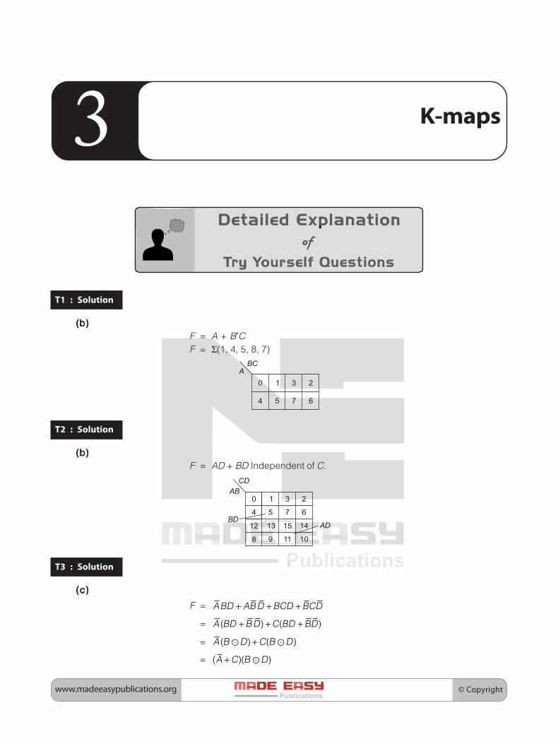
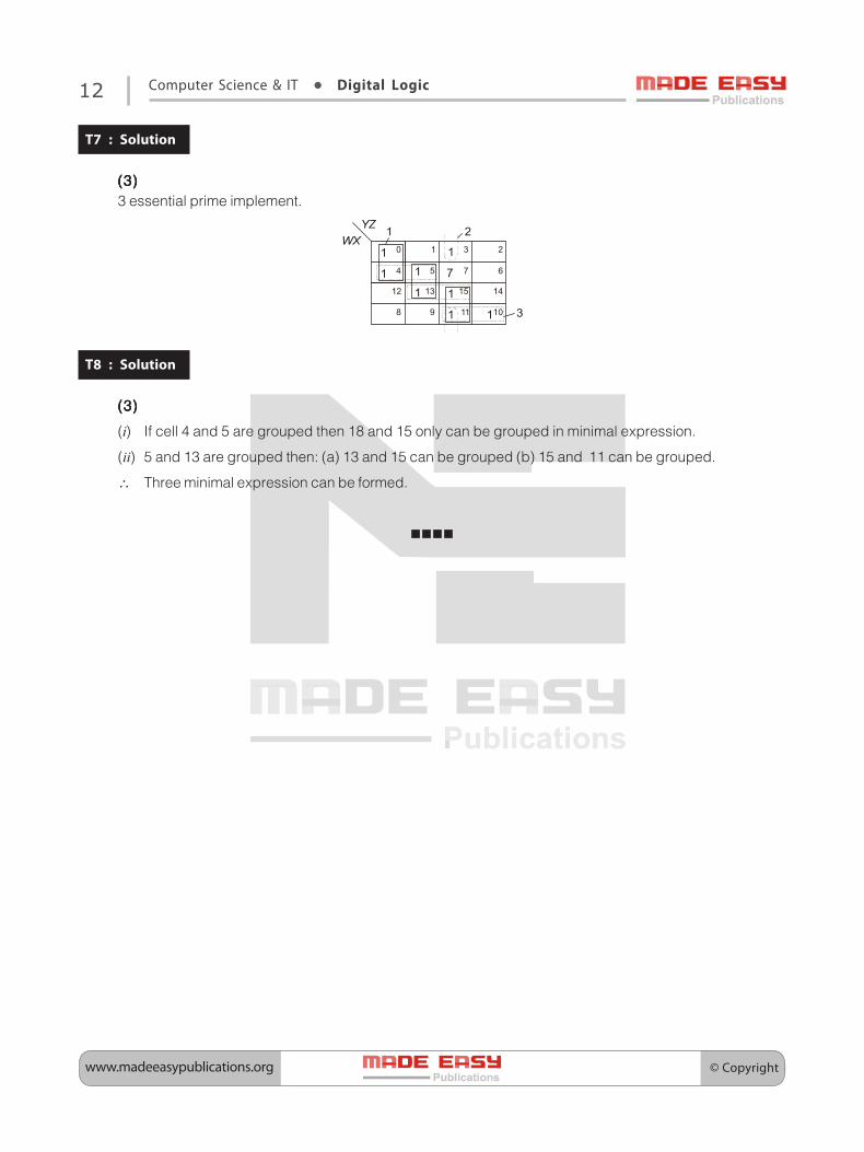
T7 : Solution
(3)(3)(3)(3)(3)3 essential prime implement.
YZ
1 0 1 1 3
22
1 4 1 5 7 7 6
WX
12 1 13 1 15 14
8 9 1 11 110 3
1
T8 : Solution
(3)(3)(3)(3)(3)
(i) If cell 4 and 5 are grouped then 18 and 15 only can be grouped in minimal expression.
(ii) 5 and 13 are grouped then: (a) 13 and 15 can be grouped (b) 15 and 11 can be grouped.
∴ Three minimal expression can be formed.

© Copyright www.madeeasypublications.org
T1 : Solution
(d)(d)(d)(d)(d)Output = Control Input + Control Input
1 Phase inverted
0 as it is passed
Output = Control ⊕ Input= EXOR gate
T2 : Solution
(a)(a)(a)(a)(a)As per the problem description for generating carry the delay is 2 time units, and 2 time units delay isinvolved for generating sum output after knowing carry. Hence the total delay is 4 time units.
Carry Circuit
Sum Circuit
2 units
2 units
T3 : Solution
(c)(c)(c)(c)(c)
A = A3 A2 A1 A0
B = B3 B2 B1 B0
A > BA > BA > BA > BA > B
(i) If A3 > B3 ⇒ � �� �
ororororor
Combination Circuit4

© Copyrightwww.madeeasypublications.org
14 Computer Science & IT • Digital Logic
(ii) A3 = B3 but A2 > B2 ⇒ (A3 � B3) � � � � �� � � � �=
(iii) A3 = B3, A2 = B2 but A1 > B1 ⇒� � � �� � � �
(iv) A3 = B3, A2 = B2, A1 = B1, but A0 > B0 ⇒� � � � � � � �
So that if A > B then the expression is
� � � � � � � � � � � � � � �� � � �� � � � �� � � � �
T4 : Solution
(b)(b)(b)(b)(b)Y = 3Y Y YX X X X
0 = 0
2 1
3 2 1
Y Y Y YX X X X
3 2 1 0
3 2 1 0 ⇒ – Y X
T5 : Solution
(b)(b)(b)(b)(b)
Carry look ahead adder is implemented using k logic levels and each logic gate delay is ‘d’.
Hence maximum delay is kd.
T6 : Solution
(c)(c)(c)(c)(c)
The occurance of overflow is indicated by the boolean function which is �� � �� �+ .
T7 : Solution
(b)(b)(b)(b)(b)
In 2’s complement addition, overflow cannot occur when a positive value is added to a negative value.
T8 : Solution
(a)(a)(a)(a)(a)
X = � �� � � � � ���� ��� ���+ +I I I
= � � �� � � �� ��� ��� � ���+ +
= ���� ��� ����+ +
= � ����� ��� � � ����+ + +
= ���� ���� ���� ����+ + +
= ��� �� ����∑

© Copyright www.madeeasypublications.org
15Workbook
T9 : Solution
(c)(c)(c)(c)(c)
Y = � � � � � � � � � � � � � � �� � � � � � � �� � � � � � � � � � � �+ + +x x x x
Y = �� � �� � �� � �� ���� ��� ��� ���+ + +
= � ���� ��� ��� ���+ + +
= � � � �⎡ ⎤ ⎡ ⎤+ + +⎣ ⎦ ⎣ ⎦
= � � � �� � � � � �+ ⊕�
= � �� � � � � �⊕ + ⊕
T10 : Solution
(a)(a)(a)(a)(a)
I00
0
1
1
I1
I2
I3 S1 S0
4-to-1MUX
I00
0
1
1
I1
I2
I3 S1 S0
4-to-1MUX Y X
CBA
Z
Z
Output of 1st 4 to 1 MUX = �� �� �+ =
Output of 2nd 4 to 1 MUX = �� ��+
= � ��� �� �+ + � ��� �� �+
= �� �� �� � � + + + ��� ���+
X = ��� ��� ��� ���+ + +
T11 : Solution
(a)(a)(a)(a)(a)
f = a, b
Using multiplier = f = � � � � �� � + ⋅ +x x x x x
� � �� � � ��� � �= = =x x x
� � �� � �� �� ��⋅ + + =

© Copyrightwww.madeeasypublications.org
16 Computer Science & IT • Digital Logic
T12 : Solution
(c)(c)(c)(c)(c)To implement n variable function we require a data selector with n – 1 select inputs and 2n–1 data inputs. Sominimum size of multiplexer needed is 2n–1 line to 1 line.
T13 : Solution
(c)(c)(c)(c)(c)A multiplexer: (i) selects one of the several inputs and transmits it to a single output. (ii) Converts paralleldata into serial data and (iii) is a combinational circuit.
T14 : Solution
(c)(c)(c)(c)(c)
Q1 =� � � �� �+I I
Q2 =� � � �� �+I I
Q =� � � �� � � �+
= ( ) ( )� � � � � � � � � �� � � � � �+ + +I I I I
=� � � � � � � � � � � �� � � � � � � �+ + +I I I I
T15 : Solution
(2)(2)(2)(2)(2)
f = ��� ���+ =�
A B
A B f=
1
0
0
A2 to 1MUX
2 to 1MUX
T16 : Solution
(d)(d)(d)(d)(d)
If A = 0, C = 0 ⇒ f = I2 = � �
If A = 0, C = 1 ⇒ f = I0 = �
If A = 1, C = 0 ⇒ f = I3 = ���
If A = 1, C = 1 ⇒ f = I1 = �f(A, B, C) = Σm(0, 1, 4)
= ���

© Copyright www.madeeasypublications.org
17Workbook
T17 : Solution
(a)(a)(a)(a)(a)
T R
0
0
1
1
0
1
0
1
f
0
1
1
1
� �
� �
X
Y
R
1
Z
MUX
Z
X
Y
R
1f
Z
T18 : Solution
(d)(d)(d)(d)(d)
When two 16-input multiplexers drive a 2-input MUX resulted 32-input MUX.
T19 : Solution
(5)(5)(5)(5)(5)
2 to 4
2 to 4
2 to 4
2 to 4
2 to 4
EN
EN
EN
EN
I1I2
I3I4
∵ 5 decoders required.

© Copyrightwww.madeeasypublications.org
18 Computer Science & IT • Digital Logic
T20 : Solution
(a)(a)(a)(a)(a)The carry generate function can be given as
Ci = Gi+Gi–1 Pi+Gi–2 Pi Pi–1 +...+ G0 Pi Pi–1...Pi ...(A)
where Gi = ai bi and Pi = ai + bi in the above equation (A)
Given: a = a2 a1 a0 and b = b2 b1 b0. The carry generate function is C2 while adding the given two 3 bitbinary numbers is
C2 = G2+G1P2 + G0+P2P1 ...(1)
Substituting G2, G1, G0, P2 and P1 values in the equation (1)
C2 = a2b2 + a1b1(a2+b2) + a0b0(a2+b2) (a1+b1)
= a2b2 + a2 a1b1 + a1 b2b1 + a0 b0 [a2 a1 + a2 b1 + a1b2 + b2 – b1]
= a2b2 + a2 a1b1 + a1 b2b1 + a2 a1a0 b0 + a2 a0 b1b0 + a1a0 b2b0 + a0b2b1b0

© Copyright www.madeeasypublications.org
Sequential Circuit5
T1 : Solution
(d)(d)(d)(d)(d)If x = 0 ⇒ Qn+1 = Qn
x = 1 ⇒ Qn+1 = ��
x TQn
Qn
∵ It is T-flipflop.
T2 : Solution
(b)(b)(b)(b)(b)
DX Q
QClock
Q Xn ⊕
If x = 0 ⇒ Qn+1 = Qn
x = 1 ⇒ Qn+1 = ��
∵ It is T-flipflop.

© Copyrightwww.madeeasypublications.org
20 Computer Science & IT • Digital Logic
T3 : Solution
(d)(d)(d)(d)(d)
00110011
00001111
00110011
01010101
110001XY
A B Q Q+
11000011
RS
S = A � B; R = BQ+(A, B, Qn) = Σm(0, 1, 5) + Q(6, 7)
=������
or =������
T4 : Solution
(a)(a)(a)(a)(a)
Case (Case (Case (Case (Case (i):):):):): Consider initially X = 1 and Y = 0B is replaced with the sequence 101010...X = 1 → 1 → 0 → 0 → 0 → 0 → 0...Y = 0 → 1 → 1 → 1 → 1 → 1...B ⇒ 1 → 0 → 1 → 0 → 1 → 0X fixed to ‘0’ and Y fixed to ‘1’.
Case (Case (Case (Case (Case (ii):):):):): Consider initially X = 0 and Y = 1X = 0 → 0 → 0 → 0 → 0 → 0 → 0...Y = 1 → 1 → 1 → 1 → 1 → 1...B ⇒ 1 → 0 → 1 → 0 → 1 → 0X fixed to ‘0’ and Y fixed to ‘1’.
T5 : Solution
(d)(d)(d)(d)(d)
1
0
1
0
1
0
1
0
↓
Μ
↓
↓
↓
↓
↓
↓
1
1
1
1
1
1
1
1
0
1
0
1
0
1
Q J = 1 K Q= n

© Copyright www.madeeasypublications.org
21Workbook
T6 : Solution
(a)(a)(a)(a)(a)
01234567
00001111
00110011
01010101
10110100
1X1X0X0X
X1X0X0X1
A B Qn Qn+1 J K
Problem is converting JK flip-flop to A-B flip-flop.
J(A, B, Qn) = Σm(0, 2) + d(1, 3, 5, 2) = �
K(A, B, Q11) = Σm(1, 7) + d(0, 2, 4, 6) = ����� = A � B
T7 : Solution
(b)(b)(b)(b)(b)
01234567
00001111
00110011
01010101
11100100
1X1X0X0X
X1X0X0X1
A B Qn Qn+1 J K
Problem is converting JK flip-flop to X-Y flip-flop.
J(X, Y, Qn) = Σm(0, 2) + d(1, 3, 5, 7) = �
K(X, Y, Qn) = Σm(3, 7) + d(0, 2, 4, 6) = Y
T8 : Solution
(b)(b)(b)(b)(b)For NAND gates: Inputs [(0,1); (1,1)]⇒ Output [(1, 0) ; (1, 0)]For NOR gates : Inputs [(0, 1); (1,1)]⇒ Output [(1,0); (0,0)]
T9 : Solution
(c)(c)(c)(c)(c)
Consider 4 bit shift register with data 01010 1 0 10 1 0 10 1 0 10 1 0 10 1 0 1 ⇒ (5)10 Left shift by one bit the data is
1 0 1 01 0 1 01 0 1 01 0 1 01 0 1 0 ⇒ (10)10 Multiplication by 2

© Copyrightwww.madeeasypublications.org
22 Computer Science & IT • Digital Logic
T10 : Solution
(7)(7)(7)(7)(7)
Clk SI Q3 Q2 Q1 Q0
1234567
1000101
11000101
01100010
10110001
01011000
Hence answer is 7.
T11 : Solution
(a)(a)(a)(a)(a)
A pulse train can be delayed by a finite number of clock periods using a serial-in-serial-out shift register.
T12 : Solution
(d)(d)(d)(d)(d)
Clk Q1Q2 Q0
12
101
010
101
01
10
J2 = Q0 K2 = Q0
After 2 clock pulses Johnsn counter is counting to intial state. Hence the frequency of output Q2Q1Q0 willbe fc / 2.
T13 : Solution
(d)(d)(d)(d)(d)
DDDDDAAAAA= Q= Q= Q= Q= QDDDDD ⊕ ⊕ ⊕ ⊕ ⊕ QQQQQCCCCC
Clk Q D ← Q Q QC B A← ← QA
123→
0001
0010
0100
1001
0001
Clk Q D ← Q Q QC B A← ← QA
→ 100
01
11
10 0
∴ Not matching to the given sequence.
∴ Not matching to the given sequence.
Clk Q D ← Q Q QC B A← ← QA
→ 111
11
10
00 0
∴ Not matching to the given sequence.
© Copyright www.madeeasypublications.org
23Workbook
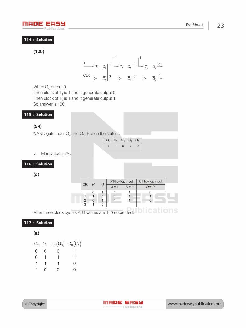
T14 : Solution
(100)(100)(100)(100)(100)
T0 Q0
Q0
T1 Q1
Q1
T2 Q2
Q2CLK
11 1
0 0
11
1
0
When Q0 output 0.Then clock of T1 is 1 and it generate output 0.Then clock of T2 is 1 and it generate output 1.So answer is 100.
T15 : Solution
(24)(24)(24)(24)(24)
NAND gate input Q4 and Q3. Hence the state is
Q4 Q3 Q2 Q1 Q0
1 1 0 0 0
∴ Mod value is 24.
T16 : Solution
(d)(d)(d)(d)(d)
123
0101
P QClkJ = 1 K = 1 D P=
P Flip-flop input Q Flip-flop input
1010
111
111
010
After three clock cycles P, Q values are 1, 0 respected.
T17 : Solution
(a)(a)(a)(a)(a)
( ) ( )� � � � � �� � � � � �
� � � �
� � � �
� � � �
� � � �

© Copyrightwww.madeeasypublications.org
24 Computer Science & IT • Digital Logic
T18 : Solution
(c)(c)(c)(c)(c)Initially cleared so q2 q1 q0 = 000
Clock Data q0 = Data q q q1 0 2+ = ⊕ q q2 1=
1st
23456789
nd
rd
th
th
th
th
th
th
100110000
100110000
010110101
001011010
At 9th clock pulse 010 will be present.
T19 : Solution
(d)(d)(d)(d)(d)
Clock Q0 Q1FF0 FF1
D = Q0 0 D = Q Q1 1 0⊕
1234
01010
01100
1010
1100
Initial state
The state sequence is00 11 01 10
T20 : Solution
(a)(a)(a)(a)(a)A shift register can be used for parallel to serial conversion.A multiplexer can be used as a many to one switch.A decoder can be used to generate memory chip select.
T21 : Solution
(c)(c)(c)(c)(c)Consider the propagation delay of each flip-flop as tp.n stage syndroms counter delay = tp (here 20 nsec)n stage asynchronous (ripple) counter delay = ntp (here 4 × 20 nsec = 80 nsec)

© Copyright www.madeeasypublications.org
25Workbook
T22 : Solution
(c)(c)(c)(c)(c)
n-bit
�
�
�
��
�
�
�
�
�
�
�
�
�
�
�
�
�
�
�
�
�
�
�
�
�
�
�
�
�
�
���
���
�����
�
�
�
���
�
Ring counter of 2 bitsn
T23 : Solution
(40)(40)(40)(40)(40)10 bit ring counter is divided by 10 counter4 bit parallel counter is divided by 16 counterMod 25 ripple counter is divided by 25 counter4 bit Johnson counter is divided by 8 counterInput clock frequency = 160 kHz.
W =��
�����
=
X =�
����
=
Y =���
�� ��
=
T24 : Solution
(c)(c)(c)(c)(c)Count = 1, load = 0 externally connected to the counter. Based on the function table, whenever clear inputis ‘0’ the counter will increment its value by one and whenever clear input is 1, all the flip-flops is the counterwill get value as ‘0’.
Clock A4
Initial state 12345
0000000
Clear = A ⋅ 3 1AA3 A2 A1
0000110
0011000
0101010
000001Transition
Hence the switching sequence is 0, 1, 2, 3, 4.
T25 : Solution
(d)(d)(d)(d)(d)
� �
!
�"
� � � # �
��!$%& &�' � �
��!$%& &�'


