© Synopsys 2013 1
Digital Integrated Circuits
Design Flow
Victor Grimblatt
R&D Group Director
August 2013
© Synopsys 2013 2
• Introduction
• CMOS Technology
• ASIC Design Flow
• Best Practices
Agenda

© Synopsys 2013 3
Introduction
© Synopsys 2013 4
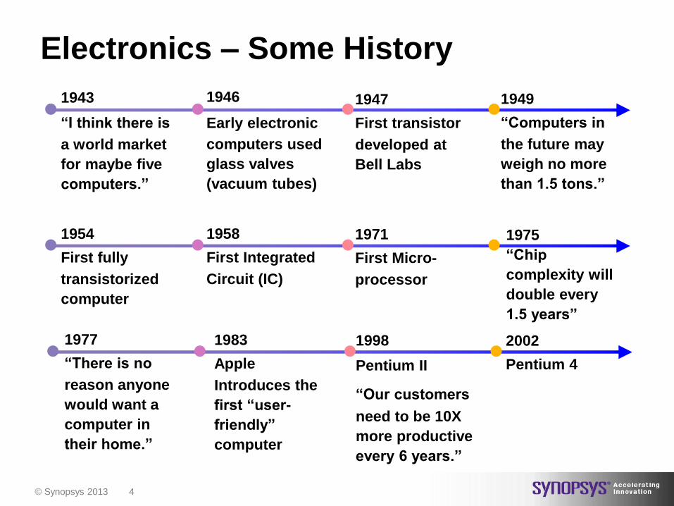
Electronics – Some History
1943
“I think there is
a world market
for maybe five
computers.”
1946
Early electronic
computers used
glass valves
(vacuum tubes)
1947
First transistor
developed at
Bell Labs
1949
“Computers in
the future may
weigh no more
than 1.5 tons.”
1954
First fully
transistorized
computer
1958
First Integrated
Circuit (IC)
1971
First Micro-
processor
1977
“There is no
reason anyone
would want a
computer in
their home.”
1983
Apple
Introduces the
first “user-
friendly”
computer
1998
Pentium II
“Our customers
need to be 10X
more productive
every 6 years.”
1975
“Chip
complexity will
double every
1.5 years”
2002
Pentium 4

© Synopsys 2013 5
How can you put 100 million
switches on a chip the size of
your fingernail?
Smaller is More
Make them really small!

© Synopsys 2013 6
How Do You Make a Chip?
steps

© Synopsys 2013 7
How Do You Make a Chip?
Grow a giant crystal of sand (silicon)
© Synopsys 2013 8
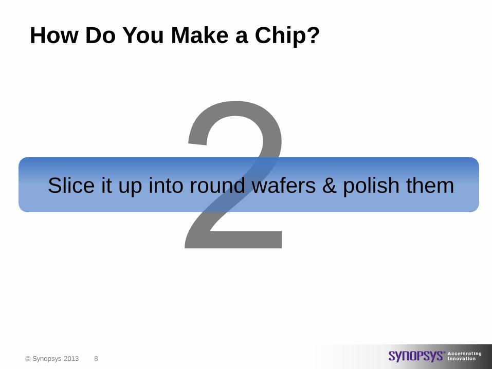
How Do You Make a Chip?
Slice it up into round wafers & polish them
© Synopsys 2013 9
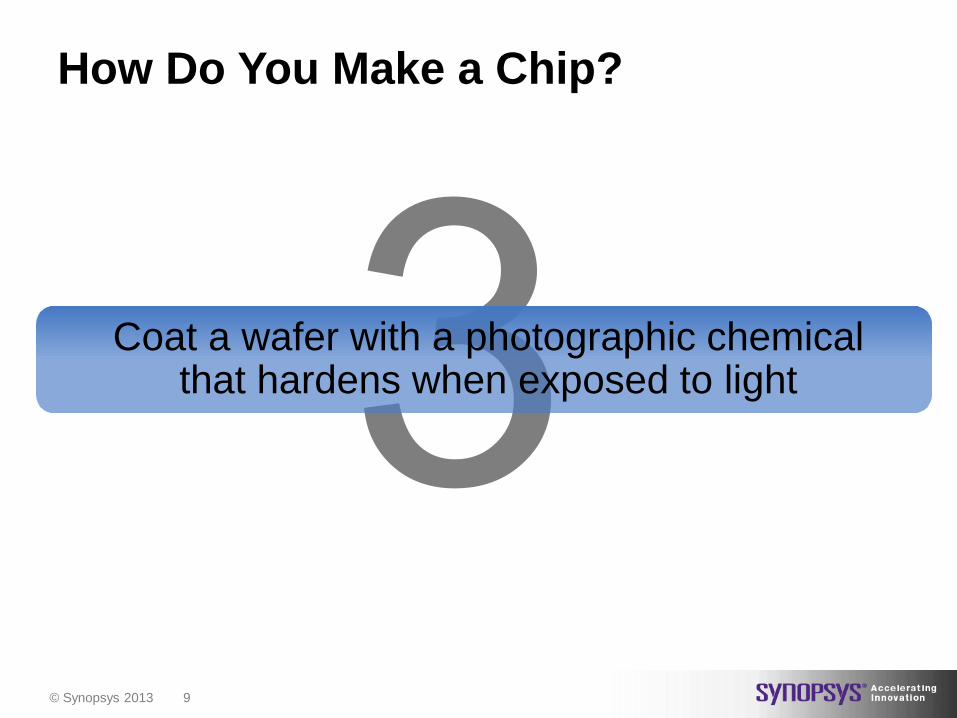
How Do You Make a Chip?
Coat a wafer with a photographic chemical that hardens when exposed to light
© Synopsys 2013 10
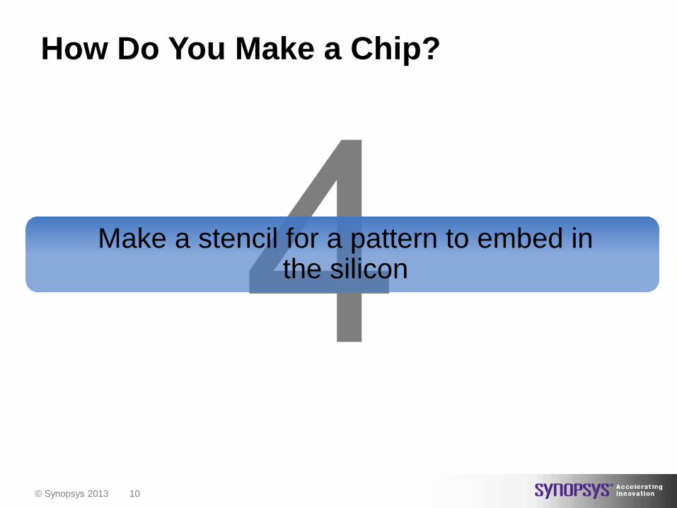
How Do You Make a Chip?
Make a stencil for a pattern to embed in the silicon
© Synopsys 2013 11
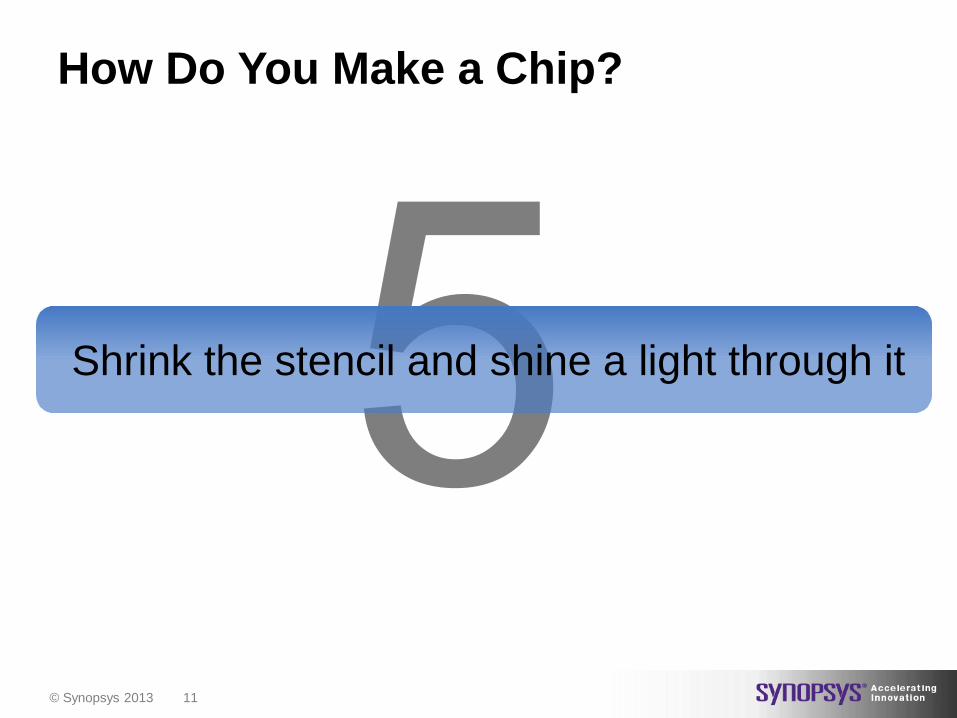
How Do You Make a Chip?
Shrink the stencil and shine a light through it
© Synopsys 2013 12
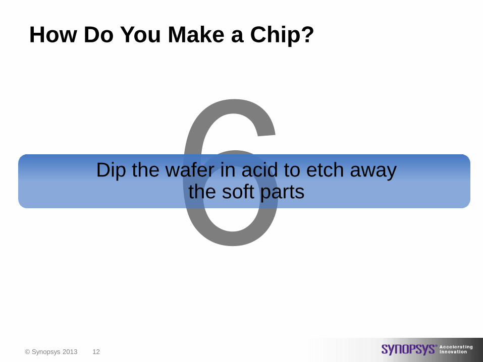
How Do You Make a Chip?
Dip the wafer in acid to etch away the soft parts

© Synopsys 2013 13
How Do You Make a Chip?
(cool term: Photolithography)
Repeat steps 3 - 6 many times, producing layers of patterns etched into the wafer
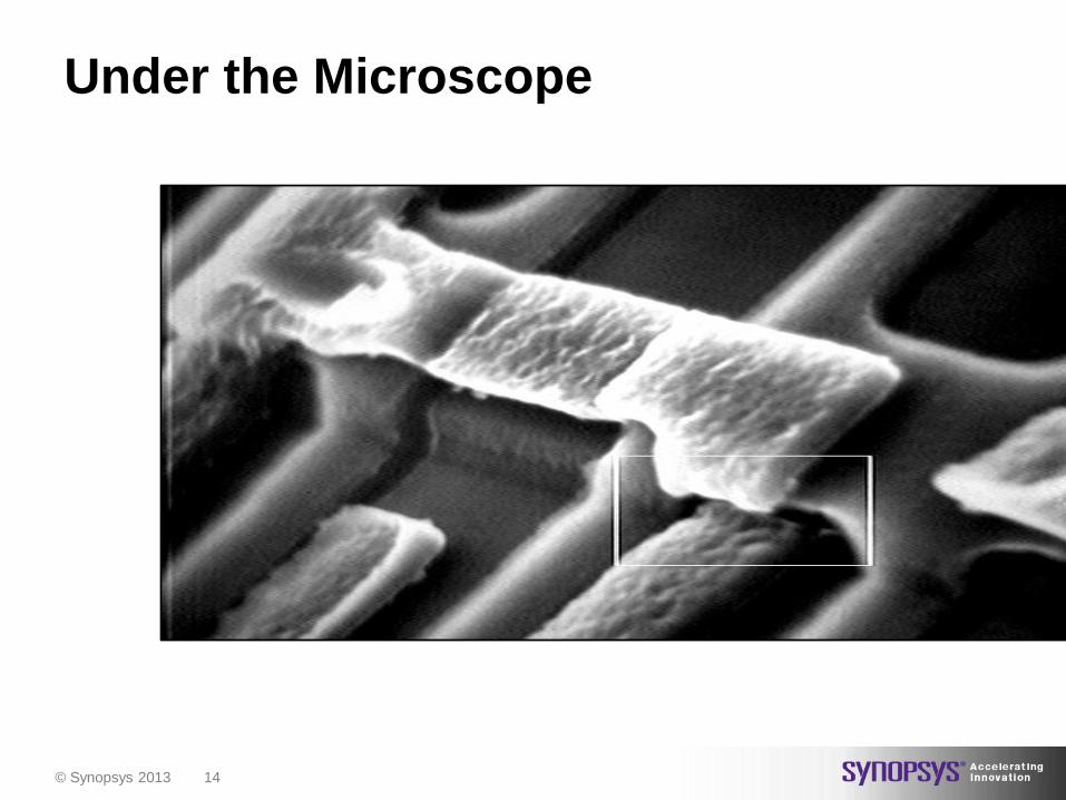
© Synopsys 2013 14
Under the Microscope

© Synopsys 2013 15
Look at the Layers
© Synopsys 2013 16
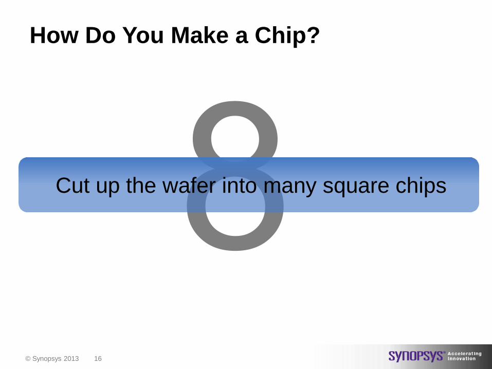
How Do You Make a Chip?
Cut up the wafer into many square chips
© Synopsys 2013 17
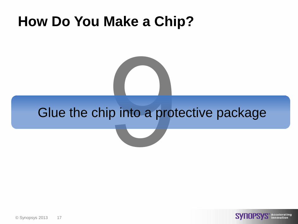
How Do You Make a Chip?
Glue the chip into a protective package

© Synopsys 2013 18
How Do You Make a Chip?
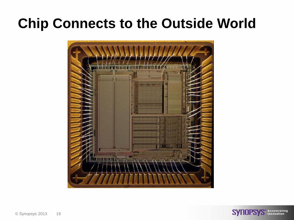
Connect the chip to the pins of the package with tiny gold wires
© Synopsys 2013 19
Chip Connects to the Outside World
© Synopsys 2013 20
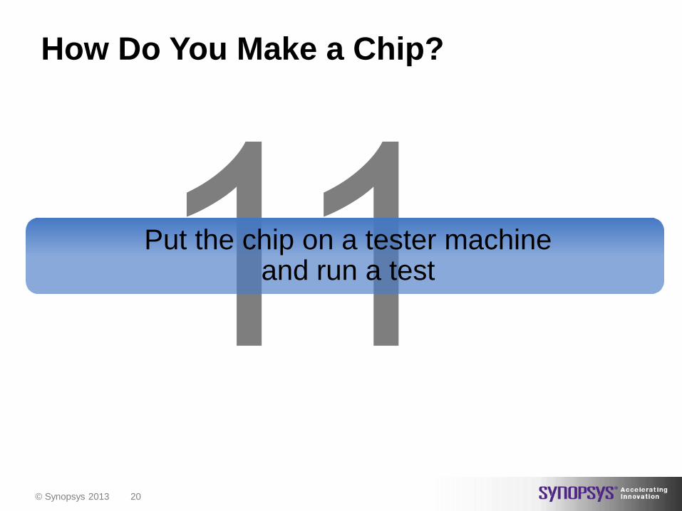
How Do You Make a Chip?
Put the chip on a tester machine and run a test
© Synopsys 2013 21
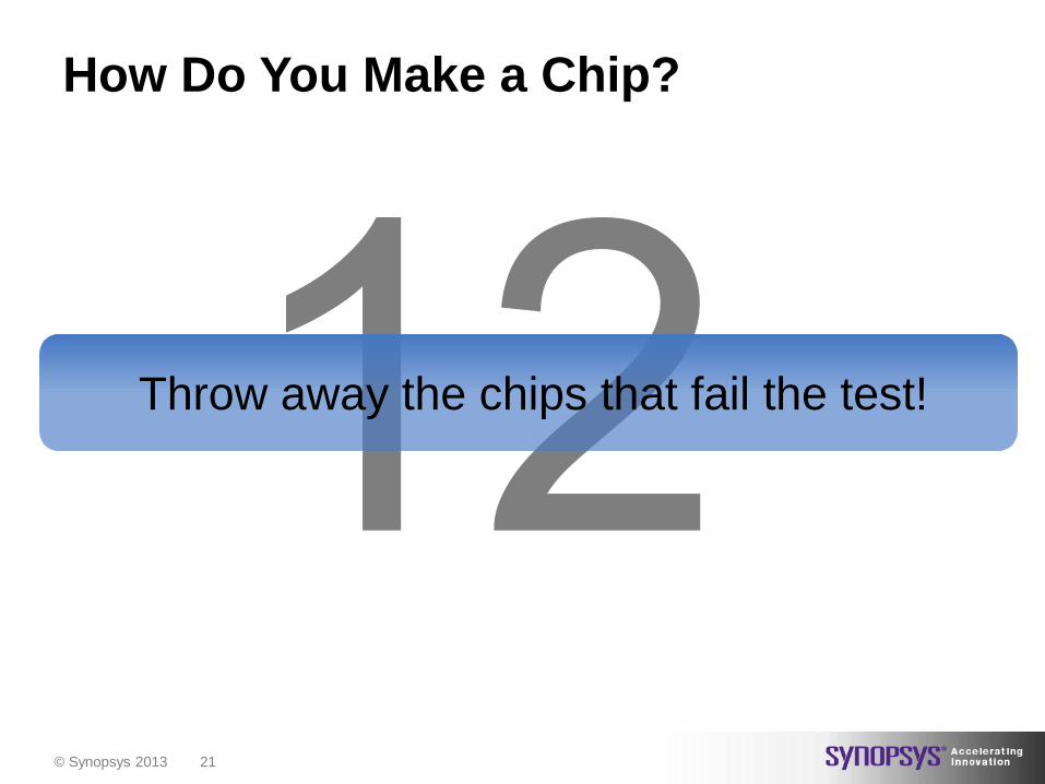
How Do You Make a Chip?
Throw away the chips that fail the test!
© Synopsys 2013 22
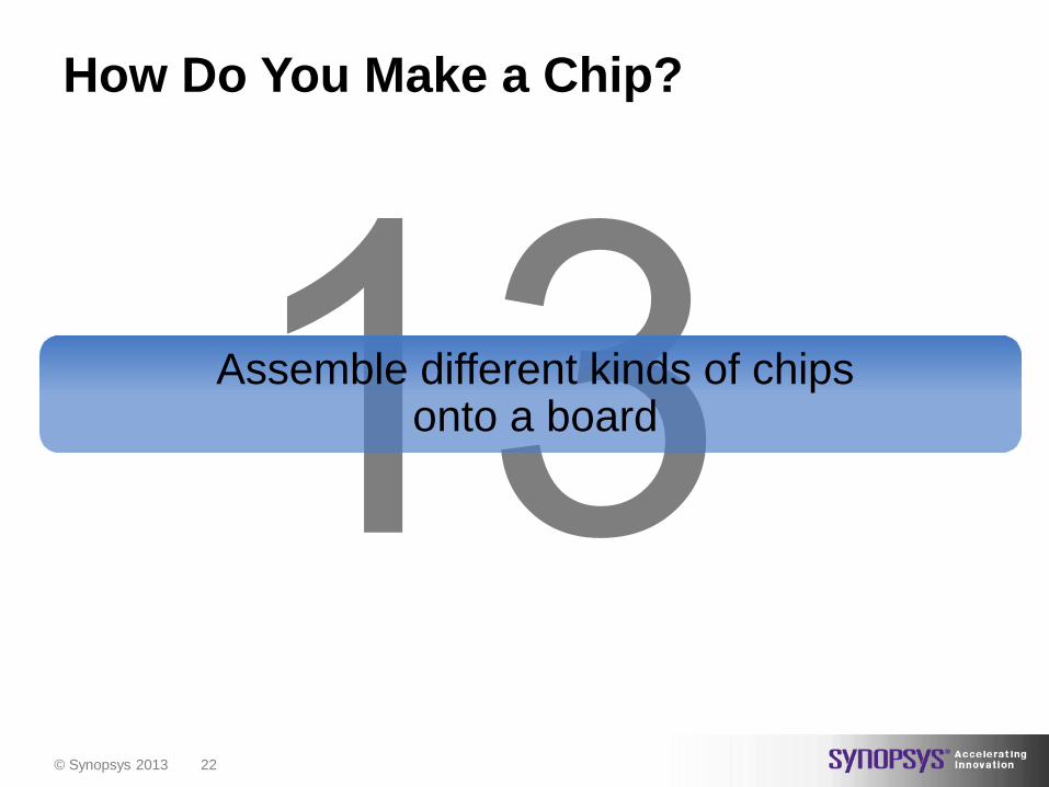
How Do You Make a Chip?
Assemble different kinds of chips onto a board
© Synopsys 2013 23
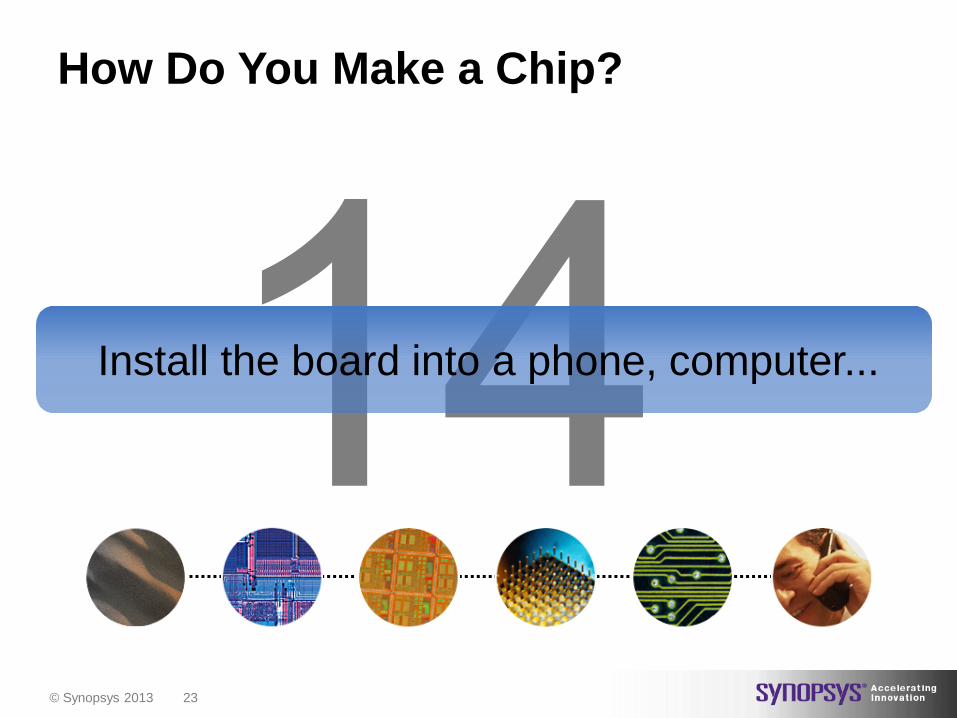
How Do You Make a Chip?
Install the board into a phone, computer...
© Synopsys 2013 24
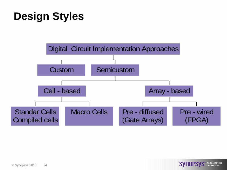
Design Styles
Custom
Standar CellsCompiled cells
Macro Cells
Cell - based
Pre - diffused(Gate Arrays)
Pre - wired(FPGA)
Array - based
Semicustom
Digital Circuit Implementation Approaches
© Synopsys 2013 25
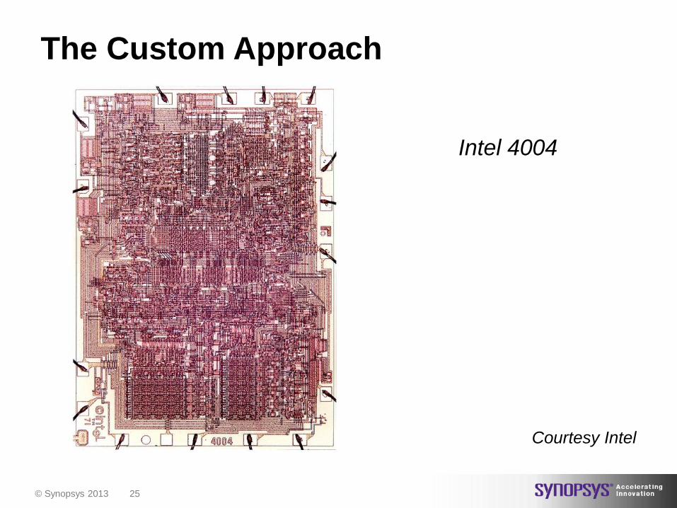
The Custom Approach
Intel 4004
Courtesy Intel
© Synopsys 2013 26
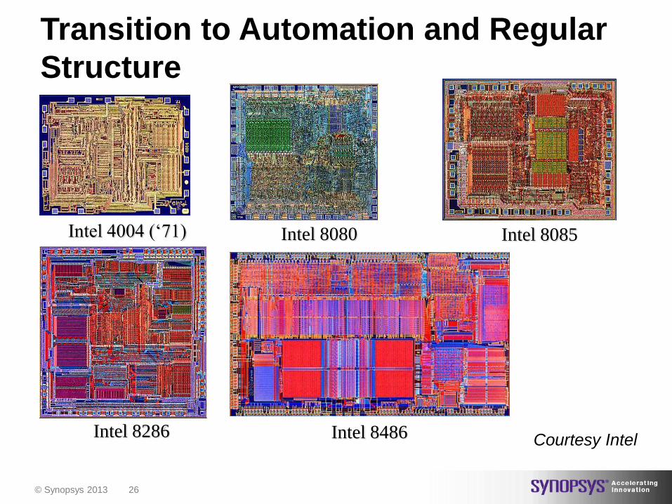
Transition to Automation and Regular
Structure
Courtesy Intel
Intel 4004 (‘71) Intel 8080 Intel 8085
Intel 8286 Intel 8486
© Synopsys 2013 27
• ASIC (Application Specific Integrated Circuit)
• General Purpose Integrated Circuits
Types of Circuits

© Synopsys 2013 28
• A chip designed to perform a particular operation
• Generally not software programmable to perform
different tasks
• Often has an embedded CPU
• May be implemented in FPGA
ASIC
© Synopsys 2013 29
• Video processor to decode or encode MPEG-2 digital TV
signals
• Encryption processor for security
• Many examples of graphical chips
• Network processor for managing packets, traffic flow,
etc.
Examples of ASIC
© Synopsys 2013 30
• Every cell and transistor is designed by hand from
scratch
• Only way to design analog portions of ASICs
• Highest performance but longest design time
• Full set of masks required for fabrication
Full Custom ASICs

© Synopsys 2013 31
• Designer uses predesigned logic cells (e.g. AND, NAND)
• Designers save time, money, and reduce risk
• Standards cells can be optimized individually
• Standard cells library is designed using full custom
• Some standar cells, such as RAM and ROM, and some
datapath cells (e.g. multiplier) are tiled together to create
macrocells
Standard Cell ASICs (semi custom)

© Synopsys 2013 32
• Transistors are predefined in the silicon wafer
• Predefined pattern of transistors is called “base array”
• Smallest element is called “base cell”
• Base cell layout is the same for each logic cell
• Only interconnection between cells and inside the cell is
customized
• Slower than cell based designs but implementation time
is faster (less time in factory)
Gate Array ASICs

© Synopsys 2013 33
CMOS Technology
© Synopsys 2013 34
CMOS Technology
• Complementary Metal Oxide Semiconductor
• Consists of NMOS and PMOS transistors
• MOS (Metal Oxide Semiconductor) Field Effect transistor
© Synopsys 2013 35
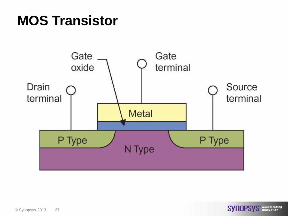
MOS Transistor
• Basic element in the design
• Voltage controlled device
• It is formed by layers
– Semiconductor layer
– Silicon dioxide layer
– Metal layer
• Consists in three regions
– Source
– Drain
– Gate

© Synopsys 2013 36
• Source and drain are quite similar
• Source is the node which acts as the source of charge
carriers
• Charge carriers leave the source and travel to the drain
• Source is the more negative terminal in N channel MOS,
it is the more positive terminal in P channel MOS
• Area under the gate is called the “channel”
MOS Transistor
© Synopsys 2013 37
MOS Transistor
© Synopsys 2013 38
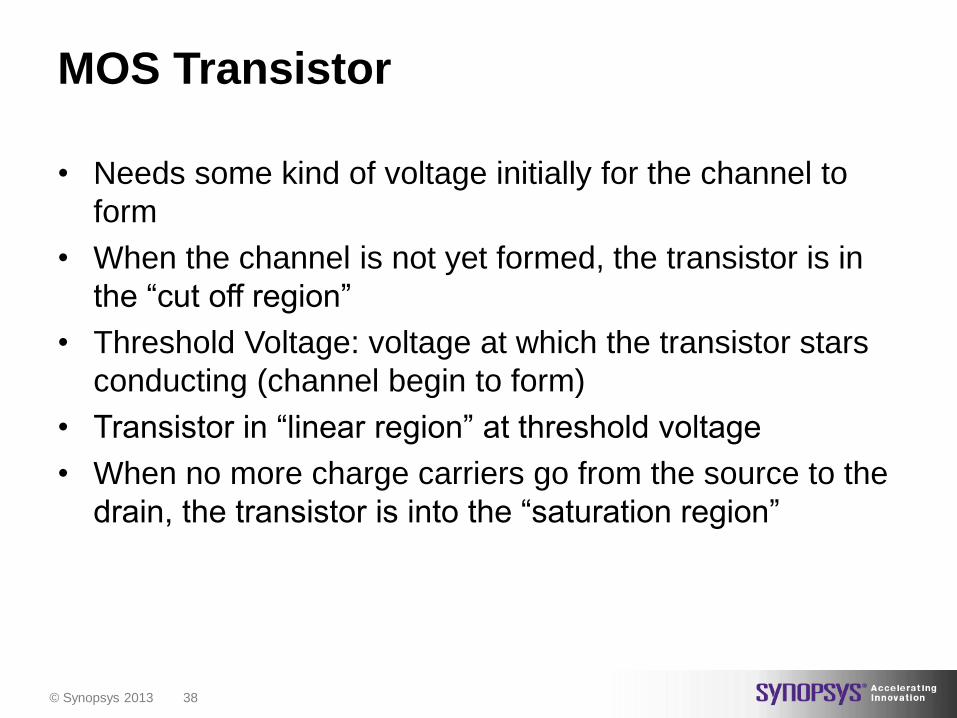
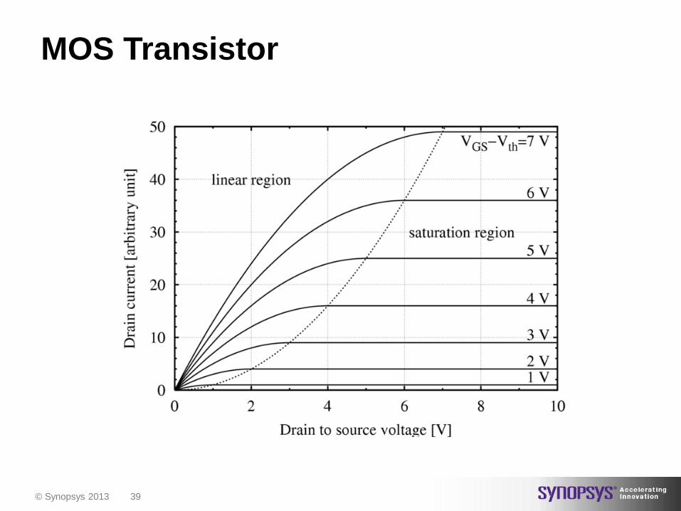
• Needs some kind of voltage initially for the channel to
form
• When the channel is not yet formed, the transistor is in
the “cut off region”
• Threshold Voltage: voltage at which the transistor stars
conducting (channel begin to form)
• Transistor in “linear region” at threshold voltage
• When no more charge carriers go from the source to the
drain, the transistor is into the “saturation region”
MOS Transistor
© Synopsys 2013 39
MOS Transistor
© Synopsys 2013 40
• Made up of both NMOS and CMOS transistors
• CMOS logic devices are the most common devices used
today in IC design
– High density
– Low power
– High operating clock speed
– Ease of implementation at the transistor level
• Only one driver but gates can drive as many gates as
possible
• Gates output always drives another CMOS gate input
CMOS Technology
© Synopsys 2013 41
• Requires one PMOS and one NMOS transistors
• NMOS provides the switch connection to ground when
the input is logic high Output load is discharged and
output is driven to logic “0”
• PMOS transistor provides the connection to power
supply (VDD) when the input is logic low Output load is
charged and output is driven to logic “1”
CMOS Inverter
© Synopsys 2013 42
• “Holes” are the charge carriers for PMOS transistors
• Electrons are the charge carriers for NMOS transistors
• Mobility of electrons is 2 times than that of “holes”
• Output rise and fall time is different between PMOS and
NMOS transistors
• To adjust time PMOS W/L ratio is about twice NMOS W/L
ratio
CMOS Technology

© Synopsys 2013 43
• L is always constant in a standard cell library
• W changes to have different drive strengths
• Resistance is proportional to L/W increasing the width
decreases resistance
CMOS Technology
© Synopsys 2013 44
• Big percentage is due to the charging and discharging of
capacitors
• Low power design are techniques used to reduce power
dissipation
Power Dissipation
© Synopsys 2013 45
Sources of Power Dissipation
• Dynamic Switching Power: Due to charge and discharge
of capacitances
– Low to high output transition draws energy from the power supply
– High to low transition dissipates energy stored in CMOS
transistor
– Total power drawn = load capacitance*VDD2*f
• Short Circuit Current: Occurs when the rise/fall time at
the input of the gate is larger than the output rise/fall time
© Synopsys 2013 46
Sources of Power Dissipation
• Leakage Current Power: Caused by 2 reasons
– Reverse-Bias diode leakage on transistor drains. It happens
when one transistor is off, and the active one charges up/down
the drain using the bulk potential of the other transistor
– Sub-Threshold leakage through the channel to an “OFF”
transistor/device

© Synopsys 2013 47
• Consists of a PMOS transistor connected in parallel to a
NMOS transistor
• Transmits the value at the input to the output
• PMOS transmits a strong 1
• NMOS transmits a strong 0
• Advantages
– Better characteristics than a switch
– Resistance of the circuit is reduced (transistors in parallel)
Transmission Gate
© Synopsys 2013 48
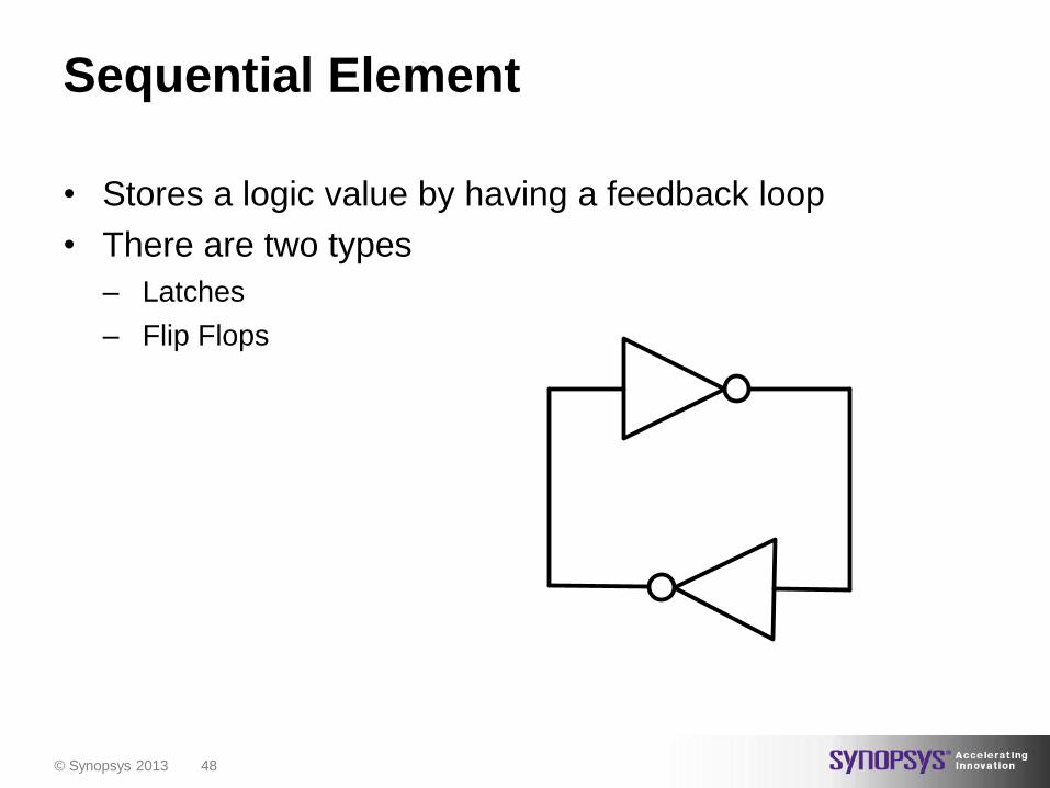
• Stores a logic value by having a feedback loop
• There are two types
– Latches
– Flip Flops
Sequential Element

© Synopsys 2013 49
• Asynchronous element
• When G is high, transmission gate is switched on and
input D passes to the output
• When G is low, transmission gate is off an inverters hold
the value
Latches
D
G
Q
© Synopsys 2013 50
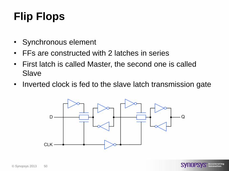
• Synchronous element
• FFs are constructed with 2 latches in series
• First latch is called Master, the second one is called
Slave
• Inverted clock is fed to the slave latch transmission gate
Flip Flops

© Synopsys 2013 51
ASIC Design Flow
© Synopsys 2013 52
• Speed
• Area
• Power
• Time to market
Design Objectives
© Synopsys 2013 53
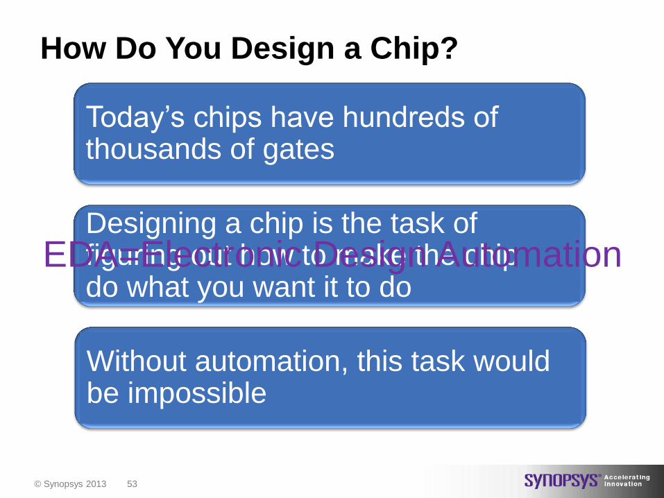
Today’s chips have hundreds of thousands of gates
Without automation, this task would be impossible
Designing a chip is the task of figuring out how to make the chip do what you want it to do
EDA=Electronic Design Automation
How Do You Design a Chip?

© Synopsys 2013 54
What’s a Design Flow?
…the steps you take to design a chip! Technology
Process
Blah blah blah
yada yada
Blah blah blah
yidie yadie
So on and so forth
on and on
Jibber jabber jibber
just jawing
Yackety yack
Ya'll com back
Blah blah blah
yada yada
Blah blah blah
yidie yadie
So on and so forth
on and on
Jibber jabber jibber
just jawing
Yackety yack
Ya'll com back
Blah blah blah
yada yada
Blah blah blah
yidie yadie
So on and so forth
on and on
Jibber jabber jibber
just jawing
Yackety yack
Ya'll com back
Gate-level
netlist
Testbench
Blah blah blah
yada yada
Blah blah blah
yidie yadie
So on and so forth
on and on
Jibber jabber jibber
just jawing
Yackety yack
Ya'll com back
Blah blah blah
yada yada
Blah blah blah
yidie yadie
So on and so forth
on and on
Jibber jabber jibber
just jawing
Yackety yack
Ya'll com back
Blah blah blah
yada yada
Blah blah blah
yidie yadie
So on and so forth
on and on
Jibber jabber jibber
just jawing
Yackety yack
Ya'll com back
Specification
Blah blah blah
yada yada
Blah blah blah
yidie yadie
So on and so forth
on and on
Jibber jabber jibber
just jawing
Yackety yack
Ya'll com back
Blah blah blah
yada yada
Blah blah blah
yidie yadie
So on and so forth
on and on
Jibber jabber jibber
just jawing
Yackety yack
Ya'll com back
Blah blah blah
yada yada
Blah blah blah
yidie yadie
So on and so forth
on and on
Jibber jabber jibber
just jawing
Yackety yack
Ya'll com back
Scripts
Initial constraints
System
Analysis System Studio
Saber
Select
Architecture
Module Compiler
Models / IP Library Compiler
DesignWare IP
VERA
RTL Verification
VCS-MX
ATPG
TetraMAX
Synthesis
Design Compiler
Power Compiler
DFT Compiler
Gate-level
verification
VCS-MX
Magellan
Formality
PrimeTime
PrimePower
Place & Route
IC Compiler
Physical Compiler
Astro
Links-to-
Layout Design Planning
PrimeTime
NanoSim
HSPICE
Post-Route
Verification
Physical Data
Creation
Blah blah blah
yada yada
Blah blah blah
yidie yadie
So on and so forth
on and on
Jibber jabber jibber
just jawing
Yackety yack
Ya'll com back
Blah blah blah
yada yada
Blah blah blah
yidie yadie
So on and so forth
on and on
Jibber jabber jibber
just jawing
Yackety yack
Ya'll com back
Blah blah blah
yada yada
Blah blah blah
yidie yadie
So on and so forth
on and on
Jibber jabber jibber
just jawing
Yackety yack
Ya'll com back GDSII
JupiterXT
Proteus
Physical Design
Checks STAR-RCXT
Hercules
RTL Gates
Design
Constraints
Mask Writer
CATS

© Synopsys 2013 55
Technology
Process
Blah blah blah
yada yada
Blah blah blah
yidie yadie
So on and so forth
on and on
Jibber jabber jibber
just jawing
Yackety yack
Ya'll com back
Blah blah blah
yada yada
Blah blah blah
yidie yadie
So on and so forth
on and on
Jibber jabber jibber
just jawing
Yackety yack
Ya'll com back
Blah blah blah
yada yada
Blah blah blah
yidie yadie
So on and so forth
on and on
Jibber jabber jibber
just jawing
Yackety yack
Ya'll com back
Gate-level
netlist
Testbench
Blah blah blah
yada yada
Blah blah blah
yidie yadie
So on and so forth
on and on
Jibber jabber jibber
just jawing
Yackety yack
Ya'll com back
Blah blah blah
yada yada
Blah blah blah
yidie yadie
So on and so forth
on and on
Jibber jabber jibber
just jawing
Yackety yack
Ya'll com back
Blah blah blah
yada yada
Blah blah blah
yidie yadie
So on and so forth
on and on
Jibber jabber jibber
just jawing
Yackety yack
Ya'll com back
Specification
Blah blah blah
yada yada
Blah blah blah
yidie yadie
So on and so forth
on and on
Jibber jabber jibber
just jawing
Yackety yack
Ya'll com back
Blah blah blah
yada yada
Blah blah blah
yidie yadie
So on and so forth
on and on
Jibber jabber jibber
just jawing
Yackety yack
Ya'll com back
Blah blah blah
yada yada
Blah blah blah
yidie yadie
So on and so forth
on and on
Jibber jabber jibber
just jawing
Yackety yack
Ya'll com back
Scripts
Initial constraints
System
Analysis System Studio
Saber
Select
Architecture
Module Compiler
Models / IP Library Compiler
DesignWare IP
VERA
RTL Verification
VCS-MX
ATPG
TetraMAX
Synthesis
Design Compiler
Power Compiler
DFT Compiler
Gate-level
verification
VCS-MX
Magellan
Formality
PrimeTime
PrimePower
Place & Route
IC Compiler
Physical Compiler
Astro
Links-to-
Layout Design Planning
PrimeTime
NanoSim
HSPICE
Post-Route
Verification
Physical Data
Creation
Blah blah blah
yada yada
Blah blah blah
yidie yadie
So on and so forth
on and on
Jibber jabber jibber
just jawing
Yackety yack
Ya'll com back
Blah blah blah
yada yada
Blah blah blah
yidie yadie
So on and so forth
on and on
Jibber jabber jibber
just jawing
Yackety yack
Ya'll com back
Blah blah blah
yada yada
Blah blah blah
yidie yadie
So on and so forth
on and on
Jibber jabber jibber
just jawing
Yackety yack
Ya'll com back GDSII
JupiterXT
Proteus
Physical Design
Checks STAR-RCXT
Hercules
RTL Gates
Design
Constraints
Mask Writer
CATS
Design Implementation:
Logical
Design Implementation:
Physical
Design for Manufacturing
Verification
© Synopsys 2013 56
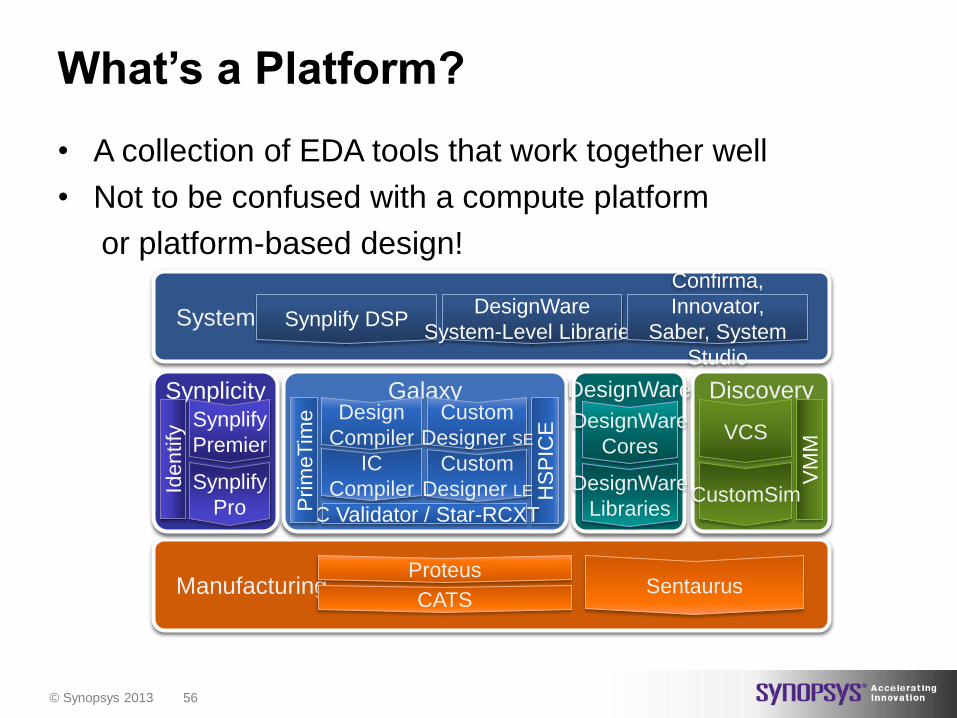
What’s a Platform?
• A collection of EDA tools that work together well
• Not to be confused with a compute platform
or platform-based design!
Manufacturing CATS
Proteus Sentaurus
Discovery
VM
M
CustomSim
VCS
Galaxy
HS
PIC
E
IC Validator / Star-RCXT
IC
Compiler
Design
Compiler
Custom
Designer LE
Custom
Designer SE
Pri
meT
ime
Synplicity
Synplify
Pro
Identify
Synplify
Premier
Systems Synplify DSP DesignWare
System-Level Libraries
Confirma,
Innovator,
Saber, System
Studio
DesignWare
DesignWare
Libraries
DesignWare
Cores
© Synopsys 2013 57
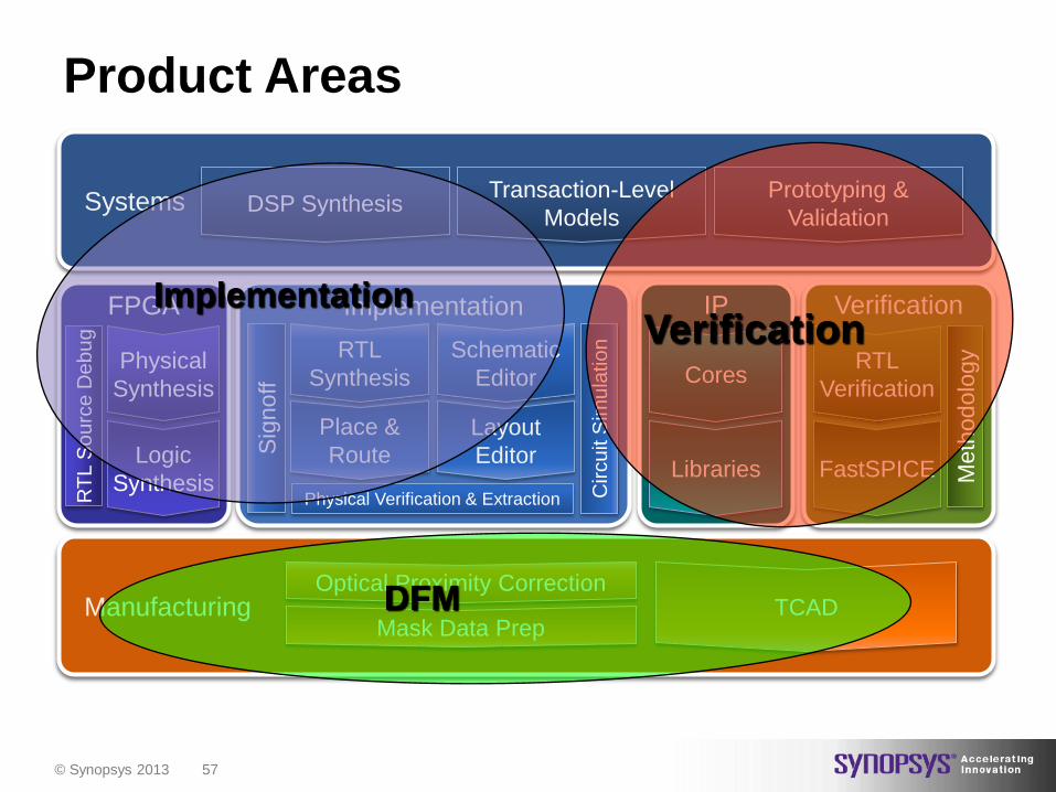
Product Areas
Manufacturing Mask Data Prep
Optical Proximity Correction TCAD
Verification
Meth
od
olo
gy
FastSPICE
RTL
Verification
IP
Libraries
Cores
FPGA
Logic
Synthesis
RT
L S
ou
rce
De
bu
g
Physical
Synthesis
Systems DSP Synthesis Transaction-Level
Models
Prototyping &
Validation
Implementation
Circu
it S
imu
latio
n
Physical Verification & Extraction
Place &
Route
RTL
Synthesis
Layout
Editor
Schematic
Editor
Sig
noff
Implementation Verification
DFM
© Synopsys 2013 58
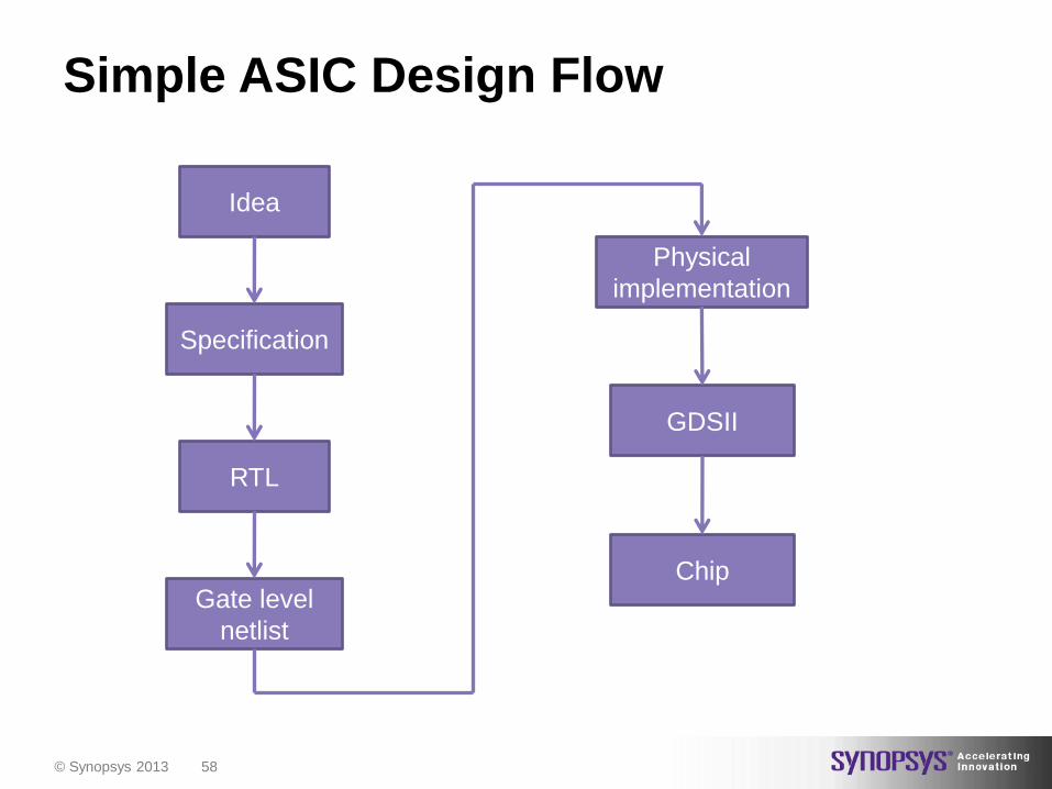
Simple ASIC Design Flow
Idea
Specification
RTL
Gate level
netlist
Physical
implementation
GDSII
Chip
© Synopsys 2013 59
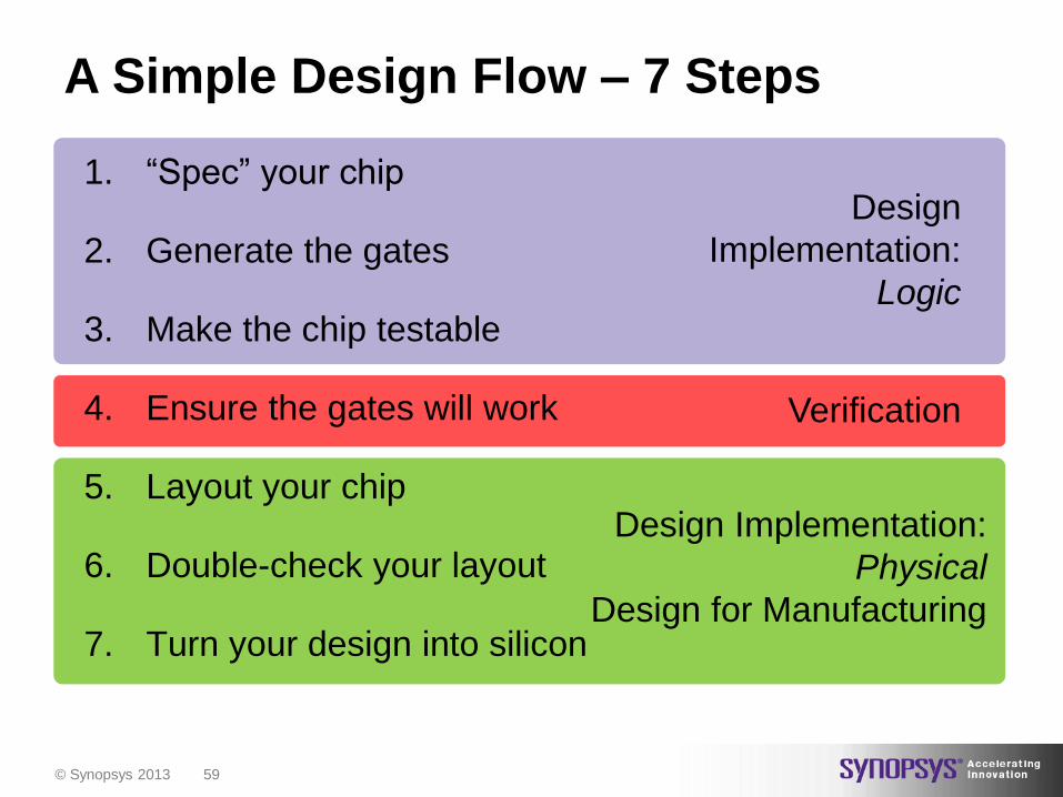
Design Implementation:
Physical
Design for Manufacturing
Verification
Design
Implementation:
Logic
1. “Spec” your chip
2. Generate the gates
3. Make the chip testable
4. Ensure the gates will work
5. Layout your chip
6. Double-check your layout
7. Turn your design into silicon
A Simple Design Flow – 7 Steps
© Synopsys 2013 60
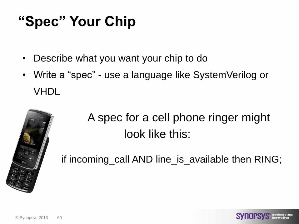
“Spec” Your Chip
• Describe what you want your chip to do
• Write a “spec” - use a language like SystemVerilog or
VHDL
A spec for a cell phone ringer might
look like this:
if incoming_call AND line_is_available then RING;
© Synopsys 2013 61
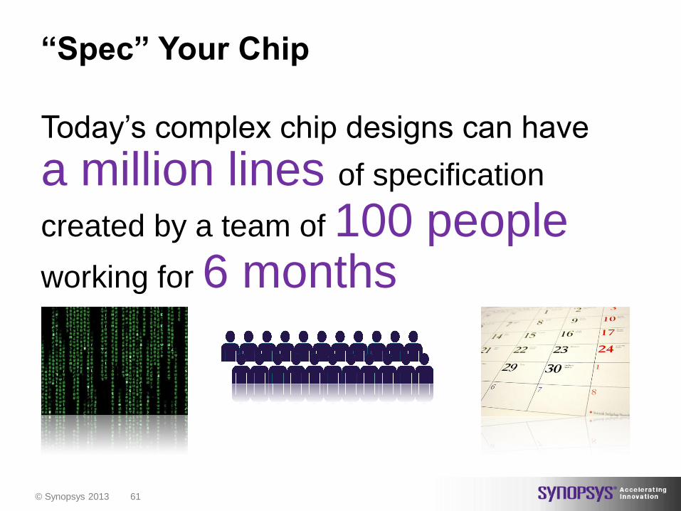
Today’s complex chip designs can have
a million lines of specification
created by a team of 100 people working for 6 months
“Spec” Your Chip
© Synopsys 2013 62
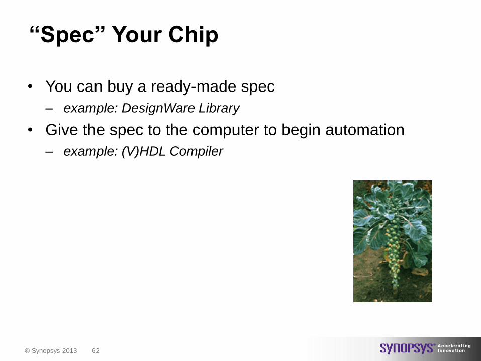
• You can buy a ready-made spec
– example: DesignWare Library
• Give the spec to the computer to begin automation
– example: (V)HDL Compiler
“Spec” Your Chip
© Synopsys 2013 63
• Goals and constraints of the design
• Functionality (what the chip will do)
• Performance (e.g speed and power)
• Technology constraints (e.g. size and space)
• Fabrication technology
Specification

© Synopsys 2013 64
• Decide the circuit architecture (structure)
– RISC/CISC
– ALU
– Pipelining
– Etc.
• Breaks the system into several sub systems
• Functionality of sub systems should match the
specification
• Sub systems need to be implemented through logic
representation (boolean expressions), FSM,
combinational logic, sequential logic, schematics, etc.
Logic Design
Structural and Functional Description
© Synopsys 2013 65
• Describes the several sub systems
• Should match the functional description
• Verilog or VHDL (Hardware description Language –
HDL)
• HDlL: Language used to describe a digital system
• Verification is performed at this stage to ensure that RTL
matches the idea
Register Transfer Level (RTL)
© Synopsys 2013 66
Generate the Gates
• Figure out the detailed logic
gates
• Use a computer program (EDA
tool)
• Synthesis
- example: Design Compiler,
Physical Compiler, IC Compiler
• Save the logic gates to use in
a future design
- example: DesignWare Library
© Synopsys 2013 67
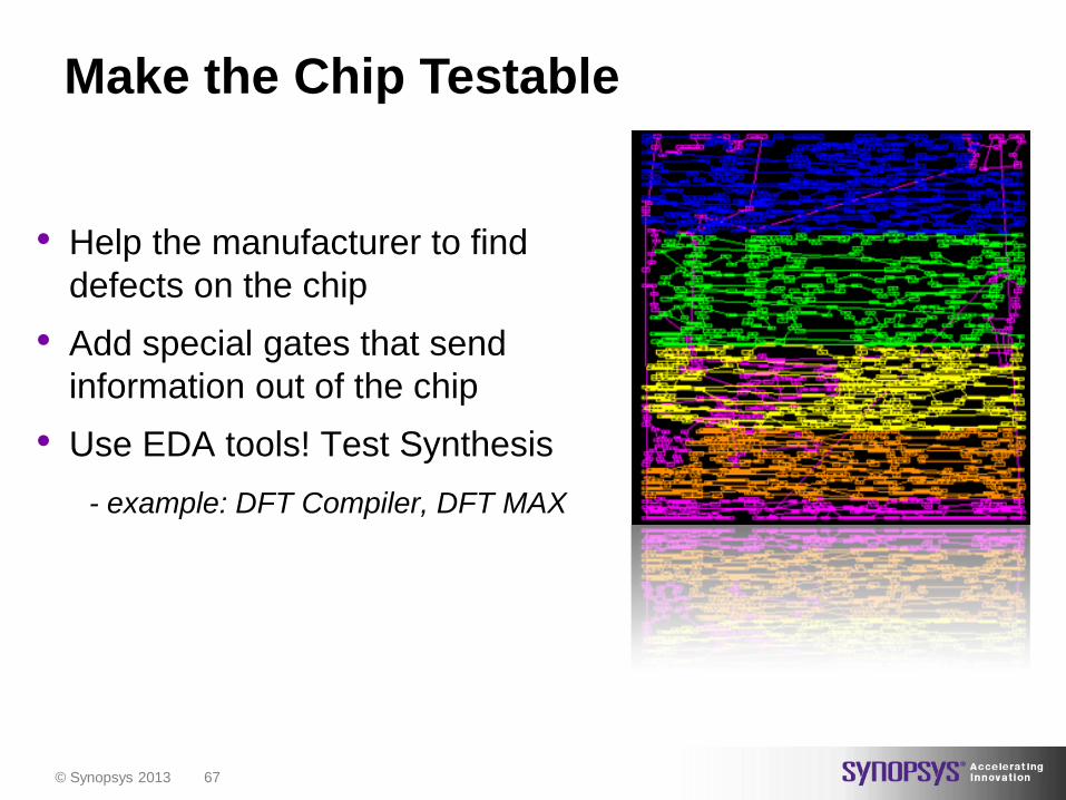
Make the Chip Testable
• Help the manufacturer to find
defects on the chip
• Add special gates that send
information out of the chip
• Use EDA tools! Test Synthesis
- example: DFT Compiler, DFT MAX
© Synopsys 2013 68
• Generated from the conversion of RTL into an optimized
gate level netlist
• Done by synthesis tools
• Synthesis tool takes an RTL description and a standard
cell library and produces a gate level netlist
• Considers constraints such as timing, area, testability,
and power
• The result is a completely structural description with only
standard cells at the leaves of the design
• This level is also verified by simulation or formal
verification
Gate Level Netlist
© Synopsys 2013 69
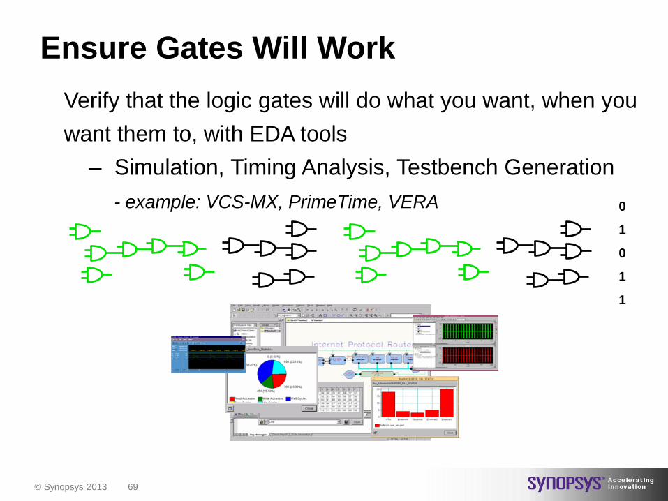
Ensure Gates Will Work
Verify that the logic gates will do what you want, when you
want them to, with EDA tools
– Simulation, Timing Analysis, Testbench Generation
- example: VCS-MX, PrimeTime, VERA 0
1
0
1
1

© Synopsys 2013 70
Ensure Gates Will Work
Put statements in the design description
– Assertion-based verification = “Smart Verification”
assert property (@(posedge clk) $rose(req)|-> ##[1:3] $rose(ack)); Assertion
always @(posedge req)
begin
repeat (1) @(posedge clk);
fork: pos_pos
begin
@(posedge ack)
$display("Assertion Success",$time);
disable pos_pos;
end
begin
repeat (2) @(posedge clk);
$display("Assertion Failure",$time);
disable pos_pos;
end
join
end // always
Old way
req
ack
0 1 2 3 4 5
Intended behavior
© Synopsys 2013 71
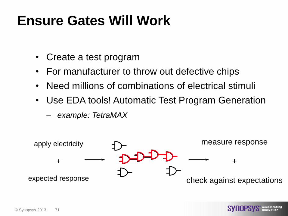
Ensure Gates Will Work
• Create a test program
• For manufacturer to throw out defective chips
• Need millions of combinations of electrical stimuli
• Use EDA tools! Automatic Test Program Generation
– example: TetraMAX
apply electricity
+
expected response
measure response
+
check against expectations
© Synopsys 2013 72
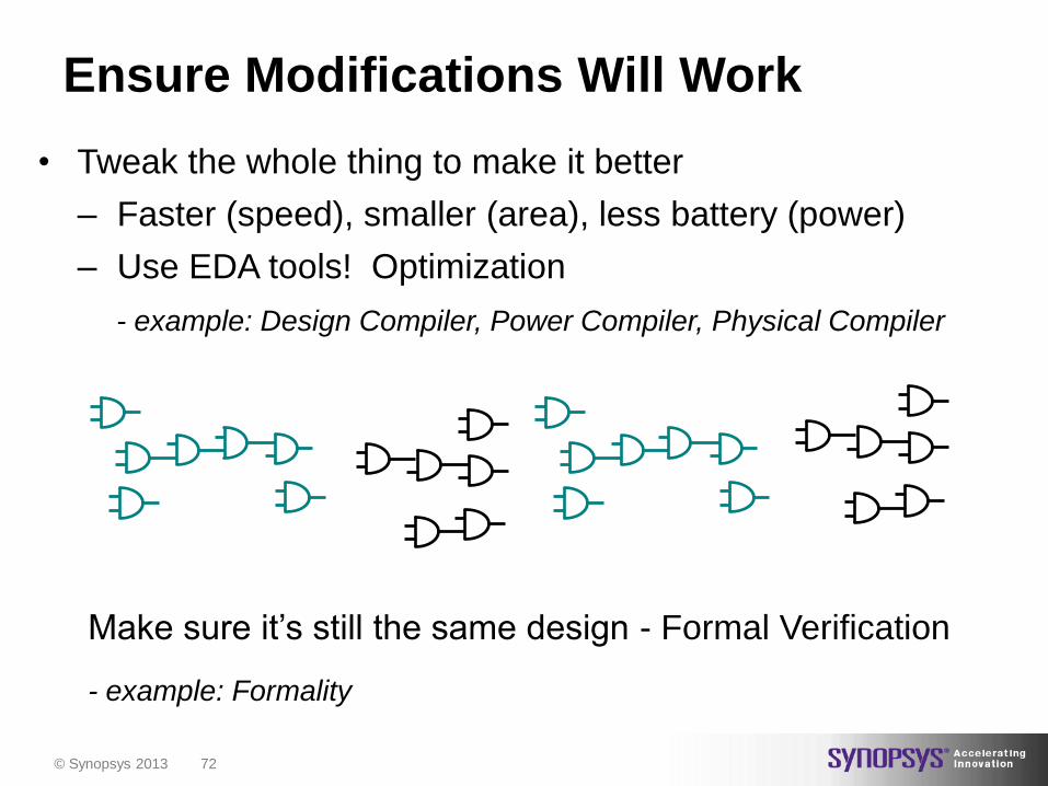
Ensure Modifications Will Work
• Tweak the whole thing to make it better
– Faster (speed), smaller (area), less battery (power)
– Use EDA tools! Optimization
- example: Design Compiler, Power Compiler, Physical Compiler
Make sure it’s still the same design - Formal Verification
- example: Formality

© Synopsys 2013 73
• Gate level netlist is converted into geometeric
representation
• It corresponds to the layout of the design
• Layout is designed according to design rules specified in
the library
• Consists in three sub steps
– Floor planning
– Placement
– Routing
• Produces a GDSII file
Physical Implementation

© Synopsys 2013 74
“Blueprint” Your Chip
• Design planning: create a “floorplan” so the gates will
go where you want
Floorplan
• Place the gates on a “blueprint” and route them
together (also called “layout ”)
• Show where the gates will be connected with wires
- example: Jupiter-XT, Physical Compiler, IC Compiler, Astro
© Synopsys 2013 75
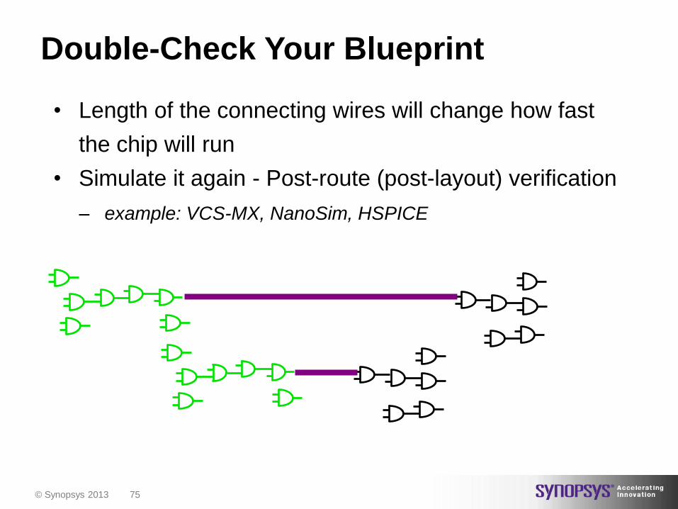
Double-Check Your Blueprint
• Length of the connecting wires will change how fast
the chip will run
• Simulate it again - Post-route (post-layout) verification
– example: VCS-MX, NanoSim, HSPICE
© Synopsys 2013 76
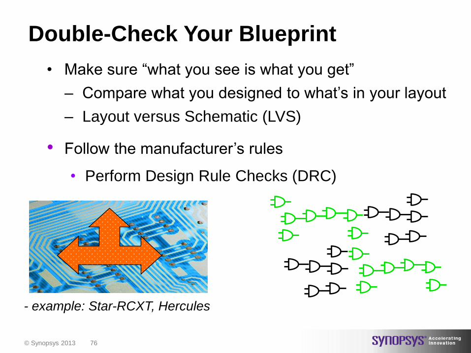
Double-Check Your Blueprint
• Make sure “what you see is what you get”
– Compare what you designed to what’s in your layout
– Layout versus Schematic (LVS)
• Follow the manufacturer’s rules
• Perform Design Rule Checks (DRC)
- example: Star-RCXT, Hercules
© Synopsys 2013 77
• File used by the foundry to fabricate the ASIC
• Physical verification is performed to verify if the layout is
designed according the rules
GDSII

© Synopsys 2013 78
Turn Your Design Into Sand
• Produce the layout data:
GDSII
- example: IC Compiler
© Synopsys 2013 79
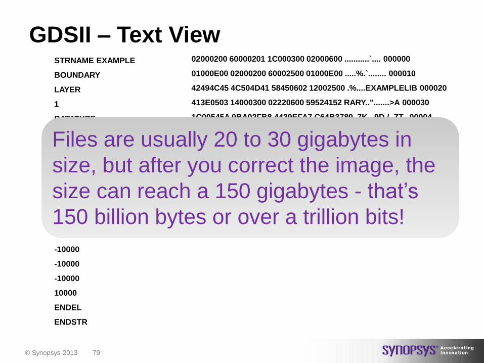
GDSII – Text View STRNAME EXAMPLE
BOUNDARY
LAYER
1
DATATYPE
0
XY
-10000
10000
20000
10000
20000
-10000
-10000
-10000
-10000
10000
ENDEL
ENDSTR
02000200 60000201 1C000300 02000600 ...........`.... 000000
01000E00 02000200 60002500 01000E00 .....%.`........ 000010
42494C45 4C504D41 58450602 12002500 .%....EXAMPLELIB 000020
413E0503 14000300 02220600 59524152 RARY..".......>A 000030
1C00545A 9BA02FB8 4439EFA7 C64B3789 .7K...9D./..ZT.. 00004
60000000 01000E00 02000200 60000205 ...`...........` 000050
58450606 0C001100 01000E00 02000200 ..............EX 000060
0100020D 06000008 04000045 4C504D41 AMPLE........... 000070
0000F0D8 FFFF0310 2C000000 020E0600 .......,........ 000080
FFFF204E 00001027 0000204E 00001027 '...N ..'...N .. 000090
0000F0D8 FFFFF0D8 FFFFF0D8 FFFFF0D8 ................ 0000A0
00000004 04000007 04000011 04001027 '............... 0000B0
00000000 00000000 00000000 00000000 ................ 0000C0
OR, Files are usually 20 to 30 gigabytes in
size, but after you correct the image, the
size can reach a 150 gigabytes - that’s
150 billion bytes or over a trillion bits!

© Synopsys 2013 80
Turn Your Design Into Sand
Correct the image
– example: Proteus, Progen, IC Workbench, SiVL/LRC, iN-
Phase, CATS
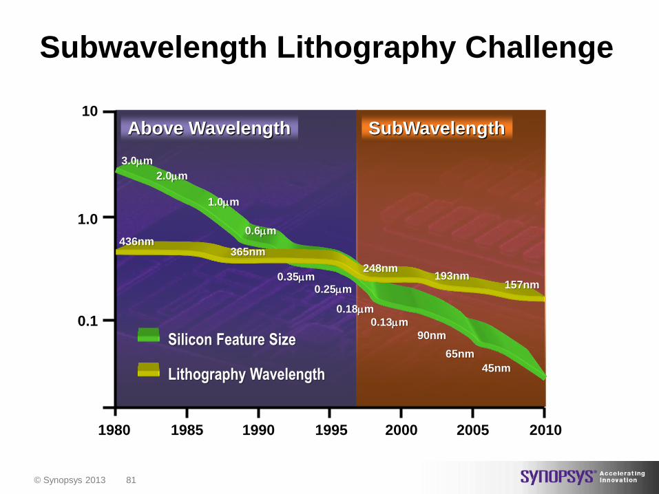
© Synopsys 2013 81
Above Wavelength SubWavelength
1980 1985 1990 1995 2000 2005 2010
0.1
1.0
10
Silicon Feature Size
3.0mm
2.0mm
1.0mm
0.6mm
0.35mm
45nm
65nm
90nm
0.13mm
0.18mm
0.25mm
Lithography Wavelength
436nm 365nm
248nm 193nm
157nm
Subwavelength Lithography Challenge
© Synopsys 2013 82
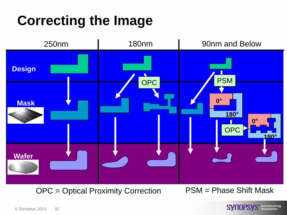
Correcting the Image
Design
Mask
Wafer
250nm 180nm
OPC
90nm and Below
PSM
0°
180°
OPC
0°
180°
OPC = Optical Proximity Correction PSM = Phase Shift Mask

© Synopsys 2013 83
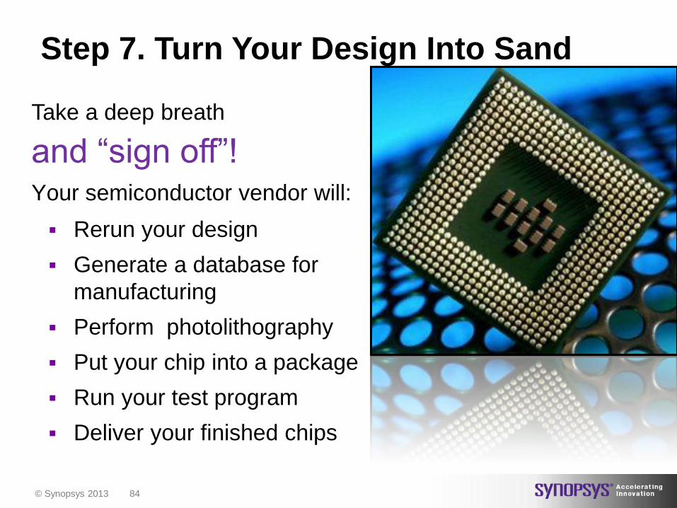
© Synopsys 2013 84
Your semiconductor vendor will:
Rerun your design
Generate a database for
manufacturing
Perform photolithography
Put your chip into a package
Run your test program
Deliver your finished chips
Take a deep breath
and “sign off”!
Step 7. Turn Your Design Into Sand
© Synopsys 2013 85
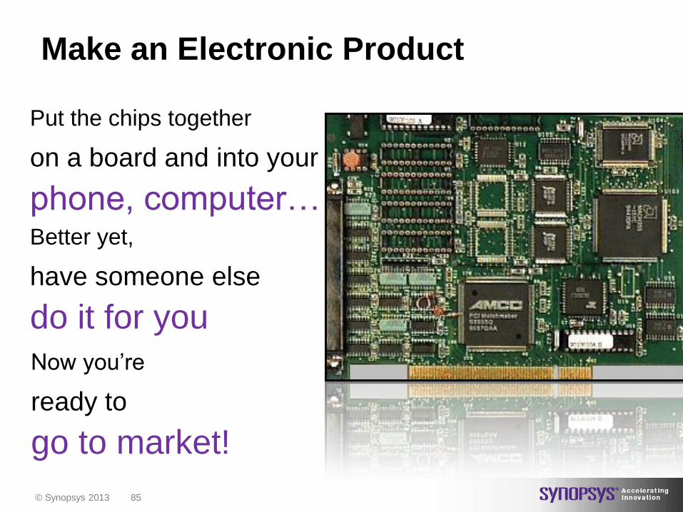
Put the chips together
on a board and into your
phone, computer… Better yet,
have someone else
do it for you
Make an Electronic Product
Now you’re
ready to
go to market!
© Synopsys 2013 86
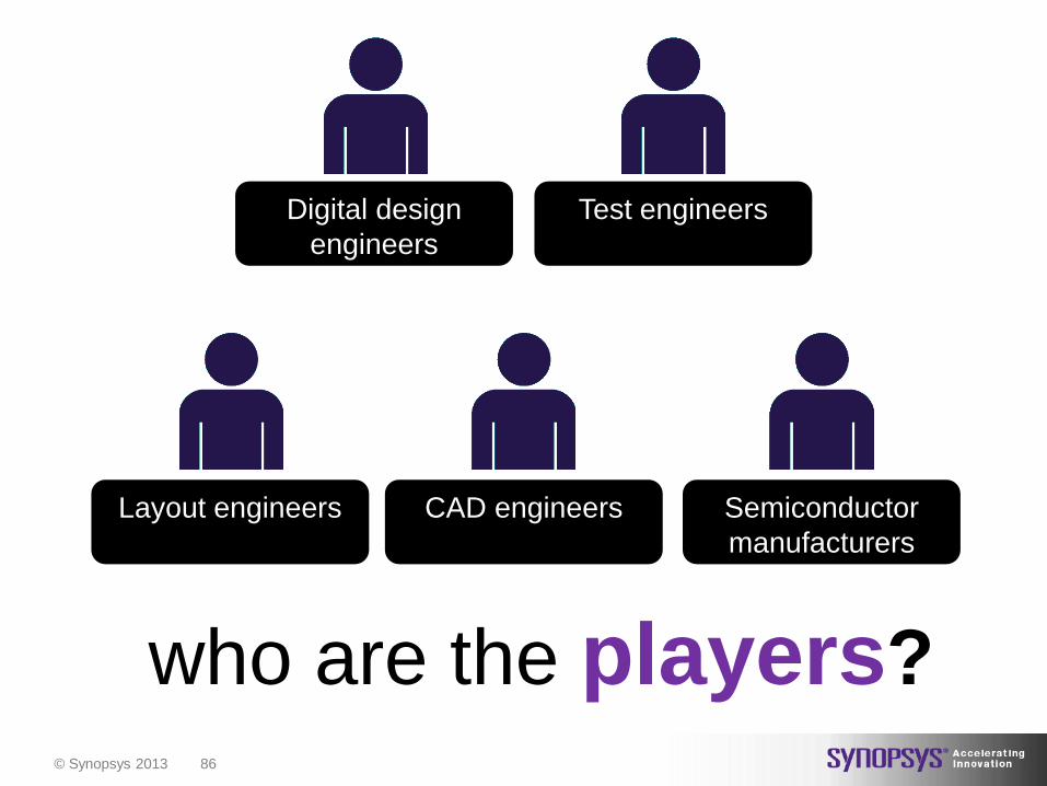
Layout engineers CAD engineers Semiconductor
manufacturers
Digital design
engineers
who are the players?
Test engineers

© Synopsys 2013 87
Best Practices
© Synopsys 2013 88
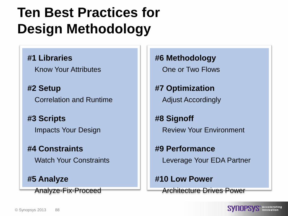
Ten Best Practices for
Design Methodology
#6 Methodology
One or Two Flows
#7 Optimization
Adjust Accordingly
#8 Signoff
Review Your Environment
#9 Performance
Leverage Your EDA Partner
#10 Low Power
Architecture Drives Power
#1 Libraries
Know Your Attributes
#2 Setup
Correlation and Runtime
#3 Scripts
Impacts Your Design
#4 Constraints
Watch Your Constraints
#5 Analyze
Analyze-Fix-Proceed

© Synopsys 2013 89
Why is my design larger in area?
Why is it taking so long to run?
#1 Libraries: Know Your Attributes
Watch for dont_use, dont_touch, and size_only usage in your
libraries and scripts
• Attributes are user-controlled to guide optimization
• Restricting optimization may lead to problems
After
Optimization
Original Area
New Area

© Synopsys 2013 90
• A properly designed set of library
cells give optimization engines more
choice
– Avoid cells sensitive to minor change
in load, impedes convergence
– Footprint-equivalent cells are useful
for final-stage optimization w/ minimal
perturbation to other design metrics
– Std. cell pins should be on grid -
(especially complex cells with small
drive strength: higher pin density)
– Multiple variants for each flop (drive
strengths, delays, setup times, .. )
• Library quality enabler for targeted
performance
Technology and IP Make Sure to Have a Good Quality Library
Example:
Cell Sensitivity To Load Uncertainty
De
lay
Cload C*
D
*
Cell A
Cell B
B
A
© Synopsys 2013 91
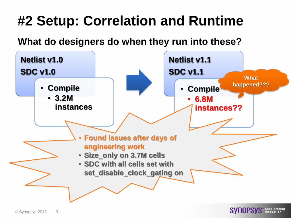
#2 Setup: Correlation and Runtime
Netlist v1.0
SDC v1.0
• Compile
• 3.2M instances
Netlist v1.1
SDC v1.1
• Compile
• 6.8M instances??
What
happened???
• Found issues after days of
engineering work
• Size_only on 3.7M cells
• SDC with all cells set with
set_disable_clock_gating on
What do designers do when they run into these?
© Synopsys 2013 92
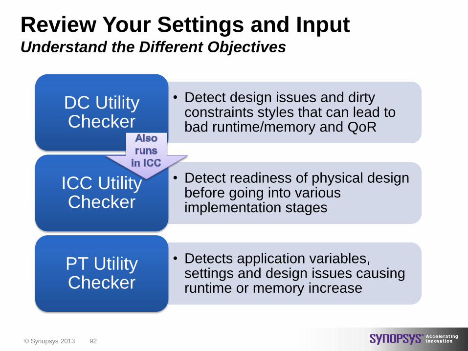
Review Your Settings and Input Understand the Different Objectives
• Detect design issues and dirty constraints styles that can lead to bad runtime/memory and QoR
DC Utility Checker
• Detect readiness of physical design before going into various implementation stages
ICC Utility Checker
• Detects application variables, settings and design issues causing runtime or memory increase
PT Utility Checker
© Synopsys 2013 93
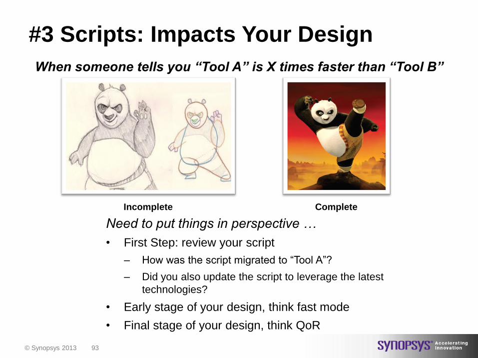
Need to put things in perspective …
• First Step: review your script
– How was the script migrated to “Tool A”?
– Did you also update the script to leverage the latest
technologies?
• Early stage of your design, think fast mode
• Final stage of your design, think QoR
#3 Scripts: Impacts Your Design
When someone tells you “Tool A” is X times faster than “Tool B”
Incomplete Complete
© Synopsys 2013 94
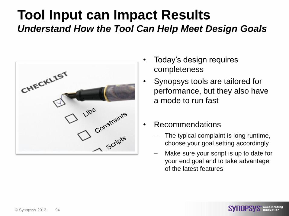
• Today’s design requires
completeness
• Synopsys tools are tailored for
performance, but they also have
a mode to run fast
• Recommendations
– The typical complaint is long runtime,
choose your goal setting accordingly
– Make sure your script is up to date for
your end goal and to take advantage
of the latest features
Tool Input can Impact Results Understand How the Tool Can Help Meet Design Goals
© Synopsys 2013 95
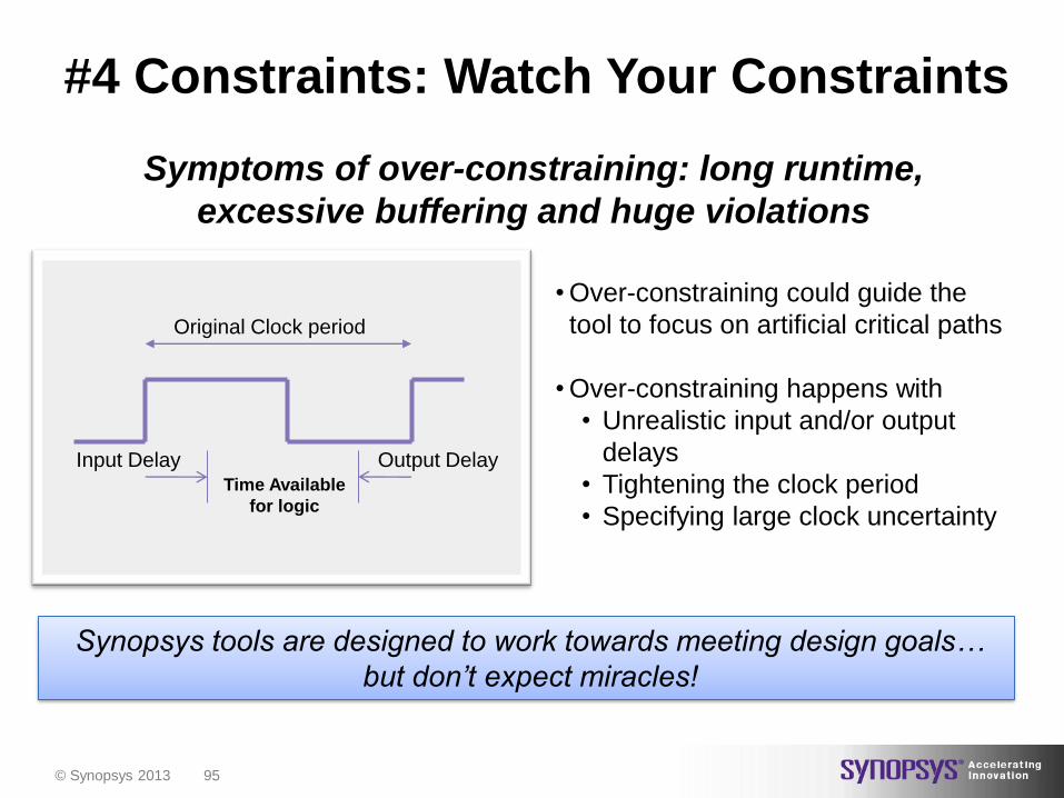
Symptoms of over-constraining: long runtime,
excessive buffering and huge violations
#4 Constraints: Watch Your Constraints
Original Clock period
Input Delay Output Delay Time Available
for logic
• Over-constraining could guide the
tool to focus on artificial critical paths
• Over-constraining happens with
• Unrealistic input and/or output
delays
• Tightening the clock period
• Specifying large clock uncertainty
Synopsys tools are designed to work towards meeting design goals…
but don’t expect miracles!

© Synopsys 2013 96
Understanding EDA Tool will help Simple Illustration
Circuit A Circuit B
Will DC do this transformation?
CLKA wns = -0.300
CLKB wns = -0.100
CLKA wns = -0.280
CLKB wns = -0.150
Default Weights Delay Cost Before Delay Cost After
CLKA weight = 1
CLKB weight = 1
0.30
0.10
0.28
0.15
Total WNS Cost 0.40 0.43
Adjusted Weights Delay Cost Before Delay Cost After
CLKA weight = 10
CLKB weight = 1
3.00
0.10
2.80
0.15
Total WNS Cost 3.10 2.95
Total cost increased
Transformation rejected
Worst WNS = -0.300
Total cost reduced
Transformation accepted
Worst WNS = -0.280
<
> √
Cost = ∑ pi * wi
© Synopsys 2013 97
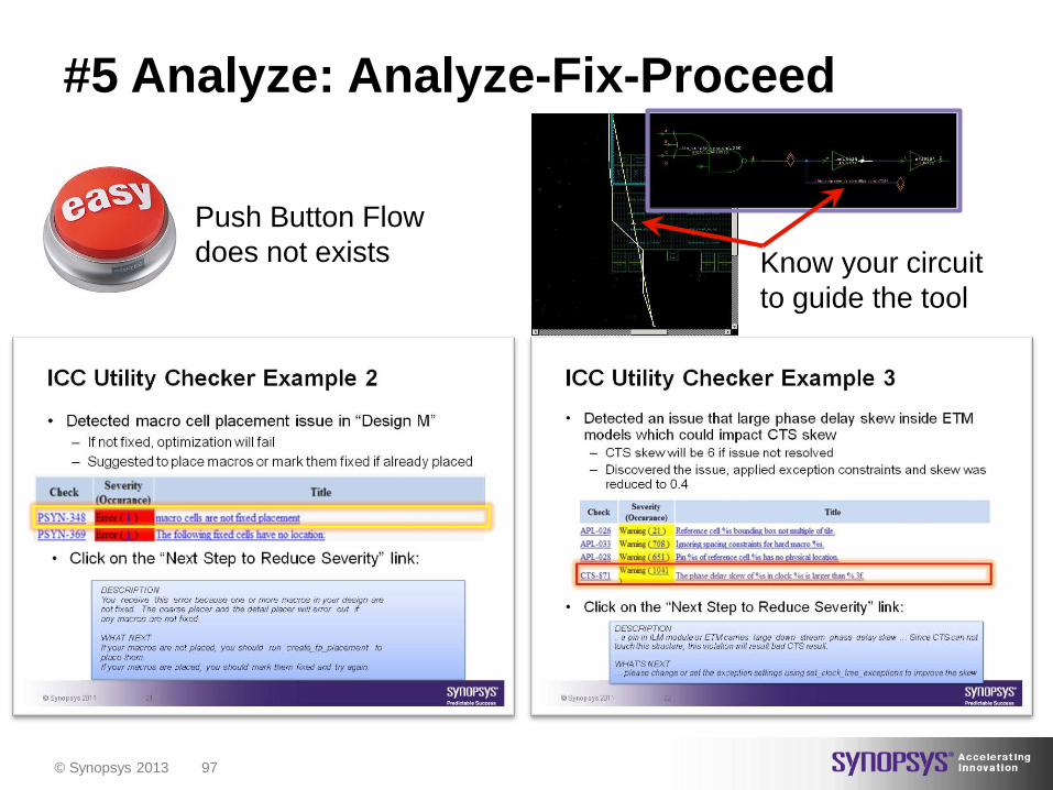
#5 Analyze: Analyze-Fix-Proceed
Push Button Flow
does not exists Know your circuit
to guide the tool
© Synopsys 2013 98
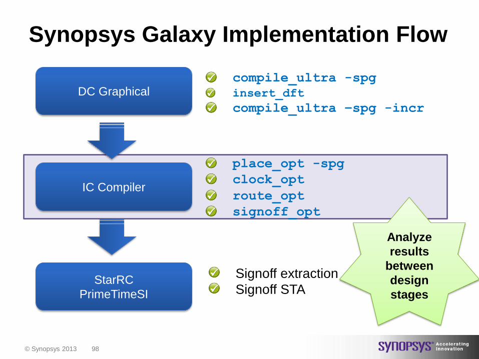
Synopsys Galaxy Implementation Flow
DC Graphical
IC Compiler
place_opt -spg
clock_opt
route_opt
signoff_opt
compile_ultra -spg
insert_dft
compile_ultra –spg -incr
StarRC
PrimeTimeSI
Signoff extraction
Signoff STA
Analyze
results
between
design
stages

© Synopsys 2013 99
Design specifications and constraints changes
constantly during the design cycle
#6 Methodology: One or Two Flows
180 nanometers (2000)
225K gates, 11 RAMs
150 MHz
45 nanometers (2010)
96mm2, ~ 300M transistors
7-9W
One flow
for both
exploration &
Implementation
Exploration flow
target for
early specs
& constraints
Implementation
flow
for final
design
realization
© Synopsys 2013 100
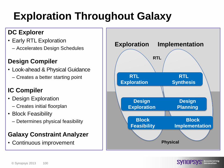
Exploration Throughout Galaxy
DC Explorer
• Early RTL Exploration
– Accelerates Design Schedules
Design Compiler
• Look-ahead & Physical Guidance
– Creates a better starting point
IC Compiler
• Design Exploration
– Creates initial floorplan
• Block Feasibility
– Determines physical feasibility
Galaxy Constraint Analyzer
• Continuous improvement
RTL
Exploration
RTL
Synthesis
Design
Exploration
Design
Planning
Block
Feasibility
Block
Implementation
Implementation Exploration
RTL
Physical
© Synopsys 2013 101
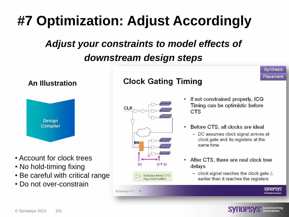
Adjust your constraints to model effects of
downstream design steps
#7 Optimization: Adjust Accordingly
Design
Compiler
• Account for clock trees
• No hold-timing fixing
• Be careful with critical range
• Do not over-constrain
An Illustration

© Synopsys 2013 102
• Synthesis and placement
– Do not over-constrain during synthesis
– Use DC SPG flow
– Account for max_transition and clock uncertainty
– Specify pre-CTS estimated constraints
• CTS
– Remove pre-CTS estimated constraints
• Route
– Remove/adjust pre-route constraints
– Adjust crosstalk thresholds
Manage Design Constraints Throughout Guidelines For Convergent Timing Closure
1029
971
913
800
850
900
950
1,000
1,050
1,100
Synthesis Place Clock Route
MH
z
Addnl. Customization For High-Performance
Tuned For Hi-Performance/Low Power
RM (Baseline)
Timing Closure Profile
Timing Closure
Profile
Do Not over
Complicate your flow

© Synopsys 2013 103
Runtime (CPU Hrs)
#8 Signoff: Review your Environment
0
16
32
48
64
80
96
112
128
1.1 1.2 5.5 37.0 50+
0
10
20
30
40
50
60
1.1 1.2 5.5 37.0 50+
Memory Usage (GB) 172 GB
Instances (Million) Instances (Million)
Designs run at customer site using revised
PrimeTime scripts and latest release version
Unlike wine, scripts grow stale with age
© Synopsys 2013 104
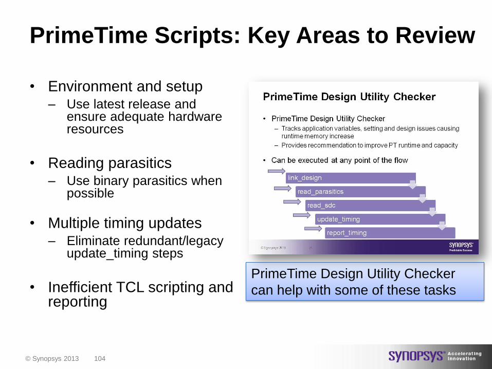
PrimeTime Scripts: Key Areas to Review
• Environment and setup – Use latest release and
ensure adequate hardware resources
• Reading parasitics – Use binary parasitics when
possible
• Multiple timing updates – Eliminate redundant/legacy
update_timing steps
• Inefficient TCL scripting and reporting
PrimeTime Design Utility Checker
can help with some of these tasks
© Synopsys 2013 105
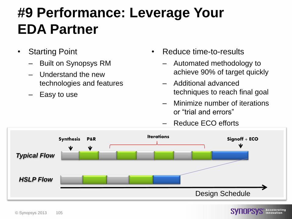
#9 Performance: Leverage Your
EDA Partner
• Starting Point
– Built on Synopsys RM
– Understand the new
technologies and features
– Easy to use
• Reduce time-to-results
– Automated methodology to
achieve 90% of target quickly
– Additional advanced
techniques to reach final goal
– Minimize number of iterations
or “trial and errors”
– Reduce ECO efforts
Synthesis
Design Schedule
Typical Flow
HSLP Flow
Signoff + ECO Iterations P&R
© Synopsys 2013 106
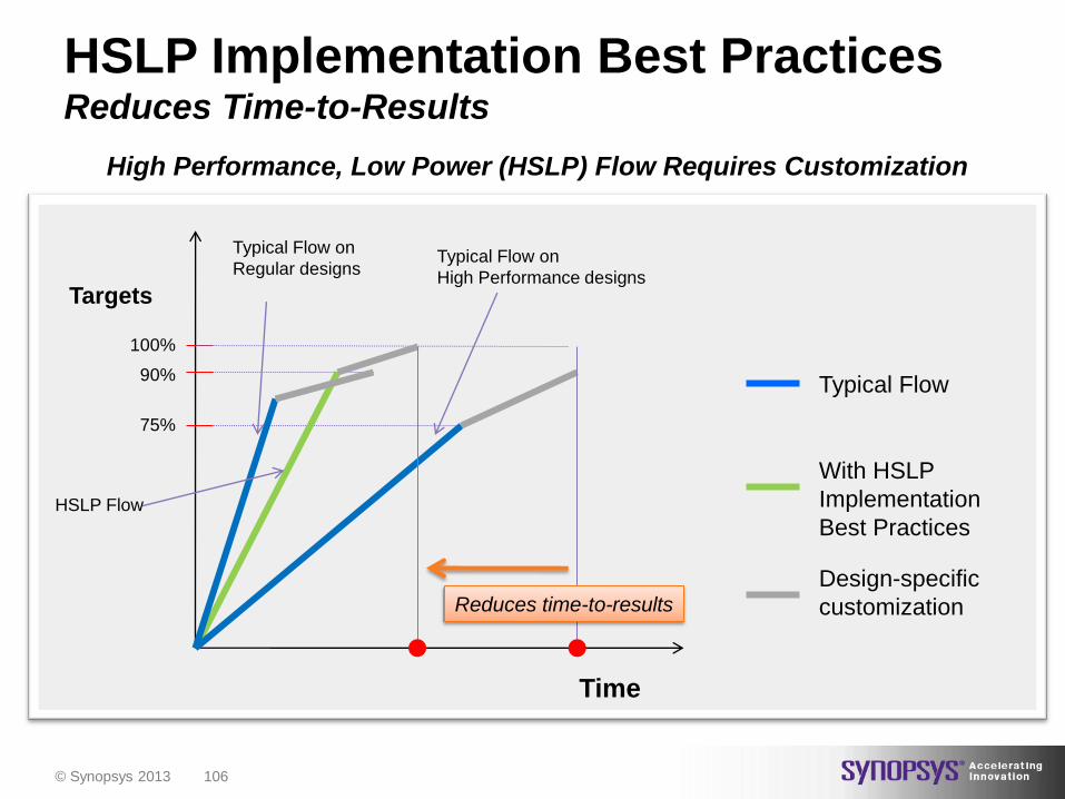
HSLP Implementation Best Practices Reduces Time-to-Results
Time
Targets
100%
90%
75%
Typical Flow
With HSLP
Implementation
Best Practices
Design-specific
customization Reduces time-to-results
Typical Flow on
Regular designs Typical Flow on
High Performance designs
HSLP Flow
High Performance, Low Power (HSLP) Flow Requires Customization
© Synopsys 2013 107
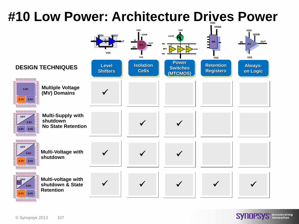
#10 Low Power: Architecture Drives Power
0.9V 0.7V
0.9V
OFF
0.9V 0.9V
0.9V
OFF
Multiple Voltage (MV) Domains
Multi-Supply with shutdown No State Retention
Multi-Voltage with shutdown
0.9V 0.7V
0.9V
0.9V 0.7V
0.9V
OFF
Multi-voltage with shutdown & State Retention
SR
Retention
Registers
Power
Switches
(MTCMOS)
Level
Shifters
Isolation
Cells
Always-
on Logic
DESIGN TECHNIQUES
VDDB
VSS
IN
OUT
EN
VDD
ISO
VSS
IN
VDDI VDDO
OUT L
S AO IN OUT
VDD
VDDB
VSS
Gate Gate
on/off
VDD
Gate
VSS
VDDB
VDD
RR
© Synopsys 2013 108
www.ieee-lascas.org
Santiago, Chile February 24 – 28 2014

© Synopsys 2013 109
Thank You


