
DIGITAL ALGORITHMS FOR ANALOG ADAPTIVE FILTERS
by
Anthony Chan Carusone
A thesis submitted in conformity with the requirementsfor the degree of Doctor of Philosophy
Graduate Department of Electrical and Computer EngineeringUniversity of Toronto
Copyright by Anthony Chan Carusone, 2002

ii
DIGITAL ALGORITHMS FOR ANALOG ADAPTIVE FILTERS
Anthony Chan Carusone
Degree of Doctor of PhilosophyGraduate Department of Electrical and Computer Engineering
University of Toronto2002
AbstractThe use of analog adaptive filters in modern integrated systems is limited by the com-
plexity of the analog adaptation hardware and by dc offset effects which limit the adapta-
tion accuracy. Both problems can be addressed by using an analog filter with a digital
adaptation algorithm.
The design of digitally programmable analog filters suitable for adaptive applications
is examined. Novel Gm-C circuits are described and implemented in a CMOS prototype
5th order integrated filter with digitally programmable poles and zeros. However, the
greatest challenge associated with performing digital adaptation of an analog filter is
obtaining the gradient information without overcomplicating the analog design. Three
main approaches to overcoming this challenge are described. First, the gradient informa-
tion is obtained by correlating changes in the output squared error to independent dither
on the adapted parameters. Second, the internal state signals (and, hence, the gradient
signals) are calculated from a time delayed input vector using a co-ordinate transforma-
tion. Third, time delayed estimates of the filter input are obtained digitally from the filter
output and used to calculate the required gradient signals. All three techniques use digital

iii
signal processing to obtain the gradient information and require little, if any, additional
analog hardware. The performance of the new adaptive algorithms are discussed and
several variations are proposed to simplify integrated implementations. The prototype
integrated analog filter was used as a testbed to verify two of the novel algorithms. Gra-
dient descent optimization of analog filter parameters was successfully performed with-
out access to any of the filter’s internal state signals, which was not previously possible.
As a result, designers of analog adaptive filters are now free to perform the filter design
without being restricted by the requirements of the adaptation algorithm.

iv
Acknowledgements
First and foremost, I would like to thank my supervisor and friend Prof. David A.
Johns for providing an interesting project, constant direction, valuable advice, and most
of all, for providing me with opportunity. He has my appreciation and tremendous
respect.
Thanks, also, to my supervisory committee, Prof. Ken Martin and Prof. Bruce A.
Francis, and to the external examiner Dr. Ayal Shoval for their time and effort. Their
efforts have substantially improved the quality of this thesis.
Thanks to all of my peers in the electronics research group. It is not without consid-
erable regret that I refrain from attempting to list them all; however, there have been so
many people who have contributed in so many different ways that a list somehow seems
inappropriate. I would also like to gratefully acknowledge the support of NSERC, CMC,
and Micronet.
Great personal thanks goes to my family and friends who have provided me with
much needed and appreciated support and guidance. Finally, I would like to thank my
wife, Soo. She is my partner in everything, and this dissertation is no exception.

v
Contents
Abstract ii
Acknowledgements iv
Contents v
List of Tables viii
List of Figures ix
List of Abbreviations xiv
Chapter 1: Introduction 11.1 Motivation. . . . . . . . . . . . . . . . . . . . . . . . . . . . . . . . . . . . . . . . . . . . . . . . . . .11.2 Applications and the State of the Art. . . . . . . . . . . . . . . . . . . . . . . . . . . . .2
1.2.1 Digital Magnetic Storage . . . . . . . . . . . . . . . . . . . . . . . . . . . . . . . . . . . . . 21.2.2 Ethernet Over Copper . . . . . . . . . . . . . . . . . . . . . . . . . . . . . . . . . . . . . . 51.2.3 High Speed Serial Links . . . . . . . . . . . . . . . . . . . . . . . . . . . . . . . . . . . . . 61.2.4 Optical and Wireless . . . . . . . . . . . . . . . . . . . . . . . . . . . . . . . . . . . . . . . . 7
1.3 Background . . . . . . . . . . . . . . . . . . . . . . . . . . . . . . . . . . . . . . . . . . . . . . . . .71.3.1 The Least Mean-Square (LMS) Algorithm. . . . . . . . . . . . . . . . . . . . . . . 81.3.2 DC Offset Effects in Analog LMS. . . . . . . . . . . . . . . . . . . . . . . . . . . . . 9
1.4 Outline. . . . . . . . . . . . . . . . . . . . . . . . . . . . . . . . . . . . . . . . . . . . . . . . . . . . .111.5 References. . . . . . . . . . . . . . . . . . . . . . . . . . . . . . . . . . . . . . . . . . . . . . . . . .12
Chapter 2: Digitally Programmable Gm-C Filters 172.1 Introduction . . . . . . . . . . . . . . . . . . . . . . . . . . . . . . . . . . . . . . . . . . . . . . . .172.2 Circuit Description . . . . . . . . . . . . . . . . . . . . . . . . . . . . . . . . . . . . . . . . . .19
2.2.1 A CMOS Transconductor . . . . . . . . . . . . . . . . . . . . . . . . . . . . . . . . . . 192.2.2 Digitally Programmable Gain . . . . . . . . . . . . . . . . . . . . . . . . . . . . . . . . 202.2.3 Miller Integrator . . . . . . . . . . . . . . . . . . . . . . . . . . . . . . . . . . . . . . . . . . 212.2.4 Common Mode Feedback . . . . . . . . . . . . . . . . . . . . . . . . . . . . . . . . . . 232.2.5 Prototype . . . . . . . . . . . . . . . . . . . . . . . . . . . . . . . . . . . . . . . . . . . . . . . . 26
2.3 Experimental Measurements . . . . . . . . . . . . . . . . . . . . . . . . . . . . . . . . . .282.3.1 Programmable Transconductors . . . . . . . . . . . . . . . . . . . . . . . . . . . . . 282.3.2 Frequency Response . . . . . . . . . . . . . . . . . . . . . . . . . . . . . . . . . . . . . . . 282.3.3 Linearity . . . . . . . . . . . . . . . . . . . . . . . . . . . . . . . . . . . . . . . . . . . . . . . . . 312.3.4 Noise . . . . . . . . . . . . . . . . . . . . . . . . . . . . . . . . . . . . . . . . . . . . . . . . . . . 35

vi
2.3.5 Spurious-Free Dynamic Range . . . . . . . . . . . . . . . . . . . . . . . . . . . . . . . 362.4 Fine Tuning the Transconductances . . . . . . . . . . . . . . . . . . . . . . . . . . . .37
2.4.1 4-Bit Vcntrl DAC . . . . . . . . . . . . . . . . . . . . . . . . . . . . . . . . . . . . . . . . . 382.4.2 Hysteresis. . . . . . . . . . . . . . . . . . . . . . . . . . . . . . . . . . . . . . . . . . . . . . . . 402.4.3 Results . . . . . . . . . . . . . . . . . . . . . . . . . . . . . . . . . . . . . . . . . . . . . . . . . . 41
2.5 Power Consumption . . . . . . . . . . . . . . . . . . . . . . . . . . . . . . . . . . . . . . . . .432.6 Conclusions. . . . . . . . . . . . . . . . . . . . . . . . . . . . . . . . . . . . . . . . . . . . . . . . .442.7 Appendix - Derivation of Eqn. (2.1) . . . . . . . . . . . . . . . . . . . . . . . . . . . . .462.8 Appendix - Digital Circuitry. . . . . . . . . . . . . . . . . . . . . . . . . . . . . . . . . . .482.9 References. . . . . . . . . . . . . . . . . . . . . . . . . . . . . . . . . . . . . . . . . . . . . . . . . .49
Chapter 3: The Dithered Linear Search Algorithm 523.1 Introduction . . . . . . . . . . . . . . . . . . . . . . . . . . . . . . . . . . . . . . . . . . . . . . . .523.2 Background . . . . . . . . . . . . . . . . . . . . . . . . . . . . . . . . . . . . . . . . . . . . . . . .53
3.2.1 The Least Mean Square (LMS) Algorithm. . . . . . . . . . . . . . . . . . . . . . 543.2.2 The Differential Steepest Descent Algorithm . . . . . . . . . . . . . . . . . . . 54
3.3 The Dithered Linear Search . . . . . . . . . . . . . . . . . . . . . . . . . . . . . . . . . . .553.3.1 The Block DLS Algorithm . . . . . . . . . . . . . . . . . . . . . . . . . . . . . . . . . . 56
3.4 Theoretical Analysis . . . . . . . . . . . . . . . . . . . . . . . . . . . . . . . . . . . . . . . . .573.4.1 Preliminaries . . . . . . . . . . . . . . . . . . . . . . . . . . . . . . . . . . . . . . . . . . . . . 573.4.2 Convergence . . . . . . . . . . . . . . . . . . . . . . . . . . . . . . . . . . . . . . . . . . . . . 583.4.3 Perturbation. . . . . . . . . . . . . . . . . . . . . . . . . . . . . . . . . . . . . . . . . . . . . . 613.4.4 Noise in the Gradient Estimates . . . . . . . . . . . . . . . . . . . . . . . . . . . . . 623.4.5 Misadjustment . . . . . . . . . . . . . . . . . . . . . . . . . . . . . . . . . . . . . . . . . . . . 653.4.6 Total Excess MSE. . . . . . . . . . . . . . . . . . . . . . . . . . . . . . . . . . . . . . . . . 653.4.7 Comparison of the LMS, DSD, and DLS Algorithms . . . . . . . . . . . . 66
3.5 Behavioral Simulations . . . . . . . . . . . . . . . . . . . . . . . . . . . . . . . . . . . . . . .683.5.1 5-Tap FIR Filter . . . . . . . . . . . . . . . . . . . . . . . . . . . . . . . . . . . . . . . . . . 683.5.2 3rd Order Continuous Time Orthonormal Ladder Filter . . . . . . . . . . 69
3.6 Different Dither Signals. . . . . . . . . . . . . . . . . . . . . . . . . . . . . . . . . . . . . . .713.7 Dc Offset Effects. . . . . . . . . . . . . . . . . . . . . . . . . . . . . . . . . . . . . . . . . . . . .753.8 Subsampling . . . . . . . . . . . . . . . . . . . . . . . . . . . . . . . . . . . . . . . . . . . . . . . .783.9 Quantization. . . . . . . . . . . . . . . . . . . . . . . . . . . . . . . . . . . . . . . . . . . . . . . .803.10 Experimental Results. . . . . . . . . . . . . . . . . . . . . . . . . . . . . . . . . . . . . . . . .81
3.10.1 1st Order Lowpass Filter . . . . . . . . . . . . . . . . . . . . . . . . . . . . . . . . . . . 823.10.2 5th Order Orthonormal Ladder Filter . . . . . . . . . . . . . . . . . . . . . . . . . 85
3.11 Conclusions. . . . . . . . . . . . . . . . . . . . . . . . . . . . . . . . . . . . . . . . . . . . . . . . .873.12 Appendix - Proof of Eqn. (3.30) . . . . . . . . . . . . . . . . . . . . . . . . . . . . . . . .893.13 References. . . . . . . . . . . . . . . . . . . . . . . . . . . . . . . . . . . . . . . . . . . . . . . . . .91

vii
Chapter 4: Filter Adaptation Using Co-OrdinateTransformations 92
4.1 Introduction . . . . . . . . . . . . . . . . . . . . . . . . . . . . . . . . . . . . . . . . . . . . . . . .924.2 FIR Filter Adaptation Using Co-Ordinate Transformations . . . . . . . .93
4.2.1 The LMS Algorithm with a Co-ordinate Transform. . . . . . . . . . . . . . 934.2.2 The LMS Algorithm with an Inverse Co-ordinate Transform . . . . . . 95
4.3 Convergence and Misadjustment Analysis . . . . . . . . . . . . . . . . . . . . . . .974.4 Extension to IIR and Continuous Time Filters . . . . . . . . . . . . . . . . . . . .994.5 Simulation Results . . . . . . . . . . . . . . . . . . . . . . . . . . . . . . . . . . . . . . . . . .101
4.5.1 Orthonormal Ladder Filter . . . . . . . . . . . . . . . . . . . . . . . . . . . . . . . . . 1014.5.2 Feed Forward Companion Form Filter . . . . . . . . . . . . . . . . . . . . . . . 105
4.6 Hardware Implementation Issues . . . . . . . . . . . . . . . . . . . . . . . . . . . . .1084.6.1 Signed Algorithms . . . . . . . . . . . . . . . . . . . . . . . . . . . . . . . . . . . . . . . . 1094.6.2 Subsampling. . . . . . . . . . . . . . . . . . . . . . . . . . . . . . . . . . . . . . . . . . . . . 110
4.6.2.1 Subsampling an LMS transversal filter . . . . . . . . . . . . . . . . 1124.6.2.2 Extension to adaptive linear combiners . . . . . . . . . . . . . . . 115
4.7 Experimental Results. . . . . . . . . . . . . . . . . . . . . . . . . . . . . . . . . . . . . . . .1164.8 Conclusions. . . . . . . . . . . . . . . . . . . . . . . . . . . . . . . . . . . . . . . . . . . . . . . .1204.9 References. . . . . . . . . . . . . . . . . . . . . . . . . . . . . . . . . . . . . . . . . . . . . . . . .122
Chapter 5: Obtaining Gradient Signals by UnknownInput State Observation 124
5.1 Introduction . . . . . . . . . . . . . . . . . . . . . . . . . . . . . . . . . . . . . . . . . . . . . . .1245.2 Unknown Input Observation . . . . . . . . . . . . . . . . . . . . . . . . . . . . . . . . .1255.3 Approximate Time Delayed State Observation . . . . . . . . . . . . . . . . . .126
5.3.1 Background . . . . . . . . . . . . . . . . . . . . . . . . . . . . . . . . . . . . . . . . . . . . . 1265.3.2 Derivation of the Approximate Inverse Filter . . . . . . . . . . . . . . . . . . 1285.3.3 Approximation Error . . . . . . . . . . . . . . . . . . . . . . . . . . . . . . . . . . . . . 1295.3.4 Transmission Zeros in the Adapted Filter . . . . . . . . . . . . . . . . . . . . . 131
5.4 Simulation Results . . . . . . . . . . . . . . . . . . . . . . . . . . . . . . . . . . . . . . . . . .1315.4.1 2-Tap Transversal Filter . . . . . . . . . . . . . . . . . . . . . . . . . . . . . . . . . . . 1335.4.2 Effect of Mismatches . . . . . . . . . . . . . . . . . . . . . . . . . . . . . . . . . . . . . 1375.4.3 Dc Offset Effects . . . . . . . . . . . . . . . . . . . . . . . . . . . . . . . . . . . . . . . . 1395.4.4 5th Order Continuous Time Filter . . . . . . . . . . . . . . . . . . . . . . . . . . . 139
5.5 Hardware Requirements. . . . . . . . . . . . . . . . . . . . . . . . . . . . . . . . . . . . .1405.6 Conclusions. . . . . . . . . . . . . . . . . . . . . . . . . . . . . . . . . . . . . . . . . . . . . . . .1425.7 References. . . . . . . . . . . . . . . . . . . . . . . . . . . . . . . . . . . . . . . . . . . . . . . . .143
Chapter 6: Conclusion 1456.1 Summary. . . . . . . . . . . . . . . . . . . . . . . . . . . . . . . . . . . . . . . . . . . . . . . . . .1456.2 Future Work. . . . . . . . . . . . . . . . . . . . . . . . . . . . . . . . . . . . . . . . . . . . . . .1466.3 References. . . . . . . . . . . . . . . . . . . . . . . . . . . . . . . . . . . . . . . . . . . . . . . . .148

viii
List of Tables
Table 2.1 Summary of prototype filter IC measurements. . . . . . . . . . . . . . . . . . . .45Table 2.2 Digital register file address map. . . . . . . . . . . . . . . . . . . . . . . . . . . . . . . .49Table 3.1 Performance measures for gradient descent adaptive algorithms. . . . . .67Table 3.2 Summary of adaptive algorithms for the 5-tap transversal filter simula-
tions. . . . . . . . . . . . . . . . . . . . . . . . . . . . . . . . . . . . . . . . . . . . . . . . . . . . . .69Table 3.3 Summary of adaptive algorithm simulations for the 3rd order orthonormal
ladder filter. . . . . . . . . . . . . . . . . . . . . . . . . . . . . . . . . . . . . . . . . . . . . . . . .71Table 3.4 Comparison of relative excess MSE in steady state observed in simulations
using different algorithms and dither signals. . . . . . . . . . . . . . . . . . . . . .77Table 6.1 Comparison of digital algorithms for analog adaptive filters. . . . . . . .146

ix
List of Figures
Figure 1.1 System architectures for digital magnetic recording read channels. . . . . .3Figure 1.2 Adaptive echo cancellation in a full-duplex wired digital communication
transceiver: (A) digital, (B) mixed signal, (C) analog. . . . . . . . . . . . . . . . .6Figure 1.3 An LMS analog adaptive filter as a 2-input, 2-output system. . . . . . . . . .8Figure 1.4 Analog implementation of the LMS parameter update equation. . . . . .10Figure 1.5 DC tap for adaptive offset cancellation. . . . . . . . . . . . . . . . . . . . . . . . . .10Figure 1.6 Median-based DC offset compensation scheme. . . . . . . . . . . . . . . . . . .11Figure 2.1 Three transconductors based upon triode-region MOS devices (M3). .20Figure 2.2 A five-bit programmable triode conductance. . . . . . . . . . . . . . . . . . . . .21Figure 2.4 Differential integrators: (A) Gm-C (B) Gm-Opamp-C. . . . . . . . . . . . . .22Figure 2.3 Digital control of the output current mirror gain. . . . . . . . . . . . . . . . . .22Figure 2.5 Current input CMOS active integrators. . . . . . . . . . . . . . . . . . . . . . . . . .23Figure 2.6 Block diagram of the continuous time CMFB circuit. . . . . . . . . . . . . . .24Figure 2.7 Schematic diagram of the continuous time CMFB. . . . . . . . . . . . . . . . .24Figure 2.8 CMFB loop block diagram. . . . . . . . . . . . . . . . . . . . . . . . . . . . . . . . . . . .25Figure 2.9 Redesigned CMFB loop block diagram. . . . . . . . . . . . . . . . . . . . . . . . . .25Figure 2.10 Redesigned Miller integrator to reduce common mode loop gain. . . . .26Figure 2.11 5th order orthonormal ladder filter structure with multiple feed-ins. . .27Figure 2.12 Die photo of the prototype. . . . . . . . . . . . . . . . . . . . . . . . . . . . . . . . . . . .27Figure 2.13 First order Gm-C filter with programmable pole and dc gain. . . . . . . .27Figure 2.14 Gain of the first order filter as a function of the Gm1 control word. . .29Figure 2.15 Test setup used to isolate the frequency response of the filter. . . . . . . .30Figure 2.16 Magnitude response of the reference filter path, Href(s). . . . . . . . . . . . .30Figure 2.17 Measured frequency responses of the orthonormal ladder. . . . . . . . . . .31Figure 2.18 Measured frequency response of the lowpass orthonormal ladder showing
ringing around 500 MHz. . . . . . . . . . . . . . . . . . . . . . . . . . . . . . . . . . . . . .31Figure 2.20 Output spectrum of the 1st order filter with an input tone at 8 MHz. .32Figure 2.19 Simulated magnitude response of the 5th order lowpass filter. . . . . . . .32Figure 2.21 Spectrum analyzer screen shot of the 5th order filter output THD. . . .33Figure 2.22 THD of the 5th order lowpass filter vs. output amplitude. . . . . . . . . . .33Figure 2.23 THD of 5th order lowpass filter vs. input frequency. . . . . . . . . . . . . . .34Figure 2.24 Linearity simulations of the 5th order lowpass filter. . . . . . . . . . . . . . . .35

x
Figure 2.25 Noise spectrum of (A) the reference and (B) the signal paths. . . . . . . .36Figure 2.26 Total harmonic distortion power of the 5th order filter referenced to the
filter output. . . . . . . . . . . . . . . . . . . . . . . . . . . . . . . . . . . . . . . . . . . . . . . .37Figure 2.27 Using a four-bit DAC to program the gate control voltage, Vcntrl. . . .38Figure 2.29 A systematic offset error in the CMFB. . . . . . . . . . . . . . . . . . . . . . . . . .39Figure 2.28 Details of the 4-bit DAC. . . . . . . . . . . . . . . . . . . . . . . . . . . . . . . . . . . . . .39Figure 2.30 Implementation of DAC current sources in terms of unit current
sources. . . . . . . . . . . . . . . . . . . . . . . . . . . . . . . . . . . . . . . . . . . . . . . . . . . .40Figure 2.31 Probed DAC output voltage vs. 4-bit input word for different coarse con-
trol words. . . . . . . . . . . . . . . . . . . . . . . . . . . . . . . . . . . . . . . . . . . . . . . . . .41Figure 2.32 Normalized gain of the 1st order test structure vs. 4-bit input word for dif-
ferent coarse control words. . . . . . . . . . . . . . . . . . . . . . . . . . . . . . . . . . . .41Figure 2.33 Simulation results of the DAC subcircuit. . . . . . . . . . . . . . . . . . . . . . . . .42Figure 2.34 Current consumption of the prototype IC by functional block. . . . . . .43Figure 2.35 Small-signal equivalent half-circuit of the transconductor. . . . . . . . . . .47Figure 2.36 Sample timing diagram for serial digital interface. . . . . . . . . . . . . . . . . .49Figure 2.37 Schematic diagram for a 4-pin digital serial interface. . . . . . . . . . . . . . . .50Figure 3.1 Block diagram of the dithered linear search algorithm. . . . . . . . . . . . . .57Figure 3.2 Perturbation in a 2-dimensional parameter space using (A) the DSD algo-
rithm (B) the DLS algorithm. . . . . . . . . . . . . . . . . . . . . . . . . . . . . . . . . . .63Figure 3.3 Model matching simulations block diagram. . . . . . . . . . . . . . . . . . . . . . .68Figure 3.4 Simulation results for a 5-tap adaptive transversal filter. . . . . . . . . . . . .70Figure 3.5 A 3rd order orthonormal ladder filter using multiple feed-ins of the input
signal. . . . . . . . . . . . . . . . . . . . . . . . . . . . . . . . . . . . . . . . . . . . . . . . . . . . . .71Figure 3.6 Simulation results for a 3rd order continuous time adaptive orthonormal
ladder with variable feed-ins using the DLS, Block DLS, and DSD algo-rithms. . . . . . . . . . . . . . . . . . . . . . . . . . . . . . . . . . . . . . . . . . . . . . . . . . . . .72
Figure 3.7 Dithered linear search using pseudorandom binary dither. . . . . . . . . . .73Figure 3.9 The dither signals used for the DSD algorithm with 3 parameters. . . . .74Figure 3.8 Divergent learning curve of the DLS with a long string of consecutive ze-
ros in the binary dither. . . . . . . . . . . . . . . . . . . . . . . . . . . . . . . . . . . . . . .74Figure 3.10 Dither signals generated from Hadamard sequences suitable for 3 param-
eters. . . . . . . . . . . . . . . . . . . . . . . . . . . . . . . . . . . . . . . . . . . . . . . . . . . . . .76Figure 3.11 Simulation results for a 3rd order continuous time adaptive orthonormal
ladder with variable feed-ins using the DLS algorithm with Hadamard dither. . . . . . . . . . . . . . . . . . . . . . . . . . . . . . . . . . . . . . . . . . . . . . . . . . . . .76

xi
Figure 3.12 Mean squared error simulated with dc offsets on the state and error sig-nals. . . . . . . . . . . . . . . . . . . . . . . . . . . . . . . . . . . . . . . . . . . . . . . . . . . . . . .78
Figure 3.13 Implementing the DLS algorithm digitally when the adaptive filter is fol-lowed by a Nyquist-rate A/D converter. . . . . . . . . . . . . . . . . . . . . . . . .79
Figure 3.14 Implementing the DLS algorithm digitally with a subsampled A/D con-verter. . . . . . . . . . . . . . . . . . . . . . . . . . . . . . . . . . . . . . . . . . . . . . . . . . . . .79
Figure 3.15 Oversampled DLS adaptation of programmable feed-ins. . . . . . . . . . . .80Figure 3.16 Contour plot of MSE for the 2-parameter adaptive filter in Fig. 2.13 in a
model matching experiment. . . . . . . . . . . . . . . . . . . . . . . . . . . . . . . . . . .82Figure 3.17 A Block diagram of the 1st order 2 parameter model matching
experiment. . . . . . . . . . . . . . . . . . . . . . . . . . . . . . . . . . . . . . . . . . . . . . . . .83Figure 3.18 Parameter evolution in the first order, two parameter hardware model
matching experiment. . . . . . . . . . . . . . . . . . . . . . . . . . . . . . . . . . . . . . . . .84Figure 3.20 5th order orthonormal ladder filter structure with programmable
feed-ins. . . . . . . . . . . . . . . . . . . . . . . . . . . . . . . . . . . . . . . . . . . . . . . . . . . .85Figure 3.19 Mean squared error estimates over time in the first order, two parameter
hardware model matching experiment. . . . . . . . . . . . . . . . . . . . . . . . . . .85Figure 3.21 Magnitude responses of the adapted 5th order filter. . . . . . . . . . . . . . . .86Figure 3.22 A Block diagram of the 5th order 2 parameter model matching experi-
ment. . . . . . . . . . . . . . . . . . . . . . . . . . . . . . . . . . . . . . . . . . . . . . . . . . . . . .87Figure 3.23 Adapted parameters of a 5th order analog integrated filter using the DLS
algorithm. . . . . . . . . . . . . . . . . . . . . . . . . . . . . . . . . . . . . . . . . . . . . . . . . .88Figure 3.24 MSE relative to filter output for the DLS algorithm applied to a 5th order
analog filter. . . . . . . . . . . . . . . . . . . . . . . . . . . . . . . . . . . . . . . . . . . . . . . .88Figure 4.1 An FIR N-Parameter Adaptive Linear Combiner . . . . . . . . . . . . . . . . .93Figure 4.2 An M-Parameter Transversal Filter . . . . . . . . . . . . . . . . . . . . . . . . . . . . .94Figure 4.3 LMS-CT algorithm for a 2-parameter ALC. . . . . . . . . . . . . . . . . . . . . . .96Figure 4.4 An N-parameter IIR adaptive linear combiner with independent impulse
responses, hi. . . . . . . . . . . . . . . . . . . . . . . . . . . . . . . . . . . . . . . . . . . . . . . .99Figure 4.5 Model matching simulation for 3rd order orthonormal ladder filter. .101Figure 4.6 A 3rd order orthonormal ladder filter using multiple feed-ins of the input
signal. . . . . . . . . . . . . . . . . . . . . . . . . . . . . . . . . . . . . . . . . . . . . . . . . . . . .102Figure 4.7 Truncated and sampled impulse responses for the 3rd order orthonormal
ladder. . . . . . . . . . . . . . . . . . . . . . . . . . . . . . . . . . . . . . . . . . . . . . . . . . . .103Figure 4.8 Rows of the matrix K plotted versus time. . . . . . . . . . . . . . . . . . . . . . .104Figure 4.9 Sample learning curves for the parameters in a 3rd order model matching
experiment. . . . . . . . . . . . . . . . . . . . . . . . . . . . . . . . . . . . . . . . . . . . . . . .104

xii
Figure 4.10 Simulation results for the 3rd order orthonormal ladder model matching experiment with an excess MSE of 10%. . . . . . . . . . . . . . . . . . . . . . . .106
Figure 4.11 Simulation results for the 3rd order orthonormal ladder model matching experiment with an excess MSE of 1%. . . . . . . . . . . . . . . . . . . . . . . . .106
Figure 4.12 Third order feed forward companion form filter. . . . . . . . . . . . . . . . . .107Figure 4.13 Sampled, truncated impulse responses of the 3rd order feed forward com-
panion form filter. . . . . . . . . . . . . . . . . . . . . . . . . . . . . . . . . . . . . . . . . .107Figure 4.14 Model matching learning curves for a feed forward companion form
filter. . . . . . . . . . . . . . . . . . . . . . . . . . . . . . . . . . . . . . . . . . . . . . . . . . . . .107Figure 4.15 Learning trajectories of two model matching experiments on MSE con-
tours. . . . . . . . . . . . . . . . . . . . . . . . . . . . . . . . . . . . . . . . . . . . . . . . . . . . .108Figure 4.16 Sample learning curves for the parameters in a 3rd order model matching
experiment using signed algorithms. . . . . . . . . . . . . . . . . . . . . . . . . . . .111Figure 4.17 Simulation results for the 3rd order orthonormal ladder model matching
experiment using signed algorithms with an excess MSE of 10%. . . .111Figure 4.18 Simulation results for the 3rd order orthonormal ladder model matching
experiment using signed algorithms with µ = 10-5. . . . . . . . . . . . . . . .112Figure 4.19 Block diagram of an analog adaptive transversal filter with a digital LMS
algorithm using just one digitizer to obtain the state vector. . . . . . . . .113Figure 4.20 Block diagram of a 5-tap analog adaptive transversal filter with the sub-
sampled digital LMS algorithm. . . . . . . . . . . . . . . . . . . . . . . . . . . . . . . .114Figure 4.21 MSE convergence of the traditional LMS algorithm and the LMS algo-
rithm with 5x subsampling of the filter input. . . . . . . . . . . . . . . . . . . .115Figure 4.22 Simulation results for the 3rd order orthonormal ladder model matching
experiment using the subsampled LMS-ICT algorithm with an excess MSE of 10%. . . . . . . . . . . . . . . . . . . . . . . . . . . . . . . . . . . . . . . . . . . . . .117
Figure 4.23 Simulation results for the 3rd order orthonormal ladder model matching experiment using the subsampled LMS-ICT algorithm with an excess MSE of 1%. . . . . . . . . . . . . . . . . . . . . . . . . . . . . . . . . . . . . . . . . . . . . . .117
Figure 4.24 5th order orthonormal ladder filter structure with programmable feed-ins. . . . . . . . . . . . . . . . . . . . . . . . . . . . . . . . . . . . . . . . . . . . . . . . . . .118
Figure 4.25 Sampled, truncated impulse responses of the fifth order integrated analog filter. . . . . . . . . . . . . . . . . . . . . . . . . . . . . . . . . . . . . . . . . . . . . . . . . . . . .118
Figure 4.26 Experimental setup for testing the adaptive algorithms on an integrated analog filer. . . . . . . . . . . . . . . . . . . . . . . . . . . . . . . . . . . . . . . . . . . . . . . .119
Figure 4.27 Model matching learning curves and MSE relative to the desired output using the LMS-CT algorithm on integrated hardware. . . . . . . . . . . . . .119
Figure 4.28 Model matching learning curves and MSE relative to the desired output using the LMS-ICT algorithm on integrated hardware. . . . . . . . . . . . .120

xiii
Figure 5.1 Digital adaptation of an analog filter (A) with and (B) without sampling the internal state signals. . . . . . . . . . . . . . . . . . . . . . . . . . . . . . . . . . . . . . . . .125
Figure 5.2 State estimation using (A) established techniques and (B) time delayed un-known input observation. . . . . . . . . . . . . . . . . . . . . . . . . . . . . . . . . . . .126
Figure 5.3 System models for determining the input estimation error. . . . . . . . . .130Figure 5.4 Approximation of zeros on the unit circle. . . . . . . . . . . . . . . . . . . . . . .132Figure 5.5 Model matching behavioral simulation of LMS adaptation using unknown
input state estimation. . . . . . . . . . . . . . . . . . . . . . . . . . . . . . . . . . . . . . . .132Figure 5.6 Trajectory of filter coefficients superimposed on MSE contours. . . . .133Figure 5.7 Impulse and frequency responses of HX(z) and its approximate
inverse. . . . . . . . . . . . . . . . . . . . . . . . . . . . . . . . . . . . . . . . . . . . . . . . . . .135Figure 5.8 Impulse and frequency responses of HY(z) and its approximate
inverses. . . . . . . . . . . . . . . . . . . . . . . . . . . . . . . . . . . . . . . . . . . . . . . . . . .137Figure 5.9 Trajectory of filter coefficients superimposed on MSE contours. . . . .138Figure 5.10 Two-tap adaptive transversal filter parameter evolution in the presence of
mismatches. . . . . . . . . . . . . . . . . . . . . . . . . . . . . . . . . . . . . . . . . . . . . . . .139Figure 5.11 Trajectory of filter coefficients superimposed on MSE contours. Dc off-
sets are introduced on all state and error signals. . . . . . . . . . . . . . . . . .140Figure 5.12 LMS adaptation of a 5th order orthonormal ladder filter using unknown
input state observation. . . . . . . . . . . . . . . . . . . . . . . . . . . . . . . . . . . . . .141

xiv
List of Abbreviations
A/D Analog to Digital
ALC Adaptive Linear Combiner
BIBO Bounded-Input Bounded-Output
BiCMOS Bipolar Complementary Metal Oxide Semiconductor
CMFB Common Mode Feedback
CMOS Complementary Metal Oxide Semiconductor
D/A Digital to Analog
DAC Digital to Analog Converter
DLS Dithered Linear Search
DSD Differential Steepest Descent
DSP Digital Signal Processor
FIR Finite Impulse Response
GPIB General Purpose Interface Bus
IC Integrated Circuit
IIR Infinite Impulse Response
LMS Least Mean Square
LMS-CT Least Mean Square with a Co-ordinate Transform
LMS-ICT Least Mean Square with an Inverse Co-ordinate Transform
LSB Least Significant Bit
MDAC Multiplying Digital to Analog Converter
MOS Metal Oxide Semiconductor
MSE Mean Squared Error
NMOS N-type Metal Oxide Semiconductor
PAM Pulse Amplitude Modulation
PC Personal Computer
PCB Printed Circuit Board
PMOS P-type Metal Oxide Semiconductor

xv
PRBS Pseudorandom Binary Sequence
RAM Random Access Memory
ROC Region Of Convergence
SD-LMS Sign-Data Least Mean Square
SE-LMS Sign-Error Least Mean Square
SFDR Spurious-Free Dynamic Range
SONET Synchronous Optical Network
SS-LMS Sign-Sign Least Mean Square
SS-LMS-CT Sign-Sign Least Mean Square with a Co-ordinate Transform
SS-LMS-ICT Sign-Sign Least Mean Square with an Inverse Co-ordinate Transform
THD Total Harmonic Distortion
UIO Unknown Input Observation
VLSI Very Large Scale Integrated circuit

1
Chapter 1
Introduction
1.1 Motivation
Filters are general signal processing blocks used in virtually every modern electronic
system. Whenever a filter’s parameters must track poorly controlled or time varying con-
ditions, adaptive filters are an attractive option. At low speeds, adaptive filtering is easily
and efficiently performed using digital circuits. Presently, the vast majority of adaptive
filters are implemented digitally and a wealth of literature has been published on the topic
[1]. On the other hand, analog filters are preferable at high speeds when low power con-
sumption, small integrated area, and moderate linearity are required. As digital logic con-
tinues to shrink and increase in speed, the minimum speed at which analog signal
processing becomes beneficial increases. Therefore, this work focuses on high-speed
applications where analog adaptive filters will continue to be an important part of sys-
tems for years to come.
The most popular adaptive algorithm for high-speed integrated filters today is the
LMS algorithm, due primarily to its straightforward and robust digital hardware imple-
mentation. However, in analog adaptive filters, implementation of the LMS algorithm is
neither straightforward nor robust. The hardware required to generate gradient informa-
tion is cumbersome and power-hungry [2]. The LMS algorithm’s accuracy is also hin-
dered by the presence of dc offsets on the state and error signals [3]. These
considerations are the primary factors which presently limit the use of analog adaptive fil-

CHAPTER 1: INTRODUCTION
2
ters. This thesis seeks to combine the advantages of digital adaptation algorithms with a
high-speed analog signal path. The aim is to perform digital adaptation of analog filters.
In the next section, several potential applications for digitally adaptive analog filters are
presented. All are mixed-signal digital communications systems often including consid-
erable dedicated digital signal processing hardware, usually integrated on the same die as
the analog front end. In such systems analog circuit design is particularly challenging, so
it is especially desirable to implement the adaptation algorithm digitally.
1.2 Applications and the State of the Art
An adaptive equalizer for digital communications was first proposed by Lucky in 1965
[4]. Since then, data rates over digital communication channels have increased by several
orders of magnitude. Although the adaptive functions in some digital communications
applications can be efficiently performed digitally, analog adaptive filters play a critical
role when high speed and low power are required, as in the applications discussed below.
In digital magnetic storage read channels and ethernet receivers, analog adaptive filters
(usually digitally programmable) have already been used in practical systems. High speed
serial links represent a burgeoning application for analog adaptive filters, and speculative
research has begun on analog adaptive filters for optical and smart antenna applications.
1.2.1 Digital Magnetic StorageDigital magnetic storage channels emerged as the primary application area for analog
adaptive filters in the 1990’s. The signals received from the read head in a magnetic stor-
age channel are baseband pulses for which some forward equalization is required prior to
detection. Adaptive equalization is desired because the characteristics of the read signal
will depend upon the particular zone of the magnetic medium being accessed. High
bandwidth in the analog front end is desirable to enable high storage densities and fast
access times. The adaptive filter should also have a small integrated area and consume
little power to facilitate the implementation of an entire read channel on a single chip.

CHAPTER 1: INTRODUCTION
3
Fortunately, only moderate linearity is required (approximately 40 dB) to obtain satisfac-
tory bit-error-rates.
Fig. 1.1 shows three possible architectures for a digital magnetic storage read channel.
The adaptive equalization can be implemented using either digital (Fig. 1.1A), analog dis-
crete time (Fig. 1.1B), or analog continuous time (Fig. 1.1C) filters. In all-digital systems
(Fig. 1.1A) some partial equalization is still performed in the analog domain in combina-
tion with the fixed lowpass anti-aliasing filter [5]. This is done to reduce the dynamic
range and resolution required in the A/D converter and to shorten the length of the dig-
ital equalizer required. By making the analog filter adaptive, the digital circuitry and A/D
converter complexity are reduced. In some systems, this approach is combined with an
analog Viterbi detector to eliminate the A/D converter all together [6], [7].
Analog discrete time transversal filters with 5 to 10 taps are common in current com-
mercial systems. The delay lines are generally implemented using S/Hs. However, in [8]
a cascade of continuous time Bessel allpass filters implemented with MOSFET-C circuits
Figure 1.1 System architectures for digital magnetic recording read channels.The adaptive feedforward equalizer can be realized using (A) digital, (B) discrete time analog, or (C) continuous time analog circuitry.
MagneticMedium
Pre-Amp VGA
EqualizerDetectorAnalog
MagneticMedium
Pre-Amp VGA
EqualizerDetectorDigitalA/DLP
Filter
(A)
(B)
MagneticMedium
Pre-Amp VGA
EqualizerDetectorAnalog
Timing Recovery
Timing Recovery
LPFilter
Timing Recovery
(C)
A/D

CHAPTER 1: INTRODUCTION
4
was used. An indirect tuning scheme locked the delay time of each MOSFET-C circuit
to the system’s sampling frequency.
Tap weighting in the transversal filters can be implemented using either switched-
capacitor MDACs [9], programmable transconductors [10], or, in a BiCMOS process,
Gilbert multipliers [11]. If either of the latter two techniques is used, a current output is
obtained and the output summer is easily realized by connecting together all output
nodes. In general, digitally programmable tap weights are useful since the optimal filter
coefficients for each zone of the magnetic medium can be stored in a RAM. The stored
values are then used to initialize the adaptation algorithm at the start of each read opera-
tion, thereby ensuring rapid convergence. In this case, the adaptation algorithm must be
implemented digitally. The SS-LMS [11], [12] or SD-LMS [13] algorithms are popular
because of their simple hardware implementations.
More recently, continuous time adaptive analog equalizers have been examined for
the magnetic storage channel. These offer several distinct advantages over both digital
and discrete time analog adaptive equalizers. First, since a continuous time lowpass anti-
aliasing filter is required prior to sampling when digital or discrete time filters are used, it
would save power and area if the equalization and anti-aliasing functions could be com-
bined and implemented in a single circuit. Second, a continuous time IIR filter with just
a few adapted parameters can provide performance comparable to that of a higher order
FIR filter. Third, when the equalizer is inside the system’s timing recovery loop, as is the
case with a discrete time or digital equalizer, the delay around the loop can cause slow
convergence at start-up. A 7th order adaptive continuous time equalizer with 4 adapted
zeros is described in [14]. Its performance is better than a fixed 7th order continuous
time filter combined with a 9-tap adaptive FIR filter [15]. In [16], a continuous time 7th
order orthonormal ladder filter implemented in a CMOS process using a Gm-C topology
serves as both a lowpass anti-aliasing filter and an adaptive equalizer. Two parameters
are adapted using digital SD-LMS circuitry. Although only one zero is adapted, the per-
formance is comparable to systems with 5-tap adaptive FIR filters.

CHAPTER 1: INTRODUCTION
5
Based on the preceding discussion, it should be clear that continuous time filters with
digitally programmable parameters and a digital adaptation algorithm are very useful for
digital magnetic storage applications.
1.2.2 Ethernet Over CopperAnalog adaptive equalizers offer essentially the same advantages in ethernet receivers
as they do in magnetic storage applications: smaller circuit area and power consumption
at high speeds, largely due to the reduced A/D converter specifications. Again, analog
continuous time equalization can also eliminate the start-up problems associated with
having an adaptive equalizer inside of a timing recovery loop. However, a key difference
between ethernet and magnetic storage applications is that the channel’s impulse
responses may be very long, so a transversal filter of great length would be required to
perform equalization. Therefore, IIR adaptive filters may be preferred over FIR trans-
versal structures. Several examples of continuous time analog adaptive equalizers for 100
Mb/s ethernet integrated transceivers have been reported [17], [18], [19]. Analog adap-
tive equalizers for next-generation gigabit ethernet over copper are also under research
[20]. In all but [17], the equalizers are digitally adapted.
Analog adaptive filters can also be used for echo cancellation in full-duplex systems.
Fig. 1.2 shows a full-duplex system with (A) digital, (B) mixed signal, and (C) analog
adaptive echo cancellation. Note that the entire echo path in Fig. 1.2A including the
transmit D/A, line driver, receive filter, and A/D must be highly linear to allow for linear
echo cancellation in the digital domain. The analog adaptive echo canceller eases the
D/A, line driver, and A/D specifications. The mixed signal equalizer offers a compro-
mise where only the A/D converter specifications are relaxed. Historically, the advan-
tages of analog echo cancellation have been particularly significant in applications using
standard telephone lines where the echo signal can be as much as 30 dB louder than the
far-end signal. (e.g. voiceband modems [21], ISDN [22], [23], and digital subscriber lines
[24]) However, more recently a discrete time mixed signal echo canceller has been
applied to gigabit ethernet over copper [25].

CHAPTER 1: INTRODUCTION
6
1.2.3 High Speed Serial LinksFor very high speed applications, an A/D and digital equalizer may be impractical so
analog equalization is the only option. One such application is high speed serial links
over coaxial cable. In [26] a continuous time digitally programmable CMOS analog
equalizer was used for 155 Mb/s SONET over co-ax. In [27] and [28] bipolar continu-
ous time analog circuits were used for adaptive equalization of a coaxial cable up to 400
Mb/s and 2.5 Gb/s respectively. A 4-PAM 8 Gb/s signal was equalized for co-ax using
a discrete time analog filter in [29].
Considerable effort has also been aimed at equalizing chip-to-chip interfaces operat-
ing at several Gb/s. So far, most of the effort has been directed at pre-equalization using
a discrete time mixed signal transmitter [30], [31]. However, in [31] a bondwire induc-
Figure 1.2 Adaptive echo cancellation in a full-duplex wired digital communication transceiver: (A) digital, (B) mixed signal, (C) analog.
D/A
2-to-1
A/D
Digital Filter
D/A
2-to-1
A/D
Mixed Signal Filter
(A)
(B)
D/A
2-to-1
A/D
Analog Filter
(C)

CHAPTER 1: INTRODUCTION
7
tance was used to provide high frequency peaking in a continuous time received signal at
8 Gb/s.
Although digital circuits in new process technologies will eventually reach these
speeds, there will remain a frequency limit beyond which analog adaptive signal process-
ing is more efficient. In order to keep the analog circuit design as simple as possible, the
equalizers usually have only one or two adapted parameters, usually adjusting the amount
of high-frequency peaking in the filter’s transfer function. Since the connections are
fixed, fast adaptation is generally not required so the adaptive algorithm need not be
implemented with high speed analog circuits. The best compromise is often to use ana-
log circuits for the high speed signal path only, and slower digital circuits for the adapta-
tion.
1.2.4 Optical and WirelessAs digital CMOS circuits increase in speed and decrease in power consumption,
research on analog adaptive filters will continue to move towards higher speed applica-
tions. Optical and RF signals operate at frequencies still far beyond the practical limits of
integrated adaptive digital signal processing. Researchers are already beginning to con-
sider the possibility of analog adaptive signal processing for these applications. Inte-
grated analog equalizers have already been tested in experimental optical systems
operating at 10 Gb/s [32]. However, the equalizer parameters were manually optimized.
In [33], the control voltages on an array of varactors were adapted (in simulations) to
direct the radiation pattern of an antenna array. In both cases, practical hardware-effi-
cient adaptation algorithms are lacking.
1.3 Background
As mentioned earlier, the LMS algorithm is the most popular algorithm for the adap-
tation of integrated filters today. Although several other algorithms with superior con-
vergence properties exist, the LMS algorithm remains popular because of its robust and

CHAPTER 1: INTRODUCTION
8
straightforward digital implementation. This section provides some background on the
LMS algorithm and the dc offset effects which limit its use in analog adaptive filters [34].
1.3.1 The Least Mean-Square (LMS) AlgorithmA general LMS adaptive filter is shown in Fig. 1.3. It has two inputs (the filter input ,
and a “desired” or reference output, ) and two outputs (the filter output , and an
error signal ). These may be either continuous or discrete time random pro-
cesses whose statistics will depend upon the particular application. For all of the applica-
tions considered here, the signals and are either jointly stationary, or their joint
probability distributions vary slowly compared to their bandwidth.
The performance criterion used for LMS adaptation is the mean-squared error (MSE),
(1.1)
where the operator denotes expectation and discrete time signals have been
assumed. In an adaptive system, the parameter vector and, hence, the MSE
are functions of time. The LMS algorithm is a gradient descent optimizer, which means
that it seeks the parameter vector which minimizes by updating iteratively
in a direction opposite the gradient . In discrete time, the update rule is
(1.2)
where µ is a constant which determines the rate of adaptation.
Figure 1.3 An LMS analog adaptive filter as a 2-input, 2-output system.
u
d y
e d y–=
u d
AnalogFilter
LMSAlgorithm
u
d
y
e
φp
ε p k( )( ) E d k( ) y k( )–( )2[ ] E e2 k( )[ ]= =
E[ ]
p k( ) ε p k( )( )
ε p k( )( ) p k( )
ε p k( )( )p k( )∇
p k 1+( ) p k( ) µ ε p k( )( )p k( )∇⋅–=

CHAPTER 1: INTRODUCTION
9
The simple yet brilliant idea put forward by Widrow and Hoff in [35] was to drop the
expectation operator when substituting Eqn. (1.1) into Eqn. (1.2). In doing so, they are
taking the instantaneous value of the squared-error to be a noisy estimate of its expected
value, . The resulting update rule is
(1.3)
where is an instantaneous estimate of the gradient . Eqn. (1.3) is the
parameter update equation for the LMS algorithm.1 The parameter determines the
rate of adaptation. In digital filters, the gradient signals are usually readily available
in digital form [3]. In analog filters, additional analog circuitry if often required to gener-
ate the gradient signals from the filter’s internal state signals. Furthermore, if the adapta-
tion algorithm is implemented digitally the gradient signals must be digitized, which is an
area- and power-hungry task.
Alternately, the LMS algorithm can operate directly on analog gradient signals using
analog circuitry. In this case, a continuous time formulation of Eqn. (1.3) is used [36]:
(1.4)
Unfortunately, under these circumstances the LMS algorithm is sensitive to dc offsets on
the state and error signals.
1.3.2 DC Offset Effects in Analog LMSA block diagram of the LMS parameter update rule appears in Fig. 1.4. If the param-
eter updates are being performed using analog circuitry, dc offsets will appear at the
inputs to the multiplier ( , ) and integrator ( ). These offsets prevent the LMS
1. For a more rigorous treatment of the LMS algorithm, the reader is referred to [1].
ε p k( )( ) E e2 k( )[ ] e2 k( )≈=
p k 1+( ) p k( ) µ e2 k( )p k( )∇⋅–=
p k( ) µ e2 k( )de k( )d
-------------- e k( )p k( )∇⋅ ⋅–=
p k( ) µ 2e k( )( ) d k( ) y k( )–( )p k( )∇⋅ ⋅–=
p k( ) 2µe k( ) y k( )p k( )∇–( )⋅–=
p k( ) 2µe k( ) φ k( )⋅+=
φ k( ) y k( )p k( )∇
µ
φ k( )
p t( ) 2µ e τ( ) φ⋅ τ( ) τd⋅∞–
t
∫=
me mφ meφ

CHAPTER 1: INTRODUCTION
10
algorithm from adapting to the optimal filter parameter values [3], [37], [38]. The excess
steady state MSE is related to and to the product .
Dc offsets represent a significant performance limitation in many analog adaptive fil-
ters [2], [39], [40]. Much research has been done to minimize the negative influence of dc
offsets on analog adaptive filters. It was shown in [41] that the SE-LMS and SS-LMS
algorithms are somewhat more robust than full-LMS with respect to dc offsets. An algo-
rithmic approach to combatting dc offset effects in transversal filters was proposed in
[37] requiring another set of N adapted coefficients. Circuit-level techniques for offset-
compensation in analog adaptive filters have also been used with varying degrees of suc-
cess in, for instance, [38], [42], and [43].
A relatively simple way to eliminate dc offsets on the error signal is to add a dc off-
set cancellation tap to the filter output. Shown in Fig. 1.5, this tap can be included in any
filter structure and essentially forces to have zero dc content. As a result,
. In [44], the SS-LMS algorithm was used to adapt the dc offset
cancellation tap resulting in a median-based offset compensation scheme. A hardware-
meφ me mφ⋅
e
φi
pi2µ∫
Figure 1.4 Analog implementation of the LMS parameter update equation.
me
mφ
meφ
y
d
e -
AdaptiveFilter
DC tapk∫
Figure 1.5 DC tap for adaptive offset cancellation.
u
e
e
me 0≈ me mφ⋅ 0≈⇒

CHAPTER 1: INTRODUCTION
11
efficient realization is shown in Fig. 1.6. Unfortunately, it does not eliminate excess MSE
entirely since dc offsets introduced by persist.
Digital implementations of the LMS update equation are advantageous because per-
forming the multiplication digitally introduces no dc offset. Hence, . By
combining a digital implementation of the LMS algorithm with offset compensation at
the filter output, one can perform LMS adaptation of an analog filter with no dc offset
effects. Therefore, it is highly desirable to use digital adaptation for analog adaptive fil-
ters.
1.4 Outline
In order to perform digital adaptation of an analog filter, one requires both a digitally
programmable analog filter, and an algorithm which can digitally adapt analog filter
parameters. The next chapter of this dissertation addresses the first requirement, and the
remainder tackles the second.
Chapter 2 describes circuit techniques for implementing a digitally programmable
integrated analog filter. A submicron CMOS technology is targeted to ensure that the
techniques are compatible with integrated mixed signal systems. The design of a 5th
order continuous time filter is described and test results from a prototype are presented.
The circuits are presented at the start of this dissertation because the prototype is used as
a test vehicle for adaptive algorithms in later chapters.
In Chapter 3 a simple yet robust algorithm, called the “dithered linear search”, is
described which adapts filter parameters by correlating changes in the output squared
meφ
Up/DownCounterD/A
Figure 1.6 Median-based DC offset compensation scheme.
e + DC offset
sgn(e) (no DC offset)
e φ⋅ meφ 0=

CHAPTER 1: INTRODUCTION
12
error to independent dither simultaneously applied to each of the filter parameters. The
algorithm has a straightforward hardware implementation requiring only a few gates of
digital circuitry and no additional analog hardware. Theoretical analysis, simulations, and
experimental results are used to verify the algorithm’s robustness. Implementation issues
such as quantization and dc offsets are also considered.
Chapter 4 describes a novel technique for performing LMS adaptation. The tech-
nique obviates the LMS algorithm’s need to have access to the internal state signals of a
filter. Instead, gradient information is obtained by performing simple digital signal pro-
cessing on the digitized filter input. The resulting algorithm performs identically to the
LMS algorithm, yet is much more practical for mixed signal systems. Again, theoretical,
simulated, and experimental results are used to verify the algorithm.
In Chapter 5, another algorithm is described which generates gradient information
without access to the filter’s internal states. Although the implementation is somewhat
more complicated than the approach in Chapter 4, this time only the filter’s output must
be digitized.
In the conclusion (Chapter 6) the work is summarized, the various algorithms are
compared, and future directions are surmised.
1.5 References
[1] B. Widrow and S. D. Stearns, Adaptive Signal Processing, Prentice Hall, New Jersey, 1985.
[2] K. A. Kozma, D. A. Johns, and A. S. Sedra, “Automatic Tuning of Continuous-Time Integrated Filters Using an Adaptive Filter Technique,” IEEE Trans. Circuits Syst., vol. 38, pp. 1241-1248, Nov. 1991.
[3] D. A. Johns, W. M .Snelgrove, and A. S. Sedra, “Continuous-Time LMS Adaptive Recursive Filters,” IEEE Trans. Circuits Syst., vol. 38, pp. 769-778, July 1991.
[4] R. Lucky, “Automatic equalization for digital communication,” Bell Syst. Tech. J., vol. 44, pp. 547-588, April 1965.

CHAPTER 1: INTRODUCTION
13
[5] R. D. Cideciyan, F. Dolivo, R. Hermann, W. Hirt, and W. Schott, “A PRML System for Digital Magnetic Recording,” IEEE J. Select. Areas Commun., vol. 10, pp. 38-56, Jan. 1992.
[6] M. H. Shakiba, D. A. Johns, K. W. Martin, “BiCMOS Circuits for Analog Viterbi Decoders,” IEEE Trans. Circuits Syst. II, vol. 45, pp. 1527-1537, Dec. 1998.
[7] R. G. Yamasaki, et al., “A 72 Mb/s PRML disk-drive channel chip with an analog sampled-data signal processor,” IEEE Int. Solid-State Circuits Conf. Dig. Tech. Papers, pp. 278-279, Feb. 1994.
[8] N. P. Sands, M. W. Hause, G. Liang, G. Groenewold, S. Lam, C.-H. Lin, J. Kuklewicz, L. Lang, and R. Dakshinamurthy, “A 200Mb/s Analog DFE Read Channel,” IEEE Int. Solid-State Circuits Conf. Dig. Tech. Papers, pp. 72-73, Feb. 1996.
[9] R. Gomez, M. Rofougaran, and A. A. Abidi, “A Discrete-Time Analog Signal Processor for Disk Read Channels,” IEEE Int. Solid-State Circuits Conf. Dig. Tech. Papers, pp. 212-213, Feb. 1993.
[10] D. Xu, Y. Song, and G. T. Uehara, “A 200 MHz 9-Tap Analog Equalizer for Magnetic Disk Read Channels in 0.6µm CMOS,” IEEE Int. Solid-State Circuits Conf. Dig. Tech. Papers, pp. 74-75, Feb. 1996.
[11] S. Kiriaki, T. L. Viswanathan, G. Feygin, B. Staszewski, R. Pierson, B. Krenik, M. de Wit, and K. Nagaraj, “A 160-MHz Analog Equalizer for Magnetic Disk Read Channels,” IEEE J. Solid-State Circuits, vol. 32, pp. 1839-1850, Nov. 1997.
[12] N. Parsi, N. Rao, R. Burns, A. Chaiken, M. Chambers, R. Cheung, B. Forni, D. Harmishfeger, C. Jam, S. Kaylor, M. Pennell, J. Perez, M. Rohrbaugh, M. Ross, G. Stuhlmiller, and N. Weiner, “A 200Mb/s PRML Read/Write Channel IC,” IEEE Int. Solid-State Circuits Conf. Dig. Tech. Papers, pp. 66-67, Feb. 1996.
[13] J. Sonntag, O. Agazzi, P. Aziz, H. Burger, V. Comino, M. Heimann, T. Karanink, J. Khoury, G. Madine, K. Nagaraj, G. Offord, R. Peruzzi, J. Plany, N. Rao, N. Sayiner, P. Setty, and K. Threadgill, “A High Speed, Low Power PRML Read Channel Device,” IEEE Trans. Magnetics, vol. 31, pp. 1186-1195, March 1995.
[14] P. K. D. Pai, A. D. Brewster, and A. Abidi, “Analog Front-End Architectures for High-Speed PRML Magnetic Read Channels,” IEEE Trans. on Mag., vol. 31, pp. 1103-1108, March 1995.
[15] P. K. D. Pai, A. D. Brewster, and A. Abidi, “A 160-MHz Analog Front-End IC for EPR-IV PRML Magnetic Storage Read Channels,” IEEE J. Solid-State Circuits, vol. 31, pp. 1803-1816, Nov. 1996.

CHAPTER 1: INTRODUCTION
14
[16] J. E. C. Brown, P. J. Hurst, B. C. Rothenberg, and S. H. Lewis, “A CMOS Adaptive Continuous-Time Forward Equalizer, LPF, and RAM-DFE for Magnetic Recording,” IEEE J. Solid-State Circuits, vol. 34, pp. 162-169, Feb. 1999.
[17] J. N. Babanezhad, “A 3.3V Analog Adaptive Line-Equalizer for Fast Ethernet Data Communication,” IEEE Custom Integrated Circuits Conf., pp. 343-346, June 1998.
[18] A. Shoval, O. Shoaei, K. O. Lee, and R. H. Leonowich, “A CMOS Mixed-Signal 100 Mb/s Receive Architecture for Fast Ethernet,” IEEE Custom Integrated Circuits Conf., pp. 253-256, June 1999.
[19] O. Shoaei, A. Shoval, and R. H. Leonowich, “A 3V Low-Power 0.25 µm CMOS 100 Mb/s Receiver for Fast Ethernet,” IEEE Int. Solid-State Circuits Conf. Dig. Tech. Papers, pp. 308-309, Feb. 2000.
[20] P. Amini and O. Shoaei, “A Low-Power Gigabit Ethernet Analog Equalizer,” IEEE Int. Symp. Circuits and Systems, vol. 1, pp. 176-179, May 2001.
[21] J. P. Roesgen and G. H. Warren, “An Analog Front End Chip For V.32 Modems,” IEEE Custom Integrated Circuits Conf., pp. 16.1/1-16.1/5, May 1989.
[22] G. J. Smolka, “Analog CMOS Circuits for ISDN,” Proc. 1988 IEEE Int. Symp. Circuits and Systems, vol. 2, pp. 1927-1930, June 1988.
[23] O. Agazzi, D. A. Hodges, D. G. Messerschmit, and W. Lattin, "Echo Canceller for a 80kbs Baseband Modem," IEEE Int. Solid-State Circuits Conf. Dig. Tech. Papers, pp. 144-145, Feb. 1982.
[24] F. Pecourt, J. Hauptmann, and A. Tenen, "An Integrated Adaptive Analog Balancing Hybrid for Use in (A)DSL Modems," IEEE Int. Solid-State Circuits Conf. Dig. Tech. Papers, pp. 252-253, Feb. 1999.
[25] T.-C. Lee and B. Razavi, “A 125 MHz Mixed-Signal Echo Canceller for Gigabit Ethernet on Copper Wire,” IEEE J. Solid-State Circuits, vol. 36, pp. 366-373, March 2001.
[26] M. Altmann, J. M. Caia, R. Morle, M. Dunsmore, Y. Xie, and N. Kocaman, “A low-power CMOS 155 Mb/s Transceiver for SONET/SDH over Co-ax & Fibre,” IEEE Custom Integrated Circuits Conf., pp. 127-130, May 2001.
[27] A. J. Baker, “An Adaptive Cable Equalizer for Serial Digital Video Rates to 400 Mb/s,” IEEE Int. Solid-State Circuits Conf. Dig. Tech. Papers, pp. 174-175, Feb. 1996.

CHAPTER 1: INTRODUCTION
15
[28] M. H. Shakiba, “A 2.5Gb/s Adaptive Cable Equalizer,” IEEE Int. Solid-State Circuits Conf. Dig. Tech. Papers, pp. 396-397, Feb. 1999.
[29] R. Farjad-Rad, C.-K. K. Yang, and M. A. Horowitz, “A 0.3 µm CMOS 8 Gb/s 4-PAM Serial Link Transceiver,” IEEE J. Solid-State Circuits, vol. 35, pp. 757-764, May 2000.
[30] M.-J. E. Lee, W. J. Dally, and P. Chiang, “Low-Power Area-Efficient High-Speed I/O Circuit Techniques,” IEEE J. Solid-State Circuits, vol. 35, pp. 1591-1599, Nov. 2000.
[31] C.-K. K. Yang, V. Stojanovic, S. Modjtahedi, M. A. Horowitz, and W. F. Ellersick, “A Serial-Link Transceiver Based on 8-GSamples/s A/D and D/A Converters in 0.25 µm CMOS,” IEEE J. Solid-State Circuits, vol. 36, pp. 1684-1692, Nov. 2001.
[32] F. Buchali, H. Bulow, W. Baumert, R. Ballentin, and T. Wehren, “Reduction of the Chromatic Dispersion Penalty at 10 Gbit/s by Integrated Electronic Equalisers,” Optical Fiber Comm. Conf., vol. 3, pp. 268-270, March 2000.
[33] T. Ohira, “Emerging Adaptive Antenna Techniques for Wireless Ad-hoc Networks,” Int. Symp. Circuits and Systems, vol. 4, pp. 858-861,
[34] A. Carusone and D. A. Johns, “Analogue Adaptive Filters - Past and Present,” IEE Transactions on Circuits, Systems, and Devices, February 2000, pp. 82-90.
[35] B. Widrow and M. E. Hoff, “Adaptive Switching Circuits,” IRE 1960 WESCON Conv. Rec., pp 96-104, 1960.
[36] B. Widrow, P. E. Mantey, L. J. Griffiths, and B. B. Goode, “Adaptive antenna systems,” Proc. IEEE, vol. 55, pp. 2143-2159, Dec. 1967.
[37] C.-P. J. Tzeng, “An Adaptive Offset Cancellation Technique for Adaptive Filters,” IEEE Trans. on Acoust., Speech, Signal Processing, vol. 38, pp. 799-803, May 1990.
[38] U. Menzi and G. S. Moschytz, “Adaptive Switched-Capacitor Filters Based on the LMS Algorithm,” IEEE Trans. Circuits Syst., vol. 40, pp. 929-942, Dec. 1993.
[39] T. Kwan and K. Martin, “An Adaptive Analog Continuous-Time CMOS Biquadratic Filter,” IEEE J. Solid-State Circuits, vol. 26, pp. 859-867, June 1991.
[40] A. Shoval, W. M. Snelgrove, and D. A. Johns, “A 100Mb/s BiCMOS Adaptive Pulse-Shaping Filter,” IEEE J. Select. Areas Commun., vol. 13, pp. 1692-1702, Dec. 1995.

CHAPTER 1: INTRODUCTION
16
[41] A. Shoval, D. A. Johns, and W. M. Snelgrove, “Comparison of DC Offset Effects in Four LMS Adaptive Algorithms,” IEEE Trans. Circuits Syst. II, vol. 42, pp. 176-185, March 1995.
[42] H. Qiuting, “Offset Compensation Scheme for Analogue LMS Adaptive FIR Filters,” Electron. Lett., vol. 38, pp. 1203-1205, June 1992.
[43] F. J. Kub and E. W. Justh, “Analog CMOS Implementation of High Frequency Least-Mean Square Error Learning Circuit,” IEEE J. Solid-State Circuits, vol. 30, pp. 1391-1398, Dec. 1995.
[44] A. Shoval, D. A. Johns and W. M. Snelgrove, “Median-Based Offset Cancellation Circuit Technique,” IEEE Int. Symp. Circuits and Systems, pp. 2033-2036, May 1992.

17
Chapter 2
Digitally Programmable Gm-C Filters
2.1 Introduction
As digital CMOS processes continue to advance, the size and power consumption of
digital circuitry decreases dramatically. At the same time, lower supply voltages make the
design of high resolution analog-to-digital converters increasingly difficult. Therefore,
there is great motivation to implement some of the signal processing in the analog
domain in order to reduce A/D converter resolution. Analog adaptive filters can be very
useful in this regard. A major problem limiting the use of analog adaptive filters today is
that analog adaptation circuitry is difficult to design and suffers from dc offset effects [1],
[2]. In order to obviate the need for analog adaptation circuitry, it is desirable to have a
digitally programmable analog filter, which is the focus of this chapter.
Most analog adaptive filters in use today tune only one or two parameters, such as the
ω0 and Q of a biquad [3] or one zero in a higher order filter [4]. However, it is well
known that in many applications the ability to adapt several parameters, particularly filter
poles, can significantly reduce the complexity of the remainder of the analog front end
and/or DSP [5], [6]. This is usually not attempted in practice to ensure stability of both
the filter and the adaptation algorithm. However, more sophisticated digital adaptation
algorithms are capable of dealing with these problems (see, for instance, [7]). Therefore,
analog filters with several digitally programmable parameters are examined here.

CHAPTER 2: DIGITALLY PROGRAMMABLE GM-C FILTERS
18
Discrete time integrated filters generally require opamps with a unity-gain bandwidth
several times greater than the bandwidth of the signal being filtered in order to achieve
reasonable settling times. Therefore, for high bandwidth applications continuous time
filters are preferred. Log-domain continuous time filters make use of bipolar devices to
produce a logarithmic conversion between current and voltage [8]. Unfortunately, bipo-
lar devices are poorly characterized and relatively slow in digital CMOS processes. MOS-
FET-C integrators require high-speed output stages capable of driving resistive loads
which also makes them difficult to implement in digital CMOS processes. Gm-C filters
are currently the most popular technique for the realization of high-speed integrated fil-
ters in CMOS. Gm-Opamp-C circuits are discussed here. The addition of an opamp
increases the integrators’ output impedance by the gain of the opamp - an important
consideration in deep submicron processes since short channel effects degrade MOS-
FET output impedances. Furthermore, linearity may be improved since the topology is
less sensitive to nonlinear parasitic capacitances at the transconductors’ outputs.
Since the time constant of a Gm-Opamp-C integrator is determined by the ratio Gm/
C, a programmable filter must have programmable transconductances, Gm, and/or pro-
grammable capacitances, C. In this work capacitances are held constant and the time
constants are controlled via digitally programmable transconductances. It has been
shown that programmable filters based upon constant capacitances are optimal with
respect to noise and dynamic range [9].
This chapter describes a 5th order digitally programmable orthonormal ladder filter in
a 0.25 µm CMOS process intended for analog adaptive filtering applications. All poles
and zeros are digitally programmable so that the adaptation algorithm can be imple-
mented digitally. The orthonormal ladder structure has the advantage of maintaining
near-optimum dynamic range scaling for any stable pole and zero locations [10], thus
making it particularly well suited to highly programmable analog filters. A digital process
technology was used (no double-poly or thick oxide transistors) to facilitate low cost inte-
gration on mixed-signal systems.

CHAPTER 2: DIGITALLY PROGRAMMABLE GM-C FILTERS
19
2.2 Circuit Description
2.2.1 A CMOS TransconductorCMOS transconductors based upon the transconductance of a differential pair must
have small input signal swings to ensure their voltage-current relationship remains linear.
In order to allow for larger input signals (and hence improved dynamic range) a triode
transistor can be used to source-degenerate the differential pair. Linearity can be further
improved by using feedback to fix the drain-source voltage of the input transistors.
In the transconductor of Fig. 2.1A [11], M3 provides a triode-region transconduc-
tance and the source-followers at M6 and M7 provide a feedback path to increase linear-
ity by maintaining constant gate-source voltages in transistors M1 and M2. However,
this circuit is not well suited to low supply voltages because the gate-source voltages of
two active devices are cascaded (Vgs,4 and Vgs,6). The circuit in Fig. 2.1B [3] is suitable
for lower supply voltages, however its speed is hindered by the use of p-channel devices
at M1, M2, and M3.
The transconductor shown in Fig. 2.1C was used in this design. Negative feedback is
provided by directly connecting the gate of M4 (M5) to the drain of M1 (M2). By elimi-
nating the source follower from Fig. 2.1A, lower supply voltages can be used and a para-
sitic pole is eliminated from the transconductor’s frequency response. Unlike Fig. 2.1B,
the signal path consists entirely of n-channel transistors; p-channel devices are used only
for biasing.
The dc small-signal transconductance of the circuit in Fig. 2.1C is approximately given
by the following expression (derived in the Appendix, Section 2.7)
(2.1)
In Eqn. (2.1), M is the gain of the output current mirror formed by M4/M5 and M6/M7,
is the drain-source conductance of M3 in triode, is the drain-source conduc-
tance of transistor M4 in saturation, and is due to the body effect of M1. The values
of M and are controlled digitally, but the values of and are parasitic con-
ductances which are not easily controlled.
Iout + Iout
-–
Vin + Vin
-–------------------------ Gm M 2gds3 gds4 gs1+ +( )= =
gds3 gds4
gs1
gds3 gds4 gs1

CHAPTER 2: DIGITALLY PROGRAMMABLE GM-C FILTERS
20
2.2.2 Digitally Programmable GainTransistor M3 in Fig. 2.1C is realized as a binary-weighted array of unit transistors.
The gate voltage of each can be set to either VSS which turns it off, or Vcntrl which puts
Figure 2.1 Three transconductors based upon triode-region MOS devices (M3).All use feedback to improve linearity: (A) [11] (B) [3] (C) this work.
Vin+
M1
M4
M6
M3
Iout-
Vin-
M2
M5
M7Iout+
M4
Iout+
Vin+ M3M1
M5
Iout-
Vin-
M2
Vcntrl
Vcntrl
Vin+
M1
M4
M3
Vin-
M2
M5
Vcntrl
Iout+ Iout
-
I1 I1
* see Fig. 2.2
Source Current (µA)
I1 270
Transistor W/L (µm) M
M1, M2 8/.24 1
M3 * *
M4 - M7 2.2/1 4M6 M7
(A)
(B)
(C)

CHAPTER 2: DIGITALLY PROGRAMMABLE GM-C FILTERS
21
it in triode [12]. The array in Fig. 2.2 provides 5 bits of control (g2-g-2) for the value of
,
(2.2)
An additional degree of programmability is provided at the output current mirrors
formed by M5 & M7 and M4 & M6. Output stages are tuned on and off by two control
bits, d1 - d0 (Fig. 2.3). As a result, the output current mirror gain can be set to M = 1,
0.25, or 0. When M < 1, parallel dc current sources are activated to sink the same bias
current through the miller integrator input stage. In some transconductors, the positive
and negative signal paths were cross-coupled using switches to provide digital control of
the output polarity via a sign bit.
2.2.3 Miller IntegratorIt is possible to realize an integrator simply by placing capacitors at the outputs of a
transconductor (Fig. 2.4A). However, in order to reduce the effects of non-linear junc-
Figure 2.2 A five-bit programmable triode conductance.
gds3
gds3 gds(unit-size) 2ngnn 2–=
2
∑=
g2 VSS
g1
g0
g-1
g-2
Vcntrl
M=2
M=4 drainsource
All transistors are .3 µm/.51 µm

CHAPTER 2: DIGITALLY PROGRAMMABLE GM-C FILTERS
22
tion capacitances and the finite output impedance of the transconductor, a Miller integra-
tor was used as shown in Fig. 2.4B.
In order to maintain high-speed operation it is desirable to use a simple opamp design
with as few internal nodes as possible. In [13] a PMOS common-source stage provides
high gain with common-gate current-mode inputs (Fig. 2.5A). The bandwidth of this cir-
cuit is limited by the high-impedance nodes at the gates of the common-source transis-
tors M3 and M4. In order to provide sufficient gain, these devices must be relatively
large. An NMOS cascode gain stage can be used instead as shown in Fig. 2.5B to pro-
vide the same gain with smaller transistor sizes and, hence, less capacitance at the speed-
critical nodes.
Again, the entire signal path consists of NMOS transistors; PMOS transistors are used
only for biasing. Two bits, c1-c0, provide ±20% control of the value of the integrating
capacitors. These controls are only intended to compensate for variations in oxide thick-
ness and will remain fixed during the operation of the filter. The bottom plates of all
Figure 2.3 Digital control of the output current mirror gain.
Figure 2.4 Differential integrators: (A) Gm-C (B) Gm-Opamp-C.
d1 d0
MS1
M71M5
Iout-
MS2 MS4MS3
d1 d0
VbiasM70 M81 M80
Transistor W/L (µm) M
MS1, MS3 1.5/.24 3
MS2, MS4 1.5/.24 1
M5 2.2/1 4
M71, M81 2.2/1 3
M70, M80 2.2/1 1
Vin Vout Vin Vout
(A) (B)

CHAPTER 2: DIGITALLY PROGRAMMABLE GM-C FILTERS
23
capacitors are connected to the integrator inputs which remain at a fixed potential mak-
ing them insensitive to parasitics. Transistor MC is biased in the triode region with a
drain-source resistance of approximately 715 Ω to provide lead compensation.
2.2.4 Common Mode FeedbackAlthough a continuous time CMFB obviates the need for clock generation circuitry
and avoids clock feed through glitches at the filter output, a continuous time design is
complicated by the low supply voltage (2.5 V). The CMFB circuit must be stable and rel-
atively fast to eliminate as much high-frequency common mode noise as possible. Fur-
thermore, in this application it is also important that the common mode potential of the
output accurately matches the common mode reference, Vcmref. Since the control volt-
age Vcntrl is referenced to Vcmref, a change in the output common mode level will affect
the gain of a subsequent transconductor stage.
Figure 2.5 Current input CMOS active integrators.(A) [13] (B) this work
Vbias
Iout+Iout
-
M1 M2
M4M3
Vout+ Vout
-
Vbias
Vcmfb
Iout+Iout
-
M1 M2
M4
Vout-
2×Cu
Cu = 50 fF
c1
c0
MC
Vbias
M3
Vout+
M6M5
Vcascn Vcascn
I2I2Vcascp
M7
M9M10
M8
Source Current (µA)
I2 1350
Transistor W/L (µm) M
M1, M2 8/.24 3
M3 - M6 1/.27 30
M7 - M10 3.6/.24 18
MC 5.4/.24 1
(A)
(B)
6×Cu

CHAPTER 2: DIGITALLY PROGRAMMABLE GM-C FILTERS
24
A block diagram of the design appears in Fig. 2.6. The transconductors are scaled-
down copies of the signal-path transconductors with the outputs taken single-ended. By
matching the common mode path to the signal path as closely as possible, systematic off-
sets between Vcmref and Vout are minimized. The diode-connected load serves as an I-V
converter to drive current sources in the integrator.
A more detailed schematic of the original CMFB design appears in Fig. 2.7. The
transconductors are scaled by one-half compared to the signal path transconductors
except for triode transistors M3 which were sized to provide a drain-source conductance
of 35 µA/V. The output currents of both transconductors are summed to reject differ-
ential signals. Transistor M10 is used to match the level shift introduced by M1 & M2 in
Fig. 2.5B while M11 is matched to switches MS1 - MS4 in Fig. 2.3. An opamp fixes the
drain of M7 to the same potential as the drain of M9 in Fig. 2.5B.
Figure 2.6 Block diagram of the continuous time CMFB circuit.
Figure 2.7 Schematic diagram of the continuous time CMFB.
Vcmref
Vout+
Vout-
Vcmfb
Vout+
M1
M4
M3
M2
M5
Vcmref
I3 I3
Vout-
M1
M4
M3
M2
M5
Vcmref
I3I3
Vcmref
Vcascp
Vbiasn
Vcmfb
CC
M6
M7
M9M8
Transistor W/L (µm) M
M1, M2 4/.24 1
M3 .3/.51 1
M4, M5 2.2/1 2
M6, M7 3.6/.24 3
M8, M9 2.2/1 1
M10 4/.24 1
M11 1.5/.24 2
M10
M11
Vcmref
VDD
Source Current (µA)
I3 135

CHAPTER 2: DIGITALLY PROGRAMMABLE GM-C FILTERS
25
Compensation of the loop is complicated by the presence of high-impedance nodes at
the integrator outputs, Vout+ and Vout
-. In a simple Gm-C topology, it would be possible
to compensate the loop by adding capacitance to the output nodes. However, because
the integrating capacitors in this design are not grounded, they cannot be used to stabi-
lize the CMFB loop. Instead, miller compensation was applied at the output of the
CMFB circuit via CC.
Another difficulty in designing the common mode feedback circuit is that it must fix
the common mode level of both the first and second stages of the Miller integrator.
Therefore, the feedback control voltage Vcmfb is applied to the first stage current source.
As a result, there will be a large dc gain from Vcmfb to the filter outputs, Vout+ and Vout
-.
To maintain stability of the feedback loop, a very small dc gain is realized in the CMFB
circuit. Fig. 2.8 shows a block diagram of the entire CMFB loop with typical simulated
dc gains.
Figure 2.8 CMFB loop block diagram.
Figure 2.9 Redesigned CMFB loop block diagram.
Vcmref
35 µA/V 1 kΩ
Common-SourceGain #1
-30 dB 90 dB
Vcm = (Vout+ + Vout
-) / 2
Vcmfb
offset
Common-SourceGain #2
Vcmref
1000 µA/V 1 kΩ
0 dB 60 dB
VcmVcmfb
offset
Common-SourceGain #1
Common-SourceGain #2

CHAPTER 2: DIGITALLY PROGRAMMABLE GM-C FILTERS
26
As you can see, the dc gain around the loop is 60 dB which is reasonable and easily
stabilized. However, if an offset is introduced at Vcmfb, it will be amplified by 30 dB at
the output. Offsets can be introduced by variations in supply voltage across the chip and
threshold voltage mismatches. In this case, 50 mV of mismatch between the CMFB cir-
cuit and the Miller integrator is sufficient to cause the integrator outputs to saturate. Sat-
uration of the common mode output levels was observed in the first integrated
prototypes. Therefore, the CMFB was modified to redistribute dc gain more evenly
around the loop (Fig. 2.9). The transconductor gain was increased by replacing M3 in
Fig. 2.7 with 1.5 kΩ polysilicon resistors. At the same time, the gain of the first com-
mon-source stage was reduced by connecting Vcmfb to only two of 18 fingers in the first
stage current source as shown in Fig. 2.10. The result is a much more robust CMFB.
2.2.5 PrototypeA prototype was fabricated in a standard digital 0.25 µm CMOS process. The 5th
order orthonormal ladder filter structure is shown in Fig. 2.11. All of the summations are
performed by tying together the output currents of transconductors. Where a summa-
tion node has fewer than three inputs, fixed dc current sources were added to properly
bias the input stage of the subsequent miller integrator.
A die photo of the prototype is shown in Fig. 2.12. The total area of test chip is 2.5
mm × 1.7 mm. Of that, only 1.25 mm × 0.38 mm ≈ 0.5 mm2 is occupied by the actual
filter. The rest includes test circuitry, probe pads, and digital logic to store the filter coef-
Figure 2.10 Redesigned Miller integrator to reduce common mode loop gain.
Vbias
Vcmfb
Iout+Iout
-
M4
Vout-
M3
Vout+
M6M5
Vcascn Vcascn
I2I2Vcascp
Vcascp
Vbiasp
Vcascp
Vbiasp
M1 M2
M7
M9M10
M8
Source Current (µA)
I2 1350
Transistor W/L (µm) M
M1, M2 8/.24 3
M3 - M6 1/.27 30
M7 - M10 3.6/.24 2
M11 - M14 3.6/.24 16
M14
M12 M11
M13

CHAPTER 2: DIGITALLY PROGRAMMABLE GM-C FILTERS
27
ficients. (A description of the digital interface is provided in an Appendix, Section 2.8)
The chip also included a first order lowpass filter section as a test circuit to help charac-
Figure 2.11 5th order orthonormal ladder filter structure with multiple feed-ins.
Figure 2.12 Die photo of the prototype.
Figure 2.13 First order Gm-C filter with programmable pole and dc gain.
-a3
-a2
-a1
a1
a2
ub3
y
b1
b2
-a4a3
b4
a4 -a5
b5
⌠ ⌡
⌠⌡ ⌠⌡ ⌠⌡
⌠ ⌡
Vin VoutGm1 Gm2
C
C

CHAPTER 2: DIGITALLY PROGRAMMABLE GM-C FILTERS
28
terize the transconductor and integrator blocks (Fig. 2.13). Most of the filter area is
occupied by metal-metal capacitors on layers 4 and 5. The capacitance per unit area
could have been increased by using all of the metal layers in a stacked capacitor structure
resulting in a 40% decrease in the analog filter layout area to 0.3 mm2. This was not done
to allow for proper extraction of the capacitors using an existing design flow.
2.3 Experimental Measurements
2.3.1 Programmable TransconductorsThe programmable transconductors were tested using the first order filter in Figure
2.13. A sinusoid was input at 8 MHz with a constant small-signal amplitude of -30 dBm.
The feedback gain Gm2 was held constant while the control bits g2-g-2 for Gm1 were
stepped through all 32 possible combinations. Fig. 2.14 shows the gain as a function of
the 5-bit control word. Note that the top curve in Fig. 2.14 does not pass through the
origin because even when all of the triode transistors are turned off, the transconductor
in Fig. 2.1C has a nonzero gain due to parasitic conductances between the drain/source
of M3 and ground. Reprogramming the transconductor’s output current mirror gain to
results in the lower curve in Figure 2.14 which can be used to realize smaller
gains. However, many transfer functions require feed-in gains of exactly zero. In these
cases, the output current mirror gain can be set to zero.
2.3.2 Frequency ResponseIn order to measure the frequency response of the filter, a reference path was pro-
vided through the prototype including packaging, bondwires of the same length as the
signal path, the same pad drivers, and the same PCB traces. The frequency response of
both the reference path, , and the signal path, , are measured using the
test setup shown in Fig. 2.15. The frequency response of the filter alone is then given by,
(2.3)
M 0.25=
Href s( ) Htotal s( )
H s( )Htotal s( )Href s( )------------------=

CHAPTER 2: DIGITALLY PROGRAMMABLE GM-C FILTERS
29
The magnitude response of the reference filter path is plotted in Fig. 2.16. The insertion
loss at dc is 10 dB and remains between 10 dB - 11 dB up to 250 MHz. The ringing
above 300 MHz appears because the output buffer termination is off-chip and is not
matched to the 50 Ω test equipment. Most of the low frequency loss is due to the output
buffers which are simply differential pairs with external resistive loads. Larger load resis-
tors could have been used to increase the gain, but matching and linearity would have
suffered.
To demonstrate the programmability of the filter, the orthonormal ladder was config-
ured as a 5th order lowpass filter and reprogrammed with different cutoff frequencies
and dc gains. The resulting magnitude responses are plotted in Fig. 2.17. Unfortunately,
the cutoff is not as sharp as one would expect from a 5th order filter. This is partly due
to the unpredictability of the exact feed-in and feedback gains. Unknown dc offsets and
mismatches between stages effect the gains making it difficult to predict the transfer
function which results from a given set of digital parameter values.
Another serious problem is that peaking in the magnitude response is observed
around 500 MHz (Fig. 2.18). The peaking also occurs in simulations with the same pro-
Figure 2.14 Gain of the first order filter as a function of the Gm1 control word.The output current mirror gain is for the top curve (×) and for the lower curve (O).
M 1= M 1 4⁄=

CHAPTER 2: DIGITALLY PROGRAMMABLE GM-C FILTERS
30
grammed coefficient values (Fig. 2.19A). Unfortunately, the prototypes have this peak-
ing because the compensation network was changed after complete chip simulations
were complete. (The changes were verified by simulating only one integrator.) If the
unit capacitors, Cu in Fig. 2.5, were increased from 50 fF to 70 fF and the triode resis-
tance of Mc was decreased from 715 Ω to 400 Ω, the filter’s maximum frequency of
operation is decreased but stability of the integrators is improved. The resulting overall
simulated magnitude response is shown in Fig. 2.19B. The peaking at 500 MHz is elimi-
nated, the cutoff is much sharper, and a 2nd notch appears in the magnitude response
Figure 2.15 Test setup used to isolate the frequency response of the filter.
Figure 2.16 Magnitude response of the reference filter path, Href(s).
InputSource
CMOS Filter I.C.
OutputBuffers
FilterH(s)
SpectrumAnalyzer
Href s( )
Htotal s( ) H s( ) Href s( )⋅=

CHAPTER 2: DIGITALLY PROGRAMMABLE GM-C FILTERS
31
which was not present in Fig. 2.19A due to phase errors caused by the poor compensa-
tion.
2.3.3 LinearityFirst, the linearity of the first order filter (Fig. 2.13) was tested using an 8 MHz input
tone at 200 mVpp. The output spectrum is shown in Fig. 2.20. The total harmonic dis-
Figure 2.17 Measured frequency responses of the orthonormal ladder.The filter was configured as a lowpass filter with (A) varying cutoff frequency and (B) varying dc gain.
Figure 2.18 Measured frequency response of the lowpass orthonormal ladder showing ringing around 500 MHz.
(A) (B)

CHAPTER 2: DIGITALLY PROGRAMMABLE GM-C FILTERS
32
tortion is 41 dB limited by the 3rd harmonic, as one would expect in a fully-differential
circuit.
The linearity measurements for the 5th order structure, however, are limited by the
2nd order harmonics (Fig. 2.21). Total harmonic distortion (THD) was measured at dif-
Figure 2.19 Simulated magnitude response of the 5th order lowpass filter.(A) peaking in the stopband with Cu = 50 fF and RC = 715 Ω(B) with the compensation network redesigned, Cu = 70 fF and RC = 400 Ω.
Figure 2.20 Output spectrum of the 1st order filter with an input tone at 8 MHz.
(A)(B)

CHAPTER 2: DIGITALLY PROGRAMMABLE GM-C FILTERS
33
ferent signal amplitudes (Fig. 2.22) and frequencies (Fig. 2.23) using the medium band-
width setting from Fig. 2.17A. In Fig. 2.23, the linearity is worst at mid-range
frequencies as one would expect since, at higher frequencies, the harmonics are attenu-
ated by the filter itself.
The linearity of the analog building blocks appears to be moderate, as indicated by the
41 dB THD measured for the first order filer, which would be sufficient for applications
with 6-8 bit front ends such as magnetic storage, fast ethernet over copper, and high-
Figure 2.21 Spectrum analyzer screen shot of the 5th order filter output THD.Testing done with a 125 mVpp input sinusoid at 18 MHz.
Figure 2.22 THD of the 5th order lowpass filter vs. output amplitude.Testing done with a 18 MHz input tone, chosen so that the 2nd harmonic coincides with the filter’s -3dB frequency.

CHAPTER 2: DIGITALLY PROGRAMMABLE GM-C FILTERS
34
speed wired serial links. However, the linearity of the 5th order filter was poor (25-30
dB). There are numerous sources of nonlinearity in the signal path including the nonlin-
ear V-I characteristic of triode transistor M3 in Fig. 2.1C, the body effect of transistors
M1 and M2 in Fig. 2.1C, and active devices in the transconductor or miller integrator that
may enter triode for large signal swings. However, the presence of large 2nd order har-
monics, which should be cancelled by the fully differential topology, indicates that imbal-
ances between the positive and negative signal paths limit linearity. This was further
evidenced by the different dc voltages observed on each side of the differential output.
Simulations revealed that the filter’s linearity is particularly sensitive to mismatches in
the transconductor’s current mirror transistors M4 - M7 (Fig. 2.1C). Fig. 2.24 shows
simulation results for the same lowpass filter as in Fig. 2.21, Fig. 2.22, and Fig. 2.23, again
with a 125 mVpp differential input at 18 MHz. The threshold voltages of transistors M4
- M7 were made independent gaussian random variables in each transconductor. As the
3σ deviation of the threshold voltages is increased from 0 mV to 20 mV, the 2nd har-
monic goes from being non-existent to being dominant. With a 3σ deviation of 20 mV
(equivalent to a standard deviation of 7 mV) the THD was simulated at -26 dB, which is
comparable to the measured results. Unfortunately, to simplify the routing of the digital
control lines in the transconductors, transistors M4 - M7 were not interdigitated in the
Figure 2.23 THD of 5th order lowpass filter vs. input frequency.Testing done with a -14 dBm (125 mVpp) sinusoidal input.

CHAPTER 2: DIGITALLY PROGRAMMABLE GM-C FILTERS
35
layout. This likely limited the matching between the positive and negative signal paths
and, hence, the filter’s linearity. If the 3σ spread is decreased to 5 mV (an achievable
value with more careful layout), the THD improves to -44 dB.
2.3.4 NoiseThe noise spectrum of the reference and filter paths were both measured using a
spectrum analyzer (Fig. 2.25) with the filter again programmed to the medium bandwidth
setting in Fig. 2.17A. Integrating the noise spectrum over the frequency range of interest
(1 - 250 MHz), the noise power can be computed for each path.
(2.4)
(2.5)
Figure 2.24 Linearity simulations of the 5th order lowpass filter.With a 125 mVpp differential output at 18 MHz, the threshold voltages of transconductor transistors M4 - M7 were made gaussian random variables with a 3σ spread of (A) 0 mV (THD = -48 dB), (B) 5 mV (THD = -44 dB), (C) 10 mV (THD = -40 dB), (D) 20 mV (THD = -26 dB).
Nref 3.55 10 6–⋅ mW=
Ntotal 9.03 10 6–⋅ mW=

CHAPTER 2: DIGITALLY PROGRAMMABLE GM-C FILTERS
36
The noise in the filter path, , includes the noise introduced by the filter, the output
buffers, and the test equipment. Assuming the noise generated by the filter is indepen-
dent of the noise introduced elsewhere in the system, the filter noise can be computed as
follows,
(2.6)
This is the noise power at the spectrum analyzer, but assuming all of the attenuation in
the reference signal path occurs at the output buffer, it can be referred to the filter output
as 5.48·10-5 mW or 1.656 mVrms. This is the same as the power in the harmonic distor-
tion in Fig. 2.21. For this measurement, the filter was programmed for a dc gain of 5 dB.
The noise power would likely be less for transfer functions with 0 dB dc gain. These
measurements correspond to an input referred noise density of approximately 120
in the passband.
2.3.5 Spurious-Free Dynamic RangeFig. 2.26 plots the total harmonic distortion at the filter output as the signal amplitude
increases. At an output power of -12.6 dBm, the combined power of the output har-
monics is the same as the total noise power, -42.6 dBm. Therefore, the spurious-free
dynamic range (SFDR) of the filter is -12.6 dBm - 42.6 dBm = 30.0 dB.
Figure 2.25 Noise spectrum of (A) the reference and (B) the signal paths.
(A)
(B)
Ntotal
Nfilter Ntotal Nref–=
5.48 10 6– mW⋅=
nV Hz( )⁄
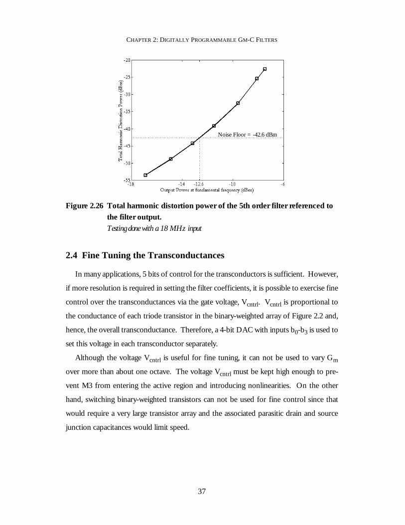
CHAPTER 2: DIGITALLY PROGRAMMABLE GM-C FILTERS
37
2.4 Fine Tuning the Transconductances
In many applications, 5 bits of control for the transconductors is sufficient. However,
if more resolution is required in setting the filter coefficients, it is possible to exercise fine
control over the transconductances via the gate voltage, Vcntrl. Vcntrl is proportional to
the conductance of each triode transistor in the binary-weighted array of Figure 2.2 and,
hence, the overall transconductance. Therefore, a 4-bit DAC with inputs b0-b3 is used to
set this voltage in each transconductor separately.
Although the voltage Vcntrl is useful for fine tuning, it can not be used to vary Gm
over more than about one octave. The voltage Vcntrl must be kept high enough to pre-
vent M3 from entering the active region and introducing nonlinearities. On the other
hand, switching binary-weighted transistors can not be used for fine control since that
would require a very large transistor array and the associated parasitic drain and source
junction capacitances would limit speed.
Figure 2.26 Total harmonic distortion power of the 5th order filter referenced to the filter output.Testing done with a 18 MHz input
Noise Floor = -42.6 dBm

CHAPTER 2: DIGITALLY PROGRAMMABLE GM-C FILTERS
38
2.4.1 4-Bit Vcntrl DAC
A 4-bit DAC is used to generate Vcntrl as shown in Fig. 2.27. Transistor Mt is oper-
ated in triode and is a scaled version of triode transistor M3 in Fig. 2.1C. Opamps O1
and O2 maintain a constant drain-source voltage ∆V ≈ 100 mV across Mt. Meanwhile a
dc current, Ia, and the 4-bit DAC output current, IDAC, are summed and forced through
Mt. As a result, triode transistor Mt has a drain-source conductance of,
(2.7)
A more detailed schematic is shown in Figure 2.28. The test voltage ∆V is the prod-
uct of a reference current Iref and a resistor R1. (On this chip, R1 is a triode transistor
with the gate voltage set externally for tuning.) The DAC is an R-2R ladder with unit cur-
rent sources, Ib. As the DAC input bits b0-b3 are swept over the range 0000 to 1111,
IDAC varies over the range 0 to 1.875⋅Ib. When IDAC = 0, resulting in
the minimum possible value of Vcntrl. Since the transconductor linearity is worst for
small values of Vcntrl, the current Ia must be chosen large enough to provide acceptable
linearity performance.
The opamps used are simple low-speed 2-stage p-channel input opamps with a nomi-
nal current consumption of 300 µA. Opamp O2 has a source-follower output stage
which consumes an additional 250 µA.
Figure 2.27 Using a four-bit DAC to program the gate control voltage, Vcntrl.
Gds,tIDAC Ia+
∆V---------------------- µnCox W L⁄( )tVgs, t= =
Gds t, Ia ∆V⁄=
Vsrcref
Vsrcref + ∆V-
b0 - b3
IDAC
O2
O1 Mt
Ia
IDAC + Ia Vin+
M1
M4
M3
Vin-
M2
M5
Iout+ Iout
-
I1 I1
Vcntrl
Transconductor
∆V
+
-

CHAPTER 2: DIGITALLY PROGRAMMABLE GM-C FILTERS
39
Opamp O1 keeps the source of Mt at Vsrcref. If the source voltage of M3 is also Vsr-
cref, then its drain-source conductance will be a scaled duplicate of Gds,t. If, on the other
hand, the dc voltage at the source of M3 differs from Vsrcref, there will be an offset
between Gds,t and Gds,3. Vsrcref is produced by a bias circuit which is a scaled copy of a
transconductor half-circuit (Figure 2.29). The bias circuit uses the common mode refer-
ence voltage, Vcmref, to produce Vsrcref. Therefore, all common mode levels must be
accurately set to Vcmref. Any offset in the common mode feedback loop would affect the
value of Vgs,3 and, hence, the filter time constants.
Figure 2.28 Details of the 4-bit DAC.
Figure 2.29 A systematic offset error in the CMFB. effects the gate-source voltage of M3, ,
which changes the degeneration conductance, and, hence, the cell’s transconductance.
Vsrcref
∆V
+
-
b0IDAC
∆V
+
-
Iref
R1
R
R RR
2R 2R
Vcntrl
O2
O1
b1 b2 b3
Mt
Ib0 Ib1 Ib2 Ib3 Ia
IDAC + Ia
b0 - b3
IDAC
Vcmref + Vcmerror
M3
I1
Vcmref
I1
Vcntrl
Vsrcref
Vsrcref + Vcmerror
Vcmerror Vgs,3 Vcntrl Vsrcref Vcmerror+–=Gds,3

CHAPTER 2: DIGITALLY PROGRAMMABLE GM-C FILTERS
40
2.4.2 HysteresisWhenever separate mechanisms are used for coarse discrete control and fine tuning of
the same adaptive parameter, it is desirable to introduce hysteresis at transitions of the
coarse control word in order to ensure that such transitions occur infrequently in steady
state [14]. In this design, b3 - b0 are used for fine tuning via Vcntrl while g2 - g-2 provide
coarse discrete control via the binary weighted transistor array. Hysteresis is introduced
by insuring that the fine tuning range is always greater than one LSB of the coarse con-
trol.
Unfortunately, hysteresis also creates some redundancy over the tuning range. When
there is too much hysteresis, fine control is lost. Therefore, Ib was made a function of
the coarse control signals g2 - g0 as shown in Fig. 2.30.
Figure 2.30 Implementation of DAC current sources in terms of unit current sources.Each unit current source Iu is a 0.3/1.6 µm NMOS device.
12×Iu 2×Iu
g1 & g2
Iu
g2
Iu
Ib
g0 & g1 & g2
∆V
+
-
IDAC
Iref
R1
R
R RR
2R 2R
Vcntrl
O2
O1 Mt
Ia = 30Iu
g2 - g0
g2g1g0 Ib
1xx Iu
01x 2Iu
001 4Iu
000 16Iu
Transistor W/L (µm) M
Mt .3/.51 46
Component Value
Iref 1350 µA
Iu 3.2 µA
R 7 kΩ
Vsrcref

CHAPTER 2: DIGITALLY PROGRAMMABLE GM-C FILTERS
41
2.4.3 ResultsThe fine control DAC was tested in two ways:
• by probing the dc voltage Vcntrl directly (Fig. 2.31).
• by measuring the low-frequency gain of the first order filter test structure (Fig. 2.32).
Figure 2.31 Probed DAC output voltage vs. 4-bit input word for different coarse control words.
Figure 2.32 Normalized gain of the 1st order test structure vs. 4-bit input word for different coarse control words.
g2g1g0 = 000
001
01x
g2g1g0 = 000
001
01x
1xx

CHAPTER 2: DIGITALLY PROGRAMMABLE GM-C FILTERS
42
Both tests indicated a strong discontinuity in the D/A characteristic when the MSB is
activated. Another significant discontinuity appears whenever the 2nd MSB is toggled.
In order for the D/A characteristic of the DAC in Fig. 2.28 to be linear, all of the cur-
rent sources must have the same output current: I0 = I1 = I2 = I3. However, this was
not the case because the NMOS transistors in current sources I0 - I3 were not operating
in the active mode. Therefore, the current sources had a low output impedance and volt-
age drops along the R-2R ladder caused the currents to vary: Ib0 < Ib1 < Ib2 < Ib3.
Three possible solutions to this problem are:
1. Use PMOS current sources instead of NMOS current sources. The PMOS transistors
would remain active ensuring high output impedances for all of the current sources.
This would require a significant redesign of the entire DAC.
2. Increase the potential at Vsrcref. This would also require the common mode reference
potential, Vcmref, to be increased everywhere in the chip to avoid the offset problem
described in Fig. 2.29.
3. Decrease the value of all resistors in the R-2R ladder. This would decrease the IR
drops in the resistor ladder, thereby putting all internal nodes at roughly the same
potential and mitigating the effect of the current sources’ finite output impedance.
Solutions #2 and #3 were verified using simulations in Fig. 2.33. The problem was not
noticed during design of the DAC because the value of Vsrcref was decreased after the
DAC design was complete.
Figure 2.33 Simulation results of the DAC subcircuit.(A) design as in prototype (B) with Vsrcref increased by 350 mV (C) with R decreased from 7 kΩ to 0.5 kΩ.

CHAPTER 2: DIGITALLY PROGRAMMABLE GM-C FILTERS
43
2.5 Power Consumption
Programmability is generally accompanied by increased power consumption since
some overdesign is necessary to insure proper operation over a wide range of conditions.
This design was no exception. The total power consumption for the entire prototype IC
was simulated at 60 deg. C to be 93.1 mA from a 2.5 V supply or 233 mW. A current
consumption of 100 mA for the entire prototype IC was measured in the lab, providing
reasonable agreement with the simulations. Much of the current was consumed by test
structures and output buffers (Fig. 2.34). The current consumed by the 5th order filter
alone, including ten fine control DACs, bias circuitry, etc., is 52.3 mA or 130 mW. How-
ever, some obvious avenues for improvement exist.
The fine control DACs could be eliminated. This would provide a power savings of
17.1 mA resulting in a 5th order filter consuming 35.2 mA or 88 mW with 5-bit program-
mable coefficients, still sufficient programmability for most applications. This requires
no redesign other than connecting the control voltage nodes, Vcntrl, to a fixed potential.
In fact, for most of the testing, only 5 bits of programmability were used and the DAC
input was held constant at b3b2b1b0 = 0000. Other improvements in power consump-
tion would require more significant redesign. The biggest improvement would be
obtained by replacing the miller integrators with simple capacitor integrators, which
Figure 2.34 Current consumption of the prototype IC by functional block.These results were simulated at 60 deg. C. A current consumption of 100 mA was measured in the lab.
Test structures,Buffers, etc.,
41.0 mA
DACs, 17.1 mA
CMFBs, 3.9 mA
Transconductors,7.6 mA
Filter Core,52.1 mA
Miller Integrators,21.2 mA
Biasing, 2.4 mA
Entire Prototype IC = 93.1 mA

CHAPTER 2: DIGITALLY PROGRAMMABLE GM-C FILTERS
44
might also simplify the CMFB loop and enable higher speed operation. In this case, the
power savings would be approximately an additional 20 mA or 50 mW.
2.6 Conclusions
Techniques for implementing a 5th order digitally programmable filter in a 0.25 µm
CMOS process were described for analog adaptive filtering applications. The measured
results from a prototype implementation of the filter are summarized in Table 2.1.
An orthonormal structure was chosen to provide a high degree of programmability
while maintaining good dynamic range scaling. The mechanism provided for coarse dig-
ital gain control suffers from a finite transconductance even when the control word is all
zeros. However, this can be overcome by turning off the output current mirror. The
fine tuning mechanism described in Section 2.4 could be useful when accurate gain con-
trol is required, but its repeated use caused a dramatic increase in circuit size, complexity,
and power consumption.
Traditional transconductor and miller integrator circuits were redesigned with only
NMOS devices in the signal path to take advantage of their superior speed. A major lim-
itation of transconductor circuits which rely on differential pairs that are source-degener-
ated by a triode MOS device is that their transconductance and linearity depend upon the
input common mode level. Therefore, strongly inverted triode devices should be used to
reduce this dependence, or the MOS devices should be replaced by passive resistors.
Also, although feedback can reduce nonlinearity in a CMOS transconductor by maintain-
ing a constant current through the input differential pair, the feedback can also cause the
input devices to go into triode for large input swings. Whether the net effect of the feed-
back is to improve or worsen linearity will depend upon the particular application and
process technology used.
Although the use of miller integrators offers the potential for better linearity, at low
supply voltages it is difficult to get better than 40-50 dB of linearity anyway. Further-
more, the use of a Miller stage can limit speed compared with a passive capacitor integra-
tor. Generally, in mixed-signal systems, low-speed high-accuracy filtering can be easily

CHAPTER 2: DIGITALLY PROGRAMMABLE GM-C FILTERS
45
performed digitally and the extra analog complexity and current consumption which
Miller integrators imply are undesirable.
Although many useful circuit techniques have been demonstrated, such as the all-
NMOS transconductor and Miller integrator and the use of multiple transconductance
control mechanisms with hysteresis, the poor linearity measurements limited the design’s
Entire Prototype Gm-C Filter IC
Technology 0.25 µm CMOS
Supply Voltage 2.5 V
Integrated Area 2.5 mm × 1.7 mm= 4.25 mm2
Power233 mW (Simulated)250 mW (Measured)
First Order Filter Test Structure
Integrated Area 0.25 mm × 0.38 mm= 0.094 mm2
Power 29.7 mWa
THD with 200 mVpp input, 120 mVpp output tone at 8 MHz -41 dB
5th Order Lowpass Orthonormal Ladder Filter
Integrated Area 1.25 mm × 0.38 mm= 0.469 mm2
Power with 9-Bit Programmable Coefficients 130 mW (Simulated)a
Power with 5-Bit Programmable Coefficients 87.5 mW (Simulated)a
Input-referred Noise Power over 250 MHz BW 1.656 mVrms
Input-referred Noise Spectral Density in the passband 120
THD with 125 mVpp input, 170 mVpp output tone at -27.7 dBb
SFDR with input tone at 30 dBc
Table 2.1 Summary of prototype filter IC measurements.a. Includes shared bias circuitry.b. Corresponds to measurement made in Fig. 2.21. Measurements for different trans-
fer functions varied between -20 dB to -30 dB.c. Corresponds to input amplitude of 105 mVpp and output amplitude of 145 mVpp.
nV Hz( )⁄
f3 dB 2⁄
f3 dB 2⁄

CHAPTER 2: DIGITALLY PROGRAMMABLE GM-C FILTERS
46
relevance to real applications. It was useful primarily as a test vehicle for exploring digital
adaptation algorithms for analog filters. For comparison, the design of a 4th order digi-
tally programmable Gm-C filter in a similar process technology (0.25 µm CMOS) was
described in [15]. Four bits of programmability were provided for each transconductor
by switching binary-scaled differential pair transconductors on and off. Passive capaci-
tors were used as integrators. This approach provided a much simpler and higher speed
design, although the circuit used a higher supply voltage (3.3 V) and was limited to but-
terworth lowpass transfer functions. In [16], an 8th order lowpass Gm-C filter was
described in 0.25 µm CMOS with a 2.5 V supply. The transconductors were weakly
degenerated differential pairs. Digital programmability was provided using a combina-
tion of tail current DACs, binary-ratioed degeneration resistors, and binary-scaled paral-
lel-connected transconductors. In both [15] and [16], no Miller integrators were used yet
the linearity was far superior to that reported here (40 - 50 dB THD). However, the fil-
ters were restricted to fixed lowpass transfer functions with programmable cutoff fre-
quencies and (in [16]) programmable high-frequency boost. An analog filter with all
poles and zeros digitally programmable has only been reported at much lower speeds (up
to 8 MHz) in a BiCMOS process [8].
2.7 Appendix - Derivation of Eqn. (2.1)
The low frequency small signal equivalent half-circuit of the transconductor in Fig.
2.1C is shown in Fig. 2.35. The PMOS current sources were cascoded so their output
impedance is far greater than all others in the circuit. Therefore, infinite output imped-
ance is assumed to simplify the small signal analysis.
A node equation at gives,
(2.8)
(2.9)
A node equation at gives,
vs1
gm4vd1 gds4 2gds3 gs1+ +( )vs1+ 0=
vs1⇒gm4
gds4 2gds3 gs1+ +-------------------------------------------vd1–=
vd1

CHAPTER 2: DIGITALLY PROGRAMMABLE GM-C FILTERS
47
(2.10)
Substituting Eqn. (2.9) into Eqn. (2.10) gives,
(2.11)
Making the following approximation,
(2.12)
one can now write, from Eqn. (2.11),
(2.13)
Assuming the subsequent stage has a relatively low input resistance (i.e. )
the output current is simply given by,
(2.14)
This is the result presented in Eqn. (2.1).
Figure 2.35 Small-signal equivalent half-circuit of the transconductor.
Rout of I1 = ∞
0
vd1Vin
gds1gm1(vin - vs1)
vs1
gs1vs1
gds4gm4vd12gds3gds6 gm6vd1
Iout
0Rin
gm1 Vin vs1–( ) gds1 vd1 vs1–( ) gs1vs1–+ 0=
gm1Vingm1 gds1 gs1+ +( )gm4
gds4 2gds3 gs1+ +-----------------------------------------------------vd1 gds1vd1+ + 0=
gm1 gds1 gs1+ +( )gm4
gds4 2gds3 gs1+ +-----------------------------------------------------
gm1gm4
gds4 2gds3 gs1+ +------------------------------------------- gds1»≅
gm1Vingm1gm4
gds4 2gds3 gs1+ +-------------------------------------------vd1+ 0≅
gm4vd1⇒ gds4 2gds3 gs1+ +( )Vin–=
Rin 1 gds6⁄«
Iout gm6vd1–=
gm6
gm4-------- gds4 2gds3 gs1+ +( )Vin=
M 2gds3 gds4 gs1+ +( )Vin=

CHAPTER 2: DIGITALLY PROGRAMMABLE GM-C FILTERS
48
2.8 Appendix - Digital Circuitry
Simple digital circuitry was included on the prototype to program the filter coeffi-
cients. The circuitry includes a register file for storing the following data:
• 11 bits (b3-b0, g2-g-2, and d1-d0) for each of the 5 filter feedback parameters: 55 bits
total
• 12 bits (b3-b0, g2-g-2, d1-d0, plus one sign bit) for each of the 5 filter feed-in parame-
ters: 60 bits total
• 2 bits (c1-c0) for tuning the integrating capacitors
The result is a total of 117 bits. The register file was organized as 16 words x 12 bits
per word, so each write operation requires 4 address bits plus 12 data bits. Because a 24-
pin package was used, only 6 pins were allocated to the digital circuitry, two of which
were used for digital power supplies. The remaining 4 signals provide a serial interface
through which an address and 12 bits of data can be written. No facility for reading from
the register file (other than probe pads) was provided.
The 4 serial interface signals are:
• Clock - (rising edge triggered) a clock is required to serially shift data into the chip
• Reset - (active low) this signal clears the contents of all flip-flops in the register file
• Start - (active high) a write operation is initiated by activating the Start signal for one
clock cycle
• Data - provides the address and data to be written into the register file
After a write operation is initiated by the “Start” signal, the next bit clocked into the
“Data” pin must be a 1. The proceeding 4 bits are used as the address in the register file
(a3 - a0) and the remaining 12 bits are the data (r11 - r0). A sample timing diagram is pro-
vided in Fig. 2.36. Table 2.2 is an address map for the register file.
The serial interface was implemented using standard cells which were manually placed
and routed. Since the interface was not speed-critical, no effort was made to optimize
the netlist or layout. A schematic of the digital circuitry is provided in Fig. 2.37.

CHAPTER 2: DIGITALLY PROGRAMMABLE GM-C FILTERS
49
2.9 References
[1] D. A. Johns, W. M. Snelgrove, and A. S. Sedra, "Continuous-Time LMS Adaptive Recursive Filters," IEEE Trans. Circuits Syst., Vol. 38, No. 7, pp. 769-777, July 1991.
Figure 2.36 Sample timing diagram for serial digital interface.
Binary Address(es) Register Contents (r11 - r0)
0000 - 0100 Filter feed-in coefficients.
r0: sign bit
r2 - r1: d1-d0 - output current mirror con-
trol
r7 - r3: g2-g-2 - transistor array control bits
r11 - r8: b3-b0 - fine control DAC
0101 - 0111 Not used
1000 - 1100 Filter feedback coefficients.
r0: Not used
r2 - r1: d1-d0 - output current mirror con-
trol
r7 - r3: g2-g-2 - transistor array control bits
r11 - r8: b3-b0 - fine control DAC
1101 - 1110 Not used
1111 Capacitance tuning:
r1 - r0: c1-c0
r11 - r2: Not used
Table 2.2 Digital register file address map.
Start
Clock
Data a0 a3 r0 r11
1st bit after Start is always “high”
r1a1 a2 ...

CHAPTER 2: DIGITALLY PROGRAMMABLE GM-C FILTERS
50
[2] A. Shoval, D. A. Johns, and W. M. Snelgrove, "Comparison of DC Offset Effects in Four LMS Adaptive Algorithms," IEEE Trans. Circuits Syst. II, Vol. 43, No. 3, pp. 176-185, March 1995.
[3] T. Kwan and K. Martin, "An Adaptive Analog Continuous-Time CMOS Biquadratic Filter," IEEE Journal of Solid-State Circuits, Vol. 26, No. 6, pp. 859-867, June 1991.
[4] J. E. C. Brown, P. J. Hurst, B. C. Rothenberg, and S. H. Lewis, "A CMOS Adaptive Continuous-Time Forward Equalizer, LPF, and RAM-DFE for Magnetic Recording," IEEE Journal of Solid-State Circuits, Vol. 34, No. 2, pp. 162-169, Feb. 1999.
[5] P. K. D. Pai, A. D. Brewster, and A. Abidi, “Analog Front-End Architectures for High-Speed PRML Magnetic Read Channels”, IEEE Trans. Magnetics, pp. 1103-1108, March 1995.
[6] F. Pecourt, J. Hauptmann, and A. Tenen, “An Integrated Adaptive Analog Balancing Hybrid for Use in (A)DSL Modems,” Int. Solid-State Circuits Conf., pp. 252-253, San Francisco, February 1999.
[7] M. G. Larimore, J. R. Treichler, and C. R. Johnson, “SHARF: An Algorithm for Adapting IIR Digital Filters,” IEEE Trans. Acoust. Speech Signal Process., vol. ASSP-28, p. 428-440, Aug. 1980.
[8] A. Hematy and G. W. Roberts, “A fully-programmable analog log-domain filter circuit”, IEEE Int. Symp. Circuits and Syst., vol. 1, p. 309-312, June 1998.
Figure 2.37 Schematic diagram for a 4-pin digital serial interface.
D Q
Clock
Data
Addressable 16x12 Array of Transparent Latches
Addr Data LatchClear
Clr
D Q
Clr
D Q
Clr
D Q
Clr
D Q
Clr
D Q
Clr
Start
Reset
4 12
DFF1 DFF2 DFF3 DFF16 DFF17 DFF18

CHAPTER 2: DIGITALLY PROGRAMMABLE GM-C FILTERS
51
[9] S. Pavan and Y. Tsividis, “Time-Scaled Electrical Networks — Properties and Applications in the Design of Programmable Analog Filters,” IEEE Trans. Circuits Syst. II, vol. 47, pp. 161-165, Feb. 2000.
[10] D. A. Johns, W. M. Snelgrove and A. S. Sedra, "Orthonormal Ladder Filters," IEEE Trans. Circuits Syst., Vol. 36, No. 3, pp. 337-343, March 1989.
[11] D. R. Welland, et. al. “A Digital Read/Write Channel with EEPR4 Detection,” IEEE Int. Solid-State Circuits Conf., pp. 276-277, San Francisco, February 1994.
[12] J. Cheng and D. A. Johns, “A 100 MHz Partial Analog Adaptive Equalizer for use in Wired Data Transmission,” European Solid State Circuits Conference, Sept. 1999.
[13] M. Padmanabhan and K. Martin, “A CMOS Analog Multi-Sinusoidal Phase Locked-Loop,” IEEE Journal of Solid-State Circuits, Vol. 29, No. 9, pp. 1046-1057, September 1994.
[14] K. Kamra, Cable equalization using adaptive analog filters, M. A. Sc. Thesis, University of Toronto, 1996.
[15] S. Pavan, Y. Tsividis, and K. Nagaraj, “Widely Programmable High-Frequency Continuous-Time Filters in Digital CMOS Technology,” IEEE Journal of Solid-State Circuits, Vol. 35, No. 4, pp. 503-511, April 2000.
[16] G. Bollati, S. Marchese, M. Demicheli, and R. Castello, “An Eigth-Order CMOS Low-Pass Filter with 30-120 MHz Tuning Range and Programmable Boost,” IEEE Journal of Solid-State Circuits, Vol. 36, No. 7, pp. 1056-1066, July 2001.

52
Chapter 3
The Dithered Linear Search Algorithm
3.1 Introduction
At low speeds, adaptive filtering is easily and efficiently performed using digital cir-
cuits. Analog filters are preferable at high speeds when low power consumption, small
integrated area, and moderate linearity are required. The LMS algorithm is currently the
most popular technique for digital filter adaptation. Unfortunately, implementation of
the LMS algorithm in analog adaptive filters is challenging. Dc offsets on the analog sig-
nals can prevent accurate convergence of the LMS algorithm [1], [2]. Also, significant
additional analog hardware may be required to obtain the gradient signals required by the
LMS algorithm [3].
As a result, numerous heuristic algorithms have been developed for specific applica-
tions based upon adjusting analog filter parameters to satisfy some desirable and easily
observed condition [4], [5], [6]. Although relatively simple, both conceptually and in
terms of their hardware implementation, these approaches are tailored to specific appli-
cations and filter structures. Therefore, they are not easily generalized to new applica-
tions, particularly those requiring high order filters with several adapted parameters.
In this chapter, a technique for analog filter adaptation is discussed which is general,
has a straightforward hardware implementation, and is robust with respect to dc offsets.
The dithered linear search (DLS) technique does not require access to the filter’s internal

CHAPTER 3: THE DITHERED LINEAR SEARCH ALGORITHM
53
states and little additional analog hardware is required. All filter parameters may be
adapted simultaneously and independently of one another.
In Section 3.2 of this chapter, a theoretical framework for the problem of filter adap-
tation is established and two gradient descent adaptation algorithms are presented. In
Section 3.3, the DLS algorithm is introduced. Theoretical results for the misadjustment
and convergence rates are derived in Section 3.4. Behavioral simulation results are then
presented in Section 3.5 for both a tapped delay line and a continuous time filter. Differ-
ent possible dither signals are considered in Section 3.6, and dc offset effects are dis-
cussed in Section 3.7. In Section 3.8, subsampling of the output error signal is discussed,
and in Section 3.9 the effect of quantization of the filter parameters is analyzed. Finally,
in Section 3.10, experimental results of the algorithm applied to a continuous time inte-
grated analog filter are presented.
3.2 Background
Using the general framework for filter adaptation established in Section 1.3.1, recall
that gradient descent optimizers proceed by updating the filter’s parameters iteratively in
a direction opposite the gradient . The iterative update rule is repeated here,
(3.1)
where µ is a parameter controlling the rate of adaptation. The only problem is how to
obtain the gradient , or for short. Generally the exact value of can
not be determined, so an unbiased estimate of the gradient is used instead,
(3.2)
This estimate is substituted into Eqn. (3.1) resulting in,
(3.3)
Different approaches to obtaining the gradient estimates define different gradient
descent algorithms. The remainder of this section will describe how gradient estimates
are obtained for the LMS and differential steepest descent (DSD) algorithms.
ε p k( )( )p k( )∇
p k 1+( ) p k( ) µ ε p k( )( )p k( )∇⋅–=
ε p k( )( )p k( )∇ εp∇ εp∇
εp∇ ε∂p1∂
--------ˆ ε∂
p2∂--------
ˆ… ε∂
pN∂---------
ˆ T
=
p k 1+( ) p k( ) µ εp∇⋅–=
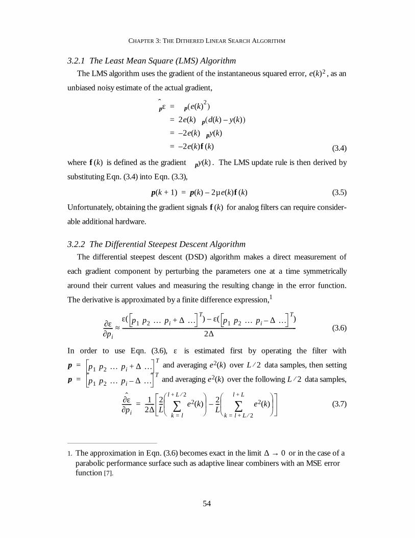
CHAPTER 3: THE DITHERED LINEAR SEARCH ALGORITHM
54
3.2.1 The Least Mean Square (LMS) AlgorithmThe LMS algorithm uses the gradient of the instantaneous squared error, , as an
unbiased noisy estimate of the actual gradient,
(3.4)
where is defined as the gradient . The LMS update rule is then derived by
substituting Eqn. (3.4) into Eqn. (3.3),
(3.5)
Unfortunately, obtaining the gradient signals for analog filters can require consider-
able additional hardware.
3.2.2 The Differential Steepest Descent AlgorithmThe differential steepest descent (DSD) algorithm makes a direct measurement of
each gradient component by perturbing the parameters one at a time symmetrically
around their current values and measuring the resulting change in the error function.
The derivative is approximated by a finite difference expression,1
(3.6)
In order to use Eqn. (3.6), is estimated first by operating the filter with
and averaging over data samples, then setting
and averaging over the following data samples,
(3.7)
1. The approximation in Eqn. (3.6) becomes exact in the limit or in the case of a parabolic performance surface such as adaptive linear combiners with an MSE error function [7].
e k( )2
εp∇ e k( )2( )p∇=
2e k( ) d k( ) y k( )–( )p∇=
2– e k( ) y k( )p∇=
2e k( )φ k( )–=
φ k( ) y k( )p∇
p k 1+( ) p k( ) 2µe k( )φ k( )–=
φ k( )
∆ 0→
ε∂pi∂
-------ε p1 p2 … pi ∆+ …
T( ) ε p1 p2 … pi ∆– …T( )–
2∆--------------------------------------------------------------------------------------------------------------------------------≈
ε
p p1 p2 … pi ∆+ …T
= e2 k( ) L 2⁄
p p1 p2 … pi ∆– …T
= e2 k( ) L 2⁄
ε∂pi∂
-------ˆ 1
2∆------- 2
L--- e2 k( )
k l=
l L 2⁄+
∑ 2
L--- e2 k( )
k l L 2⁄+=
l L+
∑
–=

CHAPTER 3: THE DITHERED LINEAR SEARCH ALGORITHM
55
An advantage of the DSD algorithm over LMS adaptation is that it does not require
access to the filter’s internal states. It is simple and intuitive. However, its hardware
implementation is somewhat complicated by the fact that the gradient components must
be estimated one at a time. During their discussion of the DSD algorithm, the authors of
[8] point out that, “All weights can be simultaneously dithered at individual frequencies
and the gradient components obtained by cross correlation.” That idea is the basis of the
“dithered linear search” algorithm described below.
3.3 The Dithered Linear Search
The dithered linear search (DLS) algorithm1 is also a gradient descent optimizer. The
term “dither” refers to a signal with small amplitude and zero mean that is intentionally
injected into a system,
(3.8)
(3.9)
In Eqn. (3.8), is the algorithm’s current estimate of an optimal parameter value
whereas is the parameter value actually applied to the filter including the dither .
Each gradient component is then inferred by correlating changes in the corresponding
dither signal to changes in ,
(3.10)
In Eqn. (3.10), the gradient estimate is given by . The product
correlates changes in the output error with the parameter dither to give
the sign of the gradient. The product is divided by σ2 (the variance of ) to normal-
ize the gradient estimate with respect to the dither signal’s magnitude. Again, instanta-
neous estimates can be substituted for in which case Eqn. (3.10) becomes,
1. The name “dithered linear search” was chosen in reference to the other linear search adaptation algorithms (i.e. sequential linear search, random linear search) to which the DLS bears a strong resemblance.
pi' k( ) pi k( ) δi k( )+=
E δi k( )[ ] 0=
pi
pi' δi
ε p' k( )( )
pi k 1+( ) pi k( ) µ
σ2------ δi k( ) ε p' k( )( )⋅ ⋅–=
δi k( ) ε p' k( )( )⋅ σ2⁄
δi k( ) ε p' k( )( )⋅
δi k( )
ε p' k( )( )

CHAPTER 3: THE DITHERED LINEAR SEARCH ALGORITHM
56
(3.11)
The gradient estimate is given by,
(3.12)
Multiple filter parameters can be adapted simultaneously by applying independent (i.e.
uncorrelated) dither signals to all of the parameters.
(3.13)
(3.14)
The adaptation of any one parameter, , will not be affected by the dither on the others
since, over time, only those changes in ε which are correlated with will influence the
parameter .
The DLS algorithm has a straightforward hardware implementation. A block diagram
is shown in Fig. 3.1 for one parameter. The filter input , output , reference signal ,
and error signal all have their usual characteristics, as described in Section 1.3.1. The
algorithm is easily scaled to adapt more parameters using more copies of the same hard-
ware. If the dither signals are binary, the hardware is even simpler. The correlator
becomes trivial and the dither signal can be directly connected to the LSB of the parame-
ter control word. Uncorrelated binary dither signals are also easy to generate. Several
different possibilities are discussed in Section 3.6.
3.3.1 The Block DLS AlgorithmRather than continuously updating the parameters via Eqn. (3.11), one may keep them
fixed (except for dither) for a block of L consecutive data samples. During this period,
derivative estimates are constructed by cross-correlating the dither and squared error sig-
nals,
pi k 1+( ) pi k( ) µ
σ2------ δi k( ) e2 k( )⋅ ⋅–=
ε∂pi∂
-------ˆ 1
σ2------ δi k( ) e2 k( )⋅ ⋅=
p' k( ) p k( )δ1 k( )
⋅δN k( )
+ p k( ) δ k( )+= =
E δi k( )δj k( )[ ] 0, i j≠=
pi
δi
pi
u y d
e

CHAPTER 3: THE DITHERED LINEAR SEARCH ALGORITHM
57
(3.15)
After every L samples, the gradient estimates are used to update the parameters via Eqn.
(3.3). The standard DLS algorithm corresponds to the limiting case of the block DLS
algorithm where . Although the complexity and theoretical performance of the
block DLS algorithm is the same as the DLS algorithm, the block adaptation can offer
better stability and performance in practice, as we shall see in Section 3.6.
3.4 Theoretical Analysis
3.4.1 PreliminariesIn order to simplify the theoretical analysis of the DLS algorithm and to cast it in a
form similar to that used in [8], only adaptive linear combiners are considered. This is
common practice in the analysis of adaptive algorithms and the results are also applicable
whenever the performance surface is approximately quadratic near its minimum. Also,
only binary dither signals are analyzed in detail.
As with all gradient descent optimizers, a necessary condition for stability of the DLS
algorithm is,
(3.16)
Figure 3.1 Block diagram of the dithered linear search algorithm.No knowledge of the filter’s internal states is required.
DitherSource
−µ/σ2
AdaptiveFilter
d
(·)2eyu
δ
pp’ e2⌠⌡
ε∂pi∂
-------ˆ 1
L---
δi k( ) e2 k( )⋅
σ2---------------------------
k l=
l L+
∑=
L 1=
0 µ 1 λmax⁄< <

CHAPTER 3: THE DITHERED LINEAR SEARCH ALGORITHM
58
where λmax is the largest eigenvalue of the state correlation matrix, , defined below in
terms of the filter’s state variables ,
(3.17)
The MSE performance surface of an adaptive linear combiner can be shown to be
quadratic,
(3.18)
where . A co-ordinate transformation can be used to separate the indepen-
dent modes of the adaptive process, . A gradient descent algorithm causes
the th component of to converge towards its optimal value exponentially with a time
constant of,
(3.19)
The MSE will decay with a th mode time constant of,
(3.20)
Eqn. (3.20) is written in terms of iterations of the DLS algorithm. For the block DLS
algorithm, each iteration corresponds to data samples. Therefore, in terms of data
samples the th mode time constant is,
(3.21)
3.4.2 ConvergenceIn order to ensure that the DLS algorithms converge, it is desirable to show that the
gradient estimates in Eqn. (3.12) and Eqn. (3.15) provide unbiased estimates of the true
gradient.
R
xi
R E
x1x1 x1x2 … x1xN
x2x1 x2x2 … x2xN
⋅ ⋅ ⋅… xNxN
r11 r12 … r1N
r21 r22 … r2N
⋅ ⋅ ⋅… rNN
= =
ε εmin pT p∗T–( )R p p∗–( )+=
εmin vTRv+=
v p p*–=
w Q 1– v=
k w
τk1
2µλk------------=
k
τkMSE
14µλk------------=
L
k
TkMSELτkMSE
L4µλk------------= =

CHAPTER 3: THE DITHERED LINEAR SEARCH ALGORITHM
59
(3.22)
(3.23)
A proof of Eqn. (3.23) for the DLS with binary dither follows.
For a binary dither signal,
(3.24)
Hence,
(3.25)
Taking the expectation of both sides of Eqn. (3.12),
(3.26)
Also, a dither signal has zero mean.
(3.27)
(3.28)
Combining Eqn. (3.28) with Eqn. (3.26) yields,
(3.29)
It can be shown (see Appendix) that the MSE estimates have the following bias,
(3.30)
Substituting Eqn. (3.30) into Eqn. (3.29) gives,
E ∇pεˆ[ ] ∇pε, or equivalently=
E ε∂pi∂
-------ˆ ε∂
pi∂-------= , for all i
δi k( ) ∆±=
σ2 E δi2 k( )[ ]≡ ∆2=
E ε∂pi∂
-------ˆ
E 1
σ2------ δi k( ) e2 k( )⋅ ⋅=
1∆2------ E δi k( ) e2 k( )⋅[ ]⋅=
E δi k( )[ ] 0=
δi k( ) +∆, one-half of the time=
δi k( ) ∆– , one-half of the time=
⇒
E ε∂pi∂
-------ˆ 1
∆2------ 1
2--- E δi k( ) e2 k( )⋅[ ] δi +∆=⋅
12--- E δi k( ) e2 k( )⋅[ ] δi ∆–=⋅
+ =
1∆2------ ∆
2---E e2 k( )[ ]
δi +∆= ∆–
2------E e2 k( )[ ]
δi ∆–= +
=
12∆------- E e2 k( )[ ]
δi +∆=E e2 k( )[ ]
δi ∆–=–( )=
E e2 k( )[ ]δi ∆±=
ε p1 p2 … pi ∆± …T( ) ∆+
2tr R( ) rii–( )=

CHAPTER 3: THE DITHERED LINEAR SEARCH ALGORITHM
60
(3.31)
In order to complete the proof of Eqn. (3.23), it is required that,
(3.32)
Eqn. (3.32) is true by definition of the gradient in the limit . Eqn. (3.32) is also
true for any value of when the error function is a quadratic function of , as is the
case here since an adaptive linear combiner is assumed. Therefore, the DLS algorithm
provides unbiased gradient estimates.
The proof for the block DLS algorithm is similar. If one assumes that
for L/2 samples and for L/2 samples within each block, then take the
expectation of Eqn. (3.15),
(3.33)
E ε∂pi∂
-------ˆ 1
2∆------- ε
p1
p2
…pi+∆
…
∆2+ tr R( ) rii–( )
ε
p1
p2
…pi ∆–
…
∆2+ tr R( ) rii–( )
–=
ε p1 p2 … pi ∆+ …T
( ) ε p1 p2 … pi ∆– …T
( )–
2∆--------------------------------------------------------------------------------------------------------------------------------=
ε p1 p2 … pi ∆+ …T( ) ε p1 p2 … pi ∆– …
T( )–
2∆-------------------------------------------------------------------------------------------------------------------------------- ε∂
pi∂-------=
∆ 0→
∆ ε p
δi k( ) +∆=
δi k( ) ∆–=
E ε∂pi∂
-------ˆ
E 1L---
δi k( ) e2 k( )⋅
σ2---------------------------
k l=
l L+
∑=
1L∆2--------- E δi k( ) e2 k( )⋅
k l=δi +∆=
l L+
∑
δi k( ) e2 k( )⋅k l=
δi ∆–=
l L+
∑
+
=
1L∆2--------- +∆( ) L
2---⋅ E e2 k( )[ ]
δi +∆=∆–( ) L
2---⋅ E e2 k( )[ ]
δi ∆–=+
=
12∆------- E e2 k( )[ ]
δi +∆=E e2 k( )[ ]
δi ∆–=–( )=

CHAPTER 3: THE DITHERED LINEAR SEARCH ALGORITHM
61
This result is the same as Eqn. (3.29). From here, the proof is identical to the proof for
the standard DLS algorithm.
Eqn. (3.31) is a finite difference gradient estimate, just like the one used for the DSD
algorithm in Eqn. (3.6). The similarity is not surprising since the DSD algorithm can be
considered a special case of the DLS algorithm where the parameters are dithered one at
a time.
Since the gradient estimates are unbiased, as they are averaged over a longer time they
approach the true value of the gradient resulting in a perfect gradient descent optimizer.
This limit is approached by decreasing . So, the DLS is guaranteed stable as long as
is taken “small enough”. The bounds imposed by Eqn. (3.16) apply to any gradient
descent optimizer, so they are necessary but not sufficient conditions on to ensure that
the DLS algorithm converges to a minimum in . In general, the range of stable
values for will depend upon the filter structure, the type of dither signal, and the statis-
tics of the input data (which may not be precisely known a priori). Therefore, stability of
the adaptive process must be verified via simulation.
3.4.3 PerturbationEven when the DLS algorithm is in steady state and all parameters have converged to
their optimal values, the MSE will be somewhat greater than the minimum MSE because
the additive dither causes the filter to operate with sub-optimal parameter values. The
excess MSE caused by the dither in steady state is referred to as “perturbation”. Pertur-
bation is a phenomenon which occurs in the DLS and DSD algorithms, but not the LMS
algorithm where no dither is used. In this section, theoretical expressions for the pertur-
bation will be derived.
The mean squared error, including the effect of dither, is obtained by using in
place of in Eqn. (3.18),
(3.34)
After convergence, neglecting misadjustment or any other sources of error such as dc
offset effects, . Substituting this into Eqn. (3.34),
µ µ
µ
ε p t( )( )
µ
p' k( )
p k( )
ε εmin p' k( ) p∗–( )TR p' k( ) p∗–( )+=
p k( ) p∗=( ) p' k( ) p∗– δ k( )=( )⇒

CHAPTER 3: THE DITHERED LINEAR SEARCH ALGORITHM
62
(3.35)
Taking the expected value of both sides over time gives the steady-state MSE,
(3.36)
The second line of Eqn. (3.36) was obtained by cancelling all of the other terms in the
product due to the independence of the dither signals: ,
. For binary dither where ,
(3.37)
The perturbation, , is defined as the ratio of the excess MSE over the minimum MSE.
(3.38)
Using the fact that the trace of a matrix is equal to the sum of its eigenvalues, Eqn. (3.38)
can be rewritten in terms of the average eigenvalue of the state correlation matrix, .
(3.39)
Eqn. (3.39) indicates that the perturbation is larger using the DLS algorithm than
using the DSD algorithm by a factor of . As shown in Fig. 3.2, this is because all
parameters are dithered simultaneously in the DLS algorithm, instead of one at a time as
in the DSD algorithm.
3.4.4 Noise in the Gradient EstimatesAs with all gradient descent optimizers, the DLS algorithm relies upon noisy estimates
of the gradient to perform adaptation. The difference between the estimated gradient
and actual gradient is a vector random variable, .
(3.40)
The variance of measures the accuracy of the gradient estimates for different gradient
descent algorithms.
ε εmin δT k( )Rδ k( )+=
εSS εmin E δT k( )Rδ k( )[ ]+=
εmin riiE δi2 k( )[ ]
i∑+=
δT k( )Rδ k( ) E δi k( )δj k( )[ ] 0=
i j≠ δi ∆±=
εSS εmin ∆2 riii
∑+ εmin ∆2 tr R( )⋅+= =
P
PεSS εmin–
εmin----------------------- ∆2
εmin--------- tr R( )⋅= =
λavg
PN∆2λavg
εmin--------------------=
N N
n
εp∇ εp∇– n=
n

CHAPTER 3: THE DITHERED LINEAR SEARCH ALGORITHM
63
Since , it is known that and,
(3.41)
Using Eqn. (3.25),
(3.42)
Figure 3.2 Perturbation in a 2-dimensional parameter space using (A) the DSD algorithm (B) the DLS algorithm.The figure illustrates the points p’ where the filter is operated when the nominal parameter values are p = [p1 p2]. (A) Using the DSD, the filter operates one-quarter of the time at each of p’ = [p1+∆ p2], [p1−∆ p2], [p1 p2+∆], and [p1 p2−∆]. (B) The DLS operates one-quarter of the time at each of p’ = [p1+∆ p2+∆], [p1+∆ p2−∆], [p1−∆ p2+∆], and [p1−∆ p2−∆]. Note that the total perturbation is larger in (B) because both parameters are simultaneously dithered.
(A) (B)
p
∆
p∗
p
∆
p∗
p
∆
p∗
p
∆
p∗
p
∆
p∗
p
∆
p∗
p
∆
p∗
p
∆
p∗
p
∆
p∗
p
∆
p∗
p
∆
p∗
p
p∗
2∆
E εp∇[ ] εp∇= E n[ ] 0=
var n[ ] var εp∇ εp∇–[ ] var εp∇[ ] var ε∂p1∂
--------ˆ
… ε∂pN∂
---------ˆ T
= = =
var ε∂pi∂
-------ˆ
var 1
σ2------ δi e2⋅ ⋅=
1∆4------ var δi e2⋅[ ]⋅=
1∆4------ 1
2---var δi e2⋅[ ]
δi ∆–=
12---var δi e2⋅[ ]
δi ∆=+
=
1∆4------ 1
2---∆2var e2[ ]
δi ∆–=12---∆2var e2[ ]
δi ∆=+
=

CHAPTER 3: THE DITHERED LINEAR SEARCH ALGORITHM
64
As in [8], assume that is normally distributed with zero mean.1 Therefore,
(3.43)
In steady state with the filter parameters near their optimal values and assuming the per-
turbation is small,
(3.44)
Substituting Eqn. (3.44) into Eqn. (3.42),
(3.45)
For the block DLS, take the variance of both sides of Eqn. (3.15),
(3.46)
In Eqn. (3.46), each MSE estimate is made by averaging over data samples.
Again assuming that in steady state, , the variance of the estimates are reduced
by a factor of compared with the regular DLS algorithm.
(3.47)
Substituting Eqn. (3.47) into Eqn. (3.46) gives the variance of the block DLS gradient
estimates,
1. The assumption of zero mean can be guaranteed by using an adaptive dc tap weight. In [7] it was
shown that probability distributions for other than gaussian result in a smaller misadjustment.
e d y–( )=
e
var e2[ ] 2ε2=
var e2[ ]δi ∆–=
var e2[ ]δi ∆=
2εmin2≅ ≅
var ε∂pi∂
-------ˆ 1
∆4------ ∆2εmin ∆2εmin+( )=
2εmin2
∆2-------------=
var ε∂pi∂
-------ˆ
var 1L---
δi k( ) e2 k( )⋅
σ2---------------------------
k l=
l L+
∑=
1∆2------ 1
2---var 1
L--- e2 k( )
k l=δi ∆–=
l L+
∑ 12---var 1
L--- e2 k( )
k l=δi ∆=
l L+
∑+
=
e2 L 2⁄
ε εmin≅
L 2⁄
var 2L--- e2 k( )
k l=δi ∆±=
l L+
∑4εmin
2
L-------------=

CHAPTER 3: THE DITHERED LINEAR SEARCH ALGORITHM
65
(3.48)
By taking a block length of , Eqn. (3.48) becomes the same as Eqn. (3.45) for
the regular DLS algorithm.
3.4.5 MisadjustmentPerturbation is not the only source of excess MSE in steady state. The filter parame-
ter values will persistently bounce around and away from their optimal values because the
gradient estimates are noisy. This effect is called “misadjustment” and the excess MSE it
causes will be quantified presently.
The noise in the gradient estimates given by Eqn. (3.48) for the DLS algorithm is the
same as for the DSD algorithm [8]. The rest of the analysis follows exactly as in [8]. The
misadjustment (i.e. the excess MSE excluding perturbation in steady state divided by the
minimum MSE) using the DLS algorithm is,
(3.49)
In order to write the misadjustment in terms of the algorithm’s settling time and pertur-
bation, an expression for is required. Eqn. (3.21) can be rewritten as follows,
(3.50)
(3.51)
Finally, Eqn. (3.39), Eqn. (3.49), and Eqn. (3.51) can be combined to yield,
(3.52)
3.4.6 Total Excess MSEIn steady state the total excess MSE is the actual MSE minus the minimum MSE,
var ε∂pi∂
-------ˆ 1
4∆2---------
4εmin2
L-------------
4εmin2
L-------------+
=
2εmin2
L∆2-------------=
L 1=
MNµεmin
2L∆2------------------=
λavg
λkL
4µTkMSE
-------------------=
λavg⇒ L4µ------ 1
TMSE------------
avg
=
M N2
8P------- 1
TMSE------------
avg
=

CHAPTER 3: THE DITHERED LINEAR SEARCH ALGORITHM
66
(3.53)
The ratio of this quantity to the minimum MSE is given by the sum of the perturbation
and the misadjustment,
(3.54)
In order to minimize the relative excess MSE, , it was shown in [8] that for the DSD
algorithm one must make the perturbation term, , one-half of the total . Since the
DLS misadjustment in Eqn. (3.52) is exactly the same as for the DSD algorithm, the
same analysis applies here,
(3.55)
The resulting minimum relative excess MSE is,
(3.56)
3.4.7 Comparison of the LMS, DSD, and DLS AlgorithmsTable 3.1 shows a comparison of key performance measures for the LMS, DSD, and
DLS adaptive algorithms. Block lengths of data samples are used for the DSD and
DLS algorithms. Taking results in the regular DLS algorithm. The DSD algo-
rithm requires data samples to generate one estimate of all gradient components.
The DLS algorithm can measure all gradient components simultaneously in just
data samples thereby providing a factor of improvement in settling time. On the
other hand, since all parameters are being dithered simultaneously its perturbation is
-times larger than for the DSD algorithm. So, in order to achieve the same perfor-
mance with the DLS algorithm one must reduce both and by a factor of com-
pared with the DSD algorithm.
The performance of the DSD and DLS algorithms does not compare favorably with
the LMS algorithm. Generally, the LMS algorithm will converge much faster when used
in the same application. For example, a 10-tap adaptive FIR filter with white noise
inputs which must converge with 1% excess MSE in steady state ( ) will con-
εexcess ε εmin–=
ζεexcess
εmin-------------- M P+= =
ζ
P ζ
Poptimum12--- ζ⋅=
ζmin N 12--- 1
TMSE------------
avg
⋅=
L
L 1=
NL N
N L
N
N
N
∆2 µ N
ζ 0.01=

CHAPTER 3: THE DITHERED LINEAR SEARCH ALGORITHM
67
verge 2,000× faster using the LMS algorithm than with the DLS algorithm. Further-
more, it is generally possible to be more aggressive in choosing with the LMS
algorithm resulting in even faster convergence. Clearly the DLS algorithm would only be
used when it is difficult or impossible to access the internal states of the adapted filter.
As noted in the introduction, this is frequently the case when attempting to digitally
adapt an analog filter. Typically, an analog filter would only be used if the signal band-
width were high. So, even if the adaptation algorithm requires a large number of itera-
tions to converge, the sampling rate is so high that the process converges quickly in
absolute terms. In these situations, the DLS algorithm’s straightforward hardware imple-
mentation is an attractive alternative to the LMS algorithm. The main advantage of the
DLS algorithm over the DSD algorithm is its simpler hardware implementation. There
are also performance trade-offs when one takes into account quantization of the filter
parameters, which will be discussed in Section 3.9.
LMS DSD DLS
Gradient info req’d? Yes No No
MSE decay time constant,
Perturbation, None
Misadjustment,
Minimum relative excess MSE in
steady state,
Table 3.1 Performance measures for gradient descent adaptive algorithms.
TMSEavg
14µ------ 1
λ---
avg
⋅ NL4µ------- 1
λ---
avg
⋅ L4µ------ 1
λ---
avg
⋅
P∆2λavg
εmin----------------
N∆2λavg
εmin--------------------
M
µ tr R( )⋅
N4---- 1
TMSE------------
avg
=
Nµεmin
2L∆2------------------
N2
8P------- 1
TMSE------------
avg
=
Nµεmin
2L∆2------------------
N2
8P------- 1
TMSE------------
avg
=
ζmin
N4---- 1
TMSE------------
avg
N2
------- 1TMSE------------
avg
1 2/ N2
------- 1TMSE------------
avg
1 2/
µ

CHAPTER 3: THE DITHERED LINEAR SEARCH ALGORITHM
68
3.5 Behavioral Simulations
Behavioral simulations were performed using two filter structures: a 5-tap transversal
filter and a 3rd order continuous time orthonormal ladder filter. A block diagram of the
model matching system used is shown in Fig. 3.3.
3.5.1 5-Tap FIR FilterAn adaptive transversal filter is an adaptive linear combiner whose state signals are
time delayed samples of the input.
(3.57)
The filter order is and a finite minimum MSE is introduced via the zero mean
gaussian additive noise, . For all of the simulations in this section,
(3.58)
The input sequence is white (uncorrelated) with zero-mean and unit power. There-
fore, the state correlation matrix is equal to the identity matrix, , and all eigenval-
ues are unity: . The equations in Table 3.1 were used to design LMS,
DSD, DLS and block DLS adaptive processes with the same total excess MSE,
. The resulting values for , and are tabulated in Table 3.2. Pseudoran-
Figure 3.3 Model matching simulations block diagram.
WhiteNoiseSource
ReferenceFilter
e
AdaptiveAlgorithm
AdaptiveFilter
n
u d
y
x (LMS only)
x k( ) u k( ) u k 1–( ) … u k N– 1+( )T=
N 5=
n
εmin var n[ ] 0.01= =
u k( )
R I=
λk λavg 1= =
ζ 0.01= ∆ µ L

CHAPTER 3: THE DITHERED LINEAR SEARCH ALGORITHM
69
dom binary sequences of length (224 - 1) were used as dither for the DLS and block DLS
algorithms.
Simulation results are plotted in Fig. 3.4. The DSD, DLS and block DLS algorithms
all converge at the exact same rate, as predicted by the analytical results. The conver-
gence rate of the LMS algorithm is far superior, but it is also the only algorithm which
requires a knowledge of the state signals, .
3.5.2 3rd Order Continuous Time Orthonormal Ladder FilterThe structure for a 3rd order orthonormal ladder with programmable feed-ins is pre-
sented in Fig. 3.5 [10].
With the feedback parameters fixed and the feed-in terms adapted, the filter is
an adaptive linear combiner. However, the state signals are not available at any internal
nodes in the structure of Fig. 3.5, so the gradient signals required for LMS adaptation
would be very difficult to obtain. Specifically, it would be necessary to operate a second
3rd order continuous time filter in parallel just to generate the gradient signals, [11].
Therefore, the DSD, DLS and block DLS algorithms are particularly desirable for this
structure and simulation data for the LMS algorithm is not even presented.
Again, a model matching experiment was performed with . The input
signal is white with a power of 10. The reference filter is a 3rd order orthonormal ladder
filter. The gain parameters were designed for an elliptic lowpass transfer function with
0.5 dB ripple in the passband extending to a frequency of 10 (normalized with respect to
LMS DSD DLS Block DLS
-
- 100 - 100
(data samples)125 125,000 125,000 125,000
0.01 0.01 0.01 0.01
Table 3.2 Summary of adaptive algorithms for the 5-tap transversal filter simulations.
∆2 5 10 5–× 10 5– 10 5–
µ 2 10 3–× 10 3– 2 10 6–× 2 10 4–×
L
TMSE
ζ
x
αi βi
φ
εmin 0.01=

CHAPTER 3: THE DITHERED LINEAR SEARCH ALGORITHM
70
the sampling frequency) and 40 dB of stopband attenuation. The same feedback param-
eters, , were used in the adaptive filter, but the feed-in parameters, , were adapted.
The resulting inputs to the adaptive linear combiner are orthogonal with power
Figure 3.4 Simulation results for a 5-tap adaptive transversal filter.(A) LMS (B) DLS, Block DLS, and DSD algorithms. Each plotted MSE point is computed by taking the mean of over an ensemble of 100 simulation runs and 100 consecutive data samples.
e2 k( )
(A)
(B)
αi βi

CHAPTER 3: THE DITHERED LINEAR SEARCH ALGORITHM
71
. The values of , , and were again computed using Table 3.1 to yield
a total relative excess error of and are tabulated in Table 3.3.
Results from an ensemble of 25 simulation runs are plotted in Fig. 3.6. Again, pseu-
dorandom binary sequences of length (224 - 1) were used as dither for the DLS and block
DLS algorithms. All three algorithms converge at the same rate.
3.6 Different Dither Signals
Until now, all simulations have used independent pseudorandom binary sequences
(PRBSs) for the dither. These signals are practical because,
Figure 3.5 A 3rd order orthonormal ladder filter using multiple feed-ins of the input signal.
DSD DLS Block DLS
0.083333 0.027778 0.027778
2.7500 0.0092593 0.92593
100 - 100
(data samples)45,000 45,000 45,000
, theoretical 0.01 0.01 0.01
Table 3.3 Summary of adaptive algorithm simulations for the 3rd order orthonormal ladder filter.
⌠⌡
-α3
-α2
-α1
α1
α2
u
β3
y
β1
β2
⌠⌡
⌠ ⌡λ 6 10 4–×≅ ∆ µ L
ζ 0.01=
∆2
µ
L
TMSE
ζ

CHAPTER 3: THE DITHERED LINEAR SEARCH ALGORITHM
72
• Binary signals are amenable to exact convergence and misadjustment analyses.
• PRBSs are easily generated with simple digital hardware. Delayed versions of the
same sequence are uncorrelated so only one pseudorandom bit generator is required,
as shown in Fig. 3.7.
• PRBSs have a flat spectrum so even if the dither is fast, it will not introduce spurious
tones in the filter output spectrum.
One disadvantage of PRBSs is that they occasionally contain long strings of consecu-
tive ones or zeros. When the expectation is taken over a long time interval, .
However, over a shorter time interval PRBSs can have significant dc content. On each
iteration, the DLS update equation Eqn. (3.11) moves the parameters in the same direc-
tion as the dither signal’s sign. Therefore, a long string of ones will cause the filter
Figure 3.6 Simulation results for a 3rd order continuous time adaptive orthonormal ladder with variable feed-ins using the DLS, Block DLS, and DSD algorithms.Each plotted MSE point is computed by taking the mean of over an ensemble of 25 simulation runs and 100 consecutive data samples.
e2 k( )
E δi[ ] 0=

CHAPTER 3: THE DITHERED LINEAR SEARCH ALGORITHM
73
parameter to drift upward, even if this means climbing the performance surface. During
convergence, this can cause the learning curves to bounce unpredictably or even go
unstable. For instance, Fig. 3.8 shows a parameter learning curve for the same DLS
adaptive filter simulated in Section 3.5.2 except that one of the pseudorandom binary
dither sources is initialized to all zeros. The resulting string of consecutive zeros causes
the algorithm to quickly diverge.
Even when the algorithm does converge, the theoretical analysis performed in Section
3.4 is not valid because it assumes that the parameters remain near their optimal values in
steady state. Since a long string of ones or zeros can cause the parameters to drift away
from their optimal values, the steady state misadjustment will be somewhat greater than
predicted by Eqn. (3.52). For instance, the steady state excess MSE observed in Fig. 3.6
for the DLS and block DLS algorithms are 31% and 24% higher than predicted, respec-
tively. Parameter drift is less likely using a long block length, , since the parameters are
only updated after the gradient estimates are averaged over a long period of time thereby
filtering out the effect of any long strings of ones or zeros.
To avoid these problems, it is desirable to combine the block DLS algorithm with a
dither signal that is dc-free within each block. The DSD algorithm is a special case of the
block DLS algorithm which does exactly that. The dither signals are independent
Figure 3.7 Dithered linear search using pseudorandom binary dither.One pseudorandom bit generator is used to generate all of the dither signals.
PseudorandomSource
AdaptiveFilter
d
(·)2ey
Delay
Delay
Update Eqn.
Update Eqn.
Update Eqn. δ1
δ2
δ3
p1
p2
p3
u
L

CHAPTER 3: THE DITHERED LINEAR SEARCH ALGORITHM
74
because they are separated in time, and they are dc-free over each block of length , as
shown in Fig. 3.9. As a result, there is no parameter drift. The simulation results in Fig.
3.6 indicate a lower steady state misadjustment for the DSD algorithm than the DLS
algorithm with pseudorandom dither.
The dither signals for the DSD algorithm are 3-level signals, which complicates the
hardware implementation somewhat. Instead, balanced binary sequences can be
Figure 3.8 Divergent learning curve of the DLS with a long string of consecutive zeros in the binary dither.
Figure 3.9 The dither signals used for the DSD algorithm with 3 parameters.Note that within the time interval for each iteration, all of the dither signals have zero dc content.
NL
δ1
δ2
δ3
3L

CHAPTER 3: THE DITHERED LINEAR SEARCH ALGORITHM
75
repeated over and over to produce a periodic dither which is dc-free over a fixed time
interval. For instance, two clock signals with periods of and are uncorrelated
and dc-free over a block of length .
Hadamard sequences are finite length, independent, binary-valued vectors derived
from the rows of Hadamard matrices [12]. For example, the Hadamard sequences of
length 4 are , , and . The fourth sequence is
not balanced, but the other three can be repeated as independent periodic 2-level dither
signals (Fig. 3.10) which are dc-free over a block of length 4.
The 3rd order orthonormal ladder model matching simulation from Section 3.5.2 was
repeated using Hadamard sequences for the dither. Again, and were chosen for a
relative excess MSE of 0.01. The results are plotted in Fig. 3.11 and indicate the exact
same rate of convergence as was obtained with the pseudorandom dither. The steady
state excess MSE observed during simulations with different algorithms and dither sig-
nals are tabulated in Table 3.4. As expected, there is less excess MSE with Hadamard
sequence dither than with pseudorandom dither. The block DLS and DSD algorithms
provide a further improvement in misadjustment because the gradient estimates for each
parameter update are averaged over many data samples and, hence, more accurate so the
parameters are less likely to drift away from their optimal values.
Hadamard sequences are easily generated by a few gates of digital hardware. As long
as the dither source is clocked slowly, Hadamard sequences are a desirable alternative to
pseudorandom sequences. However, the problem with any periodic dither is that it
introduces spurious tones at the filter output when applied quickly.
3.7 Dc Offset Effects
It is well known that dc offsets can limit the performance of the LMS algorithm for
analog filters [1], [2], [3]. Offsets on the state and error signals cause excess MSE at
steady state. Therefore, dc offsets represent a significant performance limitation for ana-
log adaptive filters and much research has been done to reduce the effect of dc offsets on
LMS adaptation. Offsets on the error signal, are usually eliminated using an adap-
L 2⁄ L
L
1 1 0 0 0 1 1 0 1 0 1 0 1 1 1 1
µ ∆
e k( )

CHAPTER 3: THE DITHERED LINEAR SEARCH ALGORITHM
76
tive dc tap at the filter output as described in Section 1.3.2. Furthermore, since the DLS
and DSD algorithms estimate the gradient from observations of the squared error,
, they are not susceptible to dc offsets on the state signals.
Figure 3.10 Dither signals generated from Hadamard sequences suitable for 3 parameters.
Figure 3.11 Simulation results for a 3rd order continuous time adaptive orthonormal ladder with variable feed-ins using the DLS algorithm with Hadamard dither.Each plotted MSE point is the mean of taken over an ensemble of 25 simulation runs and 100 consecutive data samples.
δ1
δ2
δ3
L
e2 k( )
e2 k( )

CHAPTER 3: THE DITHERED LINEAR SEARCH ALGORITHM
77
In order to highlight the effect of dc offsets, behavioral simulations were performed
for the same model matching 3rd order orthonormal ladder filter described in Section
3.5.2, this time with dc offsets introduced on each of the filter’s internal state nodes and
on the error signal. The dc offsets have a mean squared value 1/10th that of the state
and error signals respectively. No steady state error is introduced at . Using LMS
adaptation (Fig. 3.12A) a residual error of approximately -15 dB relative to the reference
signal persists due to the dc offsets. Using the same dc offsets and the DLS algorithm
with an adaptive dc tap at the filter output (Fig. 3.12B) the only residual steady state error
is due to the perturbation caused by the dither itself, in this case approximately -45 dB
relative to the reference signal.
Improved performance in the presence of dc offsets is a feature of digital implemen-
tations of gradient descent algorithms generally, not the DLS algorithm specifically. As
mentioned in Section 1.3.2, it is possible to combine an adaptive dc tap with a digital
LMS algorithms to eliminate the excess MSE due to dc offsets. It is also possible to use
an adaptive dc tap in a filter with analog LMS adaptation; however, implementation of
the dc tap would be much more complicated in this case. Furthermore, dc offsets in the
adaptation hardware would persist, and since these offsets usually dominate, any perfor-
mance improvement obtained would be marginal.
DLS Block DLS DSD
PRBS Hadamard PRBS Hadamard
0.0131 0.0119 0.0124 0.0090 0.0094
Table 3.4 Comparison of relative excess MSE in steady state observed in simulations using different algorithms and dither signals.In all cases, the values of and were chosen optimally to yield a theoretical excess MSE of 0.01 (1%). For the BDLS and DSD algorithms, a block size of 100 was used. Each value is the mean of 200,000 consecutive data samples and 25 independent simulation runs. The simulation conditions are identical to those described in Section 3.5.2.
∆ µ
n

CHAPTER 3: THE DITHERED LINEAR SEARCH ALGORITHM
78
3.8 Subsampling
In digital communications receivers, analog adaptive filters are generally followed by
an A/D converter operating at or above the input’s Nyquist rate to allow for digital
demodulation. In such cases, a digital error signal can be generated from the A/D out-
put and used for DLS or DSD adaptation (Fig. 3.13). However, if the adaptive filter is
followed by more analog signal processing, an extra A/D converter must be built just to
obtain the error signal for adaptation (Fig. 3.14). Fortunately, there is no reason why the
update equation must iterate at the Nyquist rate. In fact, it is possible to subsample the
error signal and iterate the update equations as slowly as desired. This would allow the
DLS algorithm to proceed using just one subsampled A/D converter, as shown in Fig.
3.14, compared with up to A/D converters required to perform the LMS algo-
rithm digitally.
Interestingly, when programmable feed-ins are being adapted, it is actually required that
the error signal be subsampled. The feed-ins must be held constant long enough for the
filter’s output to settle prior to sampling the output error signal. If the feed-in gains are
Figure 3.12 Mean squared error simulated with dc offsets on the state and error signals.(A) the LMS algorithm (B) the DLS algorithm with an adaptive dc tap.
(A) (B)
N 1+( )

CHAPTER 3: THE DITHERED LINEAR SEARCH ALGORITHM
79
dithered faster than the filter bandwidth, the filter output (and, hence, the error signal)
will not be able to track the dither and the DLS algorithm will not work.
An example of subsampled DLS adaptation was already provided in Section 3.5.2
since the 3rd order orthonormal ladder had programmable feed-ins. In that example, the
filter and input signal had a bandwidth 10× greater than the sampling rate of the adapta-
tion algorithm. This allowed the filter’s output to settle before each new error signal
sample was taken. In Fig. 3.15 the simulation was repeated with the sampling rate
increased beyond the filter’s Nyquist rate. As expected, the algorithm diverges.
Figure 3.13 Implementing the DLS algorithm digitally when the adaptive filter is followed by a Nyquist-rate A/D converter.
Figure 3.14 Implementing the DLS algorithm digitally with a subsampled A/D converter.
u(t) AnalogAdaptive
Filter
y(t) y(k)
d(k)
e(k)DLS or DSDAlgorithm
Nyquist-RateA/D
DSP
u(t) AnalogAdaptive
Filter
y(t)
y(k)
d(k)
e(k) SubsampledA/D
AnalogSignal
Processing
SubsampledDLS or DSD
Algorithm

CHAPTER 3: THE DITHERED LINEAR SEARCH ALGORITHM
80
3.9 Quantization
So far, it has been assumed that the amplitude of the perturbation, , can be chosen
with arbitrary accuracy. In practice, this is not the case since the dither is introduced on
digitally programmable filter parameters with finite resolution. This section will consider
how quantization of the filter parameters affects the choice of a dither signal.
As described in Section 3.4, the excess steady state MSE has two components: misad-
justment and perturbation. As long as a slow rate of convergence can be tolerated, mis-
adjustment can be made arbitrarily small by decreasing . (If fast convergence is
required, the DLS algorithm is probably not a good choice anyway.) Unfortunately, the
only way to decrease the perturbation is to decrease the dither amplitude. The minimum
dither amplitude will be limited by the resolution of the parameters’ digital control since
the dither must be sufficient to toggle at least 1 LSB of the parameters. In many analog
adaptive filters, the parameters will have a wide tuning range but only modest resolution
Figure 3.15 Oversampled DLS adaptation of programmable feed-ins.The parameters were initialized to their optimal values, yet the algorithm diverges because the filter output cannot track the dither signal fast enough.
∆
µ

CHAPTER 3: THE DITHERED LINEAR SEARCH ALGORITHM
81
(5 to 8 bits is typical). Therefore, the excess steady state MSE will be dominated by the
perturbation.
In some applications, after initial convergence, the adaptation can be frozen and the
dithers turned off to eliminate perturbation errors. If this is not possible, the dither
amplitude has to be minimized. In general, this means using a binary dither signal con-
nected to the parameters’ LSB leading to a straightforward hardware implementation.
However, in some circumstances, multi-level dither can actually reduce the perturbation.
For instance, the DSD algorithm uses a 3-level dither signal: . Assuming
, the perturbation is
(3.59)
Using the DLS algorithm with binary dither, the dither will be two-level: +1 LSB or 0.
Therefore, and the resulting perturbation is,
(3.60)
If 3 or fewer parameters are being adapted ( ) the DLS algorithm introduces less
perturbation ( ) and, hence, a smaller excess MSE in steady state. However,
when 5 or more parameters are adapted, the DSD provides less perturbation.
Other multi-level dither signals with low duty cycles, like the DSD dither signals,
could provide similar advantages in certain situations. Of course, the slight improvement
in performance would have to be weighed against the accompanying increase in com-
plexity.
3.10 Experimental Results
Model matching experiments were performed using the DLS algorithm and continu-
ous time analog integrated filters on the test chip described in Chapter 2. Only the digi-
tally programmable analog signal path was integrated. The adaptation algorithm was
implemented in software to provide greater flexibility. Model matching experiments
+∆ 0 ∆–, ,
∆ 1 LSB=
PDSD1 LSB( )2λavg
εmin---------------------------------=
∆ 0.5 LSB=
PDLSN4----
1 LSB( )2λavg
εmin--------------------------------- N
4---- PDSD⋅= =
N 4<
PDLS PDSD<

CHAPTER 3: THE DITHERED LINEAR SEARCH ALGORITHM
82
were performed using both the 1st order lowpass filter and the 5th orthonormal ladder
filter.
3.10.1 1st Order Lowpass FilterThe first order CMOS Gm-C filter has a digitally programmable pole and dc gain (Fig.
2.13). The transfer function is,
(3.61)
Both transconductances and are 5-bits programmable, but has an addi-
tional sign bit. The sign of is fixed positive to ensure stability of the filter. A dither
of 1 LSB was applied to both transconductors simultaneously.
The use of a gradient descent algorithm to adapt filter poles can be somewhat prob-
lematic since the MSE performance surface is not necessarily quadratic. However, as
Figure 3.16 Contour plot of MSE for the 2-parameter adaptive filter in Fig. 2.13 in a model matching experiment.The reference filter is a first order lowpass filter with 0 dB dc gain, a -3dB frequency of 80 MHz and C = 500 fF.
gm1 gm2⁄1 sC gm2⁄–----------------------------
gm1 gm2 gm1
gm2

CHAPTER 3: THE DITHERED LINEAR SEARCH ALGORITHM
83
long as no local minima exist in the vicinity of the optimal parameter values, gradient
descent algorithms do converge to the optimal parameter values. This is verified in Fig.
3.16 which shows a contour plot of the performance surface.
A block diagram of the experimental setup is shown in Fig. 3.17. The input signal is
bandlimited noise. When triggered by the PC, the oscilloscope stores 8000 samples of
the filter’s input and output at a rate of 1 GSample/second. The waveform data is then
transferred to the PC via a GPIB interface. The digitized input signal is passed through a
first order digital reference filter in software. The first 1000 data samples are discarded
to eliminate any transient effects, and an estimate of the squared error is obtained by
averaging the remaining 7000 data samples. This estimate is then used to update the fil-
ter parameters via the DLS algorithm. Both oscilloscope inputs are ac coupled, so there
is no dc offset in the error signal.
Figure 3.17 A Block diagram of the 1st order 2 parameter model matching experiment.
CMOS Filter I.C.
PC running LabView™
BandlimitingLPF
250 MHz
WhiteNoiseSource
OutputBuffers
ReferenceFilter(·)2e2 e
DLSAlgorithm
GPI
B In
terf
ace
Parallel Port
1 GS/sec.Digitizing
‘Scope
Gm-CFilter

CHAPTER 3: THE DITHERED LINEAR SEARCH ALGORITHM
84
The digital filter used for the reference signal path was designed by taking the bilinear
transform of a first order continuous time filter with a 3dB frequency of 80 MHz, a dc
gain of 3 dB and a sampling rate of 1 GS/sec. Pseudorandom binary dither signals were
Figure 3.18 Parameter evolution in the first order, two parameter hardware model matching experiment.The additive dither is not shown on this plot.

CHAPTER 3: THE DITHERED LINEAR SEARCH ALGORITHM
85
used. The filter parameters are plotted over time in Fig. 3.18 and the MSE estimates in
Fig. 3.19.
3.10.2 5th Order Orthonormal Ladder Filter Experiments were also performed on the 5th order orthonormal ladder CMOS pro-
totype filter. The filter was configured as shown in Fig. 3.20. Each of the three feed-in
Figure 3.19 Mean squared error estimates over time in the first order, two parameter hardware model matching experiment.
Figure 3.20 5th order orthonormal ladder filter structure with programmable feed-ins.
∫
∫
α– 3
α3
α– 5
α4
α– 4
α2
α1 α– 2
α– 1
y
u
∫ ∫
∫
β1 β2 β3

CHAPTER 3: THE DITHERED LINEAR SEARCH ALGORITHM
86
taps is digitally programmable with 5-bits of resolution. The shape of the frequency
response was fixed, but the cutoff frequency was made programmable up to around 70
MHz by scaling the feedback gains (Fig. 3.21A) and the dc gain was programmable by
scaling the feed-in parameters, (Fig. 3.21B). These two scaling factors were used as
the adapted parameters for another model matching experiment. The block diagram for
the experiment is somewhat different than the simulations; for convenience in testing,
the integrated filter was used as both the reference and adapted signal path (Fig. 3.22).
This time Hadamard sequences were used for the dither, specifically signals and
from Fig. 3.10.
The filter parameters are plotted over time in Fig. 3.23, and the relative mean squared
error in Fig. 3.24. The non-zero MSE observed in steady state is due to measurement
noise. The adapted parameters are unquantized scaling factors, unlike the quantized con-
trol words which were the parameters in Section 3.10.1. As a result, the real parameter
values bounce slightly around the optimal values in steady state.
Figure 3.21 Magnitude responses of the adapted 5th order filter.The measurements were made while varying (A) the cutoff frequency and (B) the gain.
αi
βi
δ1 δ2
(A) (B)

CHAPTER 3: THE DITHERED LINEAR SEARCH ALGORITHM
87
3.11 Conclusions
A generalization of the differential steepest descent (DSD) algorithm, here called the
dithered linear search (DLS), was described and analyzed. Its performance was shown to
be the same as the DSD algorithm, however its hardware implementation can be some-
what simpler since only the parameters’ LSB must be dithered during adaptation. When
compared with the popular LMS algorithm, the DLS algorithm is much slower because it
does not make use of the filter’s internal state signals. However, the LMS algorithm has
a number of serious drawbacks, particularly for analog continuous time integrated filters.
If implemented digitally, the state signals required for LMS adaptation are difficult to
obtain or completely unavailable. If implemented with analog circuits, the LMS algo-
rithm is susceptible to dc offsets. The DLS algorithm does not require access to any
internal state signals and, by introducing an adaptive dc tap, the DLS algorithm is robust
Figure 3.22 A Block diagram of the 5th order 2 parameter model matching experiment.
400 Mb/sec.PseudorandomBinary Source
CMOS Filter I.C.
OutputBuffers
Gm-CFilter
e
DLSAlgorithm
PC running LabView™
Parallel Port
1 GS/sec.Digitizing
‘Scope
Ch. 1
Bufferd
y
GPI
B P
ort

CHAPTER 3: THE DITHERED LINEAR SEARCH ALGORITHM
88
with respect to dc offsets. Furthermore, the rate of convergence is not a limiting factor
in many digital communications applications where analog adaptive filters are often used.
Figure 3.23 Adapted parameters of a 5th order analog integrated filter using the DLS algorithm.
Figure 3.24 MSE relative to filter output for the DLS algorithm applied to a 5th order analog filter.
Optimal = 20
Optimal = 10

CHAPTER 3: THE DITHERED LINEAR SEARCH ALGORITHM
89
The error signal required can be subsampled below the Nyquist rate to simplify the sam-
pling circuitry. The effect of quantization of the filter parameters was also discussed.
The adaptive algorithm was tested using both simulations and in hardware. In the hard-
ware tests, the DLS algorithm successfully adapted the poles and zeros of a continuous
time 5th order analog filter.
3.12 Appendix - Proof of Eqn. (3.30)
Eqn. (3.30) is restated here for the case . (The proof for is identi-
cal.)
(3.62)
The left-hand side of Eqn. (3.62) is the expected value of the squared error including
only those times when . So, takes on all of these values:
(3.63)
Since the perturbations have no dc content and are independent, all of the val-
ues in Eqn. (3.63) occur with equal frequency. Therefore,
(3.64)
The summation in Eqn. (3.64) is taken over all possible choices of the ± signs.
The right-hand side of Eqn. (3.64) can be rewritten in terms of the translated parameter
vector, ,
(3.65)
Let,
(3.66)
(3.67)
(3.68)
δi ∆–= δi ∆=
E e2 k( )[ ]δi ∆–=
ε p1 p2 … pi ∆– …T( ) ∆+
2tr R( ) rii–( )=
δi ∆–= p'
p' p1 ∆± p2 ∆± … pi ∆– … pN ∆±T
=
2 N 1–( )
E e2 k( )[ ]δi ∆–=
12 N 1–( )--------------------- ε p1 ∆± p2 ∆± … pi ∆– … pN ∆±
T( )∑=
2 N 1–( )
v p p∗–=
E e2 k( )[ ]δi ∆–=
12 N 1–( )--------------------- ε v1 ∆± v2 ∆± … vi ∆– … vN ∆±
T( )∑=
va v1 v2 … vi ∆– …T≡
vb ∆± … ∆± 0 ∆± … ∆±T N 1×( ) vector with 0 in the ith position,≡
v1 ∆± v2 ∆± … vi ∆– … vN ∆±T∴ va vb+=

CHAPTER 3: THE DITHERED LINEAR SEARCH ALGORITHM
90
There are possible values of corresponding to the terms in the
summation of Eqn. (3.65). Substituting Eqn. (3.68) into Eqn. (3.65),
(3.69)
Using the quadratic MSE relationship from Eqn. (3.18),
(3.70)
The summation in the second term of Eqn. (3.70) cancels out.
(3.71)
Expanding the expression in the third term of Eqn. (3.70),
(3.72)
The “cross terms” in Eqn. (3.72) cancel each other over the summation in the third term
of Eqn. (3.70). Using this fact, and substituting Eqn. (3.71) into Eqn. (3.72) gives the
desired result,
(3.73)
2 N 1–( ) vb 2 N 1–( )
E e2 k( )[ ]δi ∆–=
12 N 1–( )--------------------- ε va vb+( )
all vb
∑=
E e2 k( )[ ]δi ∆–=
12 N 1–( )--------------------- εmin va vb+( )TR va vb+( )+( )
all vb
∑=
εmin vaTRva
12 N 1–( )--------------------- 2va
TRvb vbTRvb+( )
all vb
∑+ +=
ε va( ) 1N 1–( )
----------------- vaTRvb( )
all vb
∑ 12 N 1–( )--------------------- vb
TRvb( )all vb
∑+ +=
1N 1–( )
----------------- vaTRvb( )
all vb
∑va
TRN 1–( )
----------------- vball vb
∑⋅va
TRN 1–( )
----------------- 0( )⋅ 0= = =
vbTRvb( )
vbTRvb ∆± … ∆± 0 ∆± … ∆± R ∆± … ∆± 0 ∆± … ∆±
T=
∆2r11 … ∆2r i 1–( ) i 1–( ) ∆2r i 1+( ) i 1+( ) … ∆2rNN+ + + + +( ) +=
2∆2r12± 2∆2r13 2∆2r23 …±±±( )+
∆2 tr R( ) rii–( ) …cross terms… +=
E e2 k( )[ ]δi ∆–=
ε va( ) ∆2 tr R( ) rii–( )+=
ε p1 p2 … pi ∆– …T
( ) ∆2 tr R( ) rii–( )+=
CHAPTER 3: THE DITHERED LINEAR SEARCH ALGORITHM
91
3.13 References
[1] C.-P. J. Tzeng, “An Adaptive Offset Cancellation Technique for Adaptive Filters,” IEEE Trans. on Acoust., Speech, Signal Processing, vol. 38, pp. 799-803, May 1990.
[2] D. A. Johns, W. M .Snelgrove, and A. S. Sedra, “Continuous-Time LMS Adaptive Recursive Filters,” IEEE Trans. Circuits Syst., vol. 38, pp. 769-778, July 1991.
[3] K. A. Kozma, D. A. Johns, and A. S. Sedra, “Automatic Tuning of Continuous-Time Integrated Filters Using an Adaptive Filter Technique,” IEEE Trans. Circuits Syst., vol. 38, pp. 1241-1248, Nov. 1991.
[4] T. Kwan and K. Martin, “An Adaptive Analog Continuous-Time CMOS Biquadratic Filter,” IEEE J. Solid-State Circuits, vol. 26, pp. 859-867, June 1991.
[5] A. Shoval, W. M. Snelgrove, and D. A. Johns, “A 100Mb/s BiCMOS Adaptive Pulse-Shaping Filter,” IEEE J. Select. Areas Commun., vol. 13, pp. 1692-1702, Dec. 1995.
[6] J. Everitt, J. F. Parker, P. Hurst, D. Nack, and K. R. Konda, “A CMOS Transceiver for 10-Mb/s and 100-Mb/s Ethernet,” IEEE J. Solid-State Circuits, vol. 33, pp. 2169-2177, Dec. 1998.
[7] B. Widrow and S.D. Stearns, Adaptive Signal Processing, Englewood Cliffs, NJ: Prentice-Hall, 1985.
[8] B. Widrow and J. M. McCool, “A Comparison of Adaptive Algorithms Based on the Methods of Steepest Descent and Random Search,” IEEE Trans. on Antennas and Propagation, vol. AP-24, pp. 615-637, Sept. 1976.
[9] S. Kiriaki, T. L. Viswanathan, G. Feygin, B. Staszewski, R. Pierson, B. Krenik, M. de Wit, and K. Nagaraj, “A 160-MHz Analog Equalizer for Magnetic Disk Read Channels,” IEEE J. Solid-State Circuits, vol. 32, pp. 1839-1850, Nov. 1997.
[10] D. A. Johns, W. M. Snelgrove and A. S. Sedra, “Orthonormal Ladder Filters,” IEEE Trans. Circuits Syst., vol. 36, pp. 337-343, March 1989.
[11] K. Kozma, D. A. Johns, A. S. Sedra, “Automatic Tuning of Continuous-Time Integrated filters Using an Adaptive Filter Technique,” IEEE Trans. Circuits Syst., vol. 38, pp. 1241-1248, Nov. 1991.
[12] J.H. van Lint, R.M. Wilson, A Course in Combinatorics, New York, NY: Cambridge University Press, 1992.

92
Chapter 4
Filter Adaptation Using Co-OrdinateTransformations
4.1 Introduction
The LMS algorithm is a popular technique for adapting digital filters in an unknown
or time varying environment. Although algorithms with faster convergence properties
exist, the LMS algorithm has remained popular because it offers reasonable performance
with a straightforward hardware implementation. Unfortunately, the LMS algorithm has
practical problems in the analog domain due to dc offset effects [1], [2]. Digital imple-
mentations of the algorithm are possible, but they require access to digital gradient sig-
nals which in turn must be produced by additional high-speed A/D converters. This
chapter describes techniques for obtaining the digital gradient signals required for LMS
adaptation without access to the filter’s internal state signals. Emphasis is placed upon
reducing the adaptation hardware requirements. Also, since adapting the poles of a con-
tinuous time filter can cause instability in the signal path and in the adaptation algorithm,
this chapter considers the more practical case of an adaptive linear combiner where only
the filter zeros are adapted.
In Section 4.2, two main approaches are described for FIR filters, both based on the
LMS algorithm with a co-ordinate transformation applied to the adapted parameters’
vector space. Both require A/D converters operating only on the input signal and error
signal. The digitized input samples are stored in a shift register and multiplied by a con-
stant matrix to obtain the gradient vector. Once the gradient signals are obtained, adap-

CHAPTER 4: FILTER ADAPTATION USING CO-ORDINATE TRANSFORMATIONS
93
tation proceeds exactly as in the LMS algorithm. Analysis of the algorithms in Section
4.3 reveals that their performance is identical to the traditional LMS algorithm in terms
of misadjustment and convergence rate. Section 4.4 extends the results to IIR and con-
tinuous time filters and Section 4.5 verifies the theoretical results with behavioral simula-
tions. In Section 4.6, techniques for reducing the complexity of a practical
implementation are presented. Although in many applications an A/D converter will be
operating on the filter output or error signal anyway, an additional high-speed A/D con-
verter at the filter input is very undesirable. Signed algorithms are presented which allow
the A/D converters to be replaced by comparators. Then, it is shown that the digitizers
and digital circuitry can be subsampled at a slower rate. Both changes result in slower
convergence of the adapted parameters but greatly simplified circuit design. Finally,
experimental results from an integrated analog filter are presented in Section 4.7.
4.2 FIR Filter Adaptation Using Co-Ordinate Transformations
4.2.1 The LMS Algorithm with a Co-ordinate TransformThe adaptive linear combiner (ALC) is a popular structure because it has a unimodal
mean squared error performance surface (where the error is with respect to a reference
signal, , as before) which guarantees convergence to a global minimum using the LMS
algorithm. An ALC with N parameters, , is shown in Fig. 4.1.
Figure 4.1 An FIR N-Parameter Adaptive Linear Combiner
d
pi
x1
p2
g1
g2
gN
p1
pN
x2
xN
Σ
u
y
d
e

CHAPTER 4: FILTER ADAPTATION USING CO-ORDINATE TRANSFORMATIONS
94
For now, assume the impulse responses are discrete time and finite in duration (i.e.
for and ). Therefore, the ALC in Fig. 4.1 is equivalent to the -
parameter transversal filter shown in Fig. 4.2. The vector of transversal filter parameters,
, is related to the ALC parameters, , via equation Eqn. (4.1).
(4.1)
The LMS algorithm for an ALC is described by the following iterative equation,
(4.2)
The gradient signals for the ALC in Fig. 4.1 are equal to the filter’s state signals,
(4.3)
Substituting Eqn. (4.3) into Eqn. (4.2), the LMS update equation for an ALC is,
(4.4)
As shown in Fig. 4.1, the state signals are the outputs of FIR filters whose impulse
responses are the columns of . So,
(4.5)
where is the vector of time delayed input samples,
Figure 4.2 An M-Parameter Transversal Filter
gi
gi k( ) 0= k 0< k M≥ M
q p
z-1
q1
Σ
u
yz-1
z-1
q2
qM
u1
u2
uM
q Gp=
where pp1
:pN
, qq1
:qM
, and Gg1 0( ) … gN 0( )
: :g1 M 1–( ) … gN M 1–( )
= = =
p k 1+( ) p k( ) 2µe k( )φ k( )+=
φi k( )
φi k( ) xi k( )=
p k 1+( ) p k( ) 2µe k( )x k( )+=
G
x k( ) GTu k( )=
u k( )

CHAPTER 4: FILTER ADAPTATION USING CO-ORDINATE TRANSFORMATIONS
95
(4.6)
and is the vector of ALC state signals,
(4.7)
Substituting Eqn. (4.5) into Eqn. (4.4) yields the following,
(4.8)
Eqn. (4.8) can be used to iteratively adapt the parameters of an ALC. The resulting algo-
rithm will be called the LMS algorithm with a co-ordinate transform (LMS-CT) since the
input vector is transformed to the state vector by the matrix .
The LMS-CT algorithm allows one to adapt an ALC without access to the filter’s
internal state signals. Only the filter input and the error signal must be sampled. This
can be accomplished with two A/D converters operating at or above the input’s Nyquist
rate. The matrix multiplication expressed in Eqn. (4.5) is equivalent to estimating the
state signals by operating digital FIR filters in parallel with the signal path filter, as
shown in Fig. 4.3. The adaptation hardware required is similar to that required by the
basic LMS algorithm, except that a matrix multiplication must be performed on
the input sample vector. The matrix entries are the impulse responses which
remain constant throughout adaptation.
4.2.2 The LMS Algorithm with an Inverse Co-ordinate TransformIn Eqn. (4.1) the matrix maps the space of all possible ALC parameter vectors,
, to the space of equivalent FIR filters, . A direct inverse mapping is
impossible when M > N, which is likely for any practical filter. However, an approximate
inverse mapping which minimizes the squared error is given by Eqn. (4.9) and Eqn.
(4.10).
(4.9)
(4.10)
u k( ) u1 … uMT
=
u k( ) u k 1–( ) … u k M– 1+( )T=
x k( )
x k( ) x1 k( ) x2 k( ) … xN k( )T=
p k 1+( ) p k( ) 2µe k( )GTu k( )+=
u k( ) x k( ) GT
N
N M×
gi k( )
G
p ℜN∈ q ℜM∈
p Kq=
where, K GTG( )1–GT=

CHAPTER 4: FILTER ADAPTATION USING CO-ORDINATE TRANSFORMATIONS
96
The matrix is the “pseudoinverse” of [3]. It will be used to map gradient estimates
for a FIR filter (which are easily obtained from samples of the input) to gradient esti-
mates for the ALC.
The LMS algorithm for an adaptive transversal filter is described by the following
update equation:
(4.11)
Left-multiplying both sides of Eqn. (4.11) by and dropping the hats for convenience
results in the following update rule:
(4.12)
The algorithm defined by Eqn. (4.12) will be referred to as the LMS algorithm with an
inverse co-ordinate transform (LMS-ICT). Like the LMS-CT algorithm, only the filter
input and error signal must be sampled. The computational complexity is identical for
Figure 4.3 LMS-CT algorithm for a 2-parameter ALC.
u(t)
u(k)g1(k)
g2(k)
g1
g2
x1(t)
x2(t)
x1(k)
x2(k)
^
^
LMSAlgorithm
p1
p2
d(t)
e(k)
p1
p2
Digital LMS-CT Algorithm
Analog Signal Path Filter
y(t)
A/D
A/D
K G
q k 1+( ) q k( ) 2µe k( )u k( )+=
K
p k 1+( ) p k( ) 2µe k( )Ku k( )+=

CHAPTER 4: FILTER ADAPTATION USING CO-ORDINATE TRANSFORMATIONS
97
the LMS-CT and LMS-ICT algorithms. However, the LMS-ICT algorithm has a signifi-
cant advantages when it comes to implementation as we shall see in Section 4.6.2.
4.3 Convergence and Misadjustment Analysis
Since the state estimates obtained by the LMS-CT algorithm are exact, it will perform
exactly the same as the full LMS algorithm. Therefore, it can be guaranteed stable under
all of the same conditions as the full LMS algorithm.
An analysis of the LMS-ICT algorithm, however, is not so simple. Basically, the algo-
rithm assumes that the adapted filter has a transversal structure and uses as an unbi-
ased estimate of the gradient , . However, the ALC impulse
response is restricted to a -dimensional subspace of , namely . In order
to update the parameter vector , must be mapped from back into .
The mapping which performs this with the smallest squared error is . The
expected value of the resulting gradient estimate is
(4.13)
In Eqn. (4.13) we have used the fact that since is the unbiased gra-
dient estimate in an LMS adaptive transversal filter. Unfortunately, is not nec-
essarily parallel to causing gradient misalignment.
Nevertheless, it can be shown that the expected value of the ALC parameter vector
converges to the optimal value, , as . Taking the expectation of both sides of
Eqn. (4.12) yields,
(4.14)
The term can be rewritten in terms of the optimal transversal filter parame-
ters , the input autocorrelation matrix , and using the Wiener-
Hopf equation and assuming is independent of 1,
1. The independence assumption is often invoked in statistical analyses of the LMS algorithm [4], [5], [6] and leads to reliable theoretical predictions of performance, even when there is some depen-dence between and .
2eu
∇εq ℜM∈ ε E e2[ ]=
N ℜM range G( )
p 2eu ℜM range G( )
K 2eu⋅
E K 2eu⋅[ ] K E 2eu[ ]⋅=K ∇εq⋅=
E 2eu[ ] ∇εq= 2eu
K ∇εq⋅
∇εp
p∗ k ∞→
E p k 1+( )[ ] E p k( )[ ] 2µK E e k( )u k( )[ ]⋅+=
E e k( )u k( )[ ]
q∗ R E uuT[ ]≡ E q k( )[ ]
q k( ) u k( )
q k( ) u k( )

CHAPTER 4: FILTER ADAPTATION USING CO-ORDINATE TRANSFORMATIONS
98
(4.15)
Substituting Eqn. (4.15) into Eqn. (4.14) yields,
(4.16)
Using the Wiener-Hopf equation again allows us to relate and ,
(4.17)
Substituting Eqn. (4.17) into Eqn. (4.16) gives
(4.18)
After performing a co-ordinate transformation to a principal axis system [5], Eqn. (4.18)
can be rewritten in terms of a transformed weight-error vector,
where is the eigenvector matrix of .
(4.19)
In Eqn. (4.19), is the diagonal eigenvalue matrix of . Eqn. (4.19) also describes
the convergence of the LMS algorithm, except that becomes the diagonal eigenvalue
matrix of . Therefore, much of the analysis on LMS adaptive transversal filters can
also be applied here by replacing the autocorrelation matrix with . Specifically,
if
, (4.20)
where is the largest eigenvalue of the matrix , then as
. Hence, and . Furthermore, the time constant of
E e k( )u k( )[ ] E d k( )u k( )[ ] E y k( )u k( )[ ]–=
Rq∗ E u k( )uT k( )q k( )[ ]–=
Rq∗ RE q k( )[ ]–=
E p k 1+( )[ ] E p k( )[ ] 2µK Rq∗ RE q k( )[ ]–( )⋅+=
E p k( )[ ] 2µK Rq∗ RGE p k( )[ ]–( )⋅+=
I 2µKRG–( )E p k( )[ ] 2µKRq∗+=
p∗ q∗
E xxT[ ]p∗ E dx[ ]=
GTE uuT[ ]Gp∗ GTE du[ ]=
GTRGp∗ GTRq∗=
GTG( ) 1– GTRGp∗ GTG( ) 1– GTRq∗=
KRGp∗ KRq∗=
E p k 1+( )[ ] I 2µKRG–( )E p k( )[ ] 2µKRGp∗+=
w Q 1– p p∗–( )⋅=
Q KRG
E w k( )[ ] I 2µΛ–( )kw 0( )=
Λ KRG
Λ
R
R KRG
µ 1λmax-----------<
λmax KRG I 2µΛ–( )k 0→
k ∞→ E w k( )[ ] 0→ E p k( )[ ] p∗→

CHAPTER 4: FILTER ADAPTATION USING CO-ORDINATE TRANSFORMATIONS
99
decay of the MSE (in terms of the sampling time) and the steady state misadjustment can
be shown to be [5],
(4.21)
(4.22)
4.4 Extension to IIR and Continuous Time Filters
In this section, we will consider the ALC shown in Fig. 4.4 where the are IIR or
continuous time filters.
If the have infinite duration discrete time impulse responses, they can be approxi-
mated by truncated impulse responses ,
(4.23)
For continuous time filters the approximation is similar except that the continuous time
impulse responses are sampled and scaled to obtain approximately equivalent FIR
filters.
Figure 4.4 An N-parameter IIR adaptive linear combiner with independent impulse responses, hi.
τMSE1
4µ------ 1
λ---
avg
⋅=
Misadjustment µ λii
∑ µ tr KRG( )⋅= =
hi
x1
p2
h1
h2
hN
p1
pN
x2
xN
Σ
u
y
hi
gi k( )
gi k( ) hi k( ) 0 k M 1–≤ ≤,
0 otherwise,
=
hi t( )

CHAPTER 4: FILTER ADAPTATION USING CO-ORDINATE TRANSFORMATIONS
100
(4.24)
The matrix is created from the as in Eqn. (4.1) and adaptation proceeds exactly as
before for either the LMS-CT or LMS-ICT algorithm.
In order to avoid aliasing in the continuous time case, the following conditions must
be met:
• The sampling rate, , must be greater than twice the bandwidth of the filter’s
input signal in order to avoid aliasing.
• The frequency responses of the filters must be bandlimited below .
• The impulse responses must be zero outside the range .
Of course, in practice it is impossible to meet all of these conditions simultaneously.
Instead, the sampling rate is chosen so that aliasing is minimal and is taken large
enough so that most of the energy in the impulse responses lie within the time inter-
val . Therefore, for IIR or continuous time filters, Eqn. (4.5) is only approx-
imate, as are the theoretical results for convergence and misadjustment derived in Section
4.3. Fortunately, behavioral simulations indicate that this is not a major concern since
the LMS-CT and LMS-ICT algorithms are robust with respect to these approximation
errors.
In practice, a continuous time filter may have gains and time constants which are not
accurately known a priori. In this case, it may be necessary to measure the impulse
responses before determining the matrices and . Each impulse response
can be measured by setting all of the ALC parameters to zero except for
and observing the ALC output. The matrix or would then be calculated and stored
in a memory which is accessed during adaptation. If process variations are significant,
this procedure would have to be automated and repeated on each chip.
gi k( )TS hi kTS( ) 0⋅ k M 1–≤ ≤
0 otherwise
=
G gi
1 TS⁄
hi 1 TS⁄
0 t MTS<≤
M
hi
0 t MTS<≤
gi k( ) G K
gi k( ) pi 1=
G K

CHAPTER 4: FILTER ADAPTATION USING CO-ORDINATE TRANSFORMATIONS
101
4.5 Simulation Results
Model matching experiments were used to verify the LMS-CT and LMS-ICT algo-
rithms on continuous time filters. All of the simulations described in this section use the
block diagram shown in Fig. 4.5. An independent additive noise source is introduced
to control the steady state error after convergence. The time scale is normalized to a
sampling rate of . The reference filter is a third order elliptic lowpass transfer
function with 0 dB dc gain, 0.5 dB of ripple in the passband extending to , and 40
dB of stopband attenuation. The filter input is white noise bandlimited by an eighth
order elliptic filter with 0.1 dB of passband ripple to and 60 dB of stopband atten-
uation beyond .
4.5.1 Orthonormal Ladder FilterInterestingly, when the impulse responses are orthonormal, the LMS-CT and
LMS-ICT algorithms become identical. This can be seen by arranging the impulse
responses into column vectors, . Since the vectors are
Figure 4.5 Model matching simulation for 3rd order orthonormal ladder filter.
n
fS 1=
0.1fS
0.4fS
0.5fS
WhiteNoiseSource
ReferenceFilter
e
Adaptive Algorithm
n
u d
y
p
α p∗,
AdaptiveFilterα p,
IdealA/D
ShiftRegister
IdealA/D
Matrix GainK
⌠⌡
µ
gi k( )
gi gi 1( ) gi 2( ) … gi N( )T=

CHAPTER 4: FILTER ADAPTATION USING CO-ORDINATE TRANSFORMATIONS
102
orthonormal, for and . By substituting
into Eqn. (4.10) it is easily verified that ,
(4.25)
Orthonormal ladder filters have this property [7]. A third order continuous time
orthonormal ladder structure is shown in Fig. 4.6. By making the feed-in parameters
adaptive, the structure becomes an adaptive linear combiner. Filters with adaptive feed-
ins are particularly interesting examples because the state signals required for traditional
LMS adaptation are not available anywhere in the system. In order to perform LMS
adaptation, it would be necessary to operate a second filter in parallel with the first just to
obtain the gradient signals [1]. In addition to the extra complexity and power consump-
tion which this implies, mismatches between the two filters result in dc offsets which
limit the accuracy of the adaptation. Fortunately the LMS-CT and LMS-ICT algorithms
can be used without access to the filter’s internal states.
In order to achieve the desired pole locations, the feedback parameters for both the
adaptive filter and reference filter were fixed at . The
Figure 4.6 A 3rd order orthonormal ladder filter using multiple feed-ins of the input signal.
giT gk⋅ 0= i k≠ gi
T gi⋅ 1=
G g1 g2 … gN= K GT=
K g1 g2 … gNT g1 g2 … gN
⋅ 1–
GT⋅=
IN( ) 1– GT⋅=
GT=
p
p1 p3
p2
α1
α– 1 α2
α2–
α3–
y
u
⌠ ⌡
⌠⌡ ⌠⌡
α 0.4905 0.6025 0.7789=

CHAPTER 4: FILTER ADAPTATION USING CO-ORDINATE TRANSFORMATIONS
103
feed-in parameters for the reference filter were fixed at
.
The impulse responses , and of the ALC were measured by setting
, and . The sampled impulse responses are plotted in
Fig. 4.7 which shows that samples are sufficient to capture at least 99.8% of
the impulse response power.
The matrix was then constructed as described in Section 4.4,
, (4.26)
and the pseudoinverse is calculated from Eqn. (4.10),
. (4.27)
The rows of are plotted in Fig. 4.8. Except for a scaling factor for normalization, the
waveforms are similar to those plotted in Eqn. (4.7) for the columns of . The wave-
forms would be identical if the columns of were perfectly orthogonal. However, the
frequency response of extends beyond the Nyquist rate (only 12 dB of attenuation at
) which causes aliasing in .
First, simulations were performed with the noise source turned off ( ). As can
be seen from Fig. 4.9, both the LMS-CT and the LMS-ICT converged to their optimal
Figure 4.7 Truncated and sampled impulse responses for the 3rd order orthonormal ladder.
p∗ 0.5940 0 0.0493T=
h1 t( ) h2 t( ) h3 t( )
p 1 0 0T= 0 1 0
T0 0 1
T
M 20=
G
GT0 0.110 0.304 0.432 …0 0.374 0.365 0.137 …
1.000 0.355 0.002– 0.104– …
=
K
K0.001 0.171 0.473 0.673 …0.059 0.609 0.572 0.208 …0.790 0.303 0.020 0.074– …
=
K
G
G
h3
fS 2⁄ g3 k( )
n 0=

CHAPTER 4: FILTER ADAPTATION USING CO-ORDINATE TRANSFORMATIONS
104
parameter values with zero steady state error. The errors incurred by aliasing and trun-
cating the impulse responses had no effect on the result.
Next, some finite steady state error was introduced via to examine the algorithms’
misadjustment. A noise power of was used, which is about 13.5 dB less
than the output power of the reference filter, . The input autocorrelation matrix is
a 20×20 matrix, , which can be calculated from a knowledge of the input
statistics,
Figure 4.8 Rows of the matrix K plotted versus time.
Figure 4.9 Sample learning curves for the parameters in a 3rd order model matching experiment.(A) the LMS-CT algorithm with and (B) the LMS-ICT algorithm with
and no steady state error.
(A) (B)
µ 0.001=µ 0.0006=
n
var n( ) 0.001=
var d( )
R E uuT[ ]=

CHAPTER 4: FILTER ADAPTATION USING CO-ORDINATE TRANSFORMATIONS
105
(4.28)
The convergence properties of the LMS-ICT algorithm are determined by the eigen-
values of ,
. (4.29)
Designing for a misadjustment of 10% using Eqn. (4.22), the required value of is
(4.30)
For the LMS and LMS-CT algorithms, the eigenvalues are all identically
owing to the orthonormal filter structure. For 10% misadjustment, the value of is,
(4.31)
These values together with Eqn. (4.21) predict that the decay time constant of the MSE
should be approximately 8 iterations for all three algorithms. The simulation results plot-
ted in Fig. 4.10 verify this result. All three converge at the same rate with the same final
misadjustment. Fig. 4.11 shows simulation results for a misadjustment of 1%. Again,
the rate of decay is identical.
Of course, in general the autocorrelation matrix will not be known a priori. How-
ever, its knowledge was assumed here to demonstrate that the LMS, LMS-CT and LMS-
ICT algorithms all have the same performance, although different values of may be
required for each.
4.5.2 Feed Forward Companion Form FilterIn this section, the same model matching experiments are performed using a different
filter structure. The filter structure is shown in Fig. 4.12. It is a third order continuous
time companion form filter with variable feed-in coefficients, . Again, since the feed-
in parameters are adapted, the state signals required for traditional LMS adaptation are
R
0.0813 0.0166 0.0142– … 0.0012–0.0166 0.0813 0.0166 … 0.00080.0142– 0.0166 0.0813 … 0.0001–
⋅ ⋅ ⋅ ⋅0.0012– 0.0008 0.0001– … 0.0813
=
KRG
λLMS-ICT eig KRG( ) 0.0993 0.0988 0.0967, ,= =
µ
µLMS-ICT0.1
λLMS-ICT∑---------------------------- 0.3453= =
λ 0.0607=
µ
µLMS and LMS-CT0.1
λ∑---------- 0.5490= =
R
µ
pi

CHAPTER 4: FILTER ADAPTATION USING CO-ORDINATE TRANSFORMATIONS
106
Figure 4.10 Simulation results for the 3rd order orthonormal ladder model matching experiment with an excess MSE of 10%.The LMS-CT, LMS-ICT and full LMS algorithms were simulated. The results are averaged over an ensemble of 1000 simulation runs.
Figure 4.11 Simulation results for the 3rd order orthonormal ladder model matching experiment with an excess MSE of 1%.The LMS-CT, LMS-ICT and full LMS algorithms were simulated. Each data point is averaged over 10 consecutive samples and 100 independent simulation runs.

CHAPTER 4: FILTER ADAPTATION USING CO-ORDINATE TRANSFORMATIONS
107
not available. Unlike the orthonormal ladder filter, the impulse responses are not
orthogonal (Fig. 4.13). As a result, the matrices and are quite different and there
is gradient misalignment in the LMS-ICT algorithm.
Figure 4.12 Third order feed forward companion form filter.
Figure 4.13 Sampled, truncated impulse responses of the 3rd order feed forward companion form filter.
Figure 4.14 Model matching learning curves for a feed forward companion form filter.(A) The LMS-CT algorithm and (B) the LMS-ICT algorithm.
GT K
p1 p2 p3
α– 1 α– 2 α– 3
u
y⌠⌡
⌠⌡
⌠⌡
(A) (B)
p1
p3
p2
p1
p3
p2

CHAPTER 4: FILTER ADAPTATION USING CO-ORDINATE TRANSFORMATIONS
108
Fig. 4.14 shows behavioral simulations with length impulse responses and
zero excess error added (i.e. ) for both the LMS-CT and LMS-ICT algorithms.
Although both algorithms converge with zero steady state error, notice that they take dif-
ferent trajectories. The trajectories are projected onto the plane and plotted
along with error surface contours in Fig. 4.15. In this plot, the gradient misalignment of
the LMS-ICT algorithm is evident.
4.6 Hardware Implementation Issues
Although the LMS-CT and LMS-ICT algorithms offer the same performance as the
LMS algorithm without access to the adapted filter’s internal states, both algorithms still
require two Nyquist-rate A/D converters: one on the filter input and one on the error
signal (or the filter output if the error signal is being generated digitally). Many applica-
tions will have an A/D converter at the filter output anyway (for example, for demodula-
tion of a communication signal). However, the extra power consumption of an
Figure 4.15 Learning trajectories of two model matching experiments on MSE contours.
M 20=
n 0=
p2 0=
LMS-CT
LMS-ICT

CHAPTER 4: FILTER ADAPTATION USING CO-ORDINATE TRANSFORMATIONS
109
additional high-speed A/D converter at the filter input may be prohibitive. This section
examines techniques for further reducing the hardware complexity of these algorithms.
First, the A/D converters are replaced by single-bit quantizers (comparators). Then, the
possibility of subsampling the filter input and output at a slower rate is considered for the
LMS-ICT algorithm.
4.6.1 Signed AlgorithmsIt is possible to take the sign of the error signal or the gradient signal or both in Eqn.
(4.4) in order to simplify the implementation of the LMS algorithm [8]. Taking the sign
of both results in the “sign-sign LMS” (SS-LMS) algorithm,
(4.32)
The product provides, on average, the correct sign of each gra-
dient component. The SS-LMS algorithm proceeds by changing each parameter in fixed
steps of size in a direction opposite the gradient. The digital multiplication of the
error and state signals is performed by a single exclusive-OR gate,
, resulting in considerable hardware savings.
The same approach can be taken to try and simplify the hardware required for the
LMS-CT and LMS-ICT algorithms. Taking the sign of the error and input data signals
results in the following update equations,
(4.33)
(4.34)
This allows the two A/D converters required at the filter input and error signal to be
replaced by comparators. The result is a significant decrease in circuit complexity and
power consumption. The digital signal processing required for adaptation is also simpli-
fied considerably, but the matrix entries are still multi-bit values which means that fast
arithmetic logic is still required. The update equation can be further simplified by taking
the sign of each entry in the matrices and ,
(4.35)
(4.36)
p k 1+( ) p k( ) 2µ e k( )( )sgn x k( )( )sgn⋅ ⋅+=
e k( )( )sgn x k( )( )sgn⋅–
2µ
e( )sgn x( )sgn⋅ e( )sgn x( )sgn⊕=
p k 1+( ) p k( ) 2µGT e k( )( )sgn u k( )( )sgn⋅ ⋅+=
p k 1+( ) p k( ) 2µK e k( )( )sgn u k( )( )sgn⋅ ⋅+=
GT K
p k 1+( ) p k( ) 2µ GT( )sgn e k( )( )sgn u k( )( )sgn⋅ ⋅+=
p k 1+( ) p k( ) 2µ K( )sgn e k( )( )sgn u k( )( )sgn⋅ ⋅+=

CHAPTER 4: FILTER ADAPTATION USING CO-ORDINATE TRANSFORMATIONS
110
Eqn. (4.35) will be used as the update rule for the “sign-sign LMS-CT” algorithm (SS-
LMS-CT) and Eqn. (4.36) for the “sign-sign LMS-ICT” algorithm (SS-LMS-ICT). The
multiplication of the three signed quantities in both Eqn. (4.35) and Eqn. (4.36) can be
performed by 3-input XOR gates.
To verify these algorithms, behavioral simulations were performed using the same
model matching experiment as in Section 4.5.1. Simulation results are plotted in Fig.
4.16, Fig. 4.17, and Fig. 4.18. There is no noticeable difference between the performance
of the SS-LMS-CT and SS-LMS-ICT algorithms. For the same misadjustment, the
signed algorithms converge slower than the full LMS-CT and LMS-ICT algorithms, but
this is not surprising since it is well known that the SS-LMS algorithm is slower than the
full LMS algorithm. Of course, by taking a larger value of , the slower convergence can
be traded of for increased misadjustment.
Although it is true that the SS-LMS algorithm has demonstrated instability in certain
circumstances [9], its simplified hardware has proved useful in numerous applications.
Stability of the SS-LMS algorithm is usually verified for a particular application via exten-
sive simulations. Similarly, it is not immediately obvious whether the SS-LMS-CT and
SS-LMS-ICT algorithms will always provide robust convergence in spite of the large
quantization errors introduced on the matrix entries, the input signal, and the error sig-
nal. Therefore, extensive simulations should also be used to verify the SS-LMS-CT and
SS-LMS-ICT algorithms for a particular application.
4.6.2 SubsamplingUntil now, there has been little practical difference between the LMS-CT and LMS-
ICT algorithms. However, in this section we shall see that a significant advantage of the
LMS-ICT algorithm is that both digitizers (A/D converters for the LMS-ICT or compar-
ators for the SS-LMS-ICT) can be subsampled. Both the input and error signal digitizer
can be clocked below the Nyquist rate, thereby reducing power consumption and simpli-
fying the analog circuit design. Although subsampling increases the time required for
convergence, this is rarely a problem in high-speed applications. Subsampling also gives
µ

CHAPTER 4: FILTER ADAPTATION USING CO-ORDINATE TRANSFORMATIONS
111
the adaptation circuitry more time to perform the matrix multiplications required
in Eqn. (4.12) and Eqn. (4.36).
Figure 4.16 Sample learning curves for the parameters in a 3rd order model matching experiment using signed algorithms.(A) The SS-LMS-CT algorithm and (B) the SS-LMS-ICT algorithm, both simulated with a steady state error variance of and .
Figure 4.17 Simulation results for the 3rd order orthonormal ladder model matching experiment using signed algorithms with an excess MSE of 10%.Both simulations have a steady state error variance of and
. Each data point is averaged over 100 consecutive data samples and 100 separate simulation runs
(A) (B)
var n( ) 0.001= µ 10 5–=
var n( ) 0.001=µ 5.454 10 4–⋅=
N M×

CHAPTER 4: FILTER ADAPTATION USING CO-ORDINATE TRANSFORMATIONS
112
The basic idea is first described for a transversal filter structure in Section 4.6.2.1.
Then, the technique is modified for use in analog adaptive linear combiners in Section
4.6.2.2.
4.6.2.1 Subsampling an LMS transversal filterThe update equation for a LMS adaptive transversal filter is given in Eqn. (4.11).
Generally, when the filter is implemented in the analog domain, just one digitizer operat-
ing at the Nyquist rate is used on the filter input, . A digital shift register is used to
emulate the analog delay line as shown in Fig. 4.19 [10], [11]. At very high speeds it is
desirable to operate the digitizers and all digital circuitry slower than the Nyquist rate.
Since the gradient signals in Eqn. (4.11) are unbiased estimates of the true gradient at
all times, there is no reason why the LMS algorithm must iterate at each sampling instant.
For instance, it is possible to iterate only at resulting in a system where
the error signal is subsampled by a factor of 2. The adaptive process converges at one-
half the rate, but with the same accuracy and stability properties as the full rate system.
Unfortunately, this still requires a digitizer at the filter input capable of operating at the
Figure 4.18 Simulation results for the 3rd order orthonormal ladder model matching experiment using signed algorithms with µ = 10-5.Both simulations have a steady state error variance of . Each data point is averaged over 100 consecutive data samples and 30 separate simulation runs.
var n( ) 0.001=
u
k 0 2 4 6…, , ,=

CHAPTER 4: FILTER ADAPTATION USING CO-ORDINATE TRANSFORMATIONS
113
Nyquist rate because -spaced samples are required at
. However, each gradient component depends upon only one input sam-
ple so all parameters do not have to be updated simultaneously. If each gradient sig-
nal is obtained at a different time, , then the LMS update equation looks like this:
(4.37)
If the integers are properly chosen both the filter input and error signal can be sub-
sampled while providing the same accuracy and stability as the full-rate LMS algorithm.
For a -tap filter, a convenient choice of the sampling instants is to subsample the
input by × and the output error and shift register by ×. In this case, each
parameter is updated every samples. A block diagram of this approach is
Figure 4.19 Block diagram of an analog adaptive transversal filter with a digital LMS algorithm using just one digitizer to obtain the state vector.
DelayTS
DelayTS
u1
q1
q2
u
q3
LMS Update Equation
A/D
Σ y
d
e
Shift Register
u2 u3
A/D
TS u k( ) u k 1–( ) …, ,
u k M– 1+( )
M
φi ki
q1 k 1+( )
q2 k 1+( )
⋅qM k 1+( )
q1 k( )
q2 k( )
⋅qM k( )
µ
q1∂ ε∂⁄( )ˆ k1( )
q2∂ ε∂⁄( )ˆ k2( )
⋅
qM∂ ε∂⁄( )ˆ kM( )
–=
q1 k( )
q2 k( )
⋅qM k( )
2µ
e k1( )u k1( )
e k2( )u k2 1–( )
⋅e kM( )u kM M– 1+( )
+=
ki
M
M M 1+( )
M M 1+( )

CHAPTER 4: FILTER ADAPTATION USING CO-ORDINATE TRANSFORMATIONS
114
shown in Fig. 4.20 for . At first, the signals and are sampled at the same
time and the product provides the first transversal filter gradient estimate,
. The next samples, taken and sampling intervals later, can be
used for the second gradient estimate, . The next
samples are separated by two sampling intervals and are used to calculate .
The algorithm cycles through all of the required gradient estimates until, after
sampling intervals, all of the parameters have been updated once and the
input and error signal samples are again coincident.
Model matching simulations were performed for the 5-tap example. An additive
Gaussian disturbance of variance was introduced to ensure a finite MSE in steady
state. The average MSE over an ensemble of 100 simulation runs is plotted versus time
in Fig. 4.21 for both the full-rate and subsampled LMS algorithms. Since iterations are
performed only every 30 sampling intervals, the subsampled algorithm converges at 1/
30th the original rate. However, in high speed systems (where subsampling is most ben-
eficial) this is often not a problem. Indeed, it is possible to sample the error and input
signals even more slowly if desired resulting in even slower convergence.
Figure 4.20 Block diagram of a 5-tap analog adaptive transversal filter with the subsampled digital LMS algorithm.
M 5= e u
2e k( )u k( )–
q1∂ ε∂⁄( )ˆ M M 1+( )
q2∂ ε∂⁄( )ˆ 2e k M 1+ +( )u k M+( )–=
q3∂ ε∂⁄( )ˆ
M M 1+( )
10 3–
∆p1
p1
p2
u
p3
LMS Integrators, Subsampled 30×
A/D
Σ y
d
eShift Register
Subsampled5×
A/DSubsampled
6×DelayTS
DelayTS
DelayTS
DelayTS
p4
p5
2µ∆p2 ∆p3 ∆p4 ∆p5

CHAPTER 4: FILTER ADAPTATION USING CO-ORDINATE TRANSFORMATIONS
115
4.6.2.2 Extension to adaptive linear combinersThe LMS-CT algorithm operates by generating estimates of the ALC’s internal state
signals using discrete time FIR filters as shown in Fig. 4.3. Unfortunately, in order for
the state estimates to be accurate, the input signal must be sampled at or above its
Nyquist rate. However, it is not necessary to perform iterations of the LMS-CT update
at every sampling instant. Parameter updates can be performed less often resulting in
slower convergence but allowing more time to perform the matrix multiplication. In this
case, the error signal could be subsampled but the input signal still must be sampled at
the Nyquist rate.
The LMS-ICT algorithm, on the other hand, operates by calculating the desired
change in the filter parameters as if it were a transversal filter, . This change is then
mapped to a change in the ALC parameter vector, . So, one may use the
techniques in Section 4.6.2.1 to generate the transversal filter change from subsam-
pled error and input signals. For example, in the 5-tap filter discussed above, the change
in the transversal parameter vector for each iteration is,
Figure 4.21 MSE convergence of the traditional LMS algorithm and the LMS algorithm with 5x subsampling of the filter input.The data is averaged over an ensemble of 100 simulation runs.
∆q
∆p K ∆q⋅=
∆q

CHAPTER 4: FILTER ADAPTATION USING CO-ORDINATE TRANSFORMATIONS
116
(4.38)
The LMS-ICT algorithm can be performed with by simply mapping
through and updating the ALC parameters every 30 sampling intervals,
(4.39)
The resulting algorithm would converge 30 times slower than the standard LMS-ICT
algorithm, but with the same final misadjustment.
As a more realistic example, the same system from Section 4.5.1 was simulated. Since
, the input is subsampled by 20× and the error signal is subsampled by 21×.
The results for misadjustments of 0.1 and 0.01 are plotted in Fig. 4.22 and Fig. 4.23.
Comparing them with the simulation results in Fig. 4.10 and Fig. 4.11, the convergence is
420× slower, as expected, but the misadjustment is the same.
4.7 Experimental Results
To verify the practicality of the LMS-CT and LMS-ICT algorithms in a real integrated
system, model matching experiments were performed using the 5th order orthonormal
ladder prototype CMOS integrated filter. The filter was configured as shown in Fig.
4.24.
First, the required impulse responses were obtained by differentiating the step
responses measured on an oscilloscope. The results are plotted in Fig. 4.25. The wave-
forms include errors due to noise and nonlinearities introduced by the filter and measure-
∆q 2µ
e 30l( )u 30l( )e 30l 6+( )u 30l 5+( )
e 30l 12+( )u 30l 10+( )e 30l 18+( )u 30l 15+( )e 30l 24+( )u 30l 20+( )
=
M 5= ∆q
K p
p 30 l 1+( )( ) p 30l( ) ∆p+=p 30l( ) K ∆q⋅+=
p 30l( ) 2µK
e 30l 1+( )u 30l( )e 30l 7+( )u 30l 5+( )
e 30l 13+( )u 30l 10+( )e 30l 19+( )u 30l 15+( )e 30l 25+( )u 30l 20+( )
+=
M 20=

CHAPTER 4: FILTER ADAPTATION USING CO-ORDINATE TRANSFORMATIONS
117
Figure 4.22 Simulation results for the 3rd order orthonormal ladder model matching experiment using the subsampled LMS-ICT algorithm with an excess MSE of 10%.Each data point is averaged over 420 consecutive data samples and 3 separate simulation runs.
Figure 4.23 Simulation results for the 3rd order orthonormal ladder model matching experiment using the subsampled LMS-ICT algorithm with an excess MSE of 1%.Each data point is averaged over 420 consecutive data samples and 5 separate simulation runs.

CHAPTER 4: FILTER ADAPTATION USING CO-ORDINATE TRANSFORMATIONS
118
ment equipment. Fortunately, the LMS-CT and LMS-ICT algorithms are robust with
respect to these errors.
The experimental setup is diagrammed in Fig. 4.26. The same filter is used for the
adapted and reference signal paths to avoid any mismatch. First, the oscilloscope digi-
tizes the filter output with the filter’s feed-in values programmed to their optimal values,
. The digitized waveform is then stored by the PC for use as the desired signal, .
Then, the same input sequence is repeated with the feed-in parameters programmed to
the current adapted values, . This time, the digitized waveform is used as the output
signal, . The oscilloscope also digitizes the filter input, , on a second channel. The
error signal and the input are then used to perform one iteration of the
adaptive algorithm’s parameter update equation in software.
Under these conditions, it would be impossible to use a traditional LMS algorithm
since the filter’s state signals are completely unavailable. However, using the LMS-CT
Figure 4.24 5th order orthonormal ladder filter structure with programmable feed-ins.
Figure 4.25 Sampled, truncated impulse responses of the fifth order integrated analog filter.
p2
α– 3
α3 p3
α– 5
α4
α– 4
α2
α1 α– 2
α– 1
p1
y
u
⌠⌡ ⌠⌡ ⌠⌡
⌠ ⌡ ⌠ ⌡
p∗ d
p k( )
y u
e d y–= u

CHAPTER 4: FILTER ADAPTATION USING CO-ORDINATE TRANSFORMATIONS
119
and LMS-ICT algorithms, the model matching experiment succeeds. The 5-bit parame-
ter values and MSE are plotted over time in Fig. 4.27 and Fig. 4.28. Approximately 2000
iterations are required to obtain convergence. A steady state error of 1 LSB persists on
Figure 4.26 Experimental setup for testing the adaptive algorithms on an integrated analog filer.
Figure 4.27 Model matching learning curves and MSE relative to the desired output using the LMS-CT algorithm on integrated hardware.
400 Mb/sec.PseudorandomBinary Source
CMOS Filter I.C.
OutputBuffers
Gm-CFilter
e
LMS-(I)CTAlgorithm
PC running LabView™G
PIB
Parallel Port
1 GS/sec.Digitizing
‘ScopePort
Ch. 1
Ch. 2
u
Bufferd
y
p1
p2
p3

CHAPTER 4: FILTER ADAPTATION USING CO-ORDINATE TRANSFORMATIONS
120
and the resulting steady state MSE is 26 dB below the signal level for both algorithms.
These steady state errors are comparable in magnitude to the filter’s nonlinearities.
4.8 Conclusions
This chapter has described techniques for obtaining digital estimates of the gradient
signals required for LMS adaptation without access to a filter’s internal state signals. The
techniques are particularly useful for digitally adapting high-speed analog filters with sev-
eral adapted parameters. Using traditional LMS adaptation, a digitizer (A/D converter or
comparator) is required for each gradient signal as well as the filter output. Furthermore,
in some filter structures, such as those with programmable feed-ins, the state signals are
not available anywhere in the analog signal path so additional analog filters must be built
to accommodate the LMS algorithm.
Using the LMS-CT or LMS-ICT algorithms, A/D converters are required on the
input and error signals only. Digital signal processing is used to obtain estimates of the
gradient signals from the digitized input and error samples. Compared to the traditional
LMS algorithm, the convergence rate and misadjustment are identical. An additional
matrix multiplication is required for each iteration of the algorithm. So, analog circuit
complexity is reduced but digital circuit complexity is increased with little or no change in
overall performance making it an attractive option for mixed-signal integrated systems in
Figure 4.28 Model matching learning curves and MSE relative to the desired output using the LMS-ICT algorithm on integrated hardware.
p1
p2
p3
p2

CHAPTER 4: FILTER ADAPTATION USING CO-ORDINATE TRANSFORMATIONS
121
digital CMOS processes. The signed and subsampled variations of these algorithms
allow a system designer to reduce the analog and digital circuit complexity even further,
but with a slower convergence rate. This is likely to be a desirable trade-off in applica-
tions such as wired communications where the adaptation rate is not a limiting factor.
Combining these techniques, adaptation can be performed using just two comparators
and relatively simple digital logic, all of which can be subsampled below the Nyquist rate.
By comparison, an adaptive linear combiner with variable gains at the output summing
node can be adapted using the SS-LMS algorithm requiring one comparator on each state
signal and one comparator on the error signal alone, all of which may be subsampled. In
this case, the advantages offered by the SS-LMS-ICT algorithm are modest, particularly
when only 2 or 3 parameters are being adapted. However, in some filter structures (such
as the orthonormal ladder filter) the state signals do not exist anywhere in the filter.
Hence, direct sampling of the states for SS-LMS adaptation is impossible, and a co-ordi-
nate transform greatly simplifies gradient signal generation.
In practice, there is likely to be some mismatch between the analog filter and the digi-
tal representation of its impulse response in the matrices and . Fortunately, the
LMS-CT and LMS-ICT algorithms are robust in the presence of these mismatches as
evidenced by the robustness of the signed algorithms, which use only one bit to repre-
sent each entry in the and matrices, and the successful model-matching experi-
ments performed on an integrated filter with noisy measured impulse responses (Fig.
4.25).
In order to use the co-ordinate transform techniques, it must be possible to model the
adaptive filter as an adaptive linear combiner. Therefore, it is not possible to use the
LMS-CT and LMS-ICT algorithms to adapt the poles of a filter. In general, locating the
fixed poles in an analog continuous time filter is performed rather heuristically from a
knowledge of the input and desired signal statistics. For instance, over wired channels
the equalizer poles are usually positioned to provide an approximation to the channel’s
inverse [12], [13], [14]. In magnetic storage read channels, the equalizer poles are placed
to provide a lowpass anti-aliasing magnitude response with linear phase in the passband
in order to preserve the signal’s timing information [15]. However, as demonstrated in
G K
G K

CHAPTER 4: FILTER ADAPTATION USING CO-ORDINATE TRANSFORMATIONS
122
[16], better pole locations can sometimes be found by using a more general optimization
approach. Adaptive techniques have been used to optimize filter poles in the past [17].
One might consider combining the co-ordinate transform techniques of this chapter
with other adaptive algorithms capable of adapting the filter poles, such as the DLS algo-
rithm in Chapter 3.
4.9 References
[1] D. A. Johns, W. M .Snelgrove, A. S. Sedra, “Continuous-Time LMS Adaptive Recursive Filters,” IEEE Trans. Circuits Syst., vol. 38, pp. 769-777, July 1991.
[2] A. Shoval, D. A. Johns, and W. M. Snelgrove, “Comparison of Dc Offset Effects in Four LMS Adaptive Algorithms,” IEEE Trans. Circuits Syst. II, vol. 42, pp. 176-185, March 1995.
[3] G. Strang, Linear Algebra and Its Applications, Sec. Ed., Academic Press, New York, 1980.
[4] B. Widrow, J. M. McCool, M. G. Larimore, and C. R. Johnson, “Stationary and Nonstationary Learning Characteristics of the LMS Adaptive Filter,” Proc. IEEE, vol. 64, pp. 1151-1162, Aug. 1976.
[5] B. Widrow and S.D. Stearns, Adaptive Signal Processing, Englewood Cliffs, NJ: Prentice-Hall, 1985.
[6] S. Haykin, Adaptive Filter Theory, 3rd Ed., Upper Saddle River, NJ: Prentice-Hall, 1996.
[7] D.A. Johns, W.M. Snelgrove and A.S. Sedra, “Orthonormal ladder filters”, IEEE Trans. on Circuits and Systems, vol. CAS-36, pp. 337-343, March 1989.
[8] D. Hirsch and W. Wolf, “A simple adaptive equalizer for efficient data transmission,” IEEE Trans. Commun., vol. COM-18, p. 5, 1970.
[9] C. R. Rohrs, C. R. Johnson and J. D. Mills, “A Stability Problem in Sign-Sign Adaptive Algorithms,” IEEE Int. Conf. Acoust., Speech, Signal Processing, vol. 4, pp. 2999-3001, April 1986.
[10] S. Kiriaki, T. L. Viswanathan, G. Feygin, B. Staszewski, R. Pierson, B. Krenik, M. de Wit, and K. Nagaraj, “A 160-MHz Analog Equalizer for Magnetic Disk Read Channels,” IEEE J. Solid-State Circuits, vol. 32, pp. 1839-1850, Nov. 1997.

CHAPTER 4: FILTER ADAPTATION USING CO-ORDINATE TRANSFORMATIONS
123
[11] J. Sonntag, O. Agazzi, P. Aziz, H. Burger, V. Comino, M. Heimann, T. Karanink, J. Khoury, G. Madine, K. Nagaraj, G. Offord, R. Peruzzi, J. Plany, N. Rao, N. Sayiner, P. Setty, and K. Thread-gill, “A High Speed, Low Power PRML Read Channel Device,” IEEE Trans. Magnetics, vol. 31, pp. 1186-1195, March 1995.
[12] K. T. Oshiro and G. T. Uehara, “A 10 Gb/s 83 mW GaAs HBT Equalizer/Detector for Coaxial Cable Channels,” IEEE Custom Integrated Circuits Conf., pp.347-350, 1998.
[13] M. H. Shakiba, “A 2.5Gb/s Adaptive Cable Equalizer,” IEEE Int. Solid-State Circuits Conf. Dig. Tech. Papers, pp. 396-397, Feb. 1999.
[14] P. Amini and O. Shoaei, “A Low-Power Gigabit Ethernet Analog Equalizer,” IEEE Int. Symp. Circuits and Systems, vol. 1, pp. 176-179, May 2001.
[15] W. Dehaene, M. S. J. Steyaert, and W. Sansen, “A 50 MHz Standard CMOS Pulse Equalizer for Hard Disk Read Channels,” IEEE J. Solid-State Circuits, vol. 32, pp. 977-988, July 1997.
[16] P. K. D. Pai, A. D. Brewster, and A. Abidi, “A 160-MHz Analog Front-End IC for EPR-IV PRML Magnetic Storage Read Channels,” IEEE J. Solid-State Circuits, vol. 31, pp. 1803-1816, Nov. 1996.
[17] K. A. Kozma, D. A. Johns, and A. S. Sedra, “Automatic Tuning of Continuous-Time Integrated Filters Using an Adaptive Filter Technique,” IEEE Trans. on Circuits and Systems, vol. 38, pp. 1241-1248, Nov. 1991.
124
Chapter 5
Obtaining Gradient Signals by UnknownInput State Observation
5.1 Introduction
The LMS algorithm requires a gradient signal, , for each adapted coefficient. If a
state-space model is used for the adapted filter, the gradient signals can be generated
from a knowledge of the filter’s internal states [1]. This suggests the architecture
depicted in Fig. 5.1A. However, in order to digitally adapt an analog filter, digitized state
signals are required. If A/D converters are used to sample each of the filter’s internal
states, the size and complexity of the analog circuitry may become prohibitive. This
chapter examines a method for estimating the state signals of an arbitrary state-space
adaptive filter using only the digitized filter output, allowing for the modified system
architecture depicted in Fig. 5.1B [2]. The technique is based upon estimating the filter’s
internal state signals from the filter output.
Section 5.2 looks at established techniques for estimating the states of a system. Sec-
tion 5.3 describes a method for generating approximate time delayed state estimates of
non-minimum phase systems with unknown inputs. Section 5.4 provides behavioral
simulation results of the LMS algorithm using unknown input state observation. Practi-
cal considerations such as dc offsets and mismatch between the analog and digital signal
processing are considered. The hardware requirements of this approach are discussed in
Section 5.5 and compared with traditional LMS adaptation.
φi

CHAPTER 5: OBTAINING GRADIENT SIGNALS BY UNKNOWN INPUT STATE OBSERVATION
125
5.2 Unknown Input Observation
The estimation of a system’s internal states, called state observation, is well docu-
mented in control theory [3], [4], [5]. A linear state observer can be designed of order
equal to that of the system under observation and the dynamics of the state observer can
be designed to meet a desired tracking performance specification. Unfortunately, in gen-
eral, access to both the system inputs and outputs is required to generate these state esti-
mates (Fig. 5.2A).
In Fig. 5.2B, the “Observed System” is the programmable filter (A, b, c, d) and only
its output is available. Furthermore, the programmable filter coefficients can be
adapted based upon gradient information from some time in the past (as long as the
overall system’s adaptation rate is satisfactory), so time delayed state estimates
are sufficient. A directly analogous problem appears in the control literature and is called
Figure 5.1 Digital adaptation of an analog filter (A) with and (B) without sampling the internal state signals.The dashed lines correspond to digitized signals.
Programmable Filter
A, b, c, d
u(t)y(t) y(n)
DigitalGradient Filter
Coefficient UpdateBlocks
x(t)
φi
Programmable Filter
A, b, c, d
u(t)y(t) y(n)
DigitalGradient Filter
Coefficient UpdateBlocks
φi
(A)
(B)
DigitalState Estimation
y k( )
x k D–( )

CHAPTER 5: OBTAINING GRADIENT SIGNALS BY UNKNOWN INPUT STATE OBSERVATION
126
“time delayed and unknown input observation”. It was shown in [6] that this problem is
equivalent to inversion of the observed system. This is intuitively satisfying because if
the observed system can be inverted then its input can be reproduced from its output
and the problem of state observation becomes straight forward.
Unfortunately, it is difficult to ensure that an adaptive filter will always be invertible,
particularly if the zeros are being adapted. Since the filter may become non-minimum
phase, the resulting inverted system might have unstable poles.
5.3 Approximate Time Delayed State Observation
This section describes a method for generating time delayed state estimates of an arbi-
trary state-space system. This approach approximates the inverse transfer function of
the system under observation by introducing delay. Once a delayed estimate of the sys-
tem input is obtained, , a standard linear state observer may be used to produce
time delayed state estimates, as in Fig. 5.2B.
5.3.1 BackgroundConsider a discrete time linear time-invariant filter defined by its impulse response,
Figure 5.2 State estimation using (A) established techniques and (B) time delayed unknown input observation.
ObservedSystem
H(z), x(k)
u(k)Linear
y(k) x k( )
ObservedSystem
H(z), x(k)
Approx.InverseSystemH
1–z( )
Delay, D
LinearState
u k( ) x k D–( )
StateObserver
(A)
(B)
Observer
y k D–( )
y k( )u k( )
u k D–( )

CHAPTER 5: OBTAINING GRADIENT SIGNALS BY UNKNOWN INPUT STATE OBSERVATION
127
(5.1)
The z-transform of is,
(5.2)
has one zero at , and a region of convergence (ROC) that includes the entire -
plane.
In order to recreate the input of filter from its output, a BIBO stable filter1 is
required which satisfies the following condition,
(5.3)
This can be accomplished using the inverse system,
(5.4)
has one pole at and two possible regions of convergence:
• resulting in a causal impulse response, for
• resulting in a non-causal impulse response, for
The convolution theorem requires that the regions of convergence of and
overlap in order to satisfy Eqn. (5.3) [7]. Fortunately, the ROC of is the entire -
plane, so they will always overlap. Therefore, Eqn. (5.3) is satisfied by both the causal
and non-causal inverses, although only one will be stable.
For stability, it is necessary that the ROC includes the unit circle. There are three
cases of interest:
1. , in which case the causal inverse is stable and the non-causal inverse is unsta-
ble. Therefore, the required stable filter is .
1. BIBO stability implies that for every bounded input, the system produces a bounded output
f k( )1 k, 0=zi– k, 1=
0 otherwise,
=
f k( )
F z( ) 1 ziz 1––=
F z( ) zi z
f fi
f∗fi k( )1 k, 0=0 k 0≠,
=
Fi z( ) 11 ziz 1––--------------------=
Fi z( ) zi
z zi> fiC k( ) 0= k 0<
z zi< fiNC k( ) 0= k 0>
F z( ) Fi z( )
F z( ) z
zi 1<
fi fiC=

CHAPTER 5: OBTAINING GRADIENT SIGNALS BY UNKNOWN INPUT STATE OBSERVATION
128
2. , in which case the non-causal inverse is stable and the causal inverse is unsta-
ble. Therefore, the required stable filter is .
3. , in which case there is no stable inverse of since has a transmission
zero. Hence, its frequency response has a spectral null making it impossible to recre-
ate input signals at that frequency.
5.3.2 Derivation of the Approximate Inverse FilterAssume the adapted filter has a stable, real, rational, discrete time transfer function
with zeros and poles .
(5.5)
This could be the transfer function of any real stable discrete state space system, or the
equivalent transfer function of a continuous time state space system sampled at or above
the Nyquist rate. Again, a stable filter is sought to recreate the filter input from its
output . The inverse transfer function is,
(5.6)
As long as none of the zeros of , , lie on the unit circle, it is possible to make
stable by choosing the ROC of each term to include the
unit circle, as described for in Section 5.3.1. (Equivalently, one may think of
choosing the ROC of to be a ring around the origin which includes the unit cir-
cle.) Since both and are stable, both ROCs overlap on the unit circle guar-
anteeing that perfectly reconstructs from .
In general, will be non-causal making it difficult to implement in real-time.
Instead, a time-delayed approximate inverse is used,
(5.7)
zi 1>
fi fiNC=
zi 1= f F z( )
H z( ) zi pl
H z( ) A1 ziz
1––( )i
∏1 plz
1––( )l
∏---------------------------------⋅=
u k( )
y k( )
H 1– z( ) 1A---
1 plz1––( )
l∏
1 ziz1––( )
i∏---------------------------------⋅ 1
A--- 1 plz
1––( )l
∏ Hi z( )
i∏
= =
H z( ) zi
H 1– z( ) Hi z( ) 1 1 ziz1––( )⁄≡
Fi z( )
H 1– z( )
H z( ) H 1– z( )
H 1– z( ) u k( ) y k( )
H 1– z( )
H1–
z( )
H1–
z( ) 1A--- 1 plz
1––( )l
∏ Hi
˜ z( )i
∏ =

CHAPTER 5: OBTAINING GRADIENT SIGNALS BY UNKNOWN INPUT STATE OBSERVATION
129
Eqn. (5.7) differs from the definition of in Eqn. (5.6) only in that the first-order
terms have been replaced by . There are 3 cases to consider in defining
,
1. : The ROC is taken to be resulting in a causal stable impulse
response. In this case, can be implemented in direct form.
2. : The ROC is taken as . The result is a non-causal system which can
not be implemented in real time.
(5.8)
The Taylor series in Eqn. (5.8) is guaranteed convergent on the unit circle since
. In order to implement in real time, a delay of time steps is intro-
duced and the remaining (vanishingly small) non-causal terms are dropped,
(5.9)
3. : This case is discussed in detail in Section 5.3.4.
The total delay, , introduced by the approximation is times the
number of factors for which .
5.3.3 Approximation ErrorAn approximation error is incurred by truncating the Taylor series in Eqn. (5.9) to
exclude the non-causal terms. Specifically, in Fig. 5.2B, the truncation causes
. Let,
(5.10)
The error can be considered an additive noise on the input estimate , which in
turn becomes noise on the gradient estimate used for LMS adaptation. Fortunately, the
H 1– z( )
Hi z( ) Hi˜ z( )
Hi˜ z( )
zi 1< z zi>
Hi˜ z( ) Hi z( )=
zi 1> z zi<
Hi z( ) 1 1 ziz1––( )⁄=
z zi⁄–( ) 1 z zi⁄–( )⁄=
z zi⁄–( ) 1 zi1– z zi
2– z2 …+ + +( )=
z zi⁄ 1< Hi z( ) d
z d– Hi z( ) 1 zi⁄–( ) z d– +1 zi1– z d– +2 … zi
d– +2z 1– zid– +1 zi
d– z …+ + + + + +( )=
1 zi⁄–( ) z d– +1 zi1– z d– +2 … zi
d– +2z 1– zid– +1+ + + +( )≅
Hi˜ z( )=
zi 1=
D H1–
z( ) z D– H 1– z( )≈ d
Hi z( ) zi 1>
u k( ) u k D–( )≠
eu k( ) u k( ) u k D–( )–=
eu k( ) u k( )

CHAPTER 5: OBTAINING GRADIENT SIGNALS BY UNKNOWN INPUT STATE OBSERVATION
130
LMS algorithm is robust with respect to noise on the gradient estimates. However, at
some point gradient noise will limit the accuracy of the adaptation.
As shown in Fig. 5.3, can be considered the difference between the output of
and the output of when subjected to the same input, . Assuming
the filter output samples are independent with zero mean and variance , the vari-
ance of the estimation error is given by,
(5.11)
Figure 5.3 System models for determining the input estimation error.(A) basic model(B) introducing has no effect on the bottom signal path since provides perfect reconstruction of (C) the two systems can be combined
eu k( )
H 1– z( ) z D– H 1– z( ) y k( )
y k( ) σy2
E eu2 k( )[ ] σy
2 zi2m–
m d=
∞
∑
i zi 1>,∑⋅=
u k( ) H z( ) H 1– z( )
z D–
y k( ) u k( )
u k D–( )
eu k( )
u k( ) H z( ) H 1– z( )
z D–
y k( ) u k( )
u k D–( )
eu k( )
H z( ) H 1– z( )y k( ) u k( )
u k( ) H z( ) H 1– z( )
z D–
y k( ) u k( )
u k D–( )
eu k( )
H 1– z( ) u k( )
(C)
(B)
(A)
H z( ) H 1– z( )⋅ H 1– z( )u k( )
H z( )

CHAPTER 5: OBTAINING GRADIENT SIGNALS BY UNKNOWN INPUT STATE OBSERVATION
131
Recall that since , the bracketed power series in Eqn. (5.11) is convergent. By
increasing , can be made arbitrarily small. However, the complexity of calcu-
lating the coefficients and operating the filter increases.
5.3.4 Transmission Zeros in the Adapted FilterA problem arises when the zeros of lie on (or close to) the unit circle. As men-
tioned above, the resulting transmission zeros will cause part of the input spectrum to be
completely attenuated at the output . However, if the input is broadband (as in most
digital communications systems) enough of the input spectrum can be recovered from
to perform adaptation. This scenario must be carefully simulated since more taps
may be required for to ensure robust convergence.
When a zero of is near the unit circle (within 0.1), develops a large gain
(>20 dB) at frequencies near the zero. To avoid instability, the inverse is calculated by
moving the offending zeros of away from the unit circle (Fig. 5.4). The zeros of
the actual adapted filter are not changed; however, the calculation of proceeds as
if they were moved. This purely heuristic trick has the effect of reducing the gain of
near those frequencies and stabilizing the transfer function. The extra approxi-
mation error which results did not cause problems during any of the behavioral simula-
tions performed.
5.4 Simulation Results
Behavioral model matching simulations were used to study the performance of the
adaptation algorithm described above. A block diagram of the simulated system is pre-
sented in Fig. 5.5. The “Controller” in Fig. 5.5 calculates the approximate inverse trans-
fer function, from a knowledge of using (if necessary) a truncated Taylor
series expansion as described above. Rather than using a linear state observer to estimate
the state vector , it is possible to run a digital model of in parallel driven by the
input estimates, . Since the adapted filter is guaranteed stable, the state estimates
so obtained will asymptotically track regardless of the initial conditions on and
zi 1>
d E eu2 k( )[ ]
H 1– z( )
H z( )
y k( )
y k( )
H 1– z( )
H z( ) H 1– z( )
H z( )
H 1– z( )
H 1– z( )
H 1– z( ) H z( )
x H z( )
u H z( )
x H z( )

CHAPTER 5: OBTAINING GRADIENT SIGNALS BY UNKNOWN INPUT STATE OBSERVATION
132
the model. A finite steady state error may be introduced to the model matching simula-
tions via .
Figure 5.4 Approximation of zeros on the unit circle.(A) When zeros of (filled circles, ) are just outside the unit circle but within the shaded region, is calculated by moving the zeros just outside the shaded region (hollow circles, ). (B) If the zeros are just inside the unit circle, they are moved to the interior of the shaded region. In all simulations, the shaded region extends 0.1 to either side of the unit circle.
Figure 5.5 Model matching behavioral simulation of LMS adaptation using unknown input state estimation.
H z( )H 1– z( )
(A) (B)
Programmable FilterH(z)
u(k)
Approx.InverseLMS
y(k)
e(k - D)
Digital
Reference FilterHref(z)
Model& Gradient
FilterCoefficientUpdateBlock
H -1(z)~
Controller
Delay
d(k) n(k)
WhiteInput
Source
p k( ) φ k D–( )
u k D–( )
D
n k( )

CHAPTER 5: OBTAINING GRADIENT SIGNALS BY UNKNOWN INPUT STATE OBSERVATION
133
The delay of time steps does not destabilize the feedback loop formed by the LMS
algorithm so long as the delay is small relative to the algorithm’s adaptation rate. This is
easily ensured in practical applications by appropriately selecting . For instance, if
, should be chosen so that the adaptation takes several hundred baud intervals
to converge.1 If fast adaptation is a requirement, this may place a limit on the maximum
delay which can be introduced by
5.4.1 2-Tap Transversal FilterFirst, a simple 2-tap adaptive transversal filter was simulated. The FIR filter transfer
function was,
(5.12)
The two adapted parameters were and . No steady state error was introduced via
. Fig. 5.6A shows the trajectory of the filter using . As you can see,
this approach will work as long as the signal-path filter is minimum phase. How-
ever, as soon as the adapted zero moves outside of the unit circle, becomes
unstable and the algorithm diverges. Using a FIR approximation for with
1. Expressions relating to the adaptation rate of the LMS algorithm are provided in Table 3.1.
Figure 5.6 Trajectory of filter coefficients superimposed on MSE contours.(A) With , the algorithm diverges when becomes non-minimum phase. (B) Using an approximate FIR inverse of length for
, the adaptive process converges.
D
µ
D 10≤ µ
µ
D H 1– z( )
H z( ) α1 α2z 1–+=
α1 α2
n H 1– z( ) 1 H z( )⁄=
H z( )
1 H z( )⁄
H 1– z( )
Minimum Phase
Non-Minim
um Phase
Minimum Phase
Non-Minim
um Phase
(A) (B)
XX
YY
H 1– z( ) 1 H z( )⁄= H z( )M 10=
H 1– z( )

CHAPTER 5: OBTAINING GRADIENT SIGNALS BY UNKNOWN INPUT STATE OBSERVATION
134
taps as described in Section 5.3, the state trajectory is plotted in Fig. 5.6B with
no steady state error.
In Fig. 5.6 at point X, is a minimum phase transfer function:
(5.13)
Since has a stable inverse, there is no need to make any approximations.
(5.14)
The series connection of and will perform perfect reconstruction of the
filter input at the output with no delay, . It may be desirable to truncate the
impulse response of in order to implement it in hardware with an FIR filter. In
simulations, the impulse response was truncated after samples (Fig. 5.7).
(5.15)
The truncated impulse response no longer provides perfect reconstruction of the filter
input at its output. Since , the gradient signals are noisy. Of course, the LMS algo-
rithm always operates on noisy gradient estimates, so it is no surprise that the adaptation
is still stable.
At the point Y on the trajectories in Fig. 5.6, is non-minimum phase.
(5.16)
The causal inverse is unstable, as evidenced by its ever-increasing impulse response (Fig.
5.8); this inverse filter was used in the adaptation experiment of Fig. 5.6A causing it to
diverge. Instead, in Fig. 5.6B a time delayed and truncated non-causal inverse is used.
The approximate inverse (truncated after 10 taps) is,
(5.17)
Note that in the frequency domain, has a magnitude response approximately equal
to , but because the non-causal inverse is delayed, the phase response has a steep
negative slope. As a result, the series connection of and has a linear phase
response with a group delay of 10 sampling intervals, which also appears in the impulse
M 10=
H z( )
HX z( ) 0.8 0.2z 1–+=
HX z( )
HX1– z( ) 1
HX z( )------------- 1
0.8 0.2z 1–+-----------------------------= =
HX z( ) HX1– z( )
u u≡
HX1– z( )
M 10=
HX1– z( ) 1.2500 0.3125z 1– 0.0781z 2–+– …– 4.77 10 6–⋅( )z 9––≅
u u≠
H z( )
HY z( ) 0.4 0.6z 1–+=
HY˜ 1– z( ) 0.0434– 0.0650z 1– …– 1.1111z 8–– 1.6667z 9–+ +=
HY1–
1 HY⁄
HY z( ) HY1–

CHAPTER 5: OBTAINING GRADIENT SIGNALS BY UNKNOWN INPUT STATE OBSERVATION
135
response. Again, the truncation introduces noise onto the gradient estimates, but the
adaptation is robust.
Next, the simulation was repeated with some finite steady state error introduced via
to emulate a real system. A reference filter with a zero on the unit circle is considered,
Figure 5.7 Impulse and frequency responses of HX(z) and its approximate inverse.
HX1–
HX
HX1–
⋅H
X
Impulse Responses Frequency Responses
n

CHAPTER 5: OBTAINING GRADIENT SIGNALS BY UNKNOWN INPUT STATE OBSERVATION
136
Figure 5.8 Impulse and frequency responses of HY(z) and its approximate
inverses.
HY
Impulse Responses Frequency Responses
UNSTABLE
⇒ frequency response does not exist
Cau
sal 1
HY
⁄N
on-C
ausa
l 1H
Y⁄
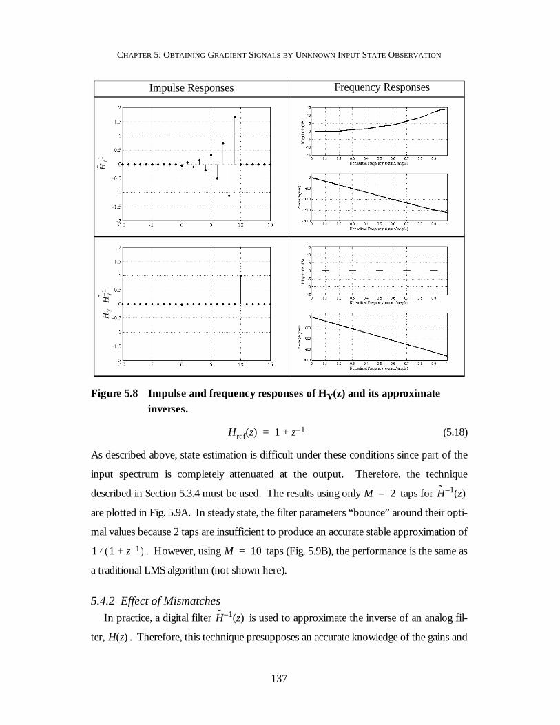
CHAPTER 5: OBTAINING GRADIENT SIGNALS BY UNKNOWN INPUT STATE OBSERVATION
137
(5.18)
As described above, state estimation is difficult under these conditions since part of the
input spectrum is completely attenuated at the output. Therefore, the technique
described in Section 5.3.4 must be used. The results using only taps for
are plotted in Fig. 5.9A. In steady state, the filter parameters “bounce” around their opti-
mal values because 2 taps are insufficient to produce an accurate stable approximation of
. However, using taps (Fig. 5.9B), the performance is the same as
a traditional LMS algorithm (not shown here).
5.4.2 Effect of MismatchesIn practice, a digital filter is used to approximate the inverse of an analog fil-
ter, . Therefore, this technique presupposes an accurate knowledge of the gains and
Figure 5.8 Impulse and frequency responses of HY(z) and its approximate inverses.
HY1–
HY
HY1–
⋅
Impulse Responses Frequency Responses
Href z( ) 1 z 1–+=
M 2= H 1– z( )
1 1 z 1–+( )⁄ M 10=
H 1– z( )
H z( )
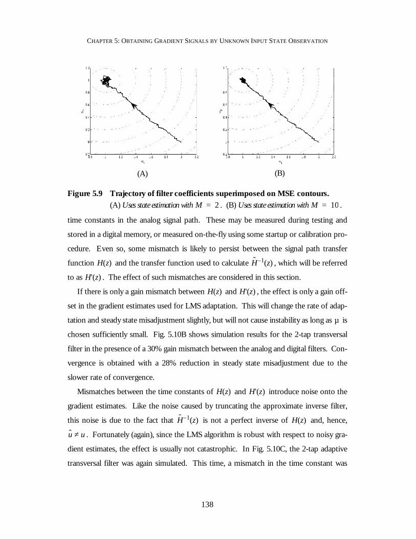
CHAPTER 5: OBTAINING GRADIENT SIGNALS BY UNKNOWN INPUT STATE OBSERVATION
138
time constants in the analog signal path. These may be measured during testing and
stored in a digital memory, or measured on-the-fly using some startup or calibration pro-
cedure. Even so, some mismatch is likely to persist between the signal path transfer
function and the transfer function used to calculate , which will be referred
to as . The effect of such mismatches are considered in this section.
If there is only a gain mismatch between and , the effect is only a gain off-
set in the gradient estimates used for LMS adaptation. This will change the rate of adap-
tation and steady state misadjustment slightly, but will not cause instability as long as is
chosen sufficiently small. Fig. 5.10B shows simulation results for the 2-tap transversal
filter in the presence of a 30% gain mismatch between the analog and digital filters. Con-
vergence is obtained with a 28% reduction in steady state misadjustment due to the
slower rate of convergence.
Mismatches between the time constants of and introduce noise onto the
gradient estimates. Like the noise caused by truncating the approximate inverse filter,
this noise is due to the fact that is not a perfect inverse of and, hence,
. Fortunately (again), since the LMS algorithm is robust with respect to noisy gra-
dient estimates, the effect is usually not catastrophic. In Fig. 5.10C, the 2-tap adaptive
transversal filter was again simulated. This time, a mismatch in the time constant was
Figure 5.9 Trajectory of filter coefficients superimposed on MSE contours.(A) Uses state estimation with . (B) Uses state estimation with .
(A) (B)
M 2= M 10=
H z( ) H 1– z( )
H' z( )
H z( ) H' z( )
µ
H z( ) H' z( )
H 1– z( ) H z( )
u u≠

CHAPTER 5: OBTAINING GRADIENT SIGNALS BY UNKNOWN INPUT STATE OBSERVATION
139
emulated by assuming a 10% mismatch in parameter only (no mismatch in ). This
translates into a 10% discrepancy between the zero frequency of and . The
discrepancy caused no observable difference in convergence rate or misadjustment.
5.4.3 Dc Offset EffectsIn Fig. 5.11A the trajectory of a traditional LMS algorithm is plotted for a 2-tap adap-
tive transversal filter with dc offsets introduced on the state signals, the error signal, and
at the output of the LMS multipliers, as would be expected in an analog circuit imple-
mentation. The dc offsets have magnitudes equal to 0.1% of the RMS input signal
power. The algorithm does not converge to the optimal coefficients in steady state.
However, using the state estimation techniques described here in combination with the
adaptive dc cancellation tap described in the Section 1.3.2, dc offsets have no effect. Fig.
5.11B shows the simulation results using the same dc offsets as before, but this time
using state estimation and an adaptive dc tap. There is no steady state error. As men-
tioned in Chapter 4, the same advantages are obtainable using any digital gradient descent
algorithm in combination with an adaptive dc tap.
5.4.4 5th Order Continuous Time FilterAs a more practical example, the adaptation of a 5th order orthonormal ladder contin-
uous time filter, , was considered. If the continuous time output is sampled at the
Nyquist rate, the combination of the filter and subsequent sampling block can be mod-
Figure 5.10 Two-tap adaptive transversal filter parameter evolution in the presence of mismatches.(A) No mismatch (B) 30% gain mismatch (C) 10% mismatch in the time constant
(A) (B) (C)
Para
met
er V
alue
s
Iterations Iterations Iterations
α1 α2
H z( ) H' z( )
H s( )

CHAPTER 5: OBTAINING GRADIENT SIGNALS BY UNKNOWN INPUT STATE OBSERVATION
140
eled by a discrete time transfer function obtained from via an impulse invari-
ance transformation [7]. State estimation and filter adaptation can then proceed just as
before. Fortunately, in most digital communications applications the output of a contin-
uous time filter is sampled at the Nyquist rate anyway in order to perform clock recovery
and demodulation. Therefore, no additional analog hardware is required for adaptation.
The reference filter for the continuous time simulations was a 5th order elliptic filter,
so had zeros on the -axis. As a result, in steady state, portions of the input
spectrum were completely attenuated at the filter output. However, as long as enough
taps are used in the approximate inverse, the state estimates are still accurate enough to
allow for convergence using the LMS algorithm (Fig. 5.12). Notice that as increases,
the performance approaches that of the standard LMS algorithm. Using simulations like
this one, a value for can be selected based on the amount of excess MSE which can
be tolerated.
5.5 Hardware Requirements
Implementation of an adaptation algorithm using unknown input state observation
requires more complex signal processing than straight LMS adaptation. However, in
Figure 5.11 Trajectory of filter coefficients superimposed on MSE contours. Dc offsets are introduced on all state and error signals.(A) Uses the standard LMS algorithm. (B) Uses state estimation with .
(A) (B)
M 10=
H z( ) H s( )
Href s( ) jω
M
M

CHAPTER 5: OBTAINING GRADIENT SIGNALS BY UNKNOWN INPUT STATE OBSERVATION
141
many digital communications applications a DSP core is integrated along with the analog
front-end and is mostly idle during startup while adaptation is being performed. The
DSP core could be used to perform the state estimation. Specifically, the following digi-
tal signal processing functions are required:
• A digital filter operating at the Nyquist rate on the adapted filter’s output, , is
required to implement the approximate inverse . An FIR filter was used in all
of the behavioral simulations above. The number of taps depends on the order of the
adapted filter, and the amount of noise in the gradient estimate which can be toler-
ated. For the 2nd order transversal filter, 10 taps were used. For the 5th order con-
tinuous time filter, up to 100 taps were used. It might be possible to reduce the
number of computations required by using a recursive filter structure for .
Furthermore, assuming slower convergence can be tolerated, the filter’s speed
requirement can also be relaxed by using a polyphase implementation. This would
entail storing a burst of samples of the filter output in a memory at the Nyquist rate.
The samples would then be processed at a slower clock rate to obtain the input & gra-
Figure 5.12 LMS adaptation of a 5th order orthonormal ladder filter using unknown input state observation.The length of the approximate inverse filter, , is varied from to 100. Simulation results for the standard LMS algorithm are also plotted for comparison.
LMS
M = 100M = 50
M = 25
M = 20
H 1– z( ) M 20=
y k( )
H 1– z( )
H 1– z( )

CHAPTER 5: OBTAINING GRADIENT SIGNALS BY UNKNOWN INPUT STATE OBSERVATION
142
dient estimates, after which one iteration of the LMS update equation could be per-
formed and the entire process repeated. This is very likely to be the strategy used for
any practical integrated implementation.
• A variable delay line is required for the error signal, . The maximum delay is
equal to the length of the FIR implementation of .
• The “controller” in Fig. 5.5 must calculate the approximate inverse transfer function
from a knowledge of the adapted filter parameters, . If this calculation is
repeated at the Nyquist rate using the step-by-step procedure described in Section 5.3,
it would involve considerable overhead: one Taylor series expansion for each adapted
pole or zero involving several digital multiplications and divisions each. However,
only has to be recalculated when changes. It can be recalculated less fre-
quently if a block LMS update rule is used whereby the gradient estimates are aver-
aged for a while before the filter parameters are updated. Further simplifications
might be possible depending upon the exact filter structure. For instance, a simple
and fast realization of the controller would be to use the parameters as the
address to a lookup table where the approximate inverse transfer functions are stored
for all possible combinations of parameter values. As the number of parameter bits
increases, the lookup table will grow large. Depending upon the particular applica-
tion, the best implementation might be a combination of the block LMS algorithm
with lookup tables followed by more accurate calculations.
Of course, unknown input observation implies a savings in analog hardware complex-
ity since sampling of the filter input and state signals is not required. The trade-off of
analog hardware for digital hardware is desirable in many mixed-signal ICs, particularly in
deep submicron CMOS.
5.6 Conclusions
Techniques for state observation which are studied in the control literature either
require access to both the system inputs and outputs, or require the system under obser-
e k( )
H 1– z( )
H 1– z( ) p k( )
H 1– z( ) H z( )
p k( )
p k( )

CHAPTER 5: OBTAINING GRADIENT SIGNALS BY UNKNOWN INPUT STATE OBSERVATION
143
vation to be minimum phase. An approximate time delayed state estimator was pro-
posed which can be applied to any state space system with unknown inputs. This
technique is particularly relevant in analog filters with digitally programmable parameters
since the LMS algorithm requires estimates of the filter’s internal state signals, but it is
impractical to build the additional analog circuitry to generate and digitize them. Instead,
time delayed state estimates are calculated digitally from the filter output and used for
LMS adaptation with minimal additional analog hardware.
The technique is also potentially immune to dc offset effects which usually hinder
analog implementations of the LMS algorithm. Since the state estimates are generated
digitally from the filter output, an adaptive dc tap at the filter output results in state esti-
mates which are offset-free. However, the adaptation algorithm is computationally com-
plex compared to straight LMS adaptation and efficient hardware implementations are
still an open issue.
The general state observation technique is potentially applicable to any adaptation
algorithm where the filter’s state information is required but inaccessible. Although only
the LMS algorithm was discussed here due to its popularity and straightforward imple-
mentation, the state estimates could also be used in (for example) the Newton-Raphson
algorithm.
Filter adaptation using unknown input state observation was verified in behavioral
simulations on a 2-tap adaptive transversal filter and a 5th order continuous time filter.
The approximate inverse filter must have a long enough impulse response to provide
good state estimates, even when the signal path filter has spectral nulls. If the filter
is made long enough, the performance of the adaptation algorithm approaches
that of the standard LMS algorithm.
5.7 References
[1] D.A. Johns, W.M. Snelgrove and A.S. Sedra, “Continuous-Time LMS Adaptive Recursive Filters,” IEEE Trans. Circuits Syst., vol. CAS-38, pp. 769-778, July 1991.
H 1– z( )
CHAPTER 5: OBTAINING GRADIENT SIGNALS BY UNKNOWN INPUT STATE OBSERVATION
144
[2] A. Carusone and D. A. Johns, "Obtaining Digital Gradient Signals for Analog Adaptive Filters," IEEE Int. Symp. Circuits and Syst., May 1999.
[3] R.E. Kalman, “A New Approach to Linear Filtering and Prediction Problems,” ASME J. of Basic Eng., vol. 820, pp. 35-45, 1960.
[4] R.E. Kalman and R.S. Bucy, “New Results in Linear Filtering and Prediction Problems,” ASME J. of Basic Eng., vol. 830, pp. 95-108, 1961.
[5] D.G. Luenberger, “Observing the State of a Linear System,” IEEE Trans. on Military Electronics, vol. MIL-8, pp. 74-80, 1964.
[6] J. Jin, M. Tahk and C. Park, “Time-delayed state and unknown input observation,” Int. J. Control, vol. 66, pp. 733-745, 1997.
[7] A. V. Oppenheim and R. W. Schafer, Digital Signal Processing, Prentice-Hall, Englewood Cliffs, N.J., 1975.

145
Chapter 6
Conclusion
6.1 Summary
The problems that limit the use of analog adaptive filters in modern integrated sys-
tems were studied. Chief among those problems are analog circuit complexity (particu-
larly in deep submicron CMOS process technologies) and dc offset effects. The
problems are overcome by combining a digitally programmable analog filter in the signal
path with a digital adaptation algorithm. Both the analog circuits and the digital adapta-
tion algorithms were discussed.
Chapter 2 described several circuit techniques for implementing a digitally program-
mable analog filter in a CMOS process technology. The techniques were verified in hard-
ware on a prototype 5th order integrated filter with all poles and zeros digitally
programmable. Although the results were modest (particularly the linearity), the degree
of programmability realized had previously only been reported in BiCMOS processes
with cutoff frequencies below 10 MHz [1] (compared with up to 70 MHz in this work).
The remainder of the thesis sought to alleviate the LMS algorithm’s need for direct
access to the filter’s internal state signals by performing some additional signal processing
digitally. Three techniques were described: Chapter 3, the dithered linear search (DLS);
Chapter 4, the LMS algorithm with a co-ordinate transform (LMS-CT and LMS-ICT);
and Chapter 5, the LMS algorithm using an unknown input state observer (LMS with
UIO). All three are compared qualitatively in terms of their performance and complexity

CHAPTER 6: CONCLUSION
146
in Table 6.1. All compare favorably with the LMS algorithm in terms of analog circuit
complexity. This is the most important criteria in many data communication systems
since the performance requirements are not stringent and digital circuits are relatively
easy and cheap to integrate in deep submicron CMOS. The DLS algorithm is simple and
general, but its rate of convergence is orders of magnitude slower than the others restrict-
ing it to applications where slow adaptation can be tolerated. The LMS algorithm with a
UIO converges quickly (at the same rate as the LMS algorithm) but has the greatest com-
putational complexity (and, as a result, was not verified on the prototype filter). The
LMS-CT/ICT algorithms combine a simple hardware implementation with performance
identical to the LMS algorithm making them preferable to the LMS algorithm for almost
any analog adaptive linear combiner in a mixed signal application. Unfortunately, the
LMS-CT/ICT algorithms can not be used to adapt filter poles.
6.2 Future Work
The digital adaptation algorithms in this thesis have been presented without reference
to any particular application in order to highlight their generality. The logical next step is
to target a specific application in order to demonstrate their practicality. Applications
where analog adaptive filters offer practical advantages over digital adaptive filters are
generally restricted to those where all of the following criteria apply:
Algorithm LMS DLS LMS-CT/ICT LMS with UIO
Adaptation rate Fast Slow Fast Fast
Analog circuit complexity High Low Low Low
Digital circuit complexity Lowa
a. Digital circuit complexity is significantly reduced by using signed variations.
Low Mediuma High
Applicable filter structures
Any with a uni-modal perfor-mance surface
Any with a uni-modal perfor-mance surface
Adaptive Linear Combiner
Any with a uni-modal perfor-mance surface
Table 6.1 Comparison of digital algorithms for analog adaptive filters.

CHAPTER 6: CONCLUSION
147
1. The input signal already exists in analog form, so that additional data converters are
not required to perform the filtering in the analog domain.
2. Only moderate linearity is required, because high linearity (> 50 dB) is difficult to
achieve in analog circuitry with low supply voltages.
3. High speed and/or low power are important design objectives, otherwise digital cir-
cuits are efficient and easier to implement.
All of the applications discussed in Section 1.2 meet these criteria, with the possible
exception of magnetic storage read channels where CMOS process scaling appears to
have allowed digital adaptive filters to catch up to the system requirements [2] and analog
adaptive filters are losing favor. The most promising candidates in the near-term are
long haul fibre optic and short-distance very-high-speed wired (including chip-to-chip)
channels. In these applications, filter zeros could be adapted quickly and with low com-
plexity using a subsampled SS-LMS-ICT algorithm providing programmable high-fre-
quency boost to equalize the lowpass channels. Furthermore, the linearity requirements
are modest since very few data levels are transmitted, and a digital approach is unlikely to
be practical at the targeted speeds (10+ Gb/s) in the near future.
Several other potential topics for future study suggest themselves:
• Integrated implementation: An obvious extension would be to prototype an ana-
log adaptive filter integrated alongside one of the digital adaptation algorithms
described above. This would be particularly interesting for the LMS algorithm with a
UIO since it is not clear how to efficiently implement the required digital signal pro-
cessing in hardware.
• Programmable analog signal conditioner: The circuit techniques that were proven
successful in Chapter 2 could be used to implement a highly programmable analog
Gm-C filter in 0.18 µm CMOS. Based upon the experience gained from the proto-
type filter design, realistic design specifications would be a filter with 40 dB linearity
and poles & zeros that are digitally programmable beyond 100 MHz. Such a block
could be used as a general analog signal conditioner in a wide range of applications,
and would be far beyond any previously reported digitally configurable analog filter.

CHAPTER 6: CONCLUSION
148
• Further stability analyses: General stability proofs of the adaptation algorithms
described in this thesis are still lacking. Stability of the DLS algorithm using multilevel
dither was not verified analytically. Neither was stability of the signed variations of the
LMS-CT and LMS-ICT algorithms. The LMS algorithm with a UIO uses heuristic
techniques to perform gradient estimation when there is a transmission zero in the
adapted filter; further stability analysis is also warranted here.
• Exploration of other dither signals: Other, possibly multilevel, dither signals may
offer advantages over either pseudorandom or Hadamard sequence dither. One pos-
sibility is to use delta-sigma modulation to shift the dither energy outside of the
adapted filter’s bandwidth of interest.
• Use of UIO for other applications: Although the technique developed for
unknown input state observation in Chapter 5 was intended for gradient estimation in
analog filter adaptation, the same technique could be useful anywhere an approximate,
time delayed, unknown input state observer is needed. It would be interesting to
explore other applications for the technique.
• Combine algorithms: It might be possible to combine the different algorithms in
the adaptation of a single filter to take advantage of the merits of each. For instance,
the DLS could be used during startup to adapt the filter’s poles. Then, the LMS-ICT
could be used to adapt the zeros. The input sampling circuit required by the LMS-
ICT could be eliminated by using the approximate inverse technique from Chapter 5
to obtain estimates of the filter input from its output.
6.3 References
[1] A. Hematy and G. W. Roberts, “A Fully-Programmable Analog Log-Domain Filter Circuit,” 1998 IEEE Int. Conf. Circuits and Syst., pp. 309-312, May 1998.
[2] S. Rylov, A. Rylyakov, J. Tierno, M. Immediato, M. Beakes, M. Kapur, P. Ampadu, and D. Pearson, “A 2.3 GSample/s 10-tap Digital FIR Filter for Magnetic Recording Read Channels,” IEEE Int. Solid-State Circuits Conf. Dig. Tech. Papers, pp. 190-191, Feb. 2001.


